JP4772228B2 - Method for manufacturing light emitting device - Google Patents
Method for manufacturing light emitting device Download PDFInfo
- Publication number
- JP4772228B2 JP4772228B2 JP2001223863A JP2001223863A JP4772228B2 JP 4772228 B2 JP4772228 B2 JP 4772228B2 JP 2001223863 A JP2001223863 A JP 2001223863A JP 2001223863 A JP2001223863 A JP 2001223863A JP 4772228 B2 JP4772228 B2 JP 4772228B2
- Authority
- JP
- Japan
- Prior art keywords
- conductive layer
- tft
- layer
- insulating film
- semiconductor layer
- Prior art date
- Legal status (The legal status is an assumption and is not a legal conclusion. Google has not performed a legal analysis and makes no representation as to the accuracy of the status listed.)
- Expired - Fee Related
Links
- 238000000034 method Methods 0.000 title claims description 70
- 238000004519 manufacturing process Methods 0.000 title claims description 19
- 239000012535 impurity Substances 0.000 claims description 105
- 238000005530 etching Methods 0.000 claims description 55
- 239000004065 semiconductor Substances 0.000 claims description 55
- 239000000758 substrate Substances 0.000 claims description 28
- 239000010408 film Substances 0.000 description 159
- 239000010410 layer Substances 0.000 description 147
- 239000000463 material Substances 0.000 description 32
- 230000008569 process Effects 0.000 description 24
- XUIMIQQOPSSXEZ-UHFFFAOYSA-N Silicon Chemical compound [Si] XUIMIQQOPSSXEZ-UHFFFAOYSA-N 0.000 description 22
- 229910052710 silicon Inorganic materials 0.000 description 22
- 239000010703 silicon Substances 0.000 description 22
- 239000011229 interlayer Substances 0.000 description 19
- MZLGASXMSKOWSE-UHFFFAOYSA-N tantalum nitride Chemical compound [Ta]#N MZLGASXMSKOWSE-UHFFFAOYSA-N 0.000 description 14
- 230000015572 biosynthetic process Effects 0.000 description 12
- 238000010586 diagram Methods 0.000 description 12
- 239000007789 gas Substances 0.000 description 12
- 238000002347 injection Methods 0.000 description 12
- 239000007924 injection Substances 0.000 description 12
- 239000003990 capacitor Substances 0.000 description 11
- OAICVXFJPJFONN-UHFFFAOYSA-N Phosphorus Chemical compound [P] OAICVXFJPJFONN-UHFFFAOYSA-N 0.000 description 10
- 230000006866 deterioration Effects 0.000 description 10
- PCHJSUWPFVWCPO-UHFFFAOYSA-N gold Chemical group [Au] PCHJSUWPFVWCPO-UHFFFAOYSA-N 0.000 description 10
- 229910052698 phosphorus Inorganic materials 0.000 description 10
- 239000011574 phosphorus Substances 0.000 description 10
- 229910052760 oxygen Inorganic materials 0.000 description 9
- 238000005268 plasma chemical vapour deposition Methods 0.000 description 9
- PXHVJJICTQNCMI-UHFFFAOYSA-N Nickel Chemical compound [Ni] PXHVJJICTQNCMI-UHFFFAOYSA-N 0.000 description 8
- 238000002425 crystallisation Methods 0.000 description 7
- 229910052739 hydrogen Inorganic materials 0.000 description 7
- 238000002161 passivation Methods 0.000 description 7
- 239000000565 sealant Substances 0.000 description 7
- VYPSYNLAJGMNEJ-UHFFFAOYSA-N silicon dioxide Inorganic materials O=[Si]=O VYPSYNLAJGMNEJ-UHFFFAOYSA-N 0.000 description 7
- ZOXJGFHDIHLPTG-UHFFFAOYSA-N Boron Chemical compound [B] ZOXJGFHDIHLPTG-UHFFFAOYSA-N 0.000 description 6
- 229910052581 Si3N4 Inorganic materials 0.000 description 6
- 238000001994 activation Methods 0.000 description 6
- QVGXLLKOCUKJST-UHFFFAOYSA-N atomic oxygen Chemical compound [O] QVGXLLKOCUKJST-UHFFFAOYSA-N 0.000 description 6
- 229910052796 boron Inorganic materials 0.000 description 6
- 230000005525 hole transport Effects 0.000 description 6
- 239000011159 matrix material Substances 0.000 description 6
- 239000001301 oxygen Substances 0.000 description 6
- 230000001681 protective effect Effects 0.000 description 6
- 239000011347 resin Substances 0.000 description 6
- 229920005989 resin Polymers 0.000 description 6
- HQVNEWCFYHHQES-UHFFFAOYSA-N silicon nitride Chemical compound N12[Si]34N5[Si]62N3[Si]51N64 HQVNEWCFYHHQES-UHFFFAOYSA-N 0.000 description 6
- 229910052814 silicon oxide Inorganic materials 0.000 description 6
- 238000004544 sputter deposition Methods 0.000 description 6
- 238000000137 annealing Methods 0.000 description 5
- 230000008025 crystallization Effects 0.000 description 5
- 230000000694 effects Effects 0.000 description 5
- 238000009616 inductively coupled plasma Methods 0.000 description 5
- 238000000059 patterning Methods 0.000 description 5
- 238000007789 sealing Methods 0.000 description 5
- UFHFLCQGNIYNRP-UHFFFAOYSA-N Hydrogen Chemical compound [H][H] UFHFLCQGNIYNRP-UHFFFAOYSA-N 0.000 description 4
- 239000000956 alloy Substances 0.000 description 4
- 229910021417 amorphous silicon Inorganic materials 0.000 description 4
- 239000012298 atmosphere Substances 0.000 description 4
- UMIVXZPTRXBADB-UHFFFAOYSA-N benzocyclobutene Chemical compound C1=CC=C2CCC2=C1 UMIVXZPTRXBADB-UHFFFAOYSA-N 0.000 description 4
- 239000000969 carrier Substances 0.000 description 4
- 239000003795 chemical substances by application Substances 0.000 description 4
- 239000011521 glass Substances 0.000 description 4
- 238000010438 heat treatment Methods 0.000 description 4
- 239000001257 hydrogen Substances 0.000 description 4
- 150000002500 ions Chemical class 0.000 description 4
- 229910052759 nickel Inorganic materials 0.000 description 4
- 229910052757 nitrogen Inorganic materials 0.000 description 4
- -1 polyphenylene vinylene Polymers 0.000 description 4
- XLOMVQKBTHCTTD-UHFFFAOYSA-N Zinc monoxide Chemical compound [Zn]=O XLOMVQKBTHCTTD-UHFFFAOYSA-N 0.000 description 3
- 230000001133 acceleration Effects 0.000 description 3
- NIXOWILDQLNWCW-UHFFFAOYSA-N acrylic acid group Chemical group C(C=C)(=O)O NIXOWILDQLNWCW-UHFFFAOYSA-N 0.000 description 3
- 230000004913 activation Effects 0.000 description 3
- 229910045601 alloy Inorganic materials 0.000 description 3
- 229910052782 aluminium Inorganic materials 0.000 description 3
- 150000001875 compounds Chemical class 0.000 description 3
- 238000005984 hydrogenation reaction Methods 0.000 description 3
- 229910003437 indium oxide Inorganic materials 0.000 description 3
- PJXISJQVUVHSOJ-UHFFFAOYSA-N indium(iii) oxide Chemical compound [O-2].[O-2].[O-2].[In+3].[In+3] PJXISJQVUVHSOJ-UHFFFAOYSA-N 0.000 description 3
- 239000011810 insulating material Substances 0.000 description 3
- 239000004973 liquid crystal related substance Substances 0.000 description 3
- 239000000203 mixture Substances 0.000 description 3
- 230000010355 oscillation Effects 0.000 description 3
- 230000003647 oxidation Effects 0.000 description 3
- 238000007254 oxidation reaction Methods 0.000 description 3
- 238000000206 photolithography Methods 0.000 description 3
- 229920003227 poly(N-vinyl carbazole) Polymers 0.000 description 3
- 229920000553 poly(phenylenevinylene) Polymers 0.000 description 3
- 239000002861 polymer material Substances 0.000 description 3
- 230000009467 reduction Effects 0.000 description 3
- 239000002356 single layer Substances 0.000 description 3
- 239000000126 substance Substances 0.000 description 3
- 229910052715 tantalum Inorganic materials 0.000 description 3
- 238000001039 wet etching Methods 0.000 description 3
- IJGRMHOSHXDMSA-UHFFFAOYSA-N Atomic nitrogen Chemical compound N#N IJGRMHOSHXDMSA-UHFFFAOYSA-N 0.000 description 2
- 239000004952 Polyamide Substances 0.000 description 2
- 239000004642 Polyimide Substances 0.000 description 2
- BOTDANWDWHJENH-UHFFFAOYSA-N Tetraethyl orthosilicate Chemical compound CCO[Si](OCC)(OCC)OCC BOTDANWDWHJENH-UHFFFAOYSA-N 0.000 description 2
- XAGFODPZIPBFFR-UHFFFAOYSA-N aluminium Chemical compound [Al] XAGFODPZIPBFFR-UHFFFAOYSA-N 0.000 description 2
- 230000008901 benefit Effects 0.000 description 2
- 239000003054 catalyst Substances 0.000 description 2
- 238000006243 chemical reaction Methods 0.000 description 2
- 229910052802 copper Inorganic materials 0.000 description 2
- 229910021419 crystalline silicon Inorganic materials 0.000 description 2
- 238000001312 dry etching Methods 0.000 description 2
- 238000001704 evaporation Methods 0.000 description 2
- 239000011152 fibreglass Substances 0.000 description 2
- 230000005669 field effect Effects 0.000 description 2
- 229910010272 inorganic material Inorganic materials 0.000 description 2
- 239000011147 inorganic material Substances 0.000 description 2
- 238000005224 laser annealing Methods 0.000 description 2
- 238000005499 laser crystallization Methods 0.000 description 2
- 239000012299 nitrogen atmosphere Substances 0.000 description 2
- 230000003287 optical effect Effects 0.000 description 2
- 238000001020 plasma etching Methods 0.000 description 2
- 239000004033 plastic Substances 0.000 description 2
- 229920003023 plastic Polymers 0.000 description 2
- 229920002647 polyamide Polymers 0.000 description 2
- 229910021420 polycrystalline silicon Inorganic materials 0.000 description 2
- 229920001721 polyimide Polymers 0.000 description 2
- 229920002620 polyvinyl fluoride Polymers 0.000 description 2
- 230000004044 response Effects 0.000 description 2
- 238000003860 storage Methods 0.000 description 2
- 239000010936 titanium Substances 0.000 description 2
- 229910052721 tungsten Inorganic materials 0.000 description 2
- 238000007740 vapor deposition Methods 0.000 description 2
- 150000005072 1,3,4-oxadiazoles Chemical class 0.000 description 1
- 239000004925 Acrylic resin Substances 0.000 description 1
- 229920000178 Acrylic resin Polymers 0.000 description 1
- 229920002799 BoPET Polymers 0.000 description 1
- 239000005041 Mylar™ Substances 0.000 description 1
- 229910052779 Neodymium Inorganic materials 0.000 description 1
- 229910000577 Silicon-germanium Inorganic materials 0.000 description 1
- 229910001069 Ti alloy Inorganic materials 0.000 description 1
- NRTOMJZYCJJWKI-UHFFFAOYSA-N Titanium nitride Chemical compound [Ti]#N NRTOMJZYCJJWKI-UHFFFAOYSA-N 0.000 description 1
- LEVVHYCKPQWKOP-UHFFFAOYSA-N [Si].[Ge] Chemical compound [Si].[Ge] LEVVHYCKPQWKOP-UHFFFAOYSA-N 0.000 description 1
- 230000003213 activating effect Effects 0.000 description 1
- 239000005407 aluminoborosilicate glass Substances 0.000 description 1
- 229910052785 arsenic Inorganic materials 0.000 description 1
- RQNWIZPPADIBDY-UHFFFAOYSA-N arsenic atom Chemical compound [As] RQNWIZPPADIBDY-UHFFFAOYSA-N 0.000 description 1
- 229910052788 barium Inorganic materials 0.000 description 1
- DSAJWYNOEDNPEQ-UHFFFAOYSA-N barium atom Chemical compound [Ba] DSAJWYNOEDNPEQ-UHFFFAOYSA-N 0.000 description 1
- 230000000903 blocking effect Effects 0.000 description 1
- 239000005388 borosilicate glass Substances 0.000 description 1
- 230000015556 catabolic process Effects 0.000 description 1
- 229910052804 chromium Inorganic materials 0.000 description 1
- 238000004891 communication Methods 0.000 description 1
- 229920000547 conjugated polymer Polymers 0.000 description 1
- VBVAVBCYMYWNOU-UHFFFAOYSA-N coumarin 6 Chemical compound C1=CC=C2SC(C3=CC4=CC=C(C=C4OC3=O)N(CC)CC)=NC2=C1 VBVAVBCYMYWNOU-UHFFFAOYSA-N 0.000 description 1
- 239000013078 crystal Substances 0.000 description 1
- 230000007547 defect Effects 0.000 description 1
- 238000007872 degassing Methods 0.000 description 1
- 238000011161 development Methods 0.000 description 1
- ZOCHARZZJNPSEU-UHFFFAOYSA-N diboron Chemical compound B#B ZOCHARZZJNPSEU-UHFFFAOYSA-N 0.000 description 1
- 238000007599 discharging Methods 0.000 description 1
- 230000005684 electric field Effects 0.000 description 1
- 238000005516 engineering process Methods 0.000 description 1
- 239000003822 epoxy resin Substances 0.000 description 1
- 125000005678 ethenylene group Chemical group [H]C([*:1])=C([H])[*:2] 0.000 description 1
- 239000007850 fluorescent dye Substances 0.000 description 1
- AMGQUBHHOARCQH-UHFFFAOYSA-N indium;oxotin Chemical compound [In].[Sn]=O AMGQUBHHOARCQH-UHFFFAOYSA-N 0.000 description 1
- 239000011261 inert gas Substances 0.000 description 1
- 238000005468 ion implantation Methods 0.000 description 1
- 238000004518 low pressure chemical vapour deposition Methods 0.000 description 1
- 230000014759 maintenance of location Effects 0.000 description 1
- 229910052751 metal Inorganic materials 0.000 description 1
- 239000002184 metal Substances 0.000 description 1
- 229910052750 molybdenum Inorganic materials 0.000 description 1
- QJGQUHMNIGDVPM-UHFFFAOYSA-N nitrogen group Chemical group [N] QJGQUHMNIGDVPM-UHFFFAOYSA-N 0.000 description 1
- 229910052763 palladium Inorganic materials 0.000 description 1
- 229920000647 polyepoxide Polymers 0.000 description 1
- 229920000728 polyester Polymers 0.000 description 1
- 229920002098 polyfluorene Polymers 0.000 description 1
- 229920000642 polymer Polymers 0.000 description 1
- 229920005591 polysilicon Polymers 0.000 description 1
- 238000012545 processing Methods 0.000 description 1
- 239000010453 quartz Substances 0.000 description 1
- 238000004151 rapid thermal annealing Methods 0.000 description 1
- 239000012495 reaction gas Substances 0.000 description 1
- 230000006798 recombination Effects 0.000 description 1
- 238000005215 recombination Methods 0.000 description 1
- 238000011160 research Methods 0.000 description 1
- 238000012827 research and development Methods 0.000 description 1
- SBEQWOXEGHQIMW-UHFFFAOYSA-N silicon Chemical group [Si].[Si] SBEQWOXEGHQIMW-UHFFFAOYSA-N 0.000 description 1
- HBMJWWWQQXIZIP-UHFFFAOYSA-N silicon carbide Chemical compound [Si+]#[C-] HBMJWWWQQXIZIP-UHFFFAOYSA-N 0.000 description 1
- 229910010271 silicon carbide Inorganic materials 0.000 description 1
- 229910052709 silver Inorganic materials 0.000 description 1
- 238000009751 slip forming Methods 0.000 description 1
- 239000000243 solution Substances 0.000 description 1
- 125000006850 spacer group Chemical group 0.000 description 1
- GUVRBAGPIYLISA-UHFFFAOYSA-N tantalum atom Chemical compound [Ta] GUVRBAGPIYLISA-UHFFFAOYSA-N 0.000 description 1
- 238000002230 thermal chemical vapour deposition Methods 0.000 description 1
- 239000010409 thin film Substances 0.000 description 1
- XOLBLPGZBRYERU-UHFFFAOYSA-N tin dioxide Chemical compound O=[Sn]=O XOLBLPGZBRYERU-UHFFFAOYSA-N 0.000 description 1
- 229910001887 tin oxide Inorganic materials 0.000 description 1
- 229910052719 titanium Inorganic materials 0.000 description 1
- NXHILIPIEUBEPD-UHFFFAOYSA-H tungsten hexafluoride Chemical compound F[W](F)(F)(F)(F)F NXHILIPIEUBEPD-UHFFFAOYSA-H 0.000 description 1
- 239000011787 zinc oxide Substances 0.000 description 1
Images


Landscapes
- Electroluminescent Light Sources (AREA)
- Devices For Indicating Variable Information By Combining Individual Elements (AREA)
- Thin Film Transistor (AREA)
Description
【0001】
【発明の属する技術分野】
本発明は、薄膜トランジスタ(以下TFTという)で構成された回路を有する発光装置及びその作製方法に関する。なお、本明細書中における発光装置とは、電界を加えることで発光が得られる発光素子を有する画像表示デバイス等のデバイスを指す。また、発光素子にコネクター、例えば異方導電性フィルム((FPC:flexible printed circuit)もしくはTAB(Tape Automated Bonding)テープもしくはTCP(Tape Carrier Package)が取り付けられたモジュール、TABテープやTCPの先にプリント配線板が設けられたモジュール、または発光素子にCOG(Chip On Glass)方式によりIC(集積回路)が直接実装されたモジュールも全て発光装置に含む他、発光装置を部品として搭載した電気器具も範疇に含んでいる。
【0002】
【従来の技術】
近年、基板上にTFTを形成する技術が大幅に進歩し、アクティブマトリクス型表示装置への応用開発が進められている。特に、ポリシリコン膜を用いたTFTは、従来のアモルファスシリコン膜を用いたTFTよりも電界効果移動度(モビリティともいう)が高いので、高速動作が可能である。そのため、従来、基板外の駆動回路で行っていた画素の制御を、画素と同一の基板上に形成した駆動回路で行うことが可能となっている。
【0003】
このようなアクティブマトリクス型の表示装置は、同一基板上に様々な回路や素子を作り込むことで製造コストの低減、電気光学装置の小型化、歩留まりの上昇、スループットの低減など、様々な利点が得られる。
【0004】
また、自発光型の素子としてEL素子を有したアクティブマトリクス型の発光装置の研究が活発化している。
【0005】
なお、本明細書におけるEL素子は一対の電極(陽極と陰極)間にEL層が挟まれた構造となっているが、EL層は通常、積層構造となっている。代表的には、コダック・イーストマン・カンパニーのTangらが提案した「正孔輸送層/発光層/電子輸送層」という積層構造が挙げられる。この構造は非常に発光効率が高く、現在、研究開発が進められている発光装置は殆どこの構造を採用している。
【0006】
また他にも、陽極上に正孔注入層/正孔輸送層/発光層/電子輸送層、または正孔注入層/正孔輸送層/発光層/電子輸送層/電子注入層の順に積層する構造でも良い。発光層に対して蛍光性色素等をドーピングすることも可能である。
【0007】
本明細書において陰極と陽極の間に設けられる全ての層を総称してEL層と呼ぶ。よって上述した正孔注入層、正孔輸送層、発光層、電子輸送層、電子注入層等は、全てEL層に含まれる。
【0008】
そして、上記構造でなるEL層に一対の電極から所定の電圧をかけ、それにより発光層においてキャリアの再結合が起こって発光する。なお、ここで得られる発光には、蛍光及び燐光が含まれる。また、本明細書中では、陽極、EL層及び陰極で形成される発光素子をEL素子と呼ぶ。
【0009】
EL素子が有するEL層は熱、光、水分、酸素等によって劣化が促進されることから、一般的にアクティブマトリクス型の発光装置の作製において、画素部に配線やTFTを形成した後にEL素子が形成される。
【0010】
アクティブマトリクス型の発光装置は、各画素のそれぞれにTFTでなるスイッチング素子を設けそのスイッチング素子(スイッチング用TFT)によって電流制御を行う駆動素子(電流制御用TFT)を動作させてEL層(発光層)を発光させる。例えば特開平10−189252号に記載された発光装置がある。
【0011】
なお、画素部におけるスイッチング用TFTおよび電流制御用TFT
は、低いオフ電流(Ioff)が要求されている。オフ電流を低減するためのTFT構造として、ゲート電極がゲート絶縁膜を介して低濃度不純物領域と重ならない領域(LDD領域)を有する構造が知られている。
【0012】
これに対して、画像表示を行う画像回路や画像回路を制御するための駆動回路は、高い駆動能力(オン電流:Ion)およびホットキャリア効果による劣化を防ぎ信頼性を向上させることが求められている。ホットキャリアによるオン電流値の劣化を防ぐのに有効である構造としては、ゲート電極がゲート絶縁膜を介して低濃度不純物領域と重なる領域(GOLD領域)を有する構造が知られている。
【0013】
【発明が解決しようとする課題】
しかし、LDD領域を有するTFTやGOLD領域を有するTFTを形成しようとすると、その製造工程は複雑なものになってしまう。本発明では、アクティブマトリクス型の発光装置において、その駆動回路に用いられるTFTは、高い駆動能力(オン電流)と信頼性を有し、一方で、画素部に用いられるTFTは、オフ電流が低くなるようにし、また、この作製行程を少ないマスク数で実現させることを目的とする。
【0014】
【発明を解決するための手段】
本発明では、同一基板上に形成されるTFTのうちで、駆動回路に用いるnチャネル型TFTを導電層からなるゲート電極と重なる位置に低濃度不純物領域(GOLD領域)を有する構造で作製する。一方、画素部に用いるnチャネル型TFTは、ゲート電極と重ならない位置に低濃度不純物領域(LDD領域)を有する構造で作製する。
【0015】
GOLD領域を有するTFTは、TFTにおけるホットキャリアの注入による劣化を防ぐのに適した構造であり、また、オン電流が高いことから駆動回路に適した構造である。
【0016】
また、LDD領域を有するTFTは、オフ電流が低くなる構造であることから、画素部におけるTFTとして適した構造である。
【0017】
さらに、pチャネル型TFTは、nチャネル型TFTの不純物領域に不純物をドーピングすることにより作製する。なお、このときLDD領域を有するnチャネル型TFTを用いてドーピングすると、GOLD領域を有するnチャネル型TFTに不純物をドーピングする際に生じるゲート電極の膜厚による不純物濃度のバラツキを抑えることができる。
【0018】
よって、以上のような構造のTFTを同一基板上に形成することにより、駆動回路及び画素部に適するTFTを備えるような発光装置を作製することができる。
【0019】
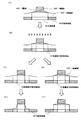
【発明の実施の形態】
本発明の実施の形態について、図1を用いて詳細に説明する。図1(A)において、102はSiからなる半導体層であり、半導体層の一部に導電層からなるゲート電極を形成する。なお、ここでは、TaNからなるゲート電極1(104)、Wからなるゲート電極2(105)の積層構造になっており、このゲート電極をマスクにして、珪素を含む絶縁膜からなるゲート絶縁膜103を介して不純物(リン)をドーピングすることにより、高濃度不純物領域106が形成される。なお、高濃度不純物領域106は、最終的にnチャネル型TFTのソース領域およびドレイン領域となる。
【0020】
そして、再び不純物(リン)をドーピングすることにより、低濃度不純物領域a(107)を形成する。ただし、この低濃度不純物領域a(107)に含まれる不純物の濃度は、先の高濃度不純物領域に含まれるよりも濃度が低くなるように形成する(図1(B))。なお、このような低濃度不純物領域のことをLDD(LDD:Lightly Doped Drain)領域と呼ぶ。なお、ここで形成される低濃度不純物領域a(107)は、ゲート電極とゲート絶縁膜を介して重なっていることからGOLD(Gate-drain Overlapped LDD)領域と呼ばれる。
【0021】
次にエッチング処理を行う。この時ゲート電極1(104)がエッチングされたTFTは、図1(C)に示す構造を有する。具体的には、図1(B)でゲート電極1(104)に重なる位置に形成されていた不純物領域b(107)は、ゲート電極1(104)がエッチングされたことにより、ゲート電極1(104)に重ならない低濃度不純物領域b(108)となる。
【0022】
これに対して、ゲート電極1(104)がエッチングされないようにマスクを形成していた場合には、低濃度不純物領域a(107)を有する図1(D)の構造を形成することができる。
【0023】
そして、ゲート絶縁膜103を全体的にエッチングすると、図1(E)および図1(F)に示すように不純物領域106が露出しており、かつ構造の異なるnチャネル型TFTを同一基板上に形成することができる。
【0024】
なお、図1(C)に示す構造のnチャネル型TFTは、低濃度不純物領域がゲート電極に重ならない領域(LDD領域)を有するため、オフ電流を低くすることができるので画素部に用いる。また、図1(D)に示す構造のnチャネル型TFTは、低濃度不純物領域がゲート電極に重なる構造(GOLD領域)を有するため、オン電流を高めることができ、さらにホットキャリアによる劣化を防ぐことができるので、駆動回路に用いる。
【0025】
さらに図1(E)に示す構造のnチャネル型TFTに不純物(ボロン)をドーピングして、pチャネル型TFTを作製する。このとき、図1(E)の構造を有していればSi上のゲート絶縁膜103を介して不純物(ボロン)をドーピングすることになるため、図1(F)に示す構造のnチャネル型TFTに不純物(ボロン)をドーピングする場合に生じるようなゲート電極1(104)のTaNの膜厚による不純物ドープ量のバラツキを防ぐことができる。つまり、不純物領域における不純物濃度の均一なpチャネル型TFTを作製することができる。
【0026】
なお、ここで作製したpチャネル型TFTは、駆動回路及び画素部に用いている。しかし、駆動回路におけるpチャネル型TFTは、これに限られることはなく図1(F)に示す構造のnチャネル型TFTに不純物(ボロン)をドーピングすることにより作製したpチャネル型TFTを用いても良い。
【0027】
以下に本発明の実施の例を説明する。なお、以下の実施例は好ましい例であり、本発明の発光装置は、以下の実施例に限定されるわけではない。
【0028】
【実施例】
〔実施例1〕
ここでは、本発明を実施して同一基板上に画素部と、画素部の周辺に設ける駆動回路のTFT(nチャネル型TFT及びpチャネル型TFT)を同時に作製する方法について詳細に図2〜図5を用いて説明する。
【0029】
まず、本実施例ではコーニング社の#7059ガラスや#1737ガラスなどに代表されるバリウムホウケイ酸ガラス、またはアルミノホウケイ酸ガラスなどのガラスからなる基板300を用いる。なお、基板300としては、透光性を有する基板であれば限定されず、石英基板を用いても良い。また、本実施例の処理温度に耐えうる耐熱性を有するプラスチック基板を用いてもよい。
【0030】
次いで、基板300上に酸化珪素膜、窒化珪素膜または酸化窒化珪素膜などの絶縁膜から成る下地膜301を形成する。本実施例では下地膜301として2層構造を用いるが、前記絶縁膜の単層膜または2層以上積層させた構造を用いても良い。下地膜301の一層目としては、プラズマCVD法を用い、SiH4、NH3、及びN2Oを反応ガスとして成膜される酸化窒化珪素膜301aを10〜200nm(好ましくは50〜100nm)形成する。本実施例では、膜厚50nmの酸化窒化珪素膜301a(組成比Si=32%、O=27%、N=24%、H=17%)を形成した。次いで、下地膜301のニ層目としては、プラズマCVD法を用い、SiH4、及びN2Oを反応ガスとして成膜される酸化窒化珪素膜301bを50〜200nm(好ましくは100〜150nm)の厚さに積層形成する。本実施例では、膜厚100nmの酸化窒化珪素膜301b(組成比Si=32%、O=59%、N=7%、H=2%)を形成した。
【0031】
次いで、下地膜上に半導体層302〜305を形成する。半導体層302〜305は、非晶質構造を有する半導体膜を公知の手段(スパッタ法、LPCVD法、またはプラズマCVD法等)により成膜した後、公知の結晶化処理(レーザー結晶化法、熱結晶化法、またはニッケルなどの触媒を用いた熱結晶化法等)を行って得られた結晶質半導体膜を所望の形状にパターニングして形成する。この半導体層302〜305の厚さは25〜80nm(好ましくは30〜60nm)の厚さで形成する。結晶質半導体膜の材料に限定はないが、好ましくは珪素(シリコン)またはシリコンゲルマニウム(SiXGe1-X(X=0.0001〜0.02))合金などで形成すると良い。本実施例では、プラズマCVD法を用い、55nmの非晶質珪素膜を成膜した後、ニッケルを含む溶液を非晶質珪素膜上に保持させた。この非晶質珪素膜に脱水素化(500℃、1時間)を行った後、熱結晶化(550℃、4時間)を行い、さらに結晶化を改善するためのレーザーアニ―ル処理を行って結晶質珪素膜を形成した。そして、この結晶質珪素膜をフォトリソグラフィ法を用いたパターニング処理によって、半導体層302〜305を形成した。
【0032】
また、半導体層302〜305を形成した後、TFTのしきい値を制御するために微量な不純物元素(ボロンまたはリン)のドーピングを行ってもよい。
【0033】
また、レーザー結晶化法で結晶質半導体膜を作製する場合には、パルス発振型または連続発光型のエキシマレーザーやYAGレーザー、YVO4レーザーを用いることができる。これらのレーザーを用いる場合には、レーザー発振器から放射されたレーザー光を光学系で線状に集光し半導体膜に照射する方法を用いると良い。結晶化の条件は実施者が適宣選択するものであるが、エキシマレーザーを用いる場合はパルス発振周波数300Hzとし、レーザーエネルギー密度を100〜400mJ/cm2(代表的には200〜300mJ/cm2)とする。また、YAGレーザーを用いる場合にはその第2高調波を用いパルス発振周波数30〜300Hzとし、レーザーエネルギー密度を300〜600mJ/cm2(代表的には350〜500mJ/cm2)とすると良い。そして幅100〜1000μm、例えば400μmで線状に集光したレーザー光を基板全面に渡って照射し、この時の線状レーザー光の重ね合わせ率(オーバーラップ率)を50〜90%として行えばよい。
【0034】
次いで、半導体層302〜305を覆うゲート絶縁膜306を形成する。ゲート絶縁膜306はプラズマCVD法またはスパッタ法を用い、厚さを40〜150nmとして珪素を含む絶縁膜で形成する。本実施例では、プラズマCVD法により110nmの厚さで酸化窒化珪素膜(組成比Si=32%、O=59%、N=7%、H=2%)で形成した。勿論、ゲート絶縁膜は酸化窒化珪素膜に限定されるものでなく、他の珪素を含む絶縁膜を単層または積層構造として用いても良い。
【0035】
また、酸化珪素膜を用いる場合には、プラズマCVD法でTEOS(Tetraethyl Orthosilicate)とO2とを混合し、反応圧力40Pa、基板温度300〜400℃とし、高周波(13.56MHz)電力密度0.5〜0.8W/cm2で放電させて形成することができる。このようにして作製される酸化珪素膜は、その後400〜500℃の熱アニールによりゲート絶縁膜として良好な特性を得ることができる。
【0036】
次いで、図2(A)に示すように、ゲート絶縁膜306上に膜厚20〜100nmの第1の導電膜307と、膜厚100〜400nmの第2の導電膜308とを積層形成する。本実施例では、膜厚30nmのTaN膜からなる第1の導電膜307と、膜厚370nmのW膜からなる第2の導電膜308を積層形成した。TaN膜はスパッタ法で形成し、Taのターゲットを用い、窒素を含む雰囲気内でスパッタした。また、W膜は、Wのターゲットを用いたスパッタ法で形成した。その他に6フッ化タングステン(WF6)を用いる熱CVD法で形成することもできる。いずれにしてもゲート電極として使用するためには低抵抗化を図る必要があり、W膜の抵抗率は20μΩcm以下にすることが望ましい。W膜は結晶粒を大きくすることで低抵抗化を図ることができるが、W膜中に酸素などの不純物元素が多い場合には結晶化が阻害され高抵抗化する。従って、本実施例では、高純度のW(純度99.9999%)のターゲットを用いたスパッタ法で、さらに成膜時に気相中からの不純物の混入がないように十分配慮してW膜を形成することにより、抵抗率9〜20μΩcmを実現することができた。
【0037】
なお、本実施例では、第1の導電膜307をTaN、第2の導電膜308をWとしたが、特に限定されず、いずれもTa、W、Ti、Mo、Al、Cu、Cr、Ndから選ばれた元素、または前記元素を主成分とする合金材料若しくは化合物材料で形成してもよい。また、リン等の不純物元素をドーピングした多結晶珪素膜に代表される半導体膜を用いてもよい。また、Ag、Pd、Cuからなる合金を用いてもよい。また、第1の導電膜をタンタル(Ta)膜で形成し、第2の導電膜をW膜とする組み合わせ、第1の導電膜を窒化チタン(TiN)膜で形成し、第2の導電膜をW膜とする組み合わせ、第1の導電膜を窒化タンタル(TaN)膜で形成し、第2の導電膜をAl膜とする組み合わせ、第1の導電膜を窒化タンタル(TaN)膜で形成し、第2の導電膜をCu膜とする組み合わせとしてもよい。
【0038】
次に、図2(B)に示すようにフォトリソグラフィ法を用いてレジストからなるマスク309〜313を形成し、電極及び配線を形成するための第1のエッチング処理を行う。第1のエッチング処理では第1及び第2のエッチング条件で行う。本実施例では第1のエッチング条件として、ICP(Inductively Coupled Plasma:誘導結合型プラズマ)エッチング法を用い、エッチング用ガスにCF4とCl2とO2とを用い、それぞれのガス流量比を25/25/10(sccm)とし、1Paの圧力でコイル型の電極に500WのRF(13.56MHz)電力を投入してプラズマを生成してエッチングを行った。ここでは、松下電器産業(株)製のICPを用いたドライエッチング装置(Model E645−□ICP)を用いた。基板側(試料ステージ)にも150WのRF(13.56MHz)電力を投入し、実質的に負の自己バイアス電圧を印加する。この第1のエッチング条件によりW膜をエッチングして第1の導電層の端部をテーパー形状とする。第1のエッチング条件でのWに対するエッチング速度は200.39nm/min、TaNに対するエッチング速度は80.32nm/minであり、TaNに対するWの選択比は約2.5である。また、この第1のエッチング条件によって、Wのテーパー角は、約26°となる。
【0039】
この後、図2(B)に示すようにレジストからなるマスク309〜313を除去せずに第2のエッチング条件に変え、エッチング用ガスにCF4とCl2とを用い、それぞれのガス流量比を30/30(sccm)とし、1Paの圧力でコイル型の電極に500WのRF(13.56MHz)電力を投入してプラズマを生成して約30秒程度のエッチングを行った。基板側(試料ステージ)にも20WのRF(13.56MHz)電力を投入し、実質的に負の自己バイアス電圧を印加する。CF4とCl2を混合した第2のエッチング条件ではW膜及びTaN膜とも同程度にエッチングされる。第2のエッチング条件でのWに対するエッチング速度は58.97nm/min、TaNに対するエッチング速度は66.43nm/minである。なお、ゲート絶縁膜上に残渣を残すことなくエッチングするためには、10〜20%程度の割合でエッチング時間を増加させると良い。
【0040】
上記第1のエッチング処理では、レジストからなるマスクの形状を適したものとすることにより、基板側に印加するバイアス電圧の効果により第1の導電層及び第2の導電層の端部がテーパー形状となる。このテーパー部の角度は15〜45°とすればよい。こうして、第1のエッチング処理により第1の導電層と第2の導電層から成る第1の形状の導電層314〜318(第1の導電層314a〜318aと第2の導電層314b〜318b)を形成する。319はゲート絶縁膜であり、第1の形状の導電層314〜318で覆われない領域は20〜50nm程度エッチングされ薄くなった領域が形成される。
【0041】
そして、レジストからなるマスクを除去せずに第1のドーピング処理を行い、半導体層にn型を付与する不純物元素を添加する。(図2(B))ドーピング処理はイオンドープ法、若しくはイオン注入法で行えば良い。イオンドープ法の条件はドーズ量を1×10¹³〜5×10¹⁵atoms/cm2とし、加速電圧を60〜100keVとして行う。本実施例ではドーズ量を1.5×1015atoms/cm2とし、加速電圧を80keVとして行った。n型を付与する不純物元素として15族に属する元素、典型的にはリン(P)または砒素(As)を用いるが、ここではリン(P)を用いた。この場合、導電層314〜318がn型を付与する不純物元素に対するマスクとなり、自己整合的に高濃度不純物領域320〜323が形成される。高濃度不純物領域320〜323には1×1020〜1×1021atoms/cm3の濃度範囲でn型を付与する不純物元素を添加する。
【0042】
次いで、図2(C)に示すようにレジストからなるマスクを除去せずに第2のエッチング処理を行う。ここでは、エッチング用ガスにCF4とCl2とO2とを用い、それぞれのガス流量比を20/20/20(sccm)とし、1Paの圧力でコイル型の電極に500WのRF(13.56MHz)電力を投入してプラズマを生成してエッチングを行った。基板側(試料ステージ)にも20WのRF(13.56MHz)電力を投入し、実質的に負の自己バイアス電圧を印加する。第2のエッチング処理でのWに対するエッチング速度は124.62nm/min、TaNに対するエッチング速度は20.67nm/minであり、TaNに対するWの選択比は6.05である。従って、W膜が選択的にエッチングされる。この第2のエッチングによりWのテーパー角は70°となった。この第2のエッチング処理により第2の導電層324b〜328bを形成する。一方、第1の導電層314a〜318aは、ほとんどエッチングされず、第1の導電層324a〜328aを形成する。
【0043】
次いで、第2のドーピング処理を行う。ドーピングは第2の導電層324b〜328bを不純物元素に対するマスクとして用い、第1の導電層のテーパー部下方の半導体層に不純物元素が添加されるようにドーピングする。本実施例では、不純物元素としてP(リン)を用い、ドーズ量1.5×10¹⁴、電流密度0.5μA、加速電圧90keVにてプラズマドーピングを行った。こうして、第1の導電層と重なる低濃度不純物領域329a〜329eを自己整合的に形成する。この低濃度不純物領域329a〜329eへ添加されたリン(P)の濃度は、1×10¹⁷〜5×10¹⁸atoms/cm3であり、且つ、第1の導電層のテーパー部の膜厚に従って緩やかな濃度勾配を有している。なお、第1の導電層のテーパー部と重なる半導体層において、第1の導電層のテーパー部の端部から内側に向かって若干、不純物濃度が低くなっているものの、ほぼ同程度の濃度である。また、高濃度不純物領域333〜337にも不純物元素が添加され、高濃度不純物領域333〜337を形成する。
【0044】
次いで、図3(B)に示すようにレジストからなるマスクを除去してからフォトリソグラフィ法を用いて、第3のエッチング処理を行う。この第3のエッチング処理では第1の導電層のテーパー部を部分的にエッチングして、第2の導電層と重なる形状にするために行われる。ただし、第3のエッチングを行わない領域には、図3(B)に示すようにレジスト(338、339)からなるマスクを形成する。
【0045】
第3のエッチング処理におけるエッチング条件は、エッチングガスとしてCl2とSF6とを用い、それぞれのガス流量比を10/50(sccm)として第1及び第2のエッチングと同様にICPエッチング法を用いて行う。なお、第3のエッチング処理でのTaNに対するエッチング速度は、111.2nm/minであり、ゲート絶縁膜に対するエッチング速度は、12.8nm/minである。
【0046】
本実施例では、1.3Paの圧力でコイル型の電極に500WのRF(13.56MHz)電力を投入してプラズマを生成してエッチングを行った。基板側(試料ステージ)にも10WのRF(13.56MHz)電力を投入し、実質的に負の自己バイアス電圧を印加する。以上により、第1の導電層340a〜342aが形成される。
【0047】
上記第3のエッチングによって、第1の導電層340a〜342aと重ならない不純物領域(LDD領域)343〜345が形成される。なお、不純物領域(GOLD領域)346および347は、第1の導電層324aおよび325aと重なったままである。
【0048】
また、第1の導電層324aと第2の導電層324bとで形成された電極は、最終的に駆動回路のnチャネル型TFTのゲート電極となり、また、第1の導電層340aと第2の導電層340bとで形成された電極は、最終的に駆動回路のpチャネル型TFTのゲート電極となる。
【0049】
同様に、第1の導電層341aと第2の導電層341bとで形成された電極は、最終的に画素部のnチャネル型TFTのゲート電極となり、第1の導電層342aと第2の導電層342bとで形成された電極は、最終的に画素部のpチャネル型TFTのゲート電極となる。さらに第1の導電層326aと第2の導電層326bとで形成された電極は、最終的に画素部のコンデンサ(保持容量)の一方の電極となる。
【0050】
このようにして、本実施例は、第1の導電層340a〜342aと重ならない不純物領域(LDD領域)343〜345と、第1の導電層324aおよび326aと重なる不純物領域(GOLD領域)346および347を同時に形成することができ、TFT特性に応じた作り分けが可能となる。
【0051】
次に図3(C)に示すようにゲート絶縁膜319をエッチング処理する。ここでのエッチング処理は、エッチングガスにCHF3を用い、反応性イオンエッチング法(RIE法)を用いて行う。本実施例では、チャンバー圧力6.7Pa、RF電力800W、CHF3ガス流量35sccmで第4のエッチング処理を行った。これにより、高濃度不純物領域333〜337の一部は露呈し、絶縁膜356a〜356eが形成される。
【0052】
次いで、レジストからなるマスクを除去した後、新たにレジストからなるマスク348、349を形成して第3のドーピング処理を行う。この第3のドーピング処理により、pチャネル型TFTの活性層となる半導体層に前記一導電型(n型)とは逆の導電型(p型)を付与する不純物元素が添加された不純物領域350〜355を形成する。(図4(A))第1の導電層340a、326aおよび342aを不純物元素に対するマスクとして用い、p型を付与する不純物元素を添加して自己整合的に不純物領域を形成する。
【0053】
本実施例では、不純物領域350〜355はジボラン(B2H6)を用いたイオンドープ法で形成する。なお、この第3のドーピング処理の際には、nチャネル型TFTを形成する半導体層はレジストからなるマスク348、349で覆われている。第1のドーピング処理及び第2のドーピング処理によって、不純物領域350〜355にはそれぞれ異なる濃度でリンが添加されているが、そのいずれの領域においてもp型を付与する不純物元素の濃度が2×10²⁰〜2×10²¹atoms/cm3となるようにドーピング処理することにより、pチャネル型TFTのソース領域およびドレイン領域として機能するために何ら問題は生じない。
【0054】
以上までの工程でそれぞれの半導体層に不純物領域が形成される。
なお、本実施例では、ゲート絶縁膜をエッチングした後で不純物(ボロン)のドーピングを行う方法を示したが、ゲート絶縁膜をエッチングする前に不純物のドーピングを行っても良い。
【0055】
次いで、レジストからなるマスク348、349を除去して図4(B)に示すように第1の層間絶縁膜357を形成する。この第1の層間絶縁膜357としては、プラズマCVD法またはスパッタ法を用い、厚さを100〜200nmとして珪素を含む絶縁膜で形成する。本実施例では、プラズマCVD法により膜厚150nmの酸化窒化珪素膜を形成した。勿論、第1の層間絶縁膜357は酸化窒化珪素膜に限定されるものでなく、他の珪素を含む絶縁膜を単層または積層構造として用いても良い。
【0056】
次いで、それぞれの半導体層に添加された不純物元素を活性化処理する工程を行う。この活性化工程はファーネスアニール炉を用いる熱アニール法で行う。熱アニール法としては、酸素濃度が1ppm以下、好ましくは0.1ppm以下の窒素雰囲気中で400〜700℃、代表的には500〜550℃で行えばよく、本実施例では550℃、4時間の熱処理で活性化処理を行った。なお、熱アニール法の他に、レーザーアニール法、またはラピッドサーマルアニール法(RTA法)を適用することができる。
【0057】
なお、本実施例では、上記活性化処理と同時に、結晶化の際に触媒として使用したニッケルが高濃度のリンを含む不純物領域(334〜337、350、352)にゲッタリングされ、主にチャネル形成領域となる半導体層中のニッケル濃度が低減される。このようにして作製したチャネル形成領域を有するTFTはオフ電流値が下がり、結晶性が良いことから高い電界効果移動度が得られ、良好な特性を達成することができる。
【0058】
また、第1の層間絶縁膜を形成する前に活性化処理を行っても良い。ただし、用いた配線材料が熱に弱い場合には、本実施例のように配線等を保護するため層間絶縁膜(シリコンを主成分とする絶縁膜、例えば窒化珪素膜)を形成した後で活性化処理を行うことが好ましい。
【0059】
その他、活性化処理を行った後でドーピング処理を行い、第1の層間絶縁膜を形成させても良い。
【0060】
さらに、3〜100%の水素を含む雰囲気中で、300〜550℃で1〜12時間の熱処理を行い、半導体層を水素化する工程を行う。本実施例では水素を約3%の含む窒素雰囲気中で410℃、1時間の熱処理を行った。この工程は層間絶縁膜に含まれる水素により半導体層のダングリングボンドを終端する工程である。水素化の他の手段として、プラズマ水素化(プラズマにより励起された水素を用いる)を行っても良い。
【0061】
また、活性化処理としてレーザーアニール法を用いる場合には、上記水素化を行った後、エキシマレーザーやYAGレーザー等のレーザー光を照射することが望ましい。
【0062】
次いで、図4(C)に示すように第1の層間絶縁膜357上に有機絶縁物材料から成る第2の層間絶縁膜358を形成する。本実施例では膜厚1.6μmのアクリル樹脂膜を形成した。次いで、各不純物領域333、336、350、352に達するコンタクトホールを形成するためのパターニングを行う。
【0063】
第2の層間絶縁膜358としては、珪素を含む絶縁材料や有機樹脂からなる膜を用いる。珪素を含む絶縁材料としては、酸化珪素、窒化珪素、酸化窒化珪素を用いることができ、また有機樹脂としては、ポリイミド、ポリアミド、アクリル、BCB(ベンゾシクロブテン)などを用いることができる。
【0064】
本実施例では、プラズマCVD法により形成された酸化窒化珪素膜を形成した。なお、酸化窒化珪素膜の膜厚として好ましくは1〜5μm(さらに好ましくは2〜4μm)とすればよい。酸化窒化珪素膜は、膜自身に含まれる水分が少ないためにEL素子の劣化を抑える上で有効である。
また、コンタクトホールの形成には、ドライエッチングまたはウエットエッチングを用いることができるが、エッチング時における静電破壊の問題を考えると、ウエットエッチング法を用いるのが望ましい。
【0065】
さらに、ここでのコンタクトホールの形成において、第1層間絶縁膜及び第2層間絶縁膜を同時にエッチングするため、コンタクトホールの形状を考えると第2層間絶縁膜を形成する材料は、第1層間絶縁膜を形成する材料よりもエッチング速度の速いものを用いるのが好ましい。
【0066】
そして、各不純物領域333、336、350、352とそれぞれ電気的に接続する配線359〜366を形成する。そして、膜厚50nmのTi膜と、膜厚500nmの合金膜(AlとTiとの合金膜)との積層膜をパターニングして形成するが、他の導電膜を用いても良い。
【0067】
次いで、その上に透明導電膜を80〜120nmの厚さで形成し、パターニングすることによって透明電極367を形成する。(図4(C))
なお、本実施例では、透明電極として酸化インジウム・スズ(ITO)膜や酸化インジウムに2〜20[%]の酸化亜鉛(ZnO)を混合した透明導電膜を用いる。
【0068】
また、透明電極367は、ドレイン配線365と接して重ねて形成することによって電流制御用TFTのドレイン領域と電気的な接続が形成される。
【0069】
次に、図5に示すように、珪素を含む絶縁膜(本実施例では酸化珪素膜)を500[nm]の厚さに形成し、透明電極367に対応する位置に開口部を形成して、バンクとして機能する第3の層間絶縁膜368を形成する。開口部を形成する際、ウエットエッチング法を用いることで容易にテーパー形状の側壁とすることが出来る。開口部の側壁が十分になだらかでないと段差に起因するEL層の劣化が顕著な問題となってしまうため、注意が必要である。
【0070】
なお、本実施例においては、第3の層間絶縁膜として酸化珪素でなる膜を用いているが、場合によっては、ポリイミド、ポリアミド、アクリル、BCB(ベンゾシクロブテン)といった有機樹脂膜を用いることもできる。
【0071】
次に、EL層369を蒸着法により形成し、更に蒸着法により陰極(MgAg電極)370および保護電極371を形成する。このときEL層369及び陰極370を形成するに先立って透明電極367に対して熱処理を施し、水分を完全に除去しておくことが望ましい。なお、本実施例ではEL素子の陰極としてMgAg電極を用いるが、公知の他の材料であっても良い。
【0072】
なお、EL層369としては、公知の材料を用いることができる。本実施例では正孔輸送層(Hole transporting layer)及び発光層(Emitting layer)でなる2層構造をEL層とするが、正孔注入層、電子注入層若しくは電子輸送層のいずれかを設ける場合もある。このように組み合わせは既に様々な例が報告されており、そのいずれの構成を用いても構わない。
【0073】
本実施例では正孔輸送層としてポリフェニレンビニレンを蒸着法により形成する。また、発光層としては、ポリビニルカルバゾールに1,3,4−オキサジアゾール誘導体のPBDを30〜40%分子分散させたものを蒸着法により形成し、緑色の発光中心としてクマリン6を約1%添加している。
【0074】
また、保護電極371でもEL層369を水分や酸素から保護することは可能であるが、さらに好ましくはパッシベーション膜372を設けると良い。本実施例ではパッシベーション膜372として300nm厚の窒化珪素膜を設ける。このパッシベーション膜も保護電極371の後に大気解放しないで連続的に形成しても構わない。
【0075】
また、保護電極371は陰極370の劣化を防ぐために設けられ、アルミニウムを主成分とする金属膜が代表的である。勿論、他の材料でも良い。また、EL層369、陰極370は非常に水分に弱いので、保護電極371までを大気解放しないで連続的に形成し、外気からEL層を保護することが望ましい。
【0076】
なお、EL層369の膜厚は10〜400[nm](典型的には60〜150[nm])、陰極370の厚さは80〜200[nm](典型的には100〜150[nm])とすれば良い。
【0077】
こうして図5に示すような構造のELモジュールが完成する。なお、本実施例におけるELモジュールの作製工程においては、回路の構成および工程の関係上、ゲート電極を形成している材料であるTa、Wによってソース信号線を形成し、ソース、ドレイン電極を形成している配線材料であるAlによってゲート信号線を形成しているが、異なる材料を用いても良い。
【0078】
また、nチャネル型TFT501及びpチャネル型TFT502を有する駆動回路506と、スイッチング用TFT503、電流制御用TFT504及びコンデンサ505とを有する画素部507を同一基板上に形成することができる。
【0079】
なお、本実施例においては、EL素子の素子構成から下面出射となるためスイッチング用TFT503にnチャネル型TFT、電流制御用TFT504にpチャネル型TFTを用いるという構成を示したが、本実施例は、好ましい一形態にすぎず、これに限られる必要はない。
【0080】
駆動回路506のnチャネル型TFT501はチャネル形成領域333、ゲート電極の一部を構成する第1の導電層324aと重なる低濃度不純物領域329(GOLD領域)とソース領域またはドレイン領域として機能する高濃度不純物領域333を有している。pチャネル型TFT502にはチャネル形成領域373、ゲート電極の一部を構成する第1の導電層340aと重ならない不純物領域343、ソース領域またはドレイン領域として機能する不純物領域350および353を有している。
【0081】
画素部507のスイッチング用TFT503にはチャネル形成領域374、ゲート電極を形成する第1の導電層341aと重ならず、ゲート電極の外側に形成される低濃度不純物領域344(LDD領域)とソース領域またはドレイン領域として機能する高濃度不純物領域336を有している。
【0082】
画素部507の電流制御用TFT504にはチャネル形成領域375、ソース領域またはドレイン領域として機能する高濃度不純物領域352および355を有している。また、コンデンサ505は、第一の導電層326aと第二の導電層326bを一方の電極として機能するように形成されている。
【0083】
なお、本実施例においては、画素電極(陽極)上にEL層を形成させた後、陰極を形成させる構造を示したが、画素電極(陰極)上にEL層及び陽極を形成させる構造としても良い。ただし、この場合には、これまで説明した下面出射と異なり、上面出射の形態をとる。また、この時、スイッチング用TFTおよび電流制御用TFTは、本実施例で説明した低濃度不純物領域(LDD領域)を有するnチャネル型TFTで形成するのが望ましい。
【0084】
〔実施例2〕
本実施例では、実施例1において作製したELモジュール(図5)を発光装置として完成させる方法について図6を用いて説明する。
【0085】
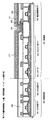
図6(A)は、EL素子の封止までを行った状態を示す上面図、図6(B)は図6(A)をA−A’で切断した断面図である。点線で示された601はソース側駆動回路、602は画素部、603はゲート側駆動回路である。また、604はカバー材、605は第1シール剤、606は第2シール剤であり、第1シール剤605で囲まれた内側は、空間になっている。
【0086】
なお、608はソース側駆動回路601及びゲート側駆動回路603に入力される信号を伝送するための配線であり、外部入力端子となるFPC(フレキシブルプリントサーキット)609からビデオ信号やクロック信号を受け取る。なお、ここではFPCしか図示されていないが、このFPCにはプリント配線基盤(PWB)が取り付けられていても良い。本明細書における発光装置には、発光装置本体だけでなく、それにFPCもしくはPWBが取り付けられた状態をも含むものとする。
【0087】
次に、断面構造について図6(B)を用いて説明する。基板610の上方には画素部602、ゲート側駆動回路603が形成されており、画素部602は電流制御用TFT611とそのドレインに電気的に接続された透明電極612を含む複数の画素により形成される。また、ゲート側駆動回路603はnチャネル型TFT613とpチャネル型TFT614とを組み合わせたCMOS回路(図5参照)を用いて形成される。
【0088】
透明電極612はEL素子の陽極として機能する。また、透明電極612の両端にはバンク615が形成され、透明電極612上にはEL層616およびEL素子の陰極617が形成される。
【0089】
陰極617は全画素に共通の配線としても機能し、接続配線608を経由してFPC609に電気的に接続されている。さらに、画素部602及びゲート側駆動回路603に含まれる素子は全て陰極617およびパッシベーション膜618で覆われている。
【0090】
また、第1シール剤605によりカバー材604が貼り合わされている。なお、カバー材604とEL素子との間隔を確保するために樹脂膜からなるスペーサを設けても良い。そして、第1シール剤605の内側の空間607には窒素といった不活性気体が充填されている。なお、第1シール剤605としてはエポキシ系樹脂を用いるのが好ましい。また、第1シール剤605はできるだけ水分や酸素を透過しない材料であることが望ましい。さらに、空間607の内部に吸湿効果をもつ物質や酸化を防止する効果をもつ物質を含有させても良い。
【0091】
また、本実施例ではカバー材604を構成するプラスチック基板の材料としてFRP(Fiberglass-Reinforced Plastics)、PVF(ポリビニルフロライド)、マイラー、ポリエステルまたはアクリルを用いることができる。
【0092】
また、第1シール剤605を用いてカバー材604を接着した後、さらに側面(露呈面)を覆うように第2シール剤606を設ける。なお、第2シール剤606は第1シール剤605と同じ材料を用いることができる。
【0093】
以上のような構造でEL素子を空間607に封入することにより、EL素子を外部から完全に遮断することができ、外部から水分や酸素等のEL層の酸化による劣化を促す物質が侵入することを防ぐことができる。従って、信頼性の高い発光装置を得ることができる。
【0094】
なお、本実施例の構成は、実施例1のいずれの構成とも自由に組み合わせて実施することが可能である。
【0095】
〔実施例3〕
ここで画素部のさらに詳細な上面構造を図7(A)に、回路図を図7(B)に示す。図7において、基板上に設けられたスイッチング用TFT704は図5のスイッチング用(nチャネル型)TFT503を用いて形成される。従って、構造の説明はスイッチング用(nチャネル型)TFT503の説明を参照すれば良い。また、703で示される配線は、スイッチング用TFT704のゲート電極704a、704bを電気的に接続するゲート配線である。
【0096】
なお、本実施例ではチャネル形成領域が二つ形成されるダブルゲート構造としているが、チャネル形成領域が一つ形成されるシングルゲート構造もしくは三つ形成されるトリプルゲート構造であっても良い。
【0097】
また、スイッチング用TFT704のソースはソース配線715に接続され、ドレインはドレイン配線705に接続される。また、ドレイン配線705は電流制御用TFT706のゲート電極707に電気的に接続される。なお、電流制御用TFT706は図5の電流制御用(pチャネル型)TFT504を用いて形成される。従って、構造の説明は電流制御用(pチャネル型)TFT504の説明を参照すれば良い。なお、本実施例ではシングルゲート構造としているが、ダブルゲート構造もしくはトリプルゲート構造であっても良い。
【0098】
また、電流制御用TFT706のソースは電流供給線716に電気的に接続され、ドレインはドレイン配線717に電気的に接続される。また、ドレイン配線717は点線で示される画素電極(陽極)718に電気的に接続される。
【0099】
このとき、719で示される領域には保持容量(コンデンサ)が形成される。コンデンサ719は、電流供給線716と電気的に接続された半導体膜720、ゲート絶縁膜と同一層の絶縁膜(図示せず)及びゲート電極707との間で形成される。また、ゲート電極707、第1層間絶縁膜と同一の層(図示せず)及び電流供給線716で形成される容量も保持容量として用いることが可能である。
【0100】
なお、本実施例の構成は、実施例1及び実施例2のいずれの構成とも自由に組み合わせて実施することが可能である。
【0101】
〔実施例4〕
本実施例では、実施例1で示したものとは異なる構造を有する発光装置の画素部について図8(A)回路図を示し、図8(B)に断面構造を示す。
【0102】
まず図8(A)において、801はスイッチング用TFT802のソースに接続されたソース信号線、また、803はスイッチング用TFT802のゲートに接続された書込用ゲート信号線である。さらに804は電流制御用TFTであり、805はコンデンサ(省略することも可能)である。また、806は電流供給線、807は消去用TFTであり、消去用ゲート信号線808に接続される。なお、809はEL素子であり、810は、対向電源である。消去用TFT807の動作については特願平11−338786号を参照すると良い。
【0103】
消去用TFT807のドレインは電流制御用TFT804のゲート電極に接続され、電流制御用TFT804のゲート電圧を強制的に変化させることができるようになっている。なお、消去用TFT807はnチャネル型TFTとしてもpチャネル型TFTとしても良いが、オフ電流を小さくできるようにスイッチング用TFT802と同一構造とすることが好ましい。
【0104】
次に断面構造について説明する。図8(B)において、基板800上に設けられたスイッチング用TFT802は公知の方法を用いて形成されたnチャネル型TFTを用いる。本実施例ではダブルゲート構造としている。ダブルゲート構造とすることで実質的に2つのTFTが直列された構造となり、オフ電流値を低減することができるという利点がある。また、公知の方法を用いて形成されたpチャネル型TFTを用いても構わない。
【0105】
次に、消去用TFT807は公知の方法を用いて形成されたnチャネル型TFTを用いる。なお、公知の方法を用いて形成されたpチャネル型TFTを用いても構わない。なお、消去用TFT807のドレイン配線826は別の配線によって、スイッチング用TFT802のドレイン配線816と、電流制御用TFTのゲート電極835(835a、835b)とに電気的に接続されている。
【0106】
また、本実施例において、スイッチング用TFT802および消去用TFT807の構造はいずれもゲート電極がゲート絶縁膜を介して低濃度不純物領域に重ならないように形成する。すなわちLDD領域を形成する。
【0107】
また、電流制御用TFT804は公知の方法を用いて形成されたpチャネル型TFTを用いる。電流制御用TFTのゲート電極835(835a、835b)は別の配線によって、スイッチング用TFT802のドレイン配線816と、消去用TFT807のドレイン配線826とに電気的に接続されている。
【0108】
なお、電流制御用TFT804の構造はいずれもゲート電極がゲート絶縁膜を介してソース領域およびドレイン領域に重ならないように形成される。
【0109】
また、本実施例では電流制御用TFT804をシングルゲート構造で図示しているが、複数のTFTを直列につなげたマルチゲート構造としても良い。さらに、複数のTFTを並列につなげて実質的にチャネル形成領域を複数に分割し、熱の放射を高い効率で行えるようにした構造としても良い。このような構造は熱による劣化対策として有効である。
【0110】
また、ドレイン配線836は電流供給線806に接続され、常に一定の電圧が加えられている。
【0111】
スイッチング用TFT802、電流制御用TFT804及び消去用TFT807の上には第1パッシベーション膜841が設けられ、その上に樹脂絶縁膜でなる層間絶縁膜842が形成される。層間絶縁膜842を用いてTFTによる段差を平坦化することは非常に重要である。後に形成されるEL層は非常に薄いため、段差が存在することによって発光不良を起こす場合がある。従って、EL層をできるだけ平坦面に形成しうるように画素電極を形成する前に平坦化しておくことが望ましい。
【0112】
また、画素電極(陽極)843として透明導電膜を用いる。具体的には酸化インジウムと酸化亜鉛との化合物でなる導電膜を用いる。勿論、酸化インジウムと酸化スズとの化合物でなる導電膜を用いても良い。
なお、電流制御用TFT804のドレイン領域に電気的に接続される。
【0113】
また、絶縁膜(好ましくは樹脂)で形成されたバンク844a、844bにより形成された溝(画素に相当する)の中にEL層845が形成される。なお、ここでは一画素しか図示していないが、R(赤)、G(緑)、B(青)の各色に対応したEL層を作り分けても良い。EL層を形成する有機EL材料としてはπ共役ポリマー系材料を用いる。代表的なポリマー系材料としては、ポリパラフェニレンビニレン(PPV)系、ポリビニルカルバゾール(PVK)系、ポリフルオレン系などが挙げられる。
【0114】
なお、PPV系有機EL材料としては様々な型のものがあるが、例えば「H. Shenk,H.Becker,O.Gelsen,E.Kluge,W.Kreuder,and H.Spreitzer,“Polymers for Light Emitting Diodes”,Euro Display,Proceedings,1999,p.33-37」や特開平10−92576号公報に記載されたような材料を用いれば良い。
【0115】
なお、本実施例では、赤色に発光する発光層にはシアノポリフェニレンビニレン、緑色に発光する発光層にはポリフェニレンビニレン、青色に発光する発光層にはポリフェニレンビニレン若しくはポリアルキルフェニレンを用いれば良い。膜厚は30〜150nm(好ましくは40〜100nm)とすれば良い。
【0116】
但し、以上の例はEL層を形成する発光層に用いることのできる有機EL材料の一例であって、これに限定する必要はまったくない。本発明においては、正孔注入層、正孔輸送層、発光層、電子輸送層、電子注入層、正孔阻止層およびバッファー層といった異なる機能を有する材料からなる層を自由に組み合わせてEL層(発光及びそのためのキャリアの移動を行わせるための層)を形成すれば良い。
【0117】
例えば、本実施例ではポリマー系材料を発光層として用いる例を示したが、低分子系有機EL材料を用いても良い。また、電荷輸送層や電荷注入層として炭化珪素等の無機材料を用いることも可能である。これらの有機EL材料や無機材料は公知の材料を用いることができる。
【0118】
EL層845の上には、陰極846が形成される。なお、陰極846は、MgAgにより形成される。
【0119】
陰極846まで形成された時点でEL素子810が完成する。なお、ここでいうEL素子810は、画素電極(陽極)843、発光層845、及び陰極846で形成された素子を指す。
【0120】
また本実施例では、陰極846の上にさらにアルミニウムでなる保護電極847を形成し、さらにその上にパッシベーション膜848を設けている。パッシベーション膜848としては窒化珪素膜または窒化酸化珪素膜が好ましい。この目的は、外部とEL素子とを遮断することであり、有機EL材料の酸化による劣化を防ぐ意味と、有機EL材料からの脱ガスを抑える意味との両方を併せ持つ。これにより発光装置の信頼性が高められる。
【0121】
以上のように本発明の発光装置は図8のような構造からなり、オフ電流値の十分に低いスイッチング用TFTと、ホットキャリア注入に強い電流制御用TFTとを有する。従って、高い信頼性を有し、且つ、良好な画像表示が可能な発光装置が得られる。なお、本実施例において、画素部の構造に関してのみ説明したが、駆動回路に関しては、実施例1に示したものと同じ構成とする。
【0122】
なお、本実施例の構成は、実施例1〜実施例3のいずれの構成とも自由に組み合わせて実施することが可能である。
【0123】
〔実施例5〕
次に、実施例4とは異なる構成で本発明を実施した発光装置の画素部の回路図を図9(A)に示し、画素部の断面構造を図9(B)に示す。
なお、駆動方法等の詳細については、特願2000−127384号を参照すればよい。
【0124】
まず図9(A)において、901はスイッチング用TFT902のソースに接続されたソース信号線、また、903はスイッチング用TFT902のゲート電極に接続された書込用ゲート信号線である。さらに904(904a、904b)は電流制御用TFTであり、905はコンデンサ(省略することも可能)である。また、906は電流供給線、907は消去用TFTであり、消去用ゲート信号線908に接続される。なお、909はEL素子であり、910は、対向電源である。
【0125】
消去用TFT907のドレインは電流制御用TFT904のゲート電極に接続され、電流制御用TFT904のゲート電圧を強制的に変化させることができるようになっている。なお、消去用TFT907はnチャネル型TFTとしてもpチャネル型TFTとしても良いが、オフ電流を小さくできるようにスイッチング用TFT902と同一構造とすることが好ましい。
【0126】
また本実施例では電流制御用TFT904として、第1の電流制御用TFT904aと第2の電流制御用TFT904bとが並列に設けられている。これによって、電流制御用TFTの活性層を流れる電流によって発生した熱の放射を効率的に行うことができ、電流制御用TFTの劣化を抑えることができる。また、電流制御用TFTのしきい値や移動度などの特性のばらつきによって生じるドレイン電流のばらつきを抑えることができる。
【0127】
なお本実施例では電流制御用TFTとして、第1の電流制御用TFT904aと第2の電流制御用TFT904bを用いたが、本実施例はこれに限定されない。各画素において、電流制御用TFTとして用いるTFTの数は、2つ以上であれば良い。
【0128】
また、本実施例における発光装置の断面図を図9(B)に示すが実施例3で示したものとほとんど同じ構造であるので説明を省略するが、図9(A)の説明の際にふれたように電流制御用TFTが2つあり、なおかつ並列に形成されているのが特徴であり、これについて説明する。
【0129】
図9(B)において、電流制御用TFT904は、第1の電流制御用TFT904a及び第2の電流制御用TFT904bを有する。なお、第1の電流制御用TFT904aのドレイン932aは、ドレイン配線936aを介してEL素子909の画素電極943と電気的に接続されている。また、第2の電流制御用TFT904bのドレイン932bも同様にドレイン配線936bを介してEL素子909の画素電極943と電気的に接続されている。なお、第1の電流制御用TFT904aおよび第2の電流制御用TFT904bの構造はいずれもゲート電極がゲート絶縁膜を介してソース領域およびドレイン領域に重ならないように形成される。
【0130】
また、第1の電流制御用TFT904aのゲート電極934(934a、934b)および第2の電流制御用TFT904bのゲート電極935(935a、935b)は、スイッチング用TFT902のドレイン912とドレイン配線916を介して電気的に接続されている。なお、消去用TFT907のドレイン922とドレイン配線926を介して電気的に接続されている。
【0131】
なお、本実施例において、スイッチング用TFT902および消去用TFT907の構造はいずれもゲート電極がゲート絶縁膜を介して低濃度不純物領域に重ならないように形成される。
【0132】
なお、本実施例において、画素部の構造に関してのみ説明したが、駆動回路に関しては、実施例1に示したものと同じ構成とする。
また、本実施例の構成は、実施例1〜実施例4のいずれの構成とも自由に組み合わせて実施することが可能である。
【0133】
〔実施例6〕
本発明の発光装置を駆動するにあたって、画像信号としてアナログ信号を用いたアナログ駆動を行うこともできるし、デジタル信号を用いたデジタル駆動を行うこともできる。
【0134】
アナログ駆動を行う場合、スイッチング用TFTのソース配線にはアナログ信号が送られ、その階調情報を含んだアナログ信号が電流制御用TFTのゲート電圧となる。そして、電流制御用TFTでEL素子に流れる電流を制御し、EL素子の発光強度を制御して階調表示を行う。なお、アナログ駆動を行う場合は電流制御用TFTを飽和領域で動作させると良い。
【0135】
一方、デジタル駆動を行う場合、アナログ的な階調表示とは異なり、時分割駆動と呼ばれる階調表示を行う。即ち、発光時間の長さを調節することで、視覚的に色階調が変化しているように見せる。なお、デジタル駆動を行う場合は電流制御用TFTを線形領域で動作させると良い。
【0136】
EL素子は液晶素子に比べて非常に応答速度が速いため、高速で駆動することが可能である。そのため、1フレームを複数のサブフレームに分割して階調表示を行う時分割駆動に適した素子であると言える。
【0137】
このように、本発明は素子構造に関する技術であるので、駆動方法は如何なるものであっても構わない。
【0138】
なお、本実施例の構成は、実施例1〜実施例5のいずれの構成とも自由に組み合わせて実施することが可能である。
【0139】
〔実施例7〕
本発明の発光装置は、自発光型であるため液晶ディスプレイに比べて明るい場所での視認性に優れ、しかも視野角が広い。従って、様々な電気器具の表示部として用いることができる。例えば、TV放送等を大画面で鑑賞するには対角30インチ以上(典型的には40インチ以上)の表示装置の表示部において本発明の発光装置を用いると良い。
【0140】
なお、表示装置には、パソコン用表示装置、TV放送受信用表示装置、広告表示用表示装置等の全ての情報表示用表示装置が含まれる。また、その他にも様々な電気器具の表示部に本発明の発光装置を用いることができる。
【0141】
その様な本発明の電気器具としては、ビデオカメラ、デジタルカメラ、ゴーグル型表示装置(ヘッドマウントディスプレイ)、ナビゲーションシステム、音響再生装置(カーオーディオ、オーディオコンポ等)、ノート型パーソナルコンピュータ、ゲーム機器、携帯情報端末(モバイルコンピュータ、携帯電話、携帯型ゲーム機または電子書籍等)、記録媒体を備えた画像再生装置(具体的にはデジタルビデオディスク(DVD)等の記録媒体を再生し、その画像を表示しうるディスプレイを備えた装置)などが挙げられる。特に、斜め方向から見ることの多い携帯情報端末は視野角の広さが重要視されるため、発光装置を用いることが望ましい。それら電気器具の具体例を図10および図11に示す。
【0142】
図10(A)は表示装置であり、筐体1001、支持台1002、表示部1003等を含む。本発明の発光装置は表示部1003にて用いることができる。なお、本発明の発光装置は自発光型であるためバックライトが必要なく、液晶ディスプレイよりも薄い表示部とすることができる。
【0143】
図10(B)はビデオカメラであり、本体1011、表示部1012、音声入力部1013、操作スイッチ1014、バッテリー1015、受像部1016等を含む。本発明の発光装置は表示部1012にて用いることができる。
【0144】
図10(C)はヘッドマウントディスプレイの一部(右片側)であり、本体1021、信号ケーブル1022、頭部固定バンド1023、表示部1024、光学系1025、表示装置1026等を含む。本発明の発光装置は表示装置1026にて用いることができる。
【0145】
図10(D)は記録媒体を備えた画像再生装置(具体的にはDVD再生装置)であり、本体1031、記録媒体(DVD等)1032、操作スイッチ1033、表示部(a)1034、表示部(b)1035等を含む。表示部(a)1034は主として画像情報を表示し、表示部(b)1035は主として文字情報を表示するが、本発明の発光装置はこれら表示部(a)1034、表示部(b)1035にて用いることができる。なお、記録媒体を備えた画像再生装置には家庭用ゲーム機器なども含まれる。
【0146】
図10(E)はゴーグル型表示装置(ヘッドマウントディスプレイ)であり、本体1041、表示部1042、アーム部1043を含む。本発明の発光装置は表示部1042にて用いることができる。
【0147】
図10(F)はパーソナルコンピュータであり、本体1051、筐体1052、表示部1053、キーボード1054等を含む。本発明の発光装置は表示部1053にて用いることができる。
【0148】
なお、将来的にEL材料の発光輝度が高くなれば、出力した画像情報を含む光をレンズ等で拡大投影してフロント型あるいはリア型のプロジェクターに用いることも可能となる。
【0149】
また、上記電気器具はインターネットやCATV(ケーブルテレビ)などの電子通信回線を通じて配信された情報を表示することが多くなり、特に動画情報を表示する機会が増してきている。EL材料の応答速度は非常に高いため、本発明の発光装置は動画表示に好ましい。
【0150】
図11(A)は携帯電話であり、本体1101、音声出力部1102、音声入力部1103、表示部1104、操作スイッチ1105、アンテナ1106を含む。本発明の発光装置は表示部1104にて用いることができる。なお、表示部1104は黒色の背景に白色の文字を表示することで携帯電話の消費電力を抑えることができる。
【0151】
図11(B)は音響再生装置、具体的にはカーオーディオであり、本体1111、表示部1112、操作スイッチ1113、1114を含む。本発明の発光装置は表示部1112にて用いることができる。また、本実施例では車載用オーディオを示すが、携帯型や家庭用の音響再生装置に用いても良い。なお、表示部1112は黒色の背景に白色の文字を表示することで消費電力を抑えられる。これは携帯型の音響再生装置において特に有効である。
【0152】
図11(C)はデジタルカメラであり、本体1121、表示部(A)1122、接眼部1123、操作スイッチ1124、表示部(B)1125、バッテリー1126を含む。本発明の発光装置は、表示部(A)1122、表示部(B)1125にて用いることができる。また、表示部(B)1125を、主に操作用パネルとして用いる場合、黒色の背景に白色の文字を表示することで消費電力を抑えることができる。
【0153】
また、本実施例にて示した携帯型電気器具においては、消費電力を低減するための方法としては、外部の明るさを感知するセンサ部を設け、暗い場所で使用する際には、表示部の輝度を落とすなどの機能を付加するなどといった方法が挙げられる。
【0154】
以上の様に、本発明の適用範囲は極めて広く、あらゆる分野の電気器具に用いることが可能である。また、本実施例の電気器具は実施例1〜実施例6に示したいずれの構成を適用しても良い。
【0155】
【発明の効果】
本発明を実施することにより、発光装置の駆動回路および画素部において、ゲート電極と低濃度不純物領域における構造の異なるTFTを作製することができる。これにより駆動回路のTFTに期待されるオン電流の向上およびホットキャリア対策、さらに画素部のTFTに期待されるオフ電流の低下という課題を一度に解決することができる。さらに、画素部におけるpチャネル型TFTの作製時に生じていたプロセス上の問題点を解決することができる。
【図面の簡単な説明】
【図1】 本発明の実施の形態を説明する図。
【図2】 本発明の発光装置の作製行程を示す図。
【図3】 本発明の発光装置の作製行程を示す図。
【図4】 本発明の発光装置の作製行程を示す図。
【図5】 本発明の発光装置の作製行程を示す図。
【図6】 本発明の発光装置の封止構造を示す図。
【図7】 本発明の発光装置の画素部の上面構造及び回路図。
【図8】 本発明の発光装置の画素部の回路図及び断面図。
【図9】 本発明の発光装置の画素部の回路図及び断面図。
【図10】 本発明の発光装置を用いた電気器具の具体例を示す図。
【図11】 本発明の発光装置を用いた電気器具の具体例を示す図。[0001]
BACKGROUND OF THE INVENTION
The present invention relates to a light emitting device having a circuit formed of a thin film transistor (hereinafter referred to as TFT) and a manufacturing method thereof. Note that a light-emitting device in this specification refers to a device such as an image display device having a light-emitting element that can emit light by applying an electric field. In addition, connectors such as anisotropic conductive film ((FPC: flexible printed circuit) or TAB (Tape Automated Bonding) tape or TCP (Tape Carrier Package)) are attached to the light emitting element, printed on the end of TAB tape or TCP. In addition to modules with a wiring board or modules in which an IC (integrated circuit) is directly mounted on a light-emitting element by the COG (Chip On Glass) method, the light-emitting device also includes electric appliances with the light-emitting device as a component. Is included.
[0002]
[Prior art]
In recent years, a technology for forming a TFT on a substrate has greatly advanced, and application development to an active matrix display device has been advanced. In particular, a TFT using a polysilicon film has higher field effect mobility (also referred to as mobility) than a conventional TFT using an amorphous silicon film, and thus can operate at high speed. For this reason, it is possible to control a pixel, which has been conventionally performed by a drive circuit outside the substrate, with a drive circuit formed on the same substrate as the pixel.
[0003]
Such an active matrix display device has various advantages such as a reduction in manufacturing cost, a reduction in size of an electro-optical device, an increase in yield, and a reduction in throughput by forming various circuits and elements on the same substrate. can get.
[0004]
In addition, research on active matrix light-emitting devices having EL elements as self-luminous elements has been actively conducted.
[0005]
Note that the EL element in this specification has a structure in which an EL layer is sandwiched between a pair of electrodes (anode and cathode), but the EL layer usually has a laminated structure. A typical example is a “hole transport layer / light emitting layer / electron transport layer” stacked structure proposed by Tang et al. Of Kodak Eastman Company. This structure has very high luminous efficiency, and most of the light emitting devices that are currently under research and development employ this structure.
[0006]
In addition, the hole injection layer / hole transport layer / light emitting layer / electron transport layer, or hole injection layer / hole transport layer / light emitting layer / electron transport layer / electron injection layer are laminated in this order on the anode. Structure may be sufficient. It is also possible to dope the light emitting layer with a fluorescent dye or the like.
[0007]
In this specification, all layers provided between a cathode and an anode are collectively referred to as an EL layer. Therefore, the above-described hole injection layer, hole transport layer, light emitting layer, electron transport layer, electron injection layer, and the like are all included in the EL layer.
[0008]
Then, a predetermined voltage is applied to the EL layer having the above structure from the pair of electrodes, whereby recombination of carriers occurs in the light emitting layer to emit light. Note that the light emission obtained here includes fluorescence and phosphorescence. In this specification, a light-emitting element formed using an anode, an EL layer, and a cathode is referred to as an EL element.
[0009]
Since an EL layer included in an EL element is accelerated by heat, light, moisture, oxygen, or the like, generally, in manufacturing an active matrix light-emitting device, an EL element is formed after a wiring or a TFT is formed in a pixel portion. It is formed.
[0010]
In an active matrix light emitting device, a switching element made of a TFT is provided for each pixel, and a driving element (current control TFT) that controls current is operated by the switching element (switching TFT) to operate an EL layer (light emitting layer). ). For example, there is a light emitting device described in JP-A-10-189252.
[0011]
Note that switching TFT and current control TFT in the pixel section
Requires a low off-state current (Ioff). As a TFT structure for reducing off current, a structure in which a gate electrode has a region (LDD region) that does not overlap with a low concentration impurity region through a gate insulating film is known.
[0012]
On the other hand, an image circuit that performs image display and a drive circuit for controlling the image circuit are required to improve reliability by preventing deterioration due to a high drive capability (on current: Ion) and a hot carrier effect. Yes. As a structure effective for preventing deterioration of the on-current value due to hot carriers, a structure in which a gate electrode has a region (GOLD region) overlapping with a low-concentration impurity region through a gate insulating film is known.
[0013]
[Problems to be solved by the invention]
However, if a TFT having an LDD region or a TFT having a GOLD region is formed, the manufacturing process becomes complicated. In the present invention, in an active matrix light-emitting device, a TFT used in a driver circuit thereof has high driving capability (on current) and reliability, while a TFT used in a pixel portion has low off current. It is another object of the present invention to realize this manufacturing process with a small number of masks.
[0014]
[Means for Solving the Invention]
In the present invention, among TFTs formed over the same substrate, an n-channel TFT used for a driver circuit is manufactured with a structure having a low concentration impurity region (GOLD region) at a position overlapping with a gate electrode made of a conductive layer. On the other hand, an n-channel TFT used for a pixel portion is manufactured with a structure having a low-concentration impurity region (LDD region) at a position not overlapping with a gate electrode.
[0015]
A TFT having a GOLD region has a structure suitable for preventing deterioration due to hot carrier injection in the TFT, and a structure suitable for a driver circuit because of high on-current.
[0016]
A TFT having an LDD region has a structure in which off-state current is low, and thus has a structure suitable as a TFT in a pixel portion.
[0017]
Further, the p-channel TFT is manufactured by doping an impurity region of the n-channel TFT. Note that when doping is performed using an n-channel TFT having an LDD region at this time, variation in impurity concentration due to the film thickness of the gate electrode, which is generated when an n-channel TFT having a GOLD region is doped, can be suppressed.
[0018]
Therefore, a light-emitting device including a TFT suitable for a driver circuit and a pixel portion can be manufactured by forming the TFT having the above structure over the same substrate.
[0019]
DETAILED DESCRIPTION OF THE INVENTION
An embodiment of the present invention will be described in detail with reference to FIG. In FIG. 1A, reference numeral 102 denotes a semiconductor layer made of Si, and a gate electrode made of a conductive layer is formed in part of the semiconductor layer. Here, the gate electrode 1 (104) made of TaN and the gate electrode 2 (105) made of W have a laminated structure, and the gate insulating film made of an insulating film containing silicon using the gate electrode as a mask. By doping an impurity (phosphorus) through 103, a high concentration impurity region 106 is formed. Note that the high concentration impurity region 106 finally becomes a source region and a drain region of the n-channel TFT.
[0020]
Then, the low concentration impurity region a (107) is formed by doping the impurity (phosphorus) again. However, the impurity concentration in the low concentration impurity region a (107) is formed to be lower than that in the previous high concentration impurity region (FIG. 1B). Such a low concentration impurity region is referred to as an LDD (Lightly Doped Drain) region. The low concentration impurity region a (107) formed here is called a GOLD (Gate-drain Overlapped LDD) region because it overlaps with the gate electrode through the gate insulating film.
[0021]
Next, an etching process is performed. At this time, the TFT in which the gate electrode 1 (104) is etched has a structure shown in FIG. Specifically, the impurity region b (107) formed in a position overlapping with the gate electrode 1 (104) in FIG. 1B is etched by etching the gate electrode 1 (104). 104) and a low concentration impurity region b (108) which does not overlap.
[0022]
On the other hand, when the mask is formed so that the gate electrode 1 (104) is not etched, the structure of FIG. 1D having the low concentration impurity region a (107) can be formed.
[0023]
Then, when the gate insulating film 103 is etched as a whole, the impurity region 106 is exposed as shown in FIGS. 1E and 1F, and n-channel TFTs having different structures are formed on the same substrate. Can be formed.
[0024]
Note that the n-channel TFT having the structure illustrated in FIG. 1C is used for the pixel portion because the low-concentration impurity region has a region where the gate electrode does not overlap (LDD region), so that off-state current can be reduced. In addition, since the n-channel TFT having the structure illustrated in FIG. 1D has a structure (GOLD region) in which a low-concentration impurity region overlaps with a gate electrode, on-state current can be increased and deterioration due to hot carriers can be prevented. Therefore, it is used for a driving circuit.
[0025]
Further, an n-channel TFT having the structure shown in FIG. 1E is doped with an impurity (boron) to manufacture a p-channel TFT. At this time, since the impurity (boron) is doped through the gate insulating film 103 on Si if it has the structure of FIG. 1E, the n-channel type of the structure shown in FIG. It is possible to prevent variations in the impurity doping amount due to the TaN film thickness of the gate electrode 1 (104), which occurs when the TFT is doped with impurities (boron). That is, a p-channel TFT having a uniform impurity concentration in the impurity region can be manufactured.
[0026]
Note that the p-channel TFT manufactured here is used for a driver circuit and a pixel portion. However, the p-channel TFT in the driver circuit is not limited to this, and a p-channel TFT manufactured by doping an impurity (boron) into the n-channel TFT having the structure shown in FIG. Also good.
[0027]
Examples of the present invention will be described below. The following examples are preferred examples, and the light-emitting device of the present invention is not limited to the following examples.
[0028]
【Example】
[Example 1]
Here, a detailed description is given of a method for simultaneously manufacturing a pixel portion and TFTs of a driver circuit (n-channel TFT and p-channel TFT) provided on the periphery of the pixel portion on the same substrate by implementing the present invention. 5 will be described.
[0029]
First, in this embodiment, a
[0030]
Next, a
[0031]
Next, semiconductor layers 302 to 305 are formed over the base film. The semiconductor layers 302 to 305 are formed by forming a semiconductor film having an amorphous structure by a known means (a sputtering method, an LPCVD method, a plasma CVD method, or the like), and then performing a known crystallization process (laser crystallization method, heat A crystalline semiconductor film obtained by performing a crystallization method or a thermal crystallization method using a catalyst such as nickel) is formed by patterning into a desired shape. The semiconductor layers 302 to 305 are formed to have a thickness of 25 to 80 nm (preferably 30 to 60 nm). The material of the crystalline semiconductor film is not limited, but is preferably silicon (silicon) or silicon germanium (Si X Ge 1-X (X = 0.0001 to 0.02)) It may be formed of an alloy or the like. In this example, a 55 nm amorphous silicon film was formed by plasma CVD, and then a solution containing nickel was held on the amorphous silicon film. This amorphous silicon film is dehydrogenated (500 ° C., 1 hour), then thermally crystallized (550 ° C., 4 hours), and further laser annealed to improve crystallization. Thus, a crystalline silicon film was formed. Then, semiconductor layers 302 to 305 were formed by patterning the crystalline silicon film using a photolithography method.
[0032]
Further, after forming the semiconductor layers 302 to 305, a small amount of impurity element (boron or phosphorus) may be doped in order to control the threshold value of the TFT.
[0033]
When a crystalline semiconductor film is formed by laser crystallization, a pulse oscillation type or continuous emission type excimer laser, YAG laser, YVO Four A laser can be used. When these lasers are used, it is preferable to use a method in which laser light emitted from a laser oscillator is linearly collected by an optical system and irradiated onto a semiconductor film. Crystallization conditions are appropriately selected by the practitioner. When an excimer laser is used, the pulse oscillation frequency is 300 Hz, and the laser energy density is 100 to 400 mJ / cm 2 (typically 200 to 300 mJ / cm 2). 2 ). When a YAG laser is used, the second harmonic is used and the pulse oscillation frequency is set to 30 to 300 Hz, and the laser energy density is set to 300 to 600 mJ / cm. 2 (Typically 350-500mJ / cm 2 ) Then, when the laser beam condensed linearly with a width of 100 to 1000 μm, for example, 400 μm is irradiated over the entire surface of the substrate, the superposition ratio (overlap ratio) of the linear laser light at this time is 50 to 90%. Good.
[0034]
Next, a
[0035]
When a silicon oxide film is used, TEOS (Tetraethyl Orthosilicate) and O 2 The reaction pressure is 40 Pa, the substrate temperature is 300 to 400 ° C., and the high frequency (13.56 MHz) power density is 0.5 to 0.8 W / cm. 2 And can be formed by discharging. The silicon oxide film thus manufactured can obtain good characteristics as a gate insulating film by thermal annealing at 400 to 500 ° C. thereafter.
[0036]
Next, as illustrated in FIG. 2A, a first
[0037]
In this embodiment, the first
[0038]
Next, as shown in FIG. 2B, resist
[0039]
After that, as shown in FIG. 2B, the resist
[0040]
In the first etching process, the shape of the mask made of resist is made suitable, and the end portions of the first conductive layer and the second conductive layer are tapered due to the effect of the bias voltage applied to the substrate side. It becomes. The angle of the tapered portion may be 15 to 45 °. Thus, the first shape conductive layers 314 to 318 (first
[0041]
Then, a first doping process is performed without removing the resist mask, and an impurity element imparting n-type conductivity is added to the semiconductor layer. (FIG. 2B) The doping process may be performed by an ion doping method or an ion implantation method. The condition of the ion doping method is a dose of 1 × 10 13 ~ 5x10 15 atoms / cm 2 The acceleration voltage is set to 60 to 100 keV. In this embodiment, the dose is 1.5 × 10 15 atoms / cm 2 The acceleration voltage was 80 keV. As an impurity element imparting n-type, an element belonging to Group 15, typically phosphorus (P) or arsenic (As), is used here, but phosphorus (P) is used. In this case, the conductive layers 314 to 318 serve as a mask for the impurity element imparting n-type, and the high
[0042]
Next, as shown in FIG. 2C, a second etching process is performed without removing the resist mask. Here, CF is used as an etching gas. Four And Cl 2 And O 2 Each gas flow rate ratio was 20/20/20 (sccm), 500 W RF (13.56 MHz) power was applied to the coil-type electrode at a pressure of 1 Pa, and plasma was generated to perform etching. . 20 W RF (13.56 MHz) power is also applied to the substrate side (sample stage), and a substantially negative self-bias voltage is applied. In the second etching process, the etching rate with respect to W is 124.62 nm / min, the etching rate with respect to TaN is 20.67 nm / min, and the selection ratio of W with respect to TaN is 6.05. Therefore, the W film is selectively etched. By this second etching, the taper angle of W became 70 °. Second
[0043]
Next, a second doping process is performed. Doping is performed using the second
[0044]
Next, as shown in FIG. 3B, a resist mask is removed, and then a third etching process is performed using a photolithography method. In the third etching process, the tapered portion of the first conductive layer is partially etched to form a shape overlapping the second conductive layer. However, a mask made of resist (338, 339) is formed in a region where the third etching is not performed, as shown in FIG.
[0045]
The etching conditions in the third etching process are Cl as an etching gas. 2 And SF 6 And the respective gas flow ratios are set to 10/50 (sccm) using the ICP etching method in the same manner as the first and second etchings. Note that the etching rate for TaN in the third etching process is 111.2 nm / min, and the etching rate for the gate insulating film is 12.8 nm / min.
[0046]
In this example, etching was performed by generating plasma by applying 500 W of RF (13.56 MHz) power to the coil-type electrode at a pressure of 1.3 Pa. 10 W RF (13.56 MHz) power is also applied to the substrate side (sample stage), and a substantially negative self-bias voltage is applied. Through the above steps, the first
[0047]
By the third etching, impurity regions (LDD regions) 343 to 345 that do not overlap with the first
[0048]
In addition, the electrode formed by the first
[0049]
Similarly, the electrode formed by the first conductive layer 341a and the second conductive layer 341b finally becomes the gate electrode of the n-channel TFT in the pixel portion, and the first
[0050]
Thus, in this embodiment, the impurity regions (LDD regions) 343 to 345 that do not overlap with the first
[0051]
Next, as shown in FIG. 3C, the
[0052]
Next, after removing the resist mask, new resist
[0053]
In this embodiment, the
[0054]
Through the above steps, impurity regions are formed in the respective semiconductor layers.
Note that although a method for doping impurities (boron) after etching the gate insulating film is described in this embodiment, the doping may be performed before the gate insulating film is etched.
[0055]
Next, the resist
[0056]
Next, a step of activating the impurity element added to each semiconductor layer is performed. This activation process is performed by a thermal annealing method using a furnace annealing furnace. As the thermal annealing method, it may be performed at 400 to 700 ° C., typically 500 to 550 ° C. in a nitrogen atmosphere having an oxygen concentration of 1 ppm or less, preferably 0.1 ppm or less. The activation treatment was performed by heat treatment. In addition to the thermal annealing method, a laser annealing method or a rapid thermal annealing method (RTA method) can be applied.
[0057]
In this embodiment, at the same time as the activation treatment, nickel used as a catalyst during crystallization is gettered to impurity regions (334 to 337, 350, 352) containing high-concentration phosphorus, and mainly the channel. The nickel concentration in the semiconductor layer that becomes the formation region is reduced. A TFT having a channel formation region manufactured in this manner has a low off-current value and good crystallinity, so that high field-effect mobility can be obtained and good characteristics can be achieved.
[0058]
In addition, an activation process may be performed before forming the first interlayer insulating film. However, when the wiring material used is weak against heat, it is activated after an interlayer insulating film (insulating film containing silicon as a main component, for example, a silicon nitride film) is formed to protect the wiring and the like as in this embodiment. It is preferable to perform the conversion treatment.
[0059]
In addition, the first interlayer insulating film may be formed by performing a doping process after the activation process.
[0060]
Furthermore, a heat treatment is performed at 300 to 550 ° C. for 1 to 12 hours in an atmosphere containing 3 to 100% hydrogen to perform a step of hydrogenating the semiconductor layer. In this embodiment, heat treatment was performed at 410 ° C. for 1 hour in a nitrogen atmosphere containing about 3% hydrogen. This step is a step of terminating dangling bonds in the semiconductor layer with hydrogen contained in the interlayer insulating film. As another means of hydrogenation, plasma hydrogenation (using hydrogen excited by plasma) may be performed.
[0061]
In the case where a laser annealing method is used as the activation treatment, it is desirable to irradiate a laser beam such as an excimer laser or a YAG laser after performing the hydrogenation.
[0062]
Next, as shown in FIG. 4C, a second
[0063]
As the second
[0064]
In this embodiment, a silicon oxynitride film formed by plasma CVD is formed. Note that the thickness of the silicon oxynitride film is preferably 1 to 5 μm (more preferably 2 to 4 μm). A silicon oxynitride film is effective in suppressing deterioration of an EL element because it contains a small amount of moisture.
In addition, although dry etching or wet etching can be used for forming the contact hole, it is desirable to use the wet etching method in view of the problem of electrostatic breakdown during etching.
[0065]
Further, since the first interlayer insulating film and the second interlayer insulating film are simultaneously etched in the formation of the contact hole here, considering the shape of the contact hole, the material for forming the second interlayer insulating film is the first interlayer insulating film. It is preferable to use a material having a higher etching rate than the material forming the film.
[0066]
Then, wirings 359 to 366 that are electrically connected to the
[0067]
Next, a transparent conductive film is formed thereon with a thickness of 80 to 120 nm, and a
In this embodiment, an indium tin oxide (ITO) film or a transparent conductive film in which 2 to 20% zinc oxide (ZnO) is mixed with indium oxide is used as the transparent electrode.
[0068]
Further, the
[0069]
Next, as shown in FIG. 5, an insulating film containing silicon (silicon oxide film in this embodiment) is formed to a thickness of 500 [nm], and an opening is formed at a position corresponding to the
[0070]
In this embodiment, a film made of silicon oxide is used as the third interlayer insulating film. However, an organic resin film such as polyimide, polyamide, acrylic, or BCB (benzocyclobutene) may be used in some cases. it can.
[0071]
Next, an
[0072]
Note that a known material can be used for the
[0073]
In this embodiment, polyphenylene vinylene is formed by a vapor deposition method as a hole transport layer. The light-emitting layer is formed by vapor deposition of 30-40% PBD of 1,3,4-oxadiazole derivative in polyvinyl carbazole, and about 1% of coumarin 6 is used as a green emission center. It is added.
[0074]
The
[0075]
The
[0076]
Note that the thickness of the
[0077]
Thus, an EL module having a structure as shown in FIG. 5 is completed. In addition, in the manufacturing process of the EL module in this embodiment, the source signal line is formed by Ta and W, which are materials forming the gate electrode, and the source and drain electrodes are formed due to the circuit configuration and the process. Although the gate signal line is formed of Al which is the wiring material being used, a different material may be used.
[0078]
In addition, a driver circuit 506 including an n-channel TFT 501 and a p-channel TFT 502, and a pixel portion 507 including a switching TFT 503, a current control TFT 504, and a capacitor 505 can be formed over the same substrate.
[0079]
In this embodiment, since the EL element configuration is bottom emission, an n-channel TFT is used as the switching TFT 503 and a p-channel TFT is used as the current control TFT 504. However, this is only a preferred form and need not be limited to this.
[0080]
The n-channel TFT 501 of the driver circuit 506 includes a
[0081]
The switching TFT 503 of the pixel portion 507 does not overlap with the channel formation region 374 and the first conductive layer 341a for forming the gate electrode, but the low concentration impurity region 344 (LDD region) and the source region formed outside the gate electrode. Alternatively, a high
[0082]
The current control TFT 504 in the pixel portion 507 includes a channel formation region 375 and high-
[0083]
In this embodiment, the structure in which the EL layer is formed on the pixel electrode (anode) and then the cathode is formed is shown, but the structure in which the EL layer and the anode are formed on the pixel electrode (cathode) is also possible. good. However, in this case, unlike the bottom emission described so far, the top emission is used. At this time, the switching TFT and the current control TFT are preferably formed of n-channel TFTs having the low-concentration impurity regions (LDD regions) described in this embodiment.
[0084]
[Example 2]
In this example, a method for completing the EL module (FIG. 5) manufactured in Example 1 as a light-emitting device will be described with reference to FIGS.
[0085]
6A is a top view illustrating a state where the EL element is sealed, and FIG. 6B is a cross-sectional view taken along line AA ′ in FIG. 6A. 601 indicated by a dotted line is a source side driver circuit, 602 is a pixel portion, and 603 is a gate side driver circuit. Further, 604 is a cover material, 605 is a first sealing agent, 606 is a second sealing agent, and the inside surrounded by the first sealing agent 605 is a space.
[0086]
Reference numeral 608 denotes a wiring for transmitting signals input to the source side driver circuit 601 and the gate side driver circuit 603, and receives a video signal and a clock signal from an FPC (flexible printed circuit) 609 serving as an external input terminal. Although only the FPC is shown here, a printed wiring board (PWB) may be attached to the FPC. The light-emitting device in this specification includes not only a light-emitting device body but also a state in which an FPC or a PWB is attached thereto.
[0087]
Next, a cross-sectional structure will be described with reference to FIG. A pixel portion 602 and a gate side driver circuit 603 are formed above the substrate 610. The pixel portion 602 is formed by a plurality of pixels including a
[0088]
The transparent electrode 612 functions as an anode of the EL element. Further, banks 615 are formed at both ends of the transparent electrode 612, and an EL layer 616 and an EL element cathode 617 are formed on the transparent electrode 612.
[0089]
The cathode 617 also functions as a wiring common to all pixels, and is electrically connected to the
[0090]
Further, a cover material 604 is bonded to the first sealant 605. Note that a spacer made of a resin film may be provided in order to secure a gap between the cover material 604 and the EL element. The space 607 inside the first sealant 605 is filled with an inert gas such as nitrogen. Note that an epoxy resin is preferably used as the first sealant 605. The first sealing agent 605 is desirably a material that does not transmit moisture and oxygen as much as possible. Further, a substance having a hygroscopic effect or a substance having an effect of preventing oxidation may be contained in the space 607.
[0091]
In this embodiment, FRP (Fiberglass-Reinforced Plastics), PVF (polyvinyl fluoride), Mylar, polyester, or acrylic can be used as the material of the plastic substrate constituting the cover material 604.
[0092]
In addition, after the cover material 604 is bonded using the first sealant 605, the second sealant 606 is provided so as to further cover the side surface (exposed surface). Note that the second sealant 606 can be made of the same material as the first sealant 605.
[0093]
By encapsulating the EL element in the space 607 with the above structure, the EL element can be completely shut off from the outside, and a substance that promotes deterioration due to oxidation of the EL layer such as moisture or oxygen enters from the outside. Can be prevented. Therefore, a highly reliable light-emitting device can be obtained.
[0094]
The configuration of the present embodiment can be implemented by freely combining with any configuration of the first embodiment.
[0095]
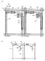
Example 3
Here, a more detailed top surface structure of the pixel portion is shown in FIG. 7A, and a circuit diagram is shown in FIG. 7B. In FIG. 7, the switching
[0096]
Note that although a double gate structure in which two channel formation regions are formed is used in this embodiment, a single gate structure in which one channel formation region is formed or a triple gate structure in which three channel formation regions are formed may be used.
[0097]
The source of the switching
[0098]
The source of the
[0099]
At this time, a storage capacitor (capacitor) is formed in a region indicated by 719. The
[0100]
It should be noted that the configuration of this embodiment can be implemented in combination with any of the configurations of Embodiment 1 and Embodiment 2.
[0101]
Example 4
In this embodiment, a circuit diagram of a pixel portion of a light-emitting device having a structure different from that shown in Embodiment 1 is shown in FIG.
[0102]
First, in FIG. 8A,
[0103]
The drain of the erasing TFT 807 is connected to the gate electrode of the
[0104]
Next, a cross-sectional structure will be described. In FIG. 8B, an n-channel TFT formed by a known method is used as the switching
[0105]
Next, the erasing TFT 807 uses an n-channel TFT formed by a known method. Note that a p-channel TFT formed using a known method may be used. Note that the
[0106]
In this embodiment, the structures of the switching
[0107]
The
[0108]
Note that the structure of the
[0109]
In this embodiment, the
[0110]
The
[0111]
A
[0112]
A transparent conductive film is used as the pixel electrode (anode) 843. Specifically, a conductive film made of a compound of indium oxide and zinc oxide is used. Of course, a conductive film made of a compound of indium oxide and tin oxide may be used.
It is electrically connected to the drain region of the
[0113]
In addition, an
[0114]
There are various types of PPV organic EL materials such as “H. Shenk, H. Becker, O. Gelsen, E. Kluge, W. Kreuder, and H. Spreitzer,“ Polymers for Light Emitting ”. Materials such as those described in “Diodes”, Euro Display, Proceedings, 1999, p. 33-37 ”and Japanese Patent Laid-Open No. 10-92576 may be used.
[0115]
In this embodiment, cyanopolyphenylene vinylene is used for the light emitting layer emitting red light, polyphenylene vinylene is used for the light emitting layer emitting green light, and polyphenylene vinylene or polyalkylphenylene is used for the light emitting layer emitting blue light. The film thickness may be 30 to 150 nm (preferably 40 to 100 nm).
[0116]
However, the above example is an example of an organic EL material that can be used for a light emitting layer for forming an EL layer, and is not necessarily limited to this. In the present invention, an EL layer (a layer composed of materials having different functions such as a hole injection layer, a hole transport layer, a light emitting layer, an electron transport layer, an electron injection layer, a hole blocking layer and a buffer layer) can be freely combined. A layer for causing light emission and carrier movement therefor may be formed.
[0117]
For example, in this embodiment, an example in which a polymer material is used as the light emitting layer is shown, but a low molecular weight organic EL material may be used. It is also possible to use an inorganic material such as silicon carbide for the charge transport layer or the charge injection layer. As these organic EL materials and inorganic materials, known materials can be used.
[0118]
On the
[0119]
When the
[0120]
In this embodiment, a
[0121]
As described above, the light-emitting device of the present invention has a structure as shown in FIG. 8, and includes a switching TFT having a sufficiently low off-current value and a current control TFT that is resistant to hot carrier injection. Therefore, a light emitting device having high reliability and capable of displaying a good image can be obtained. Although only the structure of the pixel portion has been described in this embodiment, the drive circuit has the same configuration as that shown in Embodiment 1.
[0122]
In addition, the structure of a present Example can be implemented in combination with any structure of Example 1- Example 3 freely.
[0123]
Example 5
Next, FIG. 9A shows a circuit diagram of a pixel portion of a light-emitting device in which the present invention is implemented with a structure different from that in Embodiment 4, and FIG. 9B shows a cross-sectional structure of the pixel portion.
The details of the driving method and the like may be referred to Japanese Patent Application No. 2000-127384.
[0124]
First, in FIG. 9A, reference numeral 901 denotes a source signal line connected to the source of the switching
[0125]
The drain of the erasing TFT 907 is connected to the gate electrode of the current control TFT 904 so that the gate voltage of the current control TFT 904 can be forcibly changed. Note that the erasing TFT 907 may be either an n-channel TFT or a p-channel TFT, but preferably has the same structure as the switching
[0126]
In this embodiment, as the current control TFT 904, a first
[0127]
In this embodiment, the first
[0128]
A cross-sectional view of the light-emitting device in this example is shown in FIG. 9B, but the description is omitted because it has almost the same structure as that shown in Example 3, but in the description of FIG. As mentioned above, there are two current control TFTs and they are formed in parallel. This will be described.
[0129]
In FIG. 9B, the current control TFT 904 includes a first
[0130]
The gate electrode 934 (934a, 934b) of the first
[0131]
In this embodiment, the structures of the switching
[0132]
Although only the structure of the pixel portion has been described in this embodiment, the drive circuit has the same configuration as that shown in Embodiment 1.
In addition, the configuration of this embodiment can be implemented by freely combining with any of the configurations of Embodiments 1 to 4.
[0133]
Example 6
In driving the light emitting device of the present invention, analog driving using an analog signal as an image signal can be performed, or digital driving using a digital signal can be performed.
[0134]
When analog driving is performed, an analog signal is sent to the source wiring of the switching TFT, and the analog signal including the gradation information becomes the gate voltage of the current control TFT. Then, the current control TFT controls the current flowing in the EL element, and the light emission intensity of the EL element is controlled to perform gradation display. Note that when analog driving is performed, the current control TFT is preferably operated in a saturation region.
[0135]
On the other hand, in the case of performing digital driving, gradation display called time-division driving is performed unlike analog gradation display. That is, the color gradation is visually changed by adjusting the length of the light emission time. In the case of performing digital driving, the current control TFT is preferably operated in a linear region.
[0136]
Since an EL element has a very high response speed compared to a liquid crystal element, it can be driven at a high speed. Therefore, it can be said that the element is suitable for time-division driving in which gradation display is performed by dividing one frame into a plurality of subframes.
[0137]
As described above, since the present invention is a technique related to an element structure, any driving method may be used.
[0138]
In addition, the structure of a present Example can be implemented in combination with any structure of Example 1- Example 5 freely.
[0139]
Example 7
Since the light-emitting device of the present invention is a self-luminous type, it has excellent visibility in a bright place as compared with a liquid crystal display, and has a wide viewing angle. Therefore, it can be used as a display unit of various electric appliances. For example, in order to appreciate TV broadcasting or the like on a large screen, the light emitting device of the present invention may be used in a display portion of a display device having a diagonal of 30 inches or more (typically 40 inches or more).
[0140]
The display device includes all information display devices such as a personal computer display device, a TV broadcast receiving display device, and an advertisement display device. In addition, the light-emitting device of the present invention can be used for display portions of various electric appliances.
[0141]
Such an electric appliance of the present invention includes a video camera, a digital camera, a goggle type display device (head mounted display), a navigation system, a sound reproduction device (car audio, audio component, etc.), a notebook type personal computer, a game machine, A portable information terminal (mobile computer, mobile phone, portable game machine, electronic book, or the like), an image playback device equipped with a recording medium (specifically, a playback medium such as a digital video disc (DVD)) A device having a display capable of displaying). In particular, a portable information terminal that is often viewed from an oblique direction emphasizes the wide viewing angle, and thus it is desirable to use a light emitting device. Specific examples of these electric appliances are shown in FIGS.
[0142]
FIG. 10A illustrates a display device, which includes a housing 1001, a
[0143]
FIG. 10B shows a video camera, which includes a main body 1011, a display portion 1012, an
[0144]
FIG. 10C shows a part (right side) of the head mounted display, which includes a main body 1021, a
[0145]
FIG. 10D illustrates an image reproducing device (specifically, a DVD reproducing device) provided with a recording medium, which includes a main body 1031, a recording medium (DVD or the like) 1032, an
[0146]
FIG. 10E illustrates a goggle type display device (head mounted display), which includes a main body 1041, a
[0147]
FIG. 10F illustrates a personal computer, which includes a main body 1051, a housing 1052, a display portion 1053, a
[0148]
If the emission brightness of the EL material is increased in the future, the light including the output image information can be enlarged and projected by a lens or the like and used for a front type or rear type projector.
[0149]
In addition, the electric appliances often display information distributed through electronic communication lines such as the Internet or CATV (cable television), and in particular, opportunities to display moving image information are increasing. Since the response speed of the EL material is very high, the light emitting device of the present invention is preferable for displaying moving images.
[0150]
FIG. 11A illustrates a mobile phone, which includes a
[0151]
FIG. 11B shows a sound reproducing device, specifically a car audio, which includes a main body 1111, a
[0152]
FIG. 11C illustrates a digital camera, which includes a main body 1121, a display portion (A) 1122, an eyepiece 1123, operation switches 1124, a display portion (B) 1125, and a battery 1126. The light-emitting device of the present invention can be used in the display portion (A) 1122 and the display portion (B) 1125. Further, when the display portion (B) 1125 is mainly used as an operation panel, power consumption can be suppressed by displaying white characters on a black background.
[0153]
Further, in the portable electric appliance shown in this embodiment, as a method for reducing power consumption, a sensor unit for sensing external brightness is provided, and when used in a dark place, a display unit is provided. For example, there is a method of adding a function such as reducing the brightness of the image.
[0154]
As described above, the application range of the present invention is extremely wide and can be used for electric appliances in various fields. Moreover, you may apply any structure shown in Example 1- Example 6 to the electric appliance of a present Example.
[0155]
【The invention's effect】
By implementing the present invention, TFTs having different structures in the gate electrode and the low concentration impurity region can be manufactured in the driver circuit and the pixel portion of the light emitting device. As a result, it is possible to solve at a time the problems of improving the on-current expected for the TFT of the drive circuit, countermeasures against hot carriers, and reducing the off-current expected of the TFT of the pixel portion. Further, it is possible to solve a problem in the process that has occurred at the time of manufacturing the p-channel TFT in the pixel portion.
[Brief description of the drawings]
FIG. 1 illustrates an embodiment of the present invention.
FIGS. 2A and 2B are diagrams illustrating a manufacturing process of a light-emitting device of the present invention. FIGS.
FIGS. 3A to 3C are diagrams illustrating a manufacturing process of a light-emitting device of the present invention. FIGS.
FIGS. 4A to 4C are diagrams illustrating a manufacturing process of a light-emitting device of the present invention. FIGS.
FIGS. 5A and 5B are diagrams illustrating a manufacturing process of a light-emitting device of the present invention. FIGS.
FIG. 6 shows a sealing structure of a light emitting device of the present invention.
7A and 7B are a top view structure and a circuit diagram of a pixel portion of a light emitting device of the present invention.
8A and 8B are a circuit diagram and a cross-sectional view of a pixel portion of a light emitting device of the present invention.
9A and 9B are a circuit diagram and a cross-sectional view of a pixel portion of a light-emitting device of the present invention.
FIG. 10 is a diagram showing a specific example of an electric appliance using the light-emitting device of the present invention.
FIG. 11 is a diagram showing a specific example of an electric appliance using the light-emitting device of the present invention.
Claims (7)
前記第1の半導体層の上方にゲート絶縁膜を介して第1の導電層と、前記第1の導電層の上方に前記第1の導電層よりもチャネル長方向の幅が狭い第2の導電層とを形成し、
第2の半導体層の上方にゲート絶縁膜を介して第3の導電層と、前記第3の導電層の上方に前記第3の導電層よりもチャネル長方向の幅が狭い第4の導電層とを形成し、
前記第1の導電層および前記第2の導電層をマスクにして、前記ゲート絶縁膜を介して前記第1の半導体層に不純物を添加することにより高濃度不純物領域を形成し、
前記第3の導電層および前記第4の導電層をマスクにして、前記ゲート絶縁膜を介して前記第2の半導体層に不純物を添加することにより高濃度不純物領域を形成し、
前記第2の導電層をマスクにして、前記ゲート絶縁膜および前記第1の導電層を介して前記第1の半導体層に不純物を添加することにより低濃度不純物領域を形成し、
前記第4の導電層をマスクにして、前記ゲート絶縁膜および前記第3の導電層を介して前記第2の半導体層に不純物を添加することにより低濃度不純物領域を形成し、
前記第4の導電層をマスクにして前記第3の導電層をエッチングし、
前記第1の半導体層、前記第1の導電層および前記第2の導電層を有し、
前記第1の半導体層が有する前記低濃度不純物領域が、前記第1の導電層に重なる位置にある第1のTFTを用いて駆動回路が有するnチャネル型TFTを形成し、
前記第2の半導体層、前記第3の導電層および前記第4の導電層を有し、
前記第2の半導体層が有する前記低濃度不純物領域が、前記第3の導電層に重ならない位置にある第2のTFTを用いて画素部が有するnチャネル型TFTを形成することを特徴とする発光装置の作製方法。Forming a first semiconductor layer and a second semiconductor layer above the substrate;
A first conductive layer via a gate insulating film above the first semiconductor layer, and a second conductive having a width in the channel length direction narrower than that of the first conductive layer above the first conductive layer. Forming a layer,
A third conductive layer above the second semiconductor layer via a gate insulating film, and a fourth conductive layer having a width in the channel length direction narrower than the third conductive layer above the third conductive layer And form the
Using the first conductive layer and the second conductive layer as a mask, a high concentration impurity region is formed by adding an impurity to the first semiconductor layer through the gate insulating film,
Using the third conductive layer and the fourth conductive layer as a mask, a high concentration impurity region is formed by adding an impurity to the second semiconductor layer through the gate insulating film,
Using the second conductive layer as a mask, an impurity is added to the first semiconductor layer through the gate insulating film and the first conductive layer to form a low concentration impurity region,
Using the fourth conductive layer as a mask, an impurity is added to the second semiconductor layer through the gate insulating film and the third conductive layer to form a low concentration impurity region,
Etching the third conductive layer using the fourth conductive layer as a mask,
Having the first semiconductor layer, the first conductive layer and the second conductive layer;
Forming an n-channel TFT included in a driver circuit using the first TFT in which the low-concentration impurity region included in the first semiconductor layer overlaps with the first conductive layer;
The second semiconductor layer, the third conductive layer, and the fourth conductive layer;
An n-channel TFT included in a pixel portion is formed using a second TFT in which the low-concentration impurity region included in the second semiconductor layer is located so as not to overlap with the third conductive layer. A method for manufacturing a light-emitting device.
前記第2のTFTは、スイッチング用TFTであることを特徴とする発光装置の作製方法。The method for manufacturing a light-emitting device, wherein the second TFT is a switching TFT.
前記第1の半導体層の上方にゲート絶縁膜を介して第1の導電層と、前記第1の導電層の上方に前記第1の導電層よりもチャネル長方向の幅が狭い第2の導電層とを形成し、
第2の半導体層の上方にゲート絶縁膜を介して第3の導電層と、前記第3の導電層の上方に前記第3の導電層よりもチャネル長方向の幅が狭い第4の導電層とを形成し、
前記第3の半導体層の上方にゲート絶縁膜を介して第5の導電層と、前記第5の導電層の上方に前記第5の導電層よりもチャネル長方向の幅が狭い第6の導電層とを形成し、
前記第1の導電層および前記第2の導電層をマスクにして、前記ゲート絶縁膜を介して前記第1の半導体層にn型の不純物を添加することによりn型の高濃度不純物領域を形成し、
前記第3の導電層および前記第4の導電層をマスクにして、前記ゲート絶縁膜を介して前記第2の半導体層にn型の不純物を添加することによりn型の高濃度不純物領域を形成し、
前記第5の導電層および前記第6の導電層をマスクにして、前記ゲート絶縁膜を介して前記第3の半導体層にn型の不純物を添加することによりn型の高濃度不純物領域を形成し、
前記第2の導電層をマスクにして、前記ゲート絶縁膜および前記第1の導電層を介して前記第1の半導体層にn型の不純物を添加することによりn型の低濃度不純物領域を形成し、
前記第4の導電層をマスクにして、前記ゲート絶縁膜および前記第3の導電層を介して前記第2の半導体層にn型の不純物を添加することによりn型の低濃度不純物領域を形成し、
前記第6の導電層をマスクにして、前記ゲート絶縁膜および前記第5の導電層を介して前記第3の半導体層にn型の不純物を添加することによりn型の低濃度不純物領域を形成し、
前記第4の導電層をマスクにして前記第3の導電層をエッチングし、前記第6の導電層をマスクにして前記第5の導電層をエッチングし、
エッチングした前記第5の導電層および前記第6の導電層をマスクにして、前記ゲート絶縁膜を介して前記第3の半導体層にp型の不純物を添加することによりp型の不純物領域を形成し、
前記第1の半導体層、前記第1の導電層および前記第2の導電層を有し、
前記第1の半導体層が有する前記低濃度不純物領域が、前記第1の導電層に重なる位置にある第1のTFTを用いて駆動回路が有するnチャネル型TFTを形成し、
前記第2の半導体層、前記第3の導電層および前記第4の導電層を有し、
前記第2の半導体層が有する前記低濃度不純物領域が、前記第3の導電層に重ならない位置にある第2のTFTを用いて画素部が有するnチャネル型TFTを形成し、
前記第3の半導体層、前記第5の導電層および前記第6の導電層を有する第3のTFTを用いて前記画素部が有するpチャネル型TFTを形成することを特徴とする発光装置の作製方法。Forming a first semiconductor layer, a second semiconductor layer, and a third semiconductor layer above the substrate;
A first conductive layer via a gate insulating film above the first semiconductor layer, and a second conductive having a width in the channel length direction narrower than that of the first conductive layer above the first conductive layer. Forming a layer,
A third conductive layer above the second semiconductor layer via a gate insulating film, and a fourth conductive layer having a width in the channel length direction narrower than the third conductive layer above the third conductive layer And form the
A fifth conductive layer above the third semiconductor layer with a gate insulating film interposed therebetween, and a sixth conductive layer having a width in the channel length direction smaller than that of the fifth conductive layer above the fifth conductive layer. Forming a layer,
Using the first conductive layer and the second conductive layer as a mask, an n-type impurity region is formed by adding an n-type impurity to the first semiconductor layer through the gate insulating film. And
Using the third conductive layer and the fourth conductive layer as a mask, an n-type impurity region is formed by adding an n-type impurity to the second semiconductor layer through the gate insulating film. And
Using the fifth conductive layer and the sixth conductive layer as a mask, an n-type impurity region is formed by adding an n-type impurity to the third semiconductor layer through the gate insulating film. And
Using the second conductive layer as a mask, an n-type impurity region is formed by adding an n-type impurity to the first semiconductor layer through the gate insulating film and the first conductive layer. And
Using the fourth conductive layer as a mask, an n-type impurity region is formed by adding an n-type impurity to the second semiconductor layer through the gate insulating film and the third conductive layer. And
Using the sixth conductive layer as a mask, an n-type impurity region is formed by adding an n-type impurity to the third semiconductor layer through the gate insulating film and the fifth conductive layer. And
Etching the third conductive layer using the fourth conductive layer as a mask, etching the fifth conductive layer using the sixth conductive layer as a mask,
Using the etched fifth conductive layer and sixth conductive layer as a mask, a p-type impurity region is formed by adding a p-type impurity to the third semiconductor layer through the gate insulating film. And
Having the first semiconductor layer, the first conductive layer and the second conductive layer;
Forming an n-channel TFT included in a driver circuit using the first TFT in which the low-concentration impurity region included in the first semiconductor layer overlaps with the first conductive layer;
The second semiconductor layer, the third conductive layer, and the fourth conductive layer;
Forming an n-channel TFT included in a pixel portion using a second TFT in which the low-concentration impurity region included in the second semiconductor layer is positioned so as not to overlap the third conductive layer;
A p-channel TFT included in the pixel portion is formed using a third TFT including the third semiconductor layer, the fifth conductive layer, and the sixth conductive layer. Method.
前記第2のTFTは、スイッチング用TFTであり、前記第3のTFTは、電流制御用TFTであることを特徴とする発光装置の作製方法。The method for manufacturing a light-emitting device, wherein the second TFT is a switching TFT, and the third TFT is a current control TFT.
前記スイッチング用TFTのソース及びドレインの一方は、前記電流制御用TFTのゲート電極に電気的に接続され、前記電流制御用TFTのソース及びドレインの一方は、発光素子に電気的に接続されることを特徴とする発光装置の作製方法。One of the source and drain of the switching TFT is electrically connected to the gate electrode of the current control TFT, and one of the source and drain of the current control TFT is electrically connected to the light emitting element. A method for manufacturing a light-emitting device.
前記画素部が有するnチャネル型TFTの前記ゲート絶縁膜は、前記画素部が有するnチャネル型TFTの前記低濃度不純物領域の上方でテーパー形状を有していることを特徴とする発光装置の作製方法。 In any one of Claims 1 thru | or 5,
The gate insulating film of the n-channel TFT included in the pixel portion has a tapered shape above the low-concentration impurity region of the n-channel TFT included in the pixel portion. Method.
前記第1の導電層は、テーパー形状を有していることを特徴とする発光装置の作製方法。The method for manufacturing a light-emitting device, wherein the first conductive layer has a tapered shape.
Priority Applications (1)
| Application Number | Priority Date | Filing Date | Title |
|---|---|---|---|
| JP2001223863A JP4772228B2 (en) | 2000-07-31 | 2001-07-25 | Method for manufacturing light emitting device |
Applications Claiming Priority (4)
| Application Number | Priority Date | Filing Date | Title |
|---|---|---|---|
| JP2000232431 | 2000-07-31 | ||
| JP2000232431 | 2000-07-31 | ||
| JP2000-232431 | 2000-07-31 | ||
| JP2001223863A JP4772228B2 (en) | 2000-07-31 | 2001-07-25 | Method for manufacturing light emitting device |
Publications (3)
| Publication Number | Publication Date |
|---|---|
| JP2002141168A JP2002141168A (en) | 2002-05-17 |
| JP2002141168A5 JP2002141168A5 (en) | 2008-09-11 |
| JP4772228B2 true JP4772228B2 (en) | 2011-09-14 |
Family
ID=26597116
Family Applications (1)
| Application Number | Title | Priority Date | Filing Date |
|---|---|---|---|
| JP2001223863A Expired - Fee Related JP4772228B2 (en) | 2000-07-31 | 2001-07-25 | Method for manufacturing light emitting device |
Country Status (1)
| Country | Link |
|---|---|
| JP (1) | JP4772228B2 (en) |
Families Citing this family (4)
| Publication number | Priority date | Publication date | Assignee | Title |
|---|---|---|---|---|
| JP3778176B2 (en) | 2002-05-28 | 2006-05-24 | セイコーエプソン株式会社 | LIGHT EMITTING DEVICE AND ELECTRONIC DEVICE |
| CN102709478B (en) | 2003-03-26 | 2016-08-17 | 株式会社半导体能源研究所 | Light-emitting device |
| JP2009010242A (en) * | 2007-06-29 | 2009-01-15 | Mitsubishi Electric Corp | Display device, and its manufacturing method |
| CN112396745B (en) * | 2019-07-30 | 2023-09-19 | 中移物联网有限公司 | Gate control method and electronic equipment |
Family Cites Families (5)
| Publication number | Priority date | Publication date | Assignee | Title |
|---|---|---|---|---|
| US6462722B1 (en) * | 1997-02-17 | 2002-10-08 | Seiko Epson Corporation | Current-driven light-emitting display apparatus and method of producing the same |
| US5952789A (en) * | 1997-04-14 | 1999-09-14 | Sarnoff Corporation | Active matrix organic light emitting diode (amoled) display pixel structure and data load/illuminate circuit therefor |
| JP3282582B2 (en) * | 1998-04-21 | 2002-05-13 | 日本電気株式会社 | Top gate type thin film transistor and method of manufacturing the same |
| JP3883706B2 (en) * | 1998-07-31 | 2007-02-21 | シャープ株式会社 | Etching method and method of manufacturing thin film transistor matrix substrate |
| JP4008133B2 (en) * | 1998-12-25 | 2007-11-14 | 株式会社半導体エネルギー研究所 | Semiconductor device |
-
2001
- 2001-07-25 JP JP2001223863A patent/JP4772228B2/en not_active Expired - Fee Related
Also Published As
| Publication number | Publication date |
|---|---|
| JP2002141168A (en) | 2002-05-17 |
Similar Documents
| Publication | Publication Date | Title |
|---|---|---|
| JP6345837B2 (en) | EL display device | |
| US7145177B2 (en) | Light emitting device | |
| JP5941573B2 (en) | Display device | |
| JP4906022B2 (en) | Active matrix EL display device and electronic device | |
| US7265390B2 (en) | Light emitting device | |
| US8017944B2 (en) | Electronic device with light emission for a display | |
| JP4849739B2 (en) | Display panel manufacturing method | |
| JP2002083689A (en) | Luminescence device | |
| JP2000216399A (en) | Semiconductor device and its manufacture | |
| JP2000340801A (en) | Semiconductor device and its manufacture | |
| JP4850326B2 (en) | Method for manufacturing semiconductor device | |
| JP4772228B2 (en) | Method for manufacturing light emitting device |
Legal Events
| Date | Code | Title | Description |
|---|---|---|---|
| A521 | Request for written amendment filed |
Free format text: JAPANESE INTERMEDIATE CODE: A523 Effective date: 20080724 |
|
| A621 | Written request for application examination |
Free format text: JAPANESE INTERMEDIATE CODE: A621 Effective date: 20080724 |
|
| A977 | Report on retrieval |
Free format text: JAPANESE INTERMEDIATE CODE: A971007 Effective date: 20100907 |
|
| A131 | Notification of reasons for refusal |
Free format text: JAPANESE INTERMEDIATE CODE: A131 Effective date: 20101102 |
|
| RD02 | Notification of acceptance of power of attorney |
Free format text: JAPANESE INTERMEDIATE CODE: A7422 Effective date: 20101116 |
|
| A521 | Request for written amendment filed |
Free format text: JAPANESE INTERMEDIATE CODE: A523 Effective date: 20101203 |
|
| TRDD | Decision of grant or rejection written | ||
| A01 | Written decision to grant a patent or to grant a registration (utility model) |
Free format text: JAPANESE INTERMEDIATE CODE: A01 Effective date: 20110621 |
|
| A01 | Written decision to grant a patent or to grant a registration (utility model) |
Free format text: JAPANESE INTERMEDIATE CODE: A01 |
|
| A61 | First payment of annual fees (during grant procedure) |
Free format text: JAPANESE INTERMEDIATE CODE: A61 Effective date: 20110622 |
|
| FPAY | Renewal fee payment (event date is renewal date of database) |
Free format text: PAYMENT UNTIL: 20140701 Year of fee payment: 3 |
|
| R150 | Certificate of patent or registration of utility model |
Ref document number: 4772228 Country of ref document: JP Free format text: JAPANESE INTERMEDIATE CODE: R150 Free format text: JAPANESE INTERMEDIATE CODE: R150 |
|
| FPAY | Renewal fee payment (event date is renewal date of database) |
Free format text: PAYMENT UNTIL: 20140701 Year of fee payment: 3 |
|
| R250 | Receipt of annual fees |
Free format text: JAPANESE INTERMEDIATE CODE: R250 |
|
| R250 | Receipt of annual fees |
Free format text: JAPANESE INTERMEDIATE CODE: R250 |
|
| R250 | Receipt of annual fees |
Free format text: JAPANESE INTERMEDIATE CODE: R250 |
|
| R250 | Receipt of annual fees |
Free format text: JAPANESE INTERMEDIATE CODE: R250 |
|
| R250 | Receipt of annual fees |
Free format text: JAPANESE INTERMEDIATE CODE: R250 |
|
| R250 | Receipt of annual fees |
Free format text: JAPANESE INTERMEDIATE CODE: R250 |
|
| R250 | Receipt of annual fees |
Free format text: JAPANESE INTERMEDIATE CODE: R250 |
|
| LAPS | Cancellation because of no payment of annual fees |