JP4765415B2 - Light emitting diode and manufacturing method thereof - Google Patents
Light emitting diode and manufacturing method thereof Download PDFInfo
- Publication number
- JP4765415B2 JP4765415B2 JP2005162628A JP2005162628A JP4765415B2 JP 4765415 B2 JP4765415 B2 JP 4765415B2 JP 2005162628 A JP2005162628 A JP 2005162628A JP 2005162628 A JP2005162628 A JP 2005162628A JP 4765415 B2 JP4765415 B2 JP 4765415B2
- Authority
- JP
- Japan
- Prior art keywords
- emitting diode
- light emitting
- light
- holes
- region
- Prior art date
- Legal status (The legal status is an assumption and is not a legal conclusion. Google has not performed a legal analysis and makes no representation as to the accuracy of the status listed.)
- Expired - Fee Related
Links
Images

Landscapes
- Led Devices (AREA)
Description
本発明は、発光ダイオード及びその製造方法に関する。特に光取出し効率の良好な発光ダイオード(LED)の構造、及びそのような構造を有する発光ダイオードの製造方法に関するものである。 The present invention relates to a light emitting diode and a method for manufacturing the same. In particular, the present invention relates to a structure of a light emitting diode (LED) with good light extraction efficiency and a method for manufacturing the light emitting diode having such a structure.
発光ダイオードは、基板上に発光層を含む複数の半導体層が結晶成長により積層して成る。発光層で発生した光を素子表面の一部から射出する形式の発光ダイオードにおける最も重要な性能指数としては、効率が挙げられる。発光ダイオードにおいては、可能な限り少ない電流で高い光出力が得られること、すなわち、高効率であることが望まれる。 A light emitting diode is formed by laminating a plurality of semiconductor layers including a light emitting layer on a substrate by crystal growth. The most important figure of merit in a light emitting diode that emits light generated in the light emitting layer from a part of the element surface is efficiency. In a light emitting diode, it is desired that high light output can be obtained with as little current as possible, that is, high efficiency.
一般に効率は、内部量子効率と光取出し効率で決定される。ここで、内部量子効率とは、素子内部において電気を光に変換する効率であり、注入電流が発光層内で光子に変換される効率である。また、光取出し効率とは、発光層で発生した光が素子の外部に取り出される効率である。光取出し効率×内部量子効率を、外部量子効率という。 In general, efficiency is determined by internal quantum efficiency and light extraction efficiency. Here, the internal quantum efficiency is the efficiency of converting electricity into light inside the device, and is the efficiency of converting the injected current into photons in the light emitting layer. The light extraction efficiency is the efficiency with which light generated in the light emitting layer is extracted outside the device. The light extraction efficiency × internal quantum efficiency is called external quantum efficiency.
内部量子効率については、一般的に市販されている発光ダイオードのほぼ全てにおいて50%以上の値が既に得られており、中にはほぼ100%の内部量子効率が達成されている例もある。 As for the internal quantum efficiency, a value of 50% or more has already been obtained in almost all of the light-emitting diodes that are generally marketed, and there are examples in which an internal quantum efficiency of almost 100% has been achieved.
一方、光取出し効率は、光取出し面における発光素子内部と外部の屈折率の比やその面性状に依存することが知られている。発光ダイオードに一般的に用いられる化合物半導体の屈折率(n)は、n=2.2〜3.8(例えば、GaAs(ガリウム−砒素)ではn=3.5)であって、空気(真空)の屈折率の値(n=1)に比較して極めて大きい。 On the other hand, it is known that the light extraction efficiency depends on the ratio of the refractive index inside and outside the light emitting element on the light extraction surface and the surface properties. The refractive index (n) of a compound semiconductor generally used in a light emitting diode is n = 2.2 to 3.8 (for example, n = 3.5 in GaAs (gallium-arsenide)), and air (vacuum) ) Of the refractive index (n = 1).
発光素子から外部に射出されうる光は、スネルの法則に従い、発光素子内部から表面への光の入射角が臨界角(θc)以下のものに制限される。発光ダイオードに一般的に用いられる化合物半導体の屈折率が空気(真空)の屈折率に比較して極めて大きいため、発光層で発生した光の大部分を素子外部に取り出せない状況となる。例えば、屈折率の値が3.5であるGaAsの場合、臨界角は、θc=16.6度であり、全発光の約2%しか素子の外部に取り出せないことになる。 The light that can be emitted from the light emitting element to the outside is limited to light having an incident angle from the inside of the light emitting element to the surface that is equal to or smaller than the critical angle (θ c ) in accordance with Snell's law. Since the refractive index of a compound semiconductor generally used for a light emitting diode is very large compared to the refractive index of air (vacuum), most of the light generated in the light emitting layer cannot be taken out of the device. For example, in the case of GaAs having a refractive index value of 3.5, the critical angle is θ c = 16.6 degrees, and only about 2% of the total light emission can be extracted outside the device.
光取出し効率向上のためには、例えば、エッチング処理を施して、光取出し面を適度に荒らすことによりその光取出し面に臨界角以上の角度で入射する割合を減らして、光取出し効率を向上することが提案されている(例えば、特許文献1参照)。
特許文献1に示された発光ダイオードは、例えば、かまぼこ状にしたレジストパターンによりシリンドリカル・レンズ状やロッドレンズ状の凸凹にエッチング処理した後のp型GaN層の一部(パッド電極が形成される部分)に電流阻止層としての絶縁膜を形成し、そのp型GaN層と絶縁膜の上にp側パッド電極を積層し、光はp側パッド電極以外の領域から透明導電膜を介して複数の線状ビームとして放出される。 For example, the light emitting diode disclosed in Patent Document 1 is a part of a p-type GaN layer (pad electrode is formed after etching into a cylindrical lens shape or rod lens shape unevenness by a resist pattern having a semi-cylindrical shape. Part) is formed with an insulating film as a current blocking layer, a p-side pad electrode is laminated on the p-type GaN layer and the insulating film, and light is transmitted from a region other than the p-side pad electrode through a transparent conductive film. Is emitted as a linear beam.
特許文献1に示されているように、光取出し効率を考える上では、表面の性状と並んで重要な要素に電極配置がある。すなわち、発光ダイオード表面に設置される電極の少なくとも一部には、電源から電極へ配線を施すためにある程度の機械的強度を持たせる必要があり、光が透過できない程度に電極膜厚を厚くしているパッド電極と呼ばれる領域が存在する。パッド電極は、素子外部への光取出しを阻害するため、高い光取出し効率を得るためにはパッド電極直下以外の発光層に効率よく給電する工夫(電流分散)が必要となる。代表的な例としては、下記の(1)及び(2)の方法が挙げられる。 As shown in Patent Document 1, in consideration of light extraction efficiency, electrode arrangement is an important element along with surface properties. In other words, at least a part of the electrodes installed on the surface of the light emitting diode must have a certain degree of mechanical strength for wiring from the power source to the electrodes, and the electrode film thickness is increased to such an extent that light cannot be transmitted. There is a region called a pad electrode. Since the pad electrode hinders light extraction to the outside of the element, in order to obtain high light extraction efficiency, a device (current distribution) for efficiently supplying power to the light emitting layer other than immediately below the pad electrode is required. Typical examples include the following methods (1) and (2).
(1)パッド電極から供給されたキャリアが発光層に到達するまでに十分広がるように、電極形成表面と発光層の間の距離を十分大きく取る(>10μm)。 (1) The distance between the electrode formation surface and the light emitting layer is made sufficiently large (> 10 μm) so that the carriers supplied from the pad electrode spread sufficiently until they reach the light emitting layer.
(2)発光ダイオード表面のほぼ全体に渡り、薄い透明導電膜を設置し、その上の一部にパッド電極を設置する。 (2) A thin transparent conductive film is provided over almost the entire surface of the light emitting diode, and a pad electrode is provided on a part of the thin transparent conductive film.
上記(1)の方法は、発光層等と同時に結晶成長で実施できる簡便な方法であるが、(A)成長膜厚が増大し、製造コストが上がる、(B)発光層の表面側に厚膜があると、そこでの光吸収により効率が低下する場合がある、といったデメリットがある。 The method (1) is a simple method that can be carried out by crystal growth simultaneously with the light emitting layer, etc., but (A) the growth film thickness increases and the manufacturing cost increases, and (B) the thickness increases on the surface side of the light emitting layer. If there is a film, there is a demerit that efficiency may decrease due to light absorption there.
上記(A)及び(B)のデメリットは、上記(2)の方法の透明導電膜を使用することにより回避可能であり、素子制作上の困難が伴わなければ、コスト面及びLED効率の面から好ましいと言える。 The disadvantages (A) and (B) can be avoided by using the transparent conductive film of the method (2), and from the viewpoint of cost and LED efficiency, if there are no difficulties in device production. It can be said that it is preferable.
しかし、特許文献1の発光ダイオードによると、透明導電膜の厚さは、一般的に5〜100nmと非常に薄く、表面にエッチング処理を施して形成した凸凹の段差(>100nm)が存在するため、透明導電膜を光取出し面全体に連続して形成することが困難である。 However, according to the light emitting diode of Patent Document 1, the thickness of the transparent conductive film is generally very thin, 5 to 100 nm, and there are uneven steps (> 100 nm) formed by etching the surface. It is difficult to continuously form a transparent conductive film over the entire light extraction surface.
特許文献1に示されるように、シリンドリカル・レンズ状やロッドレンズ状の凸凹を有する発光ダイオードによると、光放出表面に形成された凸凹面が、例えば100nmの深さを有し、凸面上に透明導電膜材料を蒸着していたため、透明導電膜を発光面全体に連続して形成することが困難であった。 As shown in Patent Document 1, according to a light emitting diode having cylindrical lens-like or rod lens-like irregularities, the irregular surface formed on the light emitting surface has a depth of, for example, 100 nm and is transparent on the convex surface. Since the conductive film material was deposited, it was difficult to continuously form the transparent conductive film over the entire light emitting surface.
即ち、本発明が解決しようとする課題は、表面をエッチングにより荒らした領域を有する発光ダイオードにおいて、当該エッチング領域に薄膜の透明導電膜を有効な形で、すなわち発光面全体に連続して形成することが困難な点である。 That is, the problem to be solved by the present invention is that in a light-emitting diode having a region whose surface is roughened by etching, a thin transparent conductive film is effectively formed in the etched region, that is, continuously formed on the entire light-emitting surface. This is a difficult point.
したがって、本発明の目的は、上記した課題を解決し、表面の少なくとも一部にエッチングにより荒らした領域(エッチング領域)を有する発光ダイオードにおいて、当該エッチング領域に薄膜の透明導電膜を有効な形で形成でき、LED効率を大幅に向上することが可能である発光ダイオード及びその製造方法を提供することにある。より詳細には、表面の少なくとも一部にエッチングにより荒らした領域を有する発光ダイオードにおいて、当該エッチング領域に薄膜の透明導電膜を有効な形で、すなわち発光面全体に連続して形成するための、エッチング形状、ダイオード構造、及びそれらの製造方法を提供することにある。 Accordingly, an object of the present invention is to solve the above-described problems, and in a light-emitting diode having a region (etching region) roughened by etching on at least a part of the surface, a thin transparent conductive film is effectively formed in the etching region. It is an object of the present invention to provide a light emitting diode that can be formed and can greatly improve LED efficiency, and a method of manufacturing the same. More specifically, in a light emitting diode having a region roughened by etching on at least a part of the surface, a thin transparent conductive film is effectively formed in the etched region, that is, continuously formed on the entire light emitting surface. An object of the present invention is to provide an etching shape, a diode structure, and a manufacturing method thereof.
本発明者らは上記課題を解決するため鋭意研究を行った結果、エッチング領域に適切な密度及び面積比率でエッチングによる穴を分布させ、エッチング領域における穴以外の部分をエッチング前の初期表面と概ね平行な面として残留せしめることにより、光取出し効率を向上しつつ、少なくともエッチングに領域における穴以外の部分には、透明導電膜を導通可能な状態で形成可能であり、透明導電膜による電流分散と表面エッチングによる光取出し効率の向上が両立可能であることを見出した。 As a result of diligent research to solve the above problems, the present inventors have distributed etching holes at an appropriate density and area ratio in the etching region, and the portions other than the holes in the etching region are roughly the same as the initial surface before etching. By allowing the transparent conductive film to remain as parallel surfaces, the transparent conductive film can be formed in a conductive state at least in a portion other than the hole in the etching region while improving the light extraction efficiency. It was found that light extraction efficiency can be improved by surface etching.
本発明に係る発光ダイオードは、基板上に、前記基板側からn型半導体層、多重量子井戸層、及びp型半導体層を順に形成することにより作製された半導体領域を有する発光ダイオードにおいて、前記半導体領域の前記基板と反対側の表面にエッチングにより不連続でランダムに独立した複数の穴を形成することにより作製された高効率光取出し領域、前記高効率光取出し領域の前記複数の穴の外部の平坦領域にのみ透明導電膜からなる透明電極を連続的に断線することなく形成することにより作製された透明電極形成領域を有し、前記高効率光取出し領域における前記複数の穴の面積割合が40%以上70%以下、かつ前記高効率光取出し領域における前記複数の穴の密度が1×10⁶個/cm2以上1×1010個/cm2以下であることを特徴とする。
The light-emitting diode according to the present invention is a light-emitting diode having a semiconductor region formed by sequentially forming an n-type semiconductor layer , a multiple quantum well layer, and a p-type semiconductor layer from the substrate side on the substrate. A high-efficiency light extraction region produced by forming a plurality of discontinuous and randomly independent holes by etching on the surface of the region opposite to the substrate; outside the plurality of holes of the high-efficiency light extraction region It has a transparent electrode forming region produced by continuously forming a transparent electrode made of a transparent conductive film only in a flat region without disconnection, and the area ratio of the plurality of holes in the high-efficiency light extraction region is 40 % To 70% and the density of the plurality of holes in the high-efficiency light extraction region is 1 × 10 6 holes / cm 2 to 1 × 10 10 holes / cm 2. It shall be the butterfly.
本発明に係る発光ダイオードは、前記透明電極上にp型電極を設け、前記p型電極が設けられる直下の領域の前記p型半導体層側にSiO2膜を設けてもよい。
Light emitting diode according to the present invention, the p-type electrode provided in front Symbol transparent electrode, may be provided SiO 2 film on the p-type semiconductor layer side of the region immediately below said p-type electrode is provided.
本発明に係る発光ダイオードは、前記透明電極形成領域が、前記高効率光取出し領域の80%以上を覆うように形成されていることが好ましい。なぜならば、高効率光取出し領域上の透明電極形成領域が覆う割合が低いと、十分な電流分散が得られないため、LEDの発光効率を十分に向上できないからである。なお、前記割合は、理想的には100%にするのが好ましいが、リソグラフィーの位置合わせ精度の問題から、100%にはできないのが現実である。 In the light emitting diode according to the present invention, it is preferable that the transparent electrode forming region is formed so as to cover 80% or more of the high efficiency light extraction region. This is because if the ratio of the transparent electrode formation region on the high-efficiency light extraction region is low, sufficient current distribution cannot be obtained, and the light emission efficiency of the LED cannot be sufficiently improved. The ratio is ideally preferably 100%, but in reality, it cannot be 100% due to the problem of lithography alignment accuracy.
本発明に係る発光ダイオードは、前記複数の穴の各開口部が、概円形で開口部の直径が50nm以上1000nm以下、又は多角形で開口部の外接円の直径が50nm以上1000nm以下であることが好ましい。 In the light-emitting diode according to the present invention, each opening of the plurality of holes is substantially circular and the diameter of the opening is 50 nm or more and 1000 nm or less, or a polygon and the diameter of the circumscribed circle of the opening is 50 nm or more and 1000 nm or less. Is preferred.
本発明に係る発光ダイオードは、前記複数の穴が、概円形あるいは多角形が独立した穴と、不定形の穴からなることが好ましい。 In the light emitting diode according to the present invention, it is preferable that the plurality of holes include a substantially circular or polygonal independent hole and an indeterminate hole.
本発明に係る発光ダイオードは、前記複数の穴の深さが、前記p型半導体層の厚さ未満であることが好ましい。 In the light emitting diode according to the present invention, it is preferable that the depth of the plurality of holes is less than the thickness of the p-type semiconductor layer.
本発明に係る発光ダイオードは、前記半導体領域を構成する半導体が、III−V族化合物半導体あるいは窒化物半導体であることが好ましい。以下に述べる実施例では、窒化物半導体を用いているが、本発明はこれに限定されるものではなく、GaAs、AlGaAs、InGaAs、InGaAsP等の窒素を含まないIII−V族化合物半導体からなる発光ダイオードに対しても適用可能であり、且つ、窒化物半導体を用いた場合と同様な発光効率の向上効果を得ることができる。 In the light emitting diode according to the present invention, the semiconductor constituting the semiconductor region is preferably a III-V compound semiconductor or a nitride semiconductor. In the embodiments described below, a nitride semiconductor is used. However, the present invention is not limited to this, and light emission made of a group III-V compound semiconductor containing no nitrogen such as GaAs, AlGaAs, InGaAs, InGaAsP or the like. The present invention can also be applied to a diode, and the same light emission efficiency improvement effect as that obtained when a nitride semiconductor is used can be obtained.
前記窒化物半導体としては、InAlGaNを用いるのが好ましい。 InAlGaN is preferably used as the nitride semiconductor.
前記半導体の結晶成長は気相成長装置内で行うのが好ましく、例えば、有機金属気相成長(MOVPE)装置又はハイドライド気相成長(HVPE)装置内で行うのが好ましい。 Crystal growth of the semiconductor is preferably performed in a vapor phase growth apparatus, for example, in a metal organic vapor phase growth (MOVPE) apparatus or a hydride vapor phase growth (HVPE) apparatus.
本発明に係る発光ダイオードは、前記半導体領域が、サファイア、SiC、Si、GaN、AlN、ZnO、ZrB2のいずれかからなる基板上に形成されていることが好ましい。以下に述べる実施例では、サファイア基板が用いられているが、本発明はこれに限定されるものではなく、SiC、Si、GaN、AlN、ZnO、ZrB2等からなる基板であっても適用可能である。 Light emitting diode according to the present invention, the semiconductor region, sapphire, SiC, Si, GaN, AlN, ZnO, that are formed on a substrate made of any of the ZrB 2 preferred. In the embodiments described below, a sapphire substrate is used, but the present invention is not limited to this, and can be applied to a substrate made of SiC, Si, GaN, AlN, ZnO, ZrB 2 or the like. It is.
本発明に係る発光ダイオードは、透明導電膜が、Ni、Pt、Au、ITO、ZnOのうち少なくとも一つを含むことが好ましい。 In the light emitting diode according to the present invention, the transparent conductive film preferably contains at least one of Ni, Pt, Au, ITO, and ZnO.
本発明に係る発光ダイオードの製造方法は、少なくともp型半導体層及びn型半導体層からなる半導体領域を形成する段階、前記半導体領域の表面に複数の穴を形成することにより高効率光取出し領域を作製する段階、前記高効率光取出し領域の平坦領域に透明導電膜からなる透明電極を形成することにより透明電極形成領域を作製する段階を含むことが好ましく、前記透明電極は、斜め蒸着法により作製されることが好ましい。
The method for manufacturing a light emitting diode according to the present invention includes a step of forming a semiconductor region including at least a p-type semiconductor layer and an n-type semiconductor layer, and forming a plurality of holes in the surface of the semiconductor region to form a highly efficient light extraction region. step of making, rather is preferable that it comprises the step of preparing a transparent electrode forming region by forming a transparent electrode made of a transparent conductive film on the flat region of the high-efficiency light extraction region, the transparent electrode, an oblique vapor deposition method It is preferable to be manufactured by.
本発明に係る発光ダイオードの製造方法は、前記複数の穴を形成する方法として、酸溶液又はアルカリ溶液によるウェットエッチングを用いることが好ましい。 In the method of manufacturing a light emitting diode according to the present invention, it is preferable to use wet etching with an acid solution or an alkali solution as a method of forming the plurality of holes.
本発明に係る発光ダイオードの製造方法は、前記複数の穴を形成する方法として、酸溶液又はアルカリ溶液を用いた電気化学的エッチングを用いることが好ましい。 In the method for manufacturing a light emitting diode according to the present invention, it is preferable to use electrochemical etching using an acid solution or an alkali solution as a method of forming the plurality of holes.
本発明に係る発光ダイオードの製造方法は、前記電気化学的エッチングとして、パルスエッチングを用いることが好ましい。 In the method for manufacturing a light emitting diode according to the present invention, it is preferable to use pulse etching as the electrochemical etching.
本発明に係る発光ダイオードの製造方法は、前記高効率光取出し領域を作製する段階は、前記半導体領域の表面に酸溶液又はアルカリ溶液を用いた電気化学的エッチングにより多孔質構造を形成する段階、酸溶液又はアルカリ溶液を用いたウェットエッチングにより多孔質構造を除去する段階から成ることが好ましい。 In the method of manufacturing a light emitting diode according to the present invention, the step of producing the high-efficiency light extraction region includes a step of forming a porous structure on the surface of the semiconductor region by electrochemical etching using an acid solution or an alkali solution, Preferably, the method comprises a step of removing the porous structure by wet etching using an acid solution or an alkali solution.
本発明に係る発光ダイオードの製造方法は、前記前記酸溶液又はアルカリ溶液として、H2SO4、H3PO4、HCl、KOH、NaOHのうち少なくとも一つを含む溶液を用いることが好ましい。 In the light emitting diode manufacturing method according to the present invention, it is preferable to use a solution containing at least one of H 2 SO 4 , H 3 PO 4 , HCl, KOH, and NaOH as the acid solution or the alkali solution.
本発明に係る発光ダイオードの製造方法は、前記複数の穴を形成する方法として、ドライエッチングを用いることが好ましい。 In the method for manufacturing a light emitting diode according to the present invention, dry etching is preferably used as the method for forming the plurality of holes.
本発明に係る発光ダイオードの製造方法は、前記ドライエッチングにおいて、エッチングガスとして、HCl、Cl2、SF6、BCl3、CH4のうち少なくとも一つを含むことが好ましい。 The light emitting diode manufacturing method according to the present invention preferably includes at least one of HCl, Cl 2 , SF 6 , BCl 3 , and CH 4 as an etching gas in the dry etching.
本発明に係る発光ダイオードの製造方法は、透明導電膜が、Ni、Pt、Au、ITO、ZnOのうち少なくとも一つを含むことが好ましい。 In the method for manufacturing a light emitting diode according to the present invention, the transparent conductive film preferably contains at least one of Ni, Pt, Au, ITO, and ZnO.
本発明による発光ダイオードは、上述したとおりであるので、表面の少なくとも一部にエッチングにより荒らした領域(エッチング領域)を有する発光ダイオードにおいて、当該エッチング領域に薄膜の透明導電膜を有効な形で形成でき、LED効率を大幅に向上することが可能である。本発明の発光ダイオードの製造方法では、エッチングにより不連続でランダムに独立した穴を形成するため、薄膜の透明導電膜を断線することなく連続して形成でき、LED効率を大幅に向上することが可能である。 Since the light-emitting diode according to the present invention is as described above, in a light-emitting diode having a region (etched region) roughened by etching on at least a part of the surface, a thin transparent conductive film is effectively formed in the etched region. It is possible to greatly improve the LED efficiency. In the method for producing a light emitting diode of the present invention, discontinuous and randomly independent holes are formed by etching, so that a thin transparent conductive film can be continuously formed without disconnection, and the LED efficiency can be greatly improved. Is possible.
また、本発明の発光ダイオードの製造方法では、電流分散の面からも光取出し効率を高めるために発光ダイオード表面のほぼ全体に渡って薄い透明導電膜を設置し、その上の一部にパッド電極を設置するという方法とエッチング処理を表面に施し光取出し面を適度に荒らすという方法を併用するうえでの素子制作上の困難を解消でき、したがって、コスト面及びLED効率の面で有利である。 Further, in the light emitting diode manufacturing method of the present invention, a thin transparent conductive film is provided over almost the entire surface of the light emitting diode in order to increase the light extraction efficiency from the viewpoint of current dispersion, and a pad electrode is formed on a part of the thin transparent conductive film. It is possible to eliminate the difficulty in device fabrication when using the method of installing the substrate and the method of performing the etching treatment on the surface and appropriately roughening the light extraction surface, and this is advantageous in terms of cost and LED efficiency.
本発明の実施形態について、以下に図を用いて詳細に述べるが、本発明はそれらに限定されるものではない。 Embodiments of the present invention will be described in detail below with reference to the drawings, but the present invention is not limited thereto.
<発光ダイオードの構造>
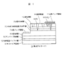
図1は、本発明の発光ダイオードの実施例1である発光ダイオード(LED)構造の断面模式図である。図1に示した本発明の実施例1の発光ダイオード13は、サファイア基板6上に、GaN低温バッファ層12(厚さ22nm)、アンドープGaN層5(厚さ2μm)、n型GaN層4(厚さ4μm)、InGaN/GaN多重量子井戸層3、p型AlGaN層2(厚さ35nm)、p型GaN層1(厚さ200nm)の順に成長させてある。エッチングにより穴8が形成された発光ダイオード(LED)ウエハにn側パッド電極7、SiO2膜10、透明電極9、p側パッド電極11が形成されている。
<Structure of light emitting diode>
FIG. 1 is a schematic cross-sectional view of a light-emitting diode (LED) structure that is Embodiment 1 of the light-emitting diode of the present invention. The light-emitting diode 13 according to the first embodiment of the present invention shown in FIG. 1 includes a GaN low-temperature buffer layer 12 (thickness 22 nm), an undoped GaN layer 5 (thickness 2 μm), an n-type GaN layer 4 ( The InGaN / GaN multiple
エッチングにより形成された穴の深さによっては、発光層(ここでは、InGaN/GaN多重量子井戸層3)およびn型半導体層まで貫通する穴となっているため、p側パッド電極と発光層およびn型半導体層の間の直接の導通を防止する目的で、p側パッド電極の直下にはSiO2膜を形成した。また、同様に透明導電膜と発光層およびn型半導体層の間の直接の導通を防止する目的で透明導電膜の蒸着は、蒸着材料のウエハへの入射方向とウエハ表面が10度以上15度以下の角度を成すように設置する斜め蒸着法により行った。かかる配置を採用することにより、穴の内部への蒸着を最小限に留め、穴の外部の平坦部分にのみ蒸着することが可能である。 Depending on the depth of the hole formed by etching, the hole penetrates to the light emitting layer (here, the InGaN / GaN multiple quantum well layer 3) and the n-type semiconductor layer. In order to prevent direct conduction between the n-type semiconductor layers, an SiO 2 film was formed immediately below the p-side pad electrode. Similarly, for the purpose of preventing direct conduction between the transparent conductive film and the light emitting layer and the n-type semiconductor layer, the transparent conductive film is vapor-deposited with the incident direction of the vapor deposition material on the wafer and the wafer surface being 10 degrees or more and 15 degrees. It was carried out by the oblique vapor deposition method installed so as to form the following angles. By adopting such an arrangement, it is possible to minimize vapor deposition inside the hole and to deposit only on a flat portion outside the hole.
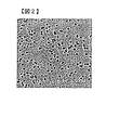
図2は、エッチング後のウエハ表面状態の一例である。図2は、ウエハ表面を電子顕微鏡で拡大して撮影したものである。 FIG. 2 shows an example of the wafer surface state after etching. FIG. 2 is an enlarged image of the wafer surface taken with an electron microscope.
図2に見られるように、本エッチングにより形成された表面形態は、典型的には多数の穴とそれ以外の平坦部分からなっている。エッチング条件により、穴の密度は1×10⁶個/cm2以上1×1010個/cm2以下の範囲で変化した。また、穴の開口部の形状は、円形、六角形、12角形等を主体としているが、これらの融合した不定形の穴も存在した。個々の独立した穴の大きさは、開口部が円形の場合はその直径、多角形の場合にはその外接円の直径で表すと50nm以上1000nm以下の範囲であった。また、穴の深さはエッチング条件により異なるが50nm以上1000nm以下の範囲であった。 As seen in FIG. 2, the surface form formed by this etching typically consists of a number of holes and other flat portions. Depending on the etching conditions, the hole density varied in the range of 1 × 10 6 holes / cm 2 to 1 × 10 10 holes / cm 2 . Moreover, the shape of the opening of the hole is mainly circular, hexagonal, dodecagonal, etc., but there is also an indeterminate hole fused with these. The size of each individual hole was in the range of 50 nm to 1000 nm in terms of the diameter when the opening was circular, and the diameter of the circumscribed circle when the opening was a polygon. The depth of the hole was in the range of 50 nm to 1000 nm, although it varied depending on the etching conditions.
<作用効果>
図3は、本発明の発光ダイオードの実施例1の特性図である。図3は、横軸が穴の開口部が表面に占める割合、縦軸が各ウエハから製作した発光ダイオードの20mA通電時の光出力である。図3に示したように、エッチングを施さない従来構造の発光ダイオードにおける光出力が7mWであったのに対して、エッチングにより表面に穴を形成した場合、穴の開口部が表面に占める割合が10%以上80%以下の場合に光出力が9.2mW以上28mW以下と大幅に向上した。蒸着された透明導電膜は断線することなく連続している。
<Effect>
FIG. 3 is a characteristic diagram of Example 1 of the light-emitting diode according to the present invention. In FIG. 3, the horizontal axis represents the ratio of the opening of the hole to the surface, and the vertical axis represents the light output of the light emitting diode manufactured from each wafer when 20 mA is energized. As shown in FIG. 3, the light output of a conventional light emitting diode without etching is 7 mW, whereas when holes are formed in the surface by etching, the ratio of the hole openings to the surface is In the case of 10% or more and 80% or less, the light output was greatly improved to 9.2 mW or more and 28 mW or less. The deposited transparent conductive film is continuous without disconnection.
穴の開口部が表面に占める割合が80%よりも大きい場合には、透明導電膜が面内の各所で断線し発光面積が減少したため、光出力は逆に大幅に減少した。 When the ratio of the hole openings to the surface was greater than 80%, the light output decreased significantly because the transparent conductive film was disconnected at various locations within the surface and the light emission area decreased.
したがって、本発明の発光ダイオードによれば、表面の少なくとも一部にエッチングにより荒らした領域を有する発光ダイオードにおいて、当該エッチング領域に薄膜の透明導電膜を有効な形で形成でき、LED効率を大幅に向上することが可能である。 Therefore, according to the light emitting diode of the present invention, in a light emitting diode having a region roughened by etching on at least a part of the surface, a thin transparent conductive film can be effectively formed in the etched region, and the LED efficiency is greatly improved. It is possible to improve.
<発光ダイオードの製造方法>
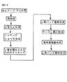
図4は、本発明の発光ダイオードの製造方法の実施例1のフロー図である。図4では、p型GaN層成長以降のフローを示している。
<Method for manufacturing light-emitting diode>
FIG. 4 is a flowchart of Example 1 of the method for manufacturing a light-emitting diode according to the present invention. FIG. 4 shows a flow after the growth of the p-type GaN layer.
まず、2インチ径のC面サファイア基板上にMOVPE法により青色で発光する発光ダイオード(LED)構造を成長した。 First, a light emitting diode (LED) structure that emits blue light was grown on a 2-inch diameter C-plane sapphire substrate by the MOVPE method.
具体的には、サファイア基板をMOVPE装置に導入した後に、760Torrの水素/素混合ガス雰囲気中(総流量=150slm、窒素/水素=2)、1135℃で10分間加熱することにより基板表面の酸化物等を除去した(熱清浄化)。その後、基板温度を515℃に下げると共に、キャリアガス流量を140slm、キャリアガス中の窒素/水素の体積比を1.5として、窒素原料であるアンモニア(NH3)ガスを10slmの流量で成長装置に導入した。更に、Gaの原料としてトリメチルガリウム(TMG)を成長装置に導入し、基板上にGaN低温バッファ層を1.6μm/時の成長速度で22nm成長した。 Specifically, after the sapphire substrate is introduced into the MOVPE apparatus, the substrate surface is oxidized by heating at 1135 ° C. for 10 minutes in a hydrogen / element mixed gas atmosphere of 760 Torr (total flow = 150 slm, nitrogen / hydrogen = 2). Things etc. were removed (thermal cleaning). Thereafter, the substrate temperature is lowered to 515 ° C., the carrier gas flow rate is 140 slm, the volume ratio of nitrogen / hydrogen in the carrier gas is 1.5, and the growth apparatus for ammonia (NH 3 ) gas as a nitrogen source at a flow rate of 10 slm Introduced. Further, trimethyl gallium (TMG) as a Ga raw material was introduced into a growth apparatus, and a GaN low-temperature buffer layer was grown on the substrate at a growth rate of 1.6 μm / hour to 22 nm.
基板上にGaN低温バッファ層を成長した後、キャリアガス流量を80slm、キャリアガス中の窒素/水素の体積比を1として、アンモニアガス流量を20slmに、基板温度を1075℃として、アンドープGaN層を4μm/時の成長速度で2μm成長した。その上に電子濃度が5×1018cm−3のn型GaN層を4μm成長した。その後、基板温度を750℃に下げ、6周期のInGaN/GaN多重量子井戸層を形成した。次に再び基板温度を1075℃として、Mgドープのp型Al0.15Ga0.85N層(正孔濃度=5×1017cm−3)を35nm、Mgドープのp型GaN層(正孔濃度=1×1018cm−3)を200nm成長した。成長後、ウエハを酸素中で600℃に加熱し、20分間熱処理を加えp型半導体層を低抵抗化した。 After the growth of the GaN low-temperature buffer layer on the substrate, the carrier gas flow rate is 80 slm, the nitrogen / hydrogen volume ratio in the carrier gas is 1, the ammonia gas flow rate is 20 slm, the substrate temperature is 1075 ° C., and the undoped GaN layer is formed. Growth was 2 μm at a growth rate of 4 μm / hour. An n-type GaN layer having an electron concentration of 5 × 10 18 cm −3 was grown thereon by 4 μm. Thereafter, the substrate temperature was lowered to 750 ° C. to form a 6-cycle InGaN / GaN multiple quantum well layer. Next, the substrate temperature was set again to 1075 ° C., the Mg-doped p-type Al 0.15 Ga 0.85 N layer (hole concentration = 5 × 10 17 cm −3 ) was 35 nm, and the Mg-doped p-type GaN layer (positive) (Pore concentration = 1 × 10 18 cm −3 ) was grown to 200 nm. After the growth, the wafer was heated to 600 ° C. in oxygen and heat-treated for 20 minutes to reduce the resistance of the p-type semiconductor layer.
続いて、硫酸と燐酸の混合溶液中でウエハ表面をエッチングした。エッチング時の溶液の温度は100℃以上180℃以下の範囲であり、またエッチング時間は10分間〜2時間の範囲である。前記エッチングによりウエハ表面に多数の穴が形成された。 Subsequently, the wafer surface was etched in a mixed solution of sulfuric acid and phosphoric acid. The temperature of the solution at the time of etching ranges from 100 ° C. to 180 ° C., and the etching time ranges from 10 minutes to 2 hours. The etching formed a large number of holes on the wafer surface.
以上の条件を組み合わせて、開口部が表面に占める面積割合を0(エッチング無し)〜100%(平坦部無し)の間とした各種の表面形態を有する発光ダイオード(LED)ウエハを準備した。 Combining the above conditions, light emitting diode (LED) wafers having various surface forms in which the area ratio of the opening to the surface was between 0 (no etching) and 100% (no flat portion) were prepared.
続いて、それぞれのウエハに、リアクティブ・イオン・エッチング(RIE)装置によるn層を露出させるためのエッチング、n側パッド電極形成、SiO2膜の形成、透明導電膜(Ni2nm/Au6nm)形成、p側パッド電極形成を行い、本発明の発光ダイオードの実施例1を製作した。 Subsequently, on each wafer, etching for exposing the n layer by a reactive ion etching (RIE) apparatus, n-side pad electrode formation, SiO 2 film formation, transparent conductive film (Ni 2 nm / Au 6 nm) formation, A p-side pad electrode was formed, and Example 1 of the light emitting diode of the present invention was manufactured.
<発光ダイオードの製造方法>
本発明の発光ダイオードの製造方法の実施例2は、前記本発明の発光ダイオードの製造方法の実施例1と、エッチングによる穴の深さを200nm未満、すなわちp型半導体層の厚さ以下として形成する点で異なる。
<Method for manufacturing light-emitting diode>
Example 2 of the method for manufacturing a light emitting diode according to the present invention is the same as Example 1 of the method for manufacturing a light emitting diode according to the present invention, except that the depth of the hole by etching is less than 200 nm, that is, less than the thickness of the p-type semiconductor layer. It is different in point to do.
したがって、p側パッド電極および透明導電膜と発光層およびn型半導体層の間に直接の導通が生じる恐れがないため、本発明の発光ダイオードの製造方法の実施例2では、本発明の発光ダイオードの実施例1と異なり、p側パッド電極直下のSiO2膜は形成しなかった。また、同様の理由で、本発明の発光ダイオードの製造方法の実施例2では、透明導電膜の蒸着には斜め蒸着法は用いず、蒸着源の入射方向がウエハ表面にほぼ垂直な通常の配置の蒸着法を用いた。 Therefore, since there is no possibility of direct conduction between the p-side pad electrode and the transparent conductive film, the light emitting layer, and the n-type semiconductor layer, the second embodiment of the method for manufacturing a light emitting diode according to the present invention is used. Unlike Example 1, the SiO 2 film directly under the p-side pad electrode was not formed. For the same reason, in Example 2 of the method for manufacturing a light-emitting diode according to the present invention, the oblique conductive method is not used for the vapor deposition of the transparent conductive film, and the normal arrangement in which the incident direction of the vapor deposition source is substantially perpendicular to the wafer surface. The vapor deposition method was used.
本発明の発光ダイオードの製造方法の実施例2は、上述した点以外は、前記本発明の発光ダイオードの製造方法の実施例1と同様である。 Example 2 of the manufacturing method of the light emitting diode of the present invention is the same as Example 1 of the manufacturing method of the light emitting diode of the present invention except for the points described above.
<作用効果>
本発明の発光ダイオードの製造方法の実施例2によって製作された本発明の発光ダイオードの実施例2も、上述した本発明の発光ダイオードの実施例1と同様に、穴の開口部が表面に占める割合が10%以上80%以下の場合に光出力が8mW以上23mW以下であり、穴を形成していない従来形の発光ダイオードと比較して大幅に向上した。
<Effect>
The light emitting diode according to the second embodiment of the present invention manufactured according to the second embodiment of the method for manufacturing the light emitting diode according to the present invention also has a hole opening on the surface, similar to the light emitting diode according to the first embodiment. When the ratio is 10% or more and 80% or less, the light output is 8 mW or more and 23 mW or less, which is a significant improvement compared to a conventional light emitting diode in which no hole is formed.
<発光ダイオードの製造方法>
本発明の発光ダイオードの製造方法の実施例3は、前記本発明の発光ダイオードの製造方法の実施例1と、表面に穴を形成するためのエッチング溶液として、H3PO4及びHClの混合溶液、溶融KOH、NaOHのエチレングリコール溶液等を使用して形成した点で異なる。
<Method for manufacturing light-emitting diode>
Example 3 of the method for manufacturing a light emitting diode of the present invention is the same as Example 1 of the method for manufacturing a light emitting diode of the present invention, and a mixed solution of H 3 PO 4 and HCl as an etching solution for forming holes on the surface. However, it is different in that it is formed using an ethylene glycol solution of molten KOH or NaOH.
本発明の発光ダイオードの製造方法の実施例3は、上述した点以外は、前記本発明の発光ダイオードの製造方法の実施例1と同様である。 Example 3 of the manufacturing method of the light emitting diode of the present invention is the same as Example 1 of the manufacturing method of the light emitting diode of the present invention except for the points described above.
<作用効果>
本発明の発光ダイオードの製造方法の実施例3によって製作された本発明の発光ダイオードの実施例3では、いずれのエッチング溶液を用いた場合においても、本発明の発光ダイオードの実施例1とほぼ同様な結果が得られた。このことは、穴の形成による発光ダイオードの光出力の向上は、エッチング溶液の種類によらず、エッチングにより形成される穴の形態(すなわち、開口部が表面を占める割合)に依存することを示している。
<Effect>
In Example 3 of the light-emitting diode of the present invention manufactured by Example 3 of the method for manufacturing a light-emitting diode of the present invention, in any of the etching solutions, almost the same as Example 1 of the light-emitting diode of the present invention. Results were obtained. This indicates that the improvement of the light output of the light emitting diode due to the formation of the hole depends on the form of the hole formed by etching (that is, the ratio of the opening to the surface) regardless of the type of the etching solution. ing.
<発光ダイオードの製造方法>
本発明の発光ダイオードの製造方法の実施例4は、前記本発明の発光ダイオードの製造方法の実施例1と、濃度が1MであるH2SO4水溶液、5MのH3PO4水溶液、1MのHCl水溶液、0.2MのKOH水溶液、1MのNaOH水溶液等の酸、アルカリの希薄溶液中で、ウエハ表面を電気化学的にエッチングして表面に穴を形成した点で異なる。電気化学的エッチングは、連続的に電流を流すDCモードおよび、パルス的に電流を通電するパルスモードの双方を適宜用いて所望の表面状態が得られるように行った。
<Method for manufacturing light-emitting diode>
Example 4 of the method for manufacturing a light emitting diode of the present invention is the same as Example 1 of the method for manufacturing a light emitting diode of the present invention, compared with an aqueous solution of H 2 SO 4 having a concentration of 1M, an aqueous solution of H 3 PO 4 of 1M, The difference is that a hole is formed on the surface of the wafer by electrochemical etching in a dilute solution of acid or alkali such as HCl aqueous solution, 0.2 M KOH aqueous solution, 1 M NaOH aqueous solution or the like. The electrochemical etching was performed so as to obtain a desired surface state by appropriately using both a DC mode in which current is continuously supplied and a pulse mode in which current is supplied in a pulse manner.
本発明の発光ダイオードの製造方法の実施例4は、上述した点以外は、前記本発明の発光ダイオードの製造方法の実施例1と同様である。 Example 4 of the manufacturing method of the light emitting diode of this invention is the same as that of Example 1 of the manufacturing method of the light emitting diode of this invention except the point mentioned above.
<作用効果>
本発明の発光ダイオードの製造方法の実施例4によって製作された本発明の発光ダイオードの実施例4も、本発明の発光ダイオードの実施例1とほぼ同様な穴の開口部が表面に占める割合と光出力の関係が得られた。
<Effect>
The fourth embodiment of the light emitting diode of the present invention manufactured according to the fourth embodiment of the method of manufacturing the light emitting diode of the present invention also has a ratio of the hole openings on the surface that is substantially the same as that of the first embodiment of the light emitting diode of the present invention. The relationship of light output was obtained.
<発光ダイオードの製造方法>
本発明の発光ダイオードの製造方法の実施例5は、前記本発明の発光ダイオードの製造方法の実施例4と、ウエハに10V以上の電圧を加える点が異なる。上述した本発明の発光ダイオードの製造方法の実施例4と同様な溶液中で、ウエハに10V以上の電圧を加えると、ウエハ表面が多孔質構造に変質した。かかる多孔質構造は、H2SO4、H3PO4、HCl、KOH、NaOHを含む溶液中にウエハを浸すことでエッチング除去され、表面に、前記本発明の発光ダイオードの製造方法の実施例1〜実施例4で得られたのと同様な穴を生じる。
<Method for manufacturing light-emitting diode>
Embodiment 5 of the light emitting diode manufacturing method of the present invention is different from Embodiment 4 of the light emitting diode manufacturing method of the present invention in that a voltage of 10 V or more is applied to the wafer. When a voltage of 10 V or higher was applied to the wafer in the same solution as in Example 4 of the light emitting diode manufacturing method of the present invention described above, the wafer surface was transformed into a porous structure. Such a porous structure is etched away by immersing the wafer in a solution containing H 2 SO 4 , H 3 PO 4 , HCl, KOH, and NaOH, and the surface of the embodiment of the method for producing a light-emitting diode of the present invention is applied to the surface. 1-Holes similar to those obtained in Example 4 are produced.
本発明の発光ダイオードの製造方法の実施例5は、上述した点以外は、前記本発明の発光ダイオードの製造方法の実施例4と同様である。 Example 5 of the manufacturing method of the light emitting diode of the present invention is the same as Example 4 of the manufacturing method of the light emitting diode of the present invention except for the points described above.
<作用効果>
本発明の発光ダイオードの製造方法の実施例5によって製作された本発明の発光ダイオードの実施例5もまた、前記本発明の発光ダイオードの実施例1とほぼ同様な穴の開口部が表面に占める割合と光出力の関係を示した。
<Effect>
The fifth embodiment of the light emitting diode of the present invention manufactured by the fifth embodiment of the method for manufacturing a light emitting diode of the present invention also has a hole opening substantially the same as that of the first embodiment of the light emitting diode of the present invention. The relationship between ratio and light output is shown.
<発光ダイオードの製造方法>
本発明の発光ダイオードの製造方法の実施例6は、前記本発明の発光ダイオードの製造方法の実施例1と、発光ダイオードのウエハ上へ、本発明の発光ダイオードの製造方法の実施例1と同様な穴を形成する方法が、反応性イオンエッチング(RIE)である点が異なる。エッチングガスとして、HCl、Cl2、SF6、BCl3、CH4およびこれらと、Ar、窒素等の不活性ガスとの混合ガスを用いた場合に、本発明の発光ダイオードの実施例1と同様な穴が得られた。
<Method for manufacturing light-emitting diode>
Example 6 of the light emitting diode manufacturing method of the present invention is the same as Example 1 of the light emitting diode manufacturing method of the present invention and Example 1 of the light emitting diode manufacturing method of the present invention on the light emitting diode wafer. The difference is that the method of forming a simple hole is reactive ion etching (RIE). As an etching gas, HCl, Cl 2 , SF 6 , BCl 3 , CH 4 and a mixed gas of these with an inert gas such as Ar and nitrogen are the same as in the first embodiment of the light emitting diode of the present invention. Hole was obtained.
本発明の発光ダイオードの製造方法の実施例6は、上述した点以外は、前記本発明の発光ダイオードの製造方法の実施例1と同様である。 Example 6 of the method for manufacturing a light emitting diode of the present invention is the same as Example 1 of the method for manufacturing a light emitting diode of the present invention, except for the points described above.
<作用効果>
本発明の発光ダイオードの製造方法の実施例6によって製作された本発明の発光ダイオードの実施例6もまた、前記本発明の発光ダイオードの実施例1とほぼ同様な穴の開口部が表面に占める割合と光出力の関係を示した。
<Effect>
The sixth embodiment of the light emitting diode of the present invention manufactured by the sixth embodiment of the method for manufacturing a light emitting diode of the present invention also has a hole opening on the surface which is almost the same as the first embodiment of the light emitting diode of the present invention. The relationship between ratio and light output is shown.
<発光ダイオードの製造方法>
本発明の発光ダイオードの製造方法の実施例7は、前記本発明の発光ダイオードの製造方法の実施例1と、発光ダイオードのウエハ上へ、本発明の発光ダイオードの製造方法の実施例1と同様な穴を形成する方法がウエハ上へ、Ni、W、Al、Ti、Au、Pt、Pd、In等の金属膜を真空蒸着により形成し、これをアンモニア100%の雰囲気中で熱処理することである点が異なる。
<Method for manufacturing light-emitting diode>
Example 7 of the light emitting diode manufacturing method of the present invention is the same as Example 1 of the light emitting diode manufacturing method of the present invention and Example 1 of the light emitting diode manufacturing method of the present invention on the light emitting diode wafer. A simple hole forming method is to form a metal film of Ni, W, Al, Ti, Au, Pt, Pd, In, etc. on the wafer by vacuum deposition and heat-treat it in an atmosphere of 100% ammonia. There are some differences.
金属膜が一種類の金属からなる単層膜の場合、金属膜の種類にかかわらず、金属膜の厚さが0.5nm以上100nm以下の範囲であり、かつ熱処理温度が800℃以上1300℃以下の範囲の場合に、前記本発明の発光ダイオードの製造方法の実施例1と同様な穴を、穴の開口部が表面に占める割合(面積割合)が10%以上80%以下として形成できた。熱処理時間は、5分以上50分以下の間で適切に選択した。 When the metal film is a single layer film made of one kind of metal, the thickness of the metal film is in the range of 0.5 nm to 100 nm regardless of the type of the metal film, and the heat treatment temperature is 800 ° C. or higher and 1300 ° C. or lower. In the case of the range, holes similar to those in Example 1 of the method for manufacturing a light-emitting diode of the present invention were able to be formed with the ratio (area ratio) of the hole openings to the surface being 10% or more and 80% or less. The heat treatment time was appropriately selected between 5 minutes and 50 minutes.
また、熱処理の雰囲気がアンモニアと水素の混合、アンモニアと窒素の混合、あるいは、アンモニアと水素および窒素の混合の場合にも、穴の開口部が表面に占める割合(面積割合)には若干の変化が見られたが、アンモニア100%の雰囲気の場合と同様な結果が得られた。 Also, when the atmosphere of the heat treatment is a mixture of ammonia and hydrogen, a mixture of ammonia and nitrogen, or a mixture of ammonia, hydrogen and nitrogen, the ratio (area ratio) of the hole openings to the surface is slightly changed. However, the same result as in the case of 100% ammonia atmosphere was obtained.
本発明の発光ダイオードの製造方法の実施例7は、上述した点以外は、前記本発明の発光ダイオードの製造方法の実施例1と同様である。 Example 7 of the manufacturing method of the light emitting diode of the present invention is the same as Example 1 of the manufacturing method of the light emitting diode of the present invention except for the points described above.
<作用効果>
本発明の発光ダイオードの製造方法の実施例7によって製作された本発明の発光ダイオードの実施例7もまた、本発明の発光ダイオードの実施例1とほぼ同様な穴の開口部が表面に占める割合(面積割合)と光出力の関係を示した。
<Effect>
Example 7 of the light emitting diode of the present invention manufactured according to Example 7 of the method for manufacturing a light emitting diode of the present invention also has a ratio of the opening portion of the hole substantially the same as that of Example 1 of the light emitting diode of the present invention to the surface. The relationship between (area ratio) and light output was shown.
更に、金属膜が、Ni/Au、Ti/Al、W/Pt、In/Pd等の複合膜の場合についても検討を加えたが、穴のでき方は上述の単層膜の場合とほぼ同様であった。 Furthermore, the case where the metal film is a composite film of Ni / Au, Ti / Al, W / Pt, In / Pd, etc. has been studied, but the way of forming the holes is almost the same as the case of the single layer film described above. Met.
<発光ダイオードの製造方法>
本発明の発光ダイオードの製造方法の実施例8は、前記本発明の発光ダイオードの製造方法の実施例1と、透明導電膜をPd/Au、ITO又はZnOとする点で異なる。
<Method for manufacturing light-emitting diode>
Example 8 of the light emitting diode manufacturing method of the present invention is different from Example 1 of the light emitting diode manufacturing method of the present invention in that the transparent conductive film is made of Pd / Au, ITO, or ZnO.
本発明の発光ダイオードの製造方法の実施例8は、上述した点以外は、前記本発明の発光ダイオードの製造方法の実施例1と同様である。 Example 8 of the manufacturing method of the light emitting diode of the present invention is the same as Example 1 of the manufacturing method of the light emitting diode of the present invention except for the points described above.
<作用効果>
本発明の発光ダイオードの製造方法の実施例8によって製作された本発明の発光ダイオードの実施例8もまた、透明導電膜がいずれの場合にも、前記本発明の発光ダイオードの実施例1とほぼ同様な穴の開口部が表面に占める割合(面積割合)と光出力の関係を示した。
<Effect>
The light emitting diode embodiment 8 manufactured according to the light emitting diode manufacturing method embodiment 8 of the present invention is almost the same as the light emitting diode embodiment 1 of the present invention in any case of the transparent conductive film. The relationship between the ratio (area ratio) of the opening portion of the same hole to the surface and the light output is shown.
<変形例>
上記実施例では、GaN系発光素子について述べたが、GaAs、AlGaAs、InGaAsP、ZnO、ZnSe、ZnTe、シリコン系半導体等の窒素を含まない3〜5族半導体からなる発光ダイオードであってもよい。
<Modification>
Although the GaN-based light emitting device has been described in the above embodiment, it may be a light emitting diode made of a Group 3-5 semiconductor that does not contain nitrogen, such as GaAs, AlGaAs, InGaAsP, ZnO, ZnSe, ZnTe, and silicon semiconductor.
上記実施例では、基板はサファイア基板について述べたが、SiC、Si、GaN、AlN、ZnO、ZrB2等の基板であってもよい。 In the above embodiment, the sapphire substrate has been described. However, a substrate such as SiC, Si, GaN, AlN, ZnO, or ZrB 2 may be used.
1 p型GaN層
2 p型AlGaN層
3 InGaN/GaN多重量子井戸層
4 n型GaN層
5 アンドープGaN層
6 サファイア基板
7 n側パッド電極
8 穴
9 透明電極
10 SiO2膜
11 p側パッド電極
12 GaN低温バッファ層
13 発光ダイオード
1 p-type GaN layer 2 p-
Claims (5)
前記高効率光取出し領域における前記複数の穴の面積割合が40%以上70%以下、かつ前記高効率光取出し領域における前記複数の穴の密度が1×10⁶個/cm2以上1×1010個/cm2以下であることを特徴とする発光ダイオード。 A light emitting diode having a semiconductor region formed by sequentially forming an n-type semiconductor layer , a multiple quantum well layer, and a p-type semiconductor layer on a substrate from the substrate side , wherein the semiconductor region is opposite to the substrate. A high-efficiency light extraction region produced by forming a plurality of discrete and randomly independent holes by etching on the surface, only from a transparent conductive film to a flat region outside the plurality of holes of the high-efficiency light extraction region Having a transparent electrode forming region produced by forming a transparent electrode without continuous disconnection,
The area ratio of the plurality of holes in the high-efficiency light extraction region is 40% or more and 70% or less , and the density of the plurality of holes in the high-efficiency light extraction region is 1 × 10 6 holes / cm 2 or more and 1 × 10 10. A light-emitting diode having a number of pieces / cm 2 or less.
前記高効率光取出し領域の前記複数の穴の外部の平坦領域にのみ透明導電膜からなる透明電極を連続的に断線することなく形成するよう、斜め蒸着法により前記透明電極を作製する段階を含み、かつ前記高効率光取出し領域における前記複数の穴の面積割合が40%以上70%以下に、かつ前記高効率光取出し領域における前記複数の穴の密度が1×10⁶個/cm2以上1×1010個/cm2以下に作製されることを特徴とする発光ダイオードの製造方法。 On a substrate, n-type semiconductor layer from the substrate side, multi-quantum well layer, and forming a semiconductor region by sequentially forming a p-type semiconductor layer, etching the substrate with the opposite surface of said semiconductor region Creating a highly efficient light extraction region by forming a plurality of discrete and randomly independent holes;
Including the step of forming the transparent electrode by oblique deposition so as to form a transparent electrode made of a transparent conductive film only in a flat region outside the plurality of holes of the high-efficiency light extraction region without continuous disconnection. The area ratio of the plurality of holes in the high-efficiency light extraction region is 40% or more and 70% or less , and the density of the plurality of holes in the high-efficiency light extraction region is 1 × 10 6 holes / cm 2 or more. A method for producing a light-emitting diode, characterized in that the light-emitting diode is produced at × 10 10 / cm 2 or less.
Priority Applications (1)
| Application Number | Priority Date | Filing Date | Title |
|---|---|---|---|
| JP2005162628A JP4765415B2 (en) | 2005-06-02 | 2005-06-02 | Light emitting diode and manufacturing method thereof |
Applications Claiming Priority (1)
| Application Number | Priority Date | Filing Date | Title |
|---|---|---|---|
| JP2005162628A JP4765415B2 (en) | 2005-06-02 | 2005-06-02 | Light emitting diode and manufacturing method thereof |
Publications (2)
| Publication Number | Publication Date |
|---|---|
| JP2006339426A JP2006339426A (en) | 2006-12-14 |
| JP4765415B2 true JP4765415B2 (en) | 2011-09-07 |
Family
ID=37559712
Family Applications (1)
| Application Number | Title | Priority Date | Filing Date |
|---|---|---|---|
| JP2005162628A Expired - Fee Related JP4765415B2 (en) | 2005-06-02 | 2005-06-02 | Light emitting diode and manufacturing method thereof |
Country Status (1)
| Country | Link |
|---|---|
| JP (1) | JP4765415B2 (en) |
Families Citing this family (9)
| Publication number | Priority date | Publication date | Assignee | Title |
|---|---|---|---|---|
| JP5176334B2 (en) * | 2007-02-01 | 2013-04-03 | 日亜化学工業株式会社 | Semiconductor light emitting device |
| JP5318353B2 (en) * | 2007-02-14 | 2013-10-16 | 三菱化学株式会社 | GaN-based LED element and light emitting device |
| JP4946663B2 (en) * | 2007-06-29 | 2012-06-06 | 日亜化学工業株式会社 | Semiconductor light emitting device |
| CN102522486B (en) * | 2008-08-07 | 2015-11-18 | 晶元光电股份有限公司 | Photoelectric components |
| KR20120034910A (en) * | 2010-10-04 | 2012-04-13 | 삼성엘이디 주식회사 | Semiconductor light emitting device and preparing therof |
| JP5897365B2 (en) * | 2012-03-21 | 2016-03-30 | シャープ株式会社 | Semiconductor light emitting device and manufacturing method thereof |
| DE102015104665B4 (en) | 2015-03-26 | 2025-10-30 | OSRAM Opto Semiconductors Gesellschaft mit beschränkter Haftung | Optoelectronic semiconductor body and method for manufacturing an optoelectronic semiconductor body |
| DE102016208717B4 (en) | 2016-05-20 | 2022-03-24 | OSRAM Opto Semiconductors Gesellschaft mit beschränkter Haftung | Device with increased efficiency and method for manufacturing a device |
| CN114975713A (en) * | 2022-05-06 | 2022-08-30 | 厦门士兰明镓化合物半导体有限公司 | A kind of manufacturing method of light-emitting diode and light-emitting diode |
Family Cites Families (9)
| Publication number | Priority date | Publication date | Assignee | Title |
|---|---|---|---|---|
| US6291839B1 (en) * | 1998-09-11 | 2001-09-18 | Lulileds Lighting, U.S. Llc | Light emitting device having a finely-patterned reflective contact |
| US6245687B1 (en) * | 2000-01-26 | 2001-06-12 | Trw Inc. | Precision wide band gap semiconductor etching |
| JP4244542B2 (en) * | 2001-08-28 | 2009-03-25 | 日亜化学工業株式会社 | Gallium nitride compound semiconductor light emitting device and method for manufacturing the same |
| JP4233268B2 (en) * | 2002-04-23 | 2009-03-04 | シャープ株式会社 | Nitride-based semiconductor light-emitting device and manufacturing method thereof |
| JP2004172189A (en) * | 2002-11-18 | 2004-06-17 | Shiro Sakai | Nitride semiconductor device and its manufacturing method |
| JP2005005679A (en) * | 2003-04-15 | 2005-01-06 | Matsushita Electric Ind Co Ltd | Semiconductor light emitting device and manufacturing method thereof |
| JP4277617B2 (en) * | 2003-08-08 | 2009-06-10 | 日立電線株式会社 | Manufacturing method of semiconductor light emitting device |
| JP4786887B2 (en) * | 2003-08-22 | 2011-10-05 | パナソニック株式会社 | Semiconductor device manufacturing method and semiconductor device |
| JP2005079174A (en) * | 2003-08-28 | 2005-03-24 | Seiko Epson Corp | Light source device, projection display device |
-
2005
- 2005-06-02 JP JP2005162628A patent/JP4765415B2/en not_active Expired - Fee Related
Also Published As
| Publication number | Publication date |
|---|---|
| JP2006339426A (en) | 2006-12-14 |
Similar Documents
| Publication | Publication Date | Title |
|---|---|---|
| JP4879563B2 (en) | Group III nitride semiconductor light emitting device | |
| JP3594826B2 (en) | Nitride semiconductor light emitting device and method of manufacturing the same | |
| JP5084837B2 (en) | Deep ultraviolet light emitting device and method for manufacturing the same | |
| JP4246242B2 (en) | Semiconductor light emitting device | |
| JP5036617B2 (en) | Nitride semiconductor light emitting device | |
| JP3876649B2 (en) | Nitride semiconductor laser and manufacturing method thereof | |
| US20170069793A1 (en) | Ultraviolet light-emitting device and production method therefor | |
| CN102024888B (en) | Light-emitting diode and manufacturing method thereof | |
| JP2008182069A (en) | Semiconductor light emitting device | |
| JP2001274521A (en) | Nitride semiconductor light emitting device | |
| CN102280547A (en) | GaN semiconductor luminotron with P-type active region | |
| US20190157069A1 (en) | Semipolar amd nonpolar light-emitting devices | |
| JP2004111514A (en) | Nitride semiconductor light emitting element and its manufacturing method | |
| CN115485862B (en) | Ultraviolet LED and manufacturing method thereof | |
| JP4765415B2 (en) | Light emitting diode and manufacturing method thereof | |
| JP2003101149A (en) | Semiconductor device and method of manufacturing the same | |
| JP2011077344A (en) | Nitride optical semiconductor device | |
| CN101257080B (en) | Nitride base ridge-type LED and laser as well as method for preparing the same | |
| JP4162560B2 (en) | Nitride semiconductor light emitting device | |
| JP2007184353A (en) | Nitride-based compound semiconductor device manufacturing method and nitride-based compound semiconductor device | |
| JP4635727B2 (en) | Method of manufacturing epitaxial wafer for nitride semiconductor light emitting diode, epitaxial wafer for nitride semiconductor light emitting diode, and nitride semiconductor light emitting diode | |
| JP4743989B2 (en) | Semiconductor device, method for manufacturing the same, and method for manufacturing a semiconductor substrate | |
| JP2010272593A (en) | Nitride semiconductor light emitting element and manufacturing method of the same | |
| JP2009038408A (en) | Semiconductor light emitting device | |
| JP3763701B2 (en) | Gallium nitride semiconductor light emitting device |
Legal Events
| Date | Code | Title | Description |
|---|---|---|---|
| A621 | Written request for application examination |
Free format text: JAPANESE INTERMEDIATE CODE: A621 Effective date: 20070719 |
|
| A977 | Report on retrieval |
Free format text: JAPANESE INTERMEDIATE CODE: A971007 Effective date: 20100426 |
|
| A131 | Notification of reasons for refusal |
Free format text: JAPANESE INTERMEDIATE CODE: A131 Effective date: 20100511 |
|
| A521 | Written amendment |
Free format text: JAPANESE INTERMEDIATE CODE: A523 Effective date: 20100625 |
|
| A131 | Notification of reasons for refusal |
Free format text: JAPANESE INTERMEDIATE CODE: A131 Effective date: 20101019 |
|
| A521 | Written amendment |
Free format text: JAPANESE INTERMEDIATE CODE: A523 Effective date: 20101217 |
|
| A01 | Written decision to grant a patent or to grant a registration (utility model) |
Free format text: JAPANESE INTERMEDIATE CODE: A01 Effective date: 20110517 |
|
| A61 | First payment of annual fees (during grant procedure) |
Free format text: JAPANESE INTERMEDIATE CODE: A61 Effective date: 20110530 |
|
| R150 | Certificate of patent or registration of utility model |
Free format text: JAPANESE INTERMEDIATE CODE: R150 |
|
| FPAY | Renewal fee payment (event date is renewal date of database) |
Free format text: PAYMENT UNTIL: 20140624 Year of fee payment: 3 |
|
| S111 | Request for change of ownership or part of ownership |
Free format text: JAPANESE INTERMEDIATE CODE: R313111 |
|
| R350 | Written notification of registration of transfer |
Free format text: JAPANESE INTERMEDIATE CODE: R350 |
|
| S111 | Request for change of ownership or part of ownership |
Free format text: JAPANESE INTERMEDIATE CODE: R313111 |
|
| R250 | Receipt of annual fees |
Free format text: JAPANESE INTERMEDIATE CODE: R250 |
|
| R350 | Written notification of registration of transfer |
Free format text: JAPANESE INTERMEDIATE CODE: R350 |
|
| S111 | Request for change of ownership or part of ownership |
Free format text: JAPANESE INTERMEDIATE CODE: R313113 |
|
| R350 | Written notification of registration of transfer |
Free format text: JAPANESE INTERMEDIATE CODE: R350 |
|
| LAPS | Cancellation because of no payment of annual fees |