JP4162560B2 - Nitride semiconductor light emitting device - Google Patents
Nitride semiconductor light emitting device Download PDFInfo
- Publication number
- JP4162560B2 JP4162560B2 JP2003319528A JP2003319528A JP4162560B2 JP 4162560 B2 JP4162560 B2 JP 4162560B2 JP 2003319528 A JP2003319528 A JP 2003319528A JP 2003319528 A JP2003319528 A JP 2003319528A JP 4162560 B2 JP4162560 B2 JP 4162560B2
- Authority
- JP
- Japan
- Prior art keywords
- layer
- nitride
- undoped
- type
- based semiconductor
- Prior art date
- Legal status (The legal status is an assumption and is not a legal conclusion. Google has not performed a legal analysis and makes no representation as to the accuracy of the status listed.)
- Expired - Fee Related
Links
Images


Description
この発明は、窒化物系半導体発光素子に関し、特に、基板上に窒化物系半導体層が形成される窒化物系半導体発光素子に関する。 The present invention relates to a nitride semiconductor light emitting device, and more particularly to a nitride semiconductor light emitting device in which a nitride semiconductor layer is formed on a substrate.
近年、InXAlYGa1−X−YN(0≦X、0≦Y、X+Y≦1)からなる窒化物系半導体が用いられた窒化物系半導体発光ダイオード素子(LED)や窒化物系半導体レーザ素子(LD)などの窒化物系半導体発光素子が実用化されている。 In recent years, nitride-based semiconductor light-emitting diode elements (LEDs) and nitride-based semiconductors using nitride-based semiconductors composed of In X Al Y Ga 1- XYN (0 ≦ X, 0 ≦ Y, X + Y ≦ 1) are used. Nitride-based semiconductor light emitting devices such as semiconductor laser devices (LD) have been put into practical use.
従来の窒化物系半導体発光素子の基本的な構造は、基板上に、n型AlYGa1−YN(0≦Y≦1)からなるn型窒化物系半導体層と、InXGa1−XN(0≦X≦1)からなる活性層と、p型AlZGa1−ZN(0≦Z≦1)からなるp型窒化物系半導体層とが順次積層されたダブルへテロ構造である。そして、通常では、n側電極とのオーミック接触を実現させるためのn型コンタクト層と、p側電極とのオーミック接触を実現させるためのp型コンタクト層とをさらに備えている。また、窒化物系半導体レーザ素子の場合では、活性層を挟むように、n型光ガイド層とp型光ガイド層とを形成することがある。 The basic structure of a conventional nitride-based semiconductor light-emitting device is that an n-type nitride-based semiconductor layer made of n-type Al Y Ga 1 -YN (0 ≦ Y ≦ 1) and In X Ga 1 are formed on a substrate. -X N (0 ≦ X ≦ 1 ) and the active layer made of, p-type Al Z Ga 1-Z N ( 0 ≦ Z ≦ 1) p -type nitride semiconductor layer and the hetero to sequentially stacked double consisting It is a structure. Usually, an n-type contact layer for realizing ohmic contact with the n-side electrode and a p-type contact layer for realizing ohmic contact with the p-side electrode are further provided. In the case of a nitride-based semiconductor laser device, an n-type light guide layer and a p-type light guide layer may be formed so as to sandwich the active layer.
また、上記した窒化物系半導体発光素子のn型およびp型の窒化物系半導体各層は、窒化物系半導体にn型キャリア(電子)またはp型キャリア(正孔)を生成する不純物をドープすることによって形成される。そして、良好な発光効率を有する窒化物系半導体発光素子を得るには、窒化物系半導体各層において、光吸収を抑制することが必要不可欠となる。しかしながら、p型窒化物系半導体を得るためにドープされる不純物は、活性化率が低いため、従来では、所定のキャリア濃度を有するp型窒化物系半導体を得るために、多量の不純物をドープする必要があった。この場合、p型窒化物系半導体に多量の不純物を導入することにより形成される不純物準位によって、小さいバンドギャップを有するp型コンタクト層やp型光ガイド層では、光吸収が大きくなるという不都合があった。また、多量の不純物をドープすることにより発生する結晶欠陥によっても、光吸収が大きくなるという不都合があった。 Each of the n-type and p-type nitride semiconductor layers of the nitride-based semiconductor light-emitting element described above is doped with impurities that generate n-type carriers (electrons) or p-type carriers (holes). Formed by. In order to obtain a nitride-based semiconductor light-emitting device having good luminous efficiency, it is essential to suppress light absorption in each nitride-based semiconductor layer. However, since the impurity doped to obtain the p-type nitride semiconductor has a low activation rate, conventionally, a large amount of impurity is doped to obtain the p-type nitride semiconductor having a predetermined carrier concentration. There was a need to do. In this case, the light absorption is increased in the p-type contact layer and the p-type light guide layer having a small band gap due to the impurity level formed by introducing a large amount of impurities into the p-type nitride semiconductor. was there. In addition, there is a disadvantage that light absorption increases due to crystal defects generated by doping a large amount of impurities.
そこで、従来では、p型光ガイド層に代えて、活性層上にアンドープ光ガイド層を形成することにより不純物ドープに起因する光吸収を低減させることが可能な窒化物系半導体レーザ素子が提案されている(たとえば、非特許文献1参照)。
しかしながら、上記提案された従来の窒化物系半導体レーザ素子では、p型コンタクト層での光吸収を防止するための対策がなされていない。すなわち、p型コンタクト層には、p側電極とのオーミック接触を実現させるために、多量の不純物がドープされている。これにより、上述したアンドープ光ガイド層での光吸収が低減されたとしても、p型コンタクト層での不純物ドープに起因する光吸収を抑制するのが困難である。その結果、窒化物系半導体レーザ素子の発光効率を向上させるのが困難であるという問題点がある。また、p型コンタクト層を通して光が放出される窒化物系半導体発光ダイオード素子では、p型コンタクト層での光吸収が大きくなれば、窒化物系半導体発光ダイオード素子の発光特性に与える影響がより大きくなるという問題点がある。 However, the proposed conventional nitride-based semiconductor laser device does not take measures to prevent light absorption in the p-type contact layer. That is, the p-type contact layer is doped with a large amount of impurities in order to achieve ohmic contact with the p-side electrode. Thereby, even if light absorption in the undoped light guide layer described above is reduced, it is difficult to suppress light absorption caused by impurity doping in the p-type contact layer. As a result, there is a problem that it is difficult to improve the light emission efficiency of the nitride-based semiconductor laser device. In addition, in a nitride semiconductor light emitting diode element in which light is emitted through the p type contact layer, if the light absorption in the p type contact layer is increased, the light emission characteristics of the nitride semiconductor light emitting diode element are more greatly affected. There is a problem of becoming.
一方、従来では、コンタクト層を、アンドープの窒化物系半導体層と不純物がドープされたp型の窒化物系半導体層とが交互に積層された変調ドープされた超格子構造にする技術も提案されている。この技術は、たとえば、特開2001−60720号公報に開示されている。 On the other hand, conventionally, a technique has also been proposed in which the contact layer has a modulation-doped superlattice structure in which undoped nitride-based semiconductor layers and p-type nitride-based semiconductor layers doped with impurities are alternately stacked. ing. This technique is disclosed in, for example, Japanese Patent Laid-Open No. 2001-60720.
しかしながら、上記特開2001−60720号公報に開示された技術では、コンタクト層において、アンドープの窒化物系半導体層の両側(上下)に配置された不純物がドープされた窒化物系半導体層から、アンドープの窒化物系半導体層に不純物が拡散する場合がある。この場合、アンドープの窒化物系半導体層に不純物準位が形成されるので、コンタクト層での光吸収を抑制するのが困難になるという不都合が生じる。その結果、コンタクト層を、アンドープの窒化物系半導体層と不純物がドープされたp型の窒化物系半導体層との積層構造からなる変調ドープされた超格子構造にしたとしても、窒化物系半導体発光素子の発光効率を向上させるのが困難であるという問題点がある。 However, in the technique disclosed in the above Japanese Patent Application Laid-Open No. 2001-60720, in the contact layer, from the nitride-based semiconductor layer doped with impurities arranged on both sides (upper and lower) of the undoped nitride-based semiconductor layer, the undoped Impurities may diffuse into the nitride-based semiconductor layer. In this case, since impurity levels are formed in the undoped nitride-based semiconductor layer, it is difficult to suppress light absorption in the contact layer. As a result, even if the contact layer has a modulation-doped superlattice structure composed of a laminated structure of an undoped nitride semiconductor layer and a p-type nitride semiconductor layer doped with impurities, the nitride semiconductor There is a problem that it is difficult to improve the light emission efficiency of the light emitting element.
また、p型コンタクト層での光吸収を抑制する方法として、バンドギャップの大きいp型窒化物系半導体層をp型コンタクト層として用いることによって、p型コンタクト層での光吸収を生じにくくすることが考えられる。しかしながら、p型コンタクト層のバンドギャップを大きくすることによって、p側電極とp型コンタクト層との界面における障壁が大きくなるので、p側電極とp型コンタクト層との間で良好なオーミック接触を実現するのが困難になる。これにより、発光効率がより低下するとともに、駆動電圧が高くなるという問題点が生じる。 Further, as a method for suppressing light absorption in the p-type contact layer, a p-type nitride semiconductor layer having a large band gap is used as the p-type contact layer, thereby making it difficult for light absorption in the p-type contact layer to occur. Can be considered. However, since the barrier at the interface between the p-side electrode and the p-type contact layer is increased by increasing the band gap of the p-type contact layer, good ohmic contact can be achieved between the p-side electrode and the p-type contact layer. It becomes difficult to realize. As a result, the luminous efficiency is further lowered and the drive voltage is increased.
この発明は、上記のような課題を解決するためになされたものであり、この発明の1つの目的は、コンタクト層での光吸収損失を低減することによって、発光効率を向上させることが可能な窒化物系半導体発光素子を提供することである。 The present invention has been made to solve the above-described problems, and one object of the present invention is to improve the light emission efficiency by reducing the light absorption loss in the contact layer. A nitride-based semiconductor light-emitting device is provided.
上記目的を達成するために、この発明の一の局面による窒化物系半導体発光素子は、基板上に形成された第1導電型の第1窒化物系半導体層と、第1窒化物系半導体層上に形成され、窒化物系半導体層からなる活性層と、活性層上に形成された第2導電型の第2窒化物系半導体層と、第2窒化物系半導体層上に形成された窒化物系半導体からなるアンドープコンタクト層と、アンドープコンタクト層上に形成された電極とを備えている。なお、本発明の「アンドープ」は、不純物を意図的にドープしていないことを意味する。したがって、不純物が全くドープされていない場合のみならず、意図しないで不純物が少量混入している場合も、本発明の「アンドープ」に該当する。 In order to achieve the above object, a nitride semiconductor light emitting device according to one aspect of the present invention includes a first conductivity type first nitride semiconductor layer formed on a substrate, and a first nitride semiconductor layer. An active layer made of a nitride-based semiconductor layer, a second conductivity type second nitride-based semiconductor layer formed on the active layer, and a nitride formed on the second nitride-based semiconductor layer An undoped contact layer made of a physical semiconductor and an electrode formed on the undoped contact layer are provided. The “undoped” in the present invention means that impurities are not intentionally doped. Therefore, not only the case where impurities are not doped at all but also the case where impurities are mixed in a small amount unintentionally corresponds to the “undoped” of the present invention.
この一の局面による窒化物系半導体素子では、上記のように、アンドープコンタクト層を設けることによって、アンドープコンタクト層には不純物準位が形成されないので、不純物準位に起因する光吸収を防止することができる。また、アンドープコンタクト層には、不純物のドープに起因する結晶欠陥がないので、アンドープコンタクト層は、良好な結晶性を有する。このため、アンドープコンタクト層の結晶欠陥に起因する光吸収も抑制することができる。これにより、アンドープコンタクト層での光吸収損失を低減することができるので、発光効率を向上させることができる。 In the nitride-based semiconductor device according to this aspect, by providing the undoped contact layer as described above, since no impurity level is formed in the undoped contact layer, light absorption caused by the impurity level is prevented. Can do. Further, since the undoped contact layer has no crystal defects due to impurity doping, the undoped contact layer has good crystallinity. For this reason, the light absorption resulting from the crystal defect of an undoped contact layer can also be suppressed. Thereby, the light absorption loss in the undoped contact layer can be reduced, so that the light emission efficiency can be improved.
上記一の局面による窒化物系半導体発光素子において、好ましくは、アンドープコンタクト層のバンドギャップは、第2窒化物系半導体層のバンドギャップよりも小さい。このように構成すれば、アンドープコンタクト層と電極との界面におけるエネルギ障壁が小さくなるので、アンドープコンタクト層と電極とのオーミック接触を実現しやすくすることができる。これにより、より発光効率を向上することができるとともに、駆動電圧を低くすることができる。 In the nitride-based semiconductor light-emitting device according to the aforementioned aspect, the band gap of the undoped contact layer is preferably smaller than the band gap of the second nitride-based semiconductor layer. If comprised in this way, since the energy barrier in the interface of an undoped contact layer and an electrode becomes small, it can make it easy to implement | achieve ohmic contact with an undoped contact layer and an electrode. Thereby, the luminous efficiency can be further improved and the drive voltage can be lowered.
上記一の局面による窒化物系半導体発光素子において、好ましくは、第1導電型の第1窒化物系半導体層は、n型の第1窒化物系半導体層であり、第2導電型の第2窒化物系半導体層は、p型の第2窒化物系半導体層である。 In the nitride semiconductor light emitting device according to the above aspect, the first conductivity type first nitride semiconductor layer is preferably an n type first nitride semiconductor layer and a second conductivity type second. The nitride semiconductor layer is a p-type second nitride semiconductor layer.
上記一の局面による窒化物系半導体発光素子において、好ましくは、アンドープコンタクト層は、1nm以上10nm以下の厚みを有する。このように構成すれば、アンドープコンタクト層と電極との間のコンタクト抵抗を低減することができるので、アンドープコンタクト層と電極との間で良好なオーミック接触を得ることができる。また、アンドープコンタクト層の抵抗を低減することができる。 In the nitride semiconductor light emitting device according to the above aspect, the undoped contact layer preferably has a thickness of 1 nm or more and 10 nm or less. If comprised in this way, since the contact resistance between an undoped contact layer and an electrode can be reduced, a favorable ohmic contact can be obtained between an undoped contact layer and an electrode. In addition, the resistance of the undoped contact layer can be reduced.
上記一の局面による窒化物系半導体発光素子において、好ましくは、アンドープコンタクト層は、活性層のバンドギャップよりも大きいバンドギャップを有する。なお、活性層が単一材料により構成される場合では、活性層のバンドギャップは、その材料のバンドギャップを意味する。また、量子井戸構造などの多層構造を有する活性層の場合では、活性層のバンドギャップは、伝導帯および価電子帯に形成される2つの量子準位(基底準位)間のエネルギ差を意味する。このように構成すれば、容易に、アンドープコンタクト層での光吸収を低減することができる。この場合、アンドープコンタクト層は、InGaNを含むのが好ましい。このように構成すれば、容易に、アンドープコンタクト層のバンドギャップを第2窒化物系半導体層よりも小さくすることができる。 In the nitride semiconductor light emitting device according to the aforementioned aspect, the undoped contact layer preferably has a band gap larger than the band gap of the active layer. When the active layer is composed of a single material, the band gap of the active layer means the band gap of the material. In the case of an active layer having a multilayer structure such as a quantum well structure, the band gap of the active layer means an energy difference between two quantum levels (base levels) formed in the conduction band and the valence band. To do. If comprised in this way, the light absorption in an undoped contact layer can be reduced easily. In this case, the undoped contact layer preferably contains InGaN. With this configuration, the band gap of the undoped contact layer can be easily made smaller than that of the second nitride semiconductor layer.
上記一の局面による窒化物系半導体発光素子において、好ましくは、アンドープコンタクト層は、単一のアンドープの窒化物系半導体層により構成されている。このように構成すれば、アンドープの窒化物系半導体層と不純物がドープされた窒化物系半導体層とからなる変調ドープされた超格子構造のコンタクト層に比べて、アンドープコンタクト層に不純物が拡散するのを抑制することができる。 In the nitride-based semiconductor light-emitting device according to the aforementioned aspect, the undoped contact layer is preferably composed of a single undoped nitride-based semiconductor layer. According to this structure, impurities are diffused into the undoped contact layer as compared with a contact layer having a modulation-doped superlattice structure composed of an undoped nitride-based semiconductor layer and an impurity-doped nitride-based semiconductor layer. Can be suppressed.
上記一の局面による窒化物系半導体発光素子において、好ましくは、少なくとも活性層と第2導電型の第2窒化物系半導体層との間に形成され、第2窒化物系半導体層よりもバンドギャップの小さい窒化物系半導体からなるアンドープの第3窒化物系半導体層をさらに備える。このように構成すれば、第3窒化物系半導体層により光の閉じ込め特性などの発光特性を制御することができるとともに、第3窒化物系半導体層での光吸収も抑制することができる。 In the nitride-based semiconductor light-emitting device according to the aforementioned aspect, the band gap is preferably formed between at least the active layer and the second-conductivity-type second nitride-based semiconductor layer and more than the second nitride-based semiconductor layer. An undoped third nitride semiconductor layer made of a small nitride semiconductor. With this configuration, light emission characteristics such as light confinement characteristics can be controlled by the third nitride semiconductor layer, and light absorption in the third nitride semiconductor layer can also be suppressed.
この場合、好ましくは、アンドープの第3窒化物系半導体層は、活性層と、第1導電型の第1窒化物系半導体層および第2導電型の第2窒化物系半導体層との間のうち、活性層と第2窒化物系半導体層との間にのみ形成されている。このように構成すれば、活性層で生成される光の強度の高い領域が第2窒化物系半導体層側にずれるので、第1導電型の第1窒化物系半導体層での光吸収が抑制される。この場合、光強度の高い領域が第2窒化物系半導体層側にずれたとしても、第2窒化物系半導体層上のアンドープコンタクト層には不純物準位や結晶欠陥が形成されないので、光吸収が増大することがない。その結果、窒化物系半導体発光素子の発光効率の向上効果が大きくなる。 In this case, preferably, the undoped third nitride semiconductor layer is between the active layer and the first conductivity type first nitride semiconductor layer and the second conductivity type second nitride semiconductor layer. Among these, it is formed only between the active layer and the second nitride semiconductor layer. If comprised in this way, since the high intensity | strength area | region of the light produced | generated in an active layer will shift | deviate to the 2nd nitride type semiconductor layer side, the light absorption in the 1st conductivity type 1st nitride type semiconductor layer will be suppressed. Is done. In this case, even if the region with high light intensity is shifted to the second nitride semiconductor layer side, no impurity levels or crystal defects are formed in the undoped contact layer on the second nitride semiconductor layer. Does not increase. As a result, the effect of improving the luminous efficiency of the nitride-based semiconductor light-emitting device is increased.
この場合、好ましくは、活性層と第1導電型の第1窒化物系半導体層との間に形成された第4窒化物系半導体層をさらに備え、第4窒化物系半導体層は、第3窒化物系半導体層の膜厚よりも薄い膜厚を有する。このように構成すれば、活性層で生成される光の強度の高い領域が第2窒化物系半導体層側にずれるので、第1導電型の第1窒化物系半導体層での光吸収が抑制される。この場合、光強度の高い領域が第2窒化物系半導体層側にずれたとしても、第2窒化物系半導体層上のアンドープコンタクト層には不純物準位や結晶欠陥が形成されないので、光吸収が増大することがない。その結果、窒化物系半導体発光素子の発光効率の向上効果が大きくなる。 In this case, preferably, the semiconductor device further includes a fourth nitride semiconductor layer formed between the active layer and the first conductivity type first nitride semiconductor layer, and the fourth nitride semiconductor layer includes a third nitride semiconductor layer. The film thickness is smaller than that of the nitride-based semiconductor layer. If comprised in this way, since the high intensity | strength area | region of the light produced | generated in an active layer will shift | deviate to the 2nd nitride type semiconductor layer side, the light absorption in the 1st conductivity type 1st nitride type semiconductor layer will be suppressed. Is done. In this case, even if the region with high light intensity is shifted to the second nitride semiconductor layer side, no impurity levels or crystal defects are formed in the undoped contact layer on the second nitride semiconductor layer. Does not increase. As a result, the effect of improving the luminous efficiency of the nitride-based semiconductor light-emitting device is increased.
なお、上記一の局面による窒化物系半導体発光素子において、アンドープコンタクト層は、GaNを含んでいてもよい。 In the nitride semiconductor light emitting device according to the aforementioned aspect, the undoped contact layer may contain GaN.
また、上記一の局面による窒化物系半導体発光素子において、好ましくは、第2導電型の第2窒化物系半導体層は、凸部を有する第2導電型のクラッド層を含み、アンドープコンタクト層は、第2導電型のクラッド層の凸部の上面上に形成されており、第2導電型のクラッド層の凸部とアンドープコンタクト層とによってリッジ部が構成されている。このように構成すれば、容易に、電流通路領域としてのリッジ部を形成することができる。 In the nitride semiconductor light emitting device according to the aforementioned aspect, the second conductivity type second nitride semiconductor layer preferably includes a second conductivity type clad layer having a convex portion, and the undoped contact layer is The ridge portion is formed on the upper surface of the convex portion of the second conductivity type cladding layer, and the convex portion of the second conductivity type cladding layer and the undoped contact layer. If comprised in this way, the ridge part as a current path area | region can be formed easily.
また、上記一の局面による窒化物系半導体発光素子において、好ましくは、基板と第1導電型の第1窒化物系半導体層との間に形成されたアンドープの第5窒化物系半導体層をさらに備える。このように構成すれば、アンドープの第5窒化物系半導体層は、不純物のドープに起因する結晶欠陥がないので、第5窒化物系半導体層上に順次形成される窒化物系半導体各層(第1窒化物系半導体層、活性層、第2窒化物系半導体層およびアンドープコンタクト層)に結晶欠陥が発生するのをより抑制することができる。これにより、結晶欠陥がより低減された窒化物系半導体各層(第1窒化物系半導体層、活性層、第2窒化物系半導体層およびアンドープコンタクト層)を形成することができるので、結晶欠陥に起因する光吸収をより抑制することができる。その結果、より発光効率の高い窒化物系半導体発光素子を形成することができる。 In the nitride semiconductor light emitting device according to the aforementioned aspect, preferably, an undoped fifth nitride semiconductor layer formed between the substrate and the first conductivity type first nitride semiconductor layer is further provided. Prepare. According to this structure, the undoped fifth nitride-based semiconductor layer does not have crystal defects due to impurity doping, and thus each nitride-based semiconductor layer (first layer) sequentially formed on the fifth nitride-based semiconductor layer. The occurrence of crystal defects in the first nitride semiconductor layer, the active layer, the second nitride semiconductor layer, and the undoped contact layer can be further suppressed. Thereby, each nitride-based semiconductor layer (first nitride-based semiconductor layer, active layer, second nitride-based semiconductor layer, and undoped contact layer) with further reduced crystal defects can be formed. The resulting light absorption can be further suppressed. As a result, a nitride-based semiconductor light-emitting element with higher luminous efficiency can be formed.
この場合、好ましくは、アンドープの第5窒化物系半導体層は、選択横方向成長により形成された低転位の窒化物系半導体から構成されている。このように構成すれば、容易に、不純物のドープに起因する結晶欠陥のみならず、他の結晶欠陥も低減された低転位の第5窒化物系半導体層を得ることができるので、第5窒化物系半導体層上に順次形成される窒化物系半導体各層(第1窒化物系半導体層、活性層、第2窒化物系半導体層およびアンドープコンタクト層)に結晶欠陥が発生するのをさらに抑制することができる。 In this case, preferably, the undoped fifth nitride-based semiconductor layer is composed of a low-dislocation nitride-based semiconductor formed by selective lateral growth. With this configuration, it is possible to easily obtain a low dislocation fifth nitride-based semiconductor layer in which not only crystal defects due to impurity doping but also other crystal defects are reduced. Further suppressing the occurrence of crystal defects in each nitride-based semiconductor layer (first nitride-based semiconductor layer, active layer, second nitride-based semiconductor layer, and undoped contact layer) sequentially formed on the physical-based semiconductor layer be able to.
また、上記一の局面による窒化物系半導体発光素子において、好ましくは、第2導電型の第2窒化物系半導体層は、AlGaNからなる第2導電型のクラッド層を含む。このように構成すれば、第2窒化物系半導体層のバンドギャップを容易に大きくすることができるので、第2窒化物系半導体層からなるクラッド層における光吸収を低減することができる。 In the nitride semiconductor light emitting device according to the aforementioned aspect, the second conductivity type second nitride semiconductor layer preferably includes a second conductivity type cladding layer made of AlGaN. With this configuration, the band gap of the second nitride semiconductor layer can be easily increased, so that light absorption in the clad layer made of the second nitride semiconductor layer can be reduced.
また、上記一の局面による窒化物系半導体発光素子において、アンドープコンタクト層は、複数のアンドープの窒化物系半導体層からなる超格子構造などの多層構造を有していてもよい。 In the nitride-based semiconductor light-emitting device according to the aforementioned aspect, the undoped contact layer may have a multilayer structure such as a superlattice structure composed of a plurality of undoped nitride-based semiconductor layers.
この場合、好ましくは、第2導電型の第2窒化物系半導体層は、AlGaNからなる第2導電型の第2窒化物系半導体層を含み、アンドープの第3窒化物系半導体層は、GaNからなるアンドープの第3窒化物系半導体層を含む。このように構成すれば、容易に、第3窒化物系半導体層のバンドギャップを第2窒化物系半導体層のバンドギャップよりも小さくすることができる。 In this case, preferably, the second conductivity type second nitride semiconductor layer includes a second conductivity type second nitride semiconductor layer made of AlGaN, and the undoped third nitride semiconductor layer is GaN. And an undoped third nitride-based semiconductor layer. If comprised in this way, the band gap of a 3rd nitride type semiconductor layer can be easily made smaller than the band gap of a 2nd nitride type semiconductor layer.
また、上記一の局面による窒化物系半導体発光素子において、好ましくは、活性層は、Inを含む窒化物系半導体からなる活性層を含み、活性層上に形成され、活性層のInが脱離するのを防止するための窒化物系半導体からなる保護層をさらに備える。このように構成すれば、保護層により活性層のInが脱離するのが防止されるので、活性層の結晶の劣化を防止することができる。 In the nitride-based semiconductor light-emitting device according to the aforementioned aspect, the active layer preferably includes an active layer made of a nitride-based semiconductor containing In, and is formed on the active layer, and In from the active layer is desorbed. A protective layer made of a nitride-based semiconductor is further provided to prevent this. According to this structure, since the protective layer prevents In from being separated from the active layer, it is possible to prevent deterioration of the crystal of the active layer.
また、上記一の局面による窒化物系半導体発光素子において、好ましくは、第1導電型の第1窒化物系半導体層は、第1導電型のコンタクト層を含み、第1導電型のコンタクト層は、第1導電型のクラッド層としての機能も有する。 In the nitride-based semiconductor light-emitting device according to the aforementioned aspect, the first conductivity-type first nitride-based semiconductor layer preferably includes a first conductivity-type contact layer, and the first conductivity-type contact layer is Also, it has a function as a cladding layer of the first conductivity type.
この場合、好ましくは、基板は、絶縁性基板を含む。このように構成すれば、クラッド層としての機能も有するコンタクト層上に電極を設けることにより、容易に、絶縁性基板を有する窒化物系半導体発光素子を得ることができる。 In this case, preferably, the substrate includes an insulating substrate. If comprised in this way, the nitride-type semiconductor light-emitting device which has an insulating substrate can be obtained easily by providing an electrode on the contact layer which also has a function as a clad layer.
また、上記一の局面による窒化物系半導体発光素子において、好ましくは、アンドープコンタクト層上の電極は、くし状に形成されている。このように構成すれば、くし状に形成された電極を通して光を放出することができる。 In the nitride semiconductor light emitting device according to the aforementioned aspect, the electrode on the undoped contact layer is preferably formed in a comb shape. If comprised in this way, light can be discharge | released through the electrode formed in the comb shape.
上記の場合、好ましくは、基板上に所定の間隔を隔てて形成されたオーバーハング部を有する複数のマスク層をさらに備え、アンドープの第5窒化物系半導体層は、選択横方向成長を用いて、マスク層間を埋め込むように形成されている。このように構成すれば、成長初期の段階から、マスク層間の中央部付近に、三角形状の第5窒化物系半導体層が形成されるとともに、マスク層のオーバーハング部の下方に、マスク層間の中央部付近に位置する三角形状の第5窒化物系半導体層よりも小さい三角形状の第5窒化物系半導体層が形成される。このため、成長初期の段階から、第5窒化物系半導体層が横方向に成長するので、第5窒化物系半導体層に発生する転位が成長初期の段階から横方向に曲げられる。これにより、より薄い厚みで、転位密度が低減された第5窒化物系半導体層を形成することができる。 In the above case, preferably, the semiconductor device further includes a plurality of mask layers having overhang portions formed on the substrate at predetermined intervals, and the undoped fifth nitride-based semiconductor layer is formed using selective lateral growth. The mask layer is formed so as to be embedded. With this configuration, the triangular fifth nitride-based semiconductor layer is formed in the vicinity of the center between the mask layers from the initial stage of growth, and between the mask layers below the overhang portion of the mask layer. A triangular fifth nitride semiconductor layer smaller than the triangular fifth nitride semiconductor layer located near the center is formed. For this reason, since the fifth nitride-based semiconductor layer grows laterally from the initial stage of growth, dislocations generated in the fifth nitride-based semiconductor layer are bent laterally from the initial stage of growth. As a result, a fifth nitride-based semiconductor layer with a reduced thickness and a reduced dislocation density can be formed.
また、上記一の局面による窒化物系半導体発光素子において、好ましくは、基板は、第1導電型のGaN基板である。このように構成すれば、容易に、第1導電型のGaN基板を有する窒化物系半導体発光素子の発光効率を向上させることができる。 In the nitride-based semiconductor light-emitting device according to the aforementioned aspect, the substrate is preferably a first conductivity type GaN substrate. If comprised in this way, the light emission efficiency of the nitride-type semiconductor light-emitting device which has a 1st conductivity type GaN board | substrate can be improved easily.
以下、本発明の実施形態を図面に基づいて説明する。 Hereinafter, embodiments of the present invention will be described with reference to the drawings.
(第1実施形態)
図1は、本発明の第1実施形態による窒化物系半導体発光ダイオード素子(青色LEDチップ)を示した断面図であり、図2は、図1に示した第1実施形態による窒化物系半導体発光ダイオード素子の上面図である。まず、図1および図2を参照して、第1実施形態による窒化物系半導体発光ダイオード素子の構造について説明する。
(First embodiment)
FIG. 1 is a cross-sectional view showing a nitride-based semiconductor light-emitting diode device (blue LED chip) according to a first embodiment of the present invention, and FIG. 2 is a nitride-based semiconductor according to the first embodiment shown in FIG. It is a top view of a light emitting diode element. First, with reference to FIGS. 1 and 2, the structure of the nitride-based semiconductor light-emitting diode device according to the first embodiment will be described.
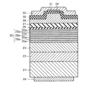
第1実施形態による窒化物系半導体発光ダイオード素子では、図1に示すように、サファイア基板1の(0001)面上に、約10nmの膜厚を有するAlGaNからなる低温バッファ層2が形成されている。なお、サファイア基板1は、本発明の「基板」および「絶縁性基板」の一例である。そして、低温バッファ層2上には、約1μmの膜厚を有するアンドープGaNからなる高温バッファ層3が形成されている。高温バッファ層3上には、約5μmの膜厚を有するSiがドープされたn型GaNからなるn型コンタクト層4が形成されている。また、n型コンタクト層4は、一部領域が除去されることによって、凸形状に形成されている。このn型コンタクト層4は、n型クラッド層としての機能も有する。なお、n型コンタクト層4は、本発明の「第1窒化物系半導体層」の一例である。
In the nitride-based semiconductor light-emitting diode device according to the first embodiment, as shown in FIG. 1, a low-
また、n型コンタクト層4の凸部上のほぼ全面と接触するように、約5nmの膜厚を有する6つのアンドープIn0.15Ga0.85Nからなる障壁層5aと、約5nmの膜厚を有する5つのアンドープIn0.35Ga0.65Nからなる井戸層5bとが交互に積層された多重量子井戸(MQW:Multiple Quantum Well)構造を有するMQW活性層5が形成されている。なお、MQW活性層5は、本発明の「活性層」の一例である。そして、MQW活性層5上には、約10nmの膜厚を有するアンドープGaNからなる保護層6が形成されている。この保護層6は、MQW活性層5のInが脱離するのを防止することによりMQW活性層5の結晶の劣化を防止する機能を有する。
Further, six undoped In 0.15 Ga 0.85 N barrier layers 5 a having a film thickness of about 5 nm and a film of about 5 nm so as to be in contact with almost the entire surface of the n-
ここで、第1実施形態では、保護層6上に、約0.15μmの膜厚を有するとともに、約3×1019cm−3のドーピング量および約1×1018cm−3のキャリア濃度を有するMgがドープされたp型Al0.05Ga0.95Nからなるp型クラッド層7が形成されている。なお、p型クラッド層7は、本発明の「第2窒化物系半導体層」および「クラッド層」の一例である。また、第1実施形態では、p型クラッド層7上に、約1nm〜約10nmの膜厚を有するアンドープIn0.15Ga0.85Nからなるアンドープコンタクト層8が形成されている。このIn0.15Ga0.85Nからなるアンドープコンタクト層8のバンドギャップは、Al0.05Ga0.95Nからなるp型クラッド層7のバンドギャップよりも小さく、かつ、アンドープIn0.15Ga0.85NとアンドープIn0.35Ga0.65NとからなるMQW活性層5のバンドギャップよりも大きい。なお、MQW活性層5のバンドギャップは、伝導帯および価電子帯に形成される2つの量子準位(基底準位)間のエネルギ差を意味し、In0.15Ga0.85NとIn0.35Ga0.65Nとで構成されるMQW活性層5の量子準位間のエネルギ差は、In0.15Ga0.85Nからなるアンドープコンタクト層8のバンドギャップよりも小さくなる。
また、アンドープコンタクト層8の上面上には、下から上に向かって、約100nmの膜厚を有するPd膜と、約100nmの膜厚を有するAu膜とから構成されるくし状のp側電極9が形成されている。なお、p側電極9は、本発明の「電極」の一例である。
Here, in the first embodiment, the
Further, on the upper surface of the
図3は、図1に示した第1実施形態による窒化物系半導体発光ダイオード素子において、コンタクト層の材料と厚みとを変化させた場合のp側電極とコンタクト層とのコンタクト抵抗を示したグラフである。この図3に示すグラフには、約1×1018cm−3のキャリア濃度を有するMgがドープされたp型GaN層をコンタクト層として用いた場合のコンタクト抵抗との相対値が示されている。なお、Mgがドープされたp型GaNは、コンタクト層に標準的に用いられる材料である。 FIG. 3 is a graph showing the contact resistance between the p-side electrode and the contact layer when the material and thickness of the contact layer are changed in the nitride-based semiconductor light-emitting diode device according to the first embodiment shown in FIG. It is. The graph shown in FIG. 3 shows a relative value with respect to the contact resistance when a p-type GaN layer doped with Mg having a carrier concentration of about 1 × 10 18 cm −3 is used as a contact layer. . Note that p-type GaN doped with Mg is a standard material used for the contact layer.
図3に示すように、アンドープIn0.15Ga0.85Nからなるアンドープコンタクト層8の膜厚を約1nm〜約10nmにすることによって、アンドープコンタクト層8のコンタクト抵抗を、Mgがドープされたp型GaNからなるp型コンタクト層のコンタクト抵抗に近づけることができることがわかる。また、アンドープGaNからなるアンドープコンタクト層を設けた場合でも、膜厚を約1nm〜約10nmにすることによって、ある程度コンタクト抵抗を小さくすることができることがわかる。ただし、アンドープIn0.15Ga0.85Nからなるアンドープコンタクト層8の方が、アンドープGaNからなるアンドープコンタクト層よりもコンタクト抵抗をより小さくすることができる。上記の点を考慮して、第1実施形態では、約1nm〜約10nmの膜厚を有するアンドープIn0.15Ga0.85Nからなるアンドープコンタクト層8を用いている。なお、アンドープAl0.05Ga0.95Nからなるアンドープコンタクト層では、膜厚を約1nm〜約10nmにしたとしても、コンタクト抵抗が大きいことがわかる。また、p型Al0.15Ga0.85Nからなるp型コンタクト層のコンタクト抵抗は、p型GaNからなるp型コンタクト層のコンタクト抵抗の約10倍であり、高いことがわかる。
As shown in FIG. 3, by setting the thickness of the
また、図1および図2に示すように、p側電極9の上面上の一部領域には、下から上に向かって、約30nmの膜厚を有するTi膜と、約500nmの膜厚を有するAu膜とから構成されるp側パッド電極10が形成されている。また、n型コンタクト層4の表面上の凸部以外の一部領域には、約500nmの膜厚を有するAlからなるn側電極11が形成されている。
As shown in FIGS. 1 and 2, in a partial region on the upper surface of the p-
第1実施形態では、上記のように、アンドープコンタクト層8を設けることによって、アンドープコンタクト層8には不純物準位が形成されないので、不純物準位に起因する光吸収を防止することができる。また、アンドープコンタクト層8には、不純物のドープに起因する結晶欠陥がないので、アンドープコンタクト層8は、良好な結晶性を有する。このため、アンドープコンタクト層8の結晶欠陥に起因する光吸収も抑制することができる。これにより、アンドープコンタクト層8での光吸収損失を低減することができるので、窒化物系半導体発光ダイオード素子の発光効率を向上させることができる。
In the first embodiment, as described above, by providing the
また、第1実施形態では、上記のように、アンドープコンタクト層8のバンドギャップをp型クラッド層7のバンドギャップよりも小さくすることによって、アンドープコンタクト層8とp側電極9との界面におけるエネルギ障壁が小さくなるので、アンドープコンタクト層8とp側電極9とのオーミック接触を実現しやすくすることができる。これにより、窒化物系半導体発光ダイオード素子の発光効率をより向上することができるとともに、駆動電圧を低くすることができる。
In the first embodiment, as described above, the energy at the interface between the
また、第1実施形態では、上記のように、アンドープコンタクト層8の膜厚を約1nm〜約10nmにすることによって、アンドープコンタクト層8とp側電極9との間のコンタクト抵抗を低減することができるので、アンドープコンタクト層8とp側電極9との間で良好なオーミック接触を得ることができる。また、アンドープコンタクト層8の抵抗を低減することができる。
In the first embodiment, as described above, the contact resistance between the
また、第1実施形態では、上記のように、p型クラッド層7をMgがドープされたp型Al0.05Ga0.95Nにより形成することによって、p型クラッド層7のバンドギャップを容易に大きくすることができるので、p型クラッド層7における光吸収を低減することができる。さらに、第1実施形態では、アンドープコンタクト層8をIn0.15Ga0.85Nにより形成することによって、容易に、アンドープコンタクト層8のバンドギャップをp型クラッド層7よりも小さくすることができる。また、上記のように、アンドープコンタクト層8のバンドギャップがMQW活性層5のバンドギャップよりも大きくなるので、容易に、アンドープコンタクト層8での光吸収を低減することができる。
In the first embodiment, as described above, the p-
図4および図5は、図1および図2に示した第1実施形態による窒化物系半導体発光ダイオード素子の製造プロセスを説明するための断面図である。次に、図1、図2、図4および図5を参照して、第1実施形態による窒化物系半導体発光ダイオード素子の製造プロセスについて説明する。 4 and 5 are cross-sectional views for explaining a manufacturing process of the nitride-based semiconductor light-emitting diode device according to the first embodiment shown in FIGS. A manufacturing process for the nitride-based semiconductor light-emitting diode device according to the first embodiment is now described with reference to FIGS.
まず、図4に示すように、MOVPE法(Metal Organic Vapor Phase Epitaxy:有機金属気相成長法)を用いて、サファイア基板1上に、低温バッファ層2、高温バッファ層3、n型コンタクト層4、MQW活性層5、保護層6、p型クラッド層7およびアンドープコンタクト層8を順次成長させる。
First, as shown in FIG. 4, a low-
具体的には、サファイア基板1を約600℃の非単結晶成長温度に保持した状態で、H2およびN2からなるキャリアガス(H2:約50%)と、NH3、トリメチルアルミニウム(TMAl)およびトリメチルガリウム(TMGa)からなる原料ガスとを用いて、サファイア基板1の(0001)面上に、約10nmの膜厚を有するAlGaNからなる低温バッファ層2を成長させる。
Specifically, with the sapphire substrate 1 held at a non-single crystal growth temperature of about 600 ° C., a carrier gas (H 2 : about 50%) composed of H 2 and N 2 , NH 3 , trimethylaluminum (TMAl ) And a source gas made of trimethylgallium (TMGa), a low-
次に、基板温度を約1150℃の単結晶成長温度に保持した状態で、H2およびN2からなるキャリアガス(H2:約50%)と、NH3およびTMGaからなる原料ガスとを用いて、約1μm/hの成長速度で、低温バッファ層2上に、約1μmの膜厚を有するアンドープGaNからなる高温バッファ層3を成長させる。
Next, a carrier gas composed of H 2 and N 2 (H 2 : about 50%) and a source gas composed of NH 3 and TMGa are used with the substrate temperature maintained at a single crystal growth temperature of about 1150 ° C. Thus, the high
次に、基板温度を約1150℃の単結晶成長温度に保持した状態で、H2およびN2からなるキャリアガス(H2:約50%)と、NH3およびTMGaからなる原料ガスと、SiH4からなるドーパントガスとを用いて、約3μm/hの成長速度で、高温バッファ層3上に、約5μmの膜厚を有するSiがドープされたn型GaNからなるn型コンタクト層4を成長させる。
Next, with the substrate temperature maintained at a single crystal growth temperature of about 1150 ° C., a carrier gas composed of H 2 and N 2 (H 2 : about 50%), a source gas composed of NH 3 and TMGa, and SiH using a dopant gas comprising 4, grown at a growth rate of about 3 [mu] m / h, on the high-
次に、基板温度を約850℃の単結晶成長温度に保持した状態で、H2およびN2からなるキャリアガス(H2:約1%〜約5%)と、NH3、トリエチルガリウム(TEGa)およびトリメチルインジウム(TMIn)からなる原料ガスとを用いて、約0.4nm/sの成長速度で、n型コンタクト層4上に、約5nmの膜厚を有する6つのアンドープIn0.15Ga0.85Nからなる障壁層5aと、約5nmの膜厚を有する5つのアンドープIn0.35Ga0.65Nからなる井戸層5bとを交互に成長させる。これにより、n型コンタクト層4上にMQW活性層5が形成される。続いて、MQW活性層5上に、約0.4nm/sの成長速度で、約10nmの膜厚を有するアンドープGaNからなる保護層6を成長させる。
Next, with the substrate temperature maintained at a single crystal growth temperature of about 850 ° C., a carrier gas composed of H 2 and N 2 (H 2 : about 1% to about 5%), NH 3 , triethyl gallium (TEGa) And 6 undoped In 0.15 Ga having a film thickness of about 5 nm on the n-
次に、基板温度を約1150℃の単結晶成長温度に保持した状態で、H2およびN2からなるキャリアガス(H2:約1%〜約3%)と、NH3、TMGaおよびTMAlからなる原料ガスと、シクロペンタジエニルマグネシウム(Cp2Mg)からなるドーパントガスとを用いて、約3μm/hの成長速度で、保護層6上に、約0.15μmの膜厚を有するとともに、約3×1019cm−3のドーピング量および約1×1018cm−3のキャリア濃度を有するMgがドープされたp型Al0.05Ga0.95Nからなるp型クラッド層7を成長させる。
Next, with the substrate temperature maintained at a single crystal growth temperature of about 1150 ° C., a carrier gas composed of H 2 and N 2 (H 2 : about 1% to about 3%) and NH 3 , TMGa and TMAl And having a film thickness of about 0.15 μm on the
この際、キャリアガスのH2組成を約1%〜約3%と低くすることによって、アクセプタとしてのMgを活性化させることができるので、高いキャリア濃度を有するp型クラッド層7を得ることができる。
At this time, Mg as an acceptor can be activated by lowering the H 2 composition of the carrier gas to about 1% to about 3%, so that the p-
次に、基板温度を約850℃の単結晶成長温度に保持した状態で、H2およびN2からなるキャリアガス(H2:約1%〜約5%)と、NH3、TEGaおよびTMInからなる原料ガスとを用いて、約3μm/hの成長速度で、p型クラッド層7上に、約1nm〜約10nmの膜厚を有するアンドープIn0.15Ga0.85Nからなるアンドープコンタクト層8を成長させる。
Next, with the substrate temperature maintained at a single crystal growth temperature of about 850 ° C., a carrier gas composed of H 2 and N 2 (H 2 : about 1% to about 5%), NH 3 , TEGa and TMIn And an undoped contact layer made of undoped In 0.15 Ga 0.85 N having a thickness of about 1 nm to about 10 nm on the p-
そして、図5に示すように、反応性イオンビームエッチング(RIBE)法などを用いて、アンドープコンタクト層8、p型クラッド層7、保護層6、MQW活性層5およびn型コンタクト層4の一部領域を除去することにより、n型コンタクト層4の一部領域を露出させる。
Then, as shown in FIG. 5, one of the
次に、図1および図2に示したように、真空蒸着法などを用いて、アンドープコンタクト層8の上面上に、下から上に向かって、約100nmの膜厚を有するPd膜と、約100nmの膜厚を有するAu膜とから構成されるくし状のp側電極9を形成する。そのp側電極9の上面上の一部領域に、下から上に向かって、約30nmの膜厚を有するTi膜と、約500nmの膜厚を有するAu膜とから構成されるp側パッド電極10を形成する。また、n型コンタクト層4の露出された表面上に、約500nmの膜厚を有するAlからなるn側電極11を形成する。
Next, as shown in FIGS. 1 and 2, using a vacuum deposition method or the like, a Pd film having a thickness of about 100 nm is formed on the upper surface of the
その後、約600℃の温度で熱処理することによって、p側電極9およびn側電極11を、それぞれ、アンドープコンタクト層8およびn型コンタクト層4にオーミック接触させる。
Thereafter, the p-
最後に、スクライブ、ダイシングおよびブレーキングなどの方法を用いて、たとえば、一辺の長さが約400μmのほぼ正方形のチップ形状になるように素子分離を行う。このようにして、第1実施形態の窒化物系半導体発光ダイオード素子が形成される。 Finally, element separation is performed using a method such as scribing, dicing, and braking so as to form a substantially square chip having a side length of about 400 μm, for example. Thus, the nitride-based semiconductor light-emitting diode element of the first embodiment is formed.
さらに、上記のように形成された第1実施形態の窒化物系半導体発光ダイオード素子(青色LEDチップ)をフレーム(図示せず)に固定した後、それらを覆うように、樹脂を200℃前後の温度で硬化させることによって、第1実施形態の青色LEDチップを含むLEDランプを作製してもよい。 Furthermore, after fixing the nitride-based semiconductor light-emitting diode element (blue LED chip) of the first embodiment formed as described above to a frame (not shown), a resin is coated at around 200 ° C. so as to cover them. An LED lamp including the blue LED chip of the first embodiment may be manufactured by curing at a temperature.
(第2実施形態)
図6は、本発明の第2実施形態による窒化物系半導体レーザ素子(LDチップ)を示した断面図である。図6を参照して、この第2実施形態では、窒化物系半導体発光ダイオード素子に本発明を適用した第1実施形態と異なり、窒化物系半導体レーザ素子に本発明を適用した例について説明する。
(Second Embodiment)
FIG. 6 is a sectional view showing a nitride-based semiconductor laser device (LD chip) according to the second embodiment of the present invention. Referring to FIG. 6, in the second embodiment, an example in which the present invention is applied to a nitride semiconductor laser element will be described, unlike the first embodiment in which the present invention is applied to a nitride semiconductor light emitting diode element. .
この第2実施形態による窒化物系半導体レーザ素子では、図6に示すように、(0001)Ga面を表面とする酸素がドープされた導電性のn型GaN基板21上に、約1μmの膜厚を有するSiがドープされたn型GaN層22が形成されている。n型GaN層22上には、約1μmの膜厚を有するSiがドープされたn型Al0.15Ga0.85Nからなるn型クラッド層23が形成されている。なお、n型GaN基板21は、本発明の「基板」の一例であり、n型GaN層22およびn型クラッド層23は、本発明の「第1窒化物系半導体層」の一例である。
In the nitride-based semiconductor laser device according to the second embodiment, as shown in FIG. 6, a film of about 1 μm is formed on a conductive n-
また、n型クラッド層23上には、約100nmの膜厚を有するn型GaNからなるn型光ガイド層24が形成されている。そして、n型光ガイド層24上には、約15nmの膜厚を有する4つのアンドープIn0.05Ga0.95Nからなる障壁層25aと、約4nmの膜厚を有する3つのアンドープIn0.1Ga0.9Nからなる井戸層25bとが交互に積層された多重量子井戸構造を有するMQW活性層25が形成されている。
On the n-
ここで、第2実施形態では、MQW活性層25上に、約20nmの膜厚を有するアンドープAl0.3Ga0.7Nからなる保護層26が形成されている。この保護層26は、MQW活性層25のInが脱離するのを防止することによりMQW活性層25の結晶の劣化を防止する機能を有する。また、保護層26上には、約100nmの膜厚を有するアンドープGaNからなる光ガイド層27が形成されている。そして、アンドープGaNからなる光ガイド層27は、後述するAl0.15Ga0.85Nからなるp型クラッド層28のバンドギャップよりも小さいバンドギャップを有する。なお、光ガイド層27は、本発明の「第3窒化物系半導体層」の一例である。
Here, in the second embodiment, the
そして、光ガイド層27上には、約280nmの膜厚を有するとともに、中央部付近に約1.5μmの幅を有するストライプ状の凸部を有するMgがドープされたp型Al0.15Ga0.85Nからなるp型クラッド層28が形成されている。なお、p型クラッド層28は、本発明の「第2窒化物系半導体層」および「クラッド層」の一例である。
On the
ここで、第2実施形態では、p型Al0.15Ga0.85Nからなるp型クラッド層28の凸部上に、約5nmの膜厚を有するアンドープIn0.05Ga0.95Nからなるアンドープコンタクト層29が形成されている。そして、p型クラッド層28の凸部とアンドープコンタクト層29とによって、電流通路領域となるリッジ部が構成されている。このアンドープコンタクト層29のバンドギャップは、p型クラッド層28のバンドギャップよりも小さく、かつ、MQW活性層25のバンドギャップよりも大きい。なお、MQW活性層25のバンドギャップは、伝導帯および価電子帯に形成される2つの量子準位(基底準位)間のエネルギ差を意味し、In0.05Ga0.95NとIn0.1Ga0.9Nとで構成されるMQW活性層25の量子準位間のエネルギ差は、In0.05Ga0.95Nからなるアンドープコンタクト層29のバンドギャップよりも小さくなる。
Here, in the second embodiment, undoped In 0.05 Ga 0.95 N having a film thickness of about 5 nm on the convex portion of the p-
また、p型クラッド層28の表面とアンドープコンタクト層29の側面とを覆うように、SiO2からなる絶縁膜30が形成されている。そして、アンドープコンタクト層29上には、下から上に向かって、Pd膜と、Pt膜と、Au膜とから構成されるp側電極31が形成されている。なお、p側電極31は、本発明の「電極」の一例である。また、絶縁膜30の表面とp側電極31の表面とを覆うように、p側パッド電極32が形成されている。そして、n型GaN基板21の裏面上には、n型GaN基板21の裏面に近い側から、Ti膜と、Pt膜と、Au膜とから構成されるn側電極33が形成されている。
An insulating
第2実施形態では、上記のように、アンドープコンタクト層29を設けることによって、アンドープコンタクト層29には不純物準位が形成されないので、不純物準位に起因する光吸収を防止することができる。また、アンドープコンタクト層29には、不純物のドープに起因する結晶欠陥がないので、良好な結晶性を有する。このため、アンドープコンタクト層29の結晶欠陥に起因する光吸収も抑制することができる。これにより、アンドープコンタクト層29での光吸収損失を低減することができるので、窒化物系半導体レーザ素子の発光効率を向上させることができる。
In the second embodiment, as described above, by providing the
また、第2実施形態では、上記のように、アンドープコンタクト層29のバンドギャップをp型クラッド層28のバンドギャップよりも小さくすることによって、アンドープコンタクト層29とp側電極31との界面におけるエネルギ障壁が小さくなるので、アンドープコンタクト層29とp側電極31とのオーミック接触を実現しやすくすることができる。
In the second embodiment, as described above, the energy at the interface between the
また、第2実施形態では、上記のように、p型クラッド層28をMgがドープされたp型Al0.15Ga0.85Nにより形成することによって、p型クラッド層28のバンドギャップを容易に大きくすることができるので、p型クラッド層28における光吸収を容易に低減することができる。さらに、第2実施形態では、アンドープコンタクト層29をIn0.05Ga0.95Nにより形成することによって、容易に、アンドープコンタクト層29のバンドギャップをp型クラッド層28よりも小さくすることができる。また、上記のように、アンドープコンタクト層29のバンドギャップがMQW活性層25のバンドギャップよりも大きくなるので、容易に、アンドープコンタクト層29での光吸収を低減することができる。
In the second embodiment, as described above, the p-
また、第2実施形態では、上記のように、MQW活性層25とp型クラッド層28との間に、p型クラッド層28のバンドギャップよりも小さいバンドギャップを有するアンドープの光ガイド層27を設けることによって、光ガイド層27により光の閉じ込め特性などの発光特性を制御することができるとともに、光ガイド層27での光吸収も抑制することができる。
In the second embodiment, as described above, the undoped
図7〜図9は、図6に示した第2実施形態による窒化物系半導体レーザ素子の製造プロセスを説明するための断面図である。次に、図6〜図9を参照して、第2実施形態による窒化物系半導体レーザ素子の製造プロセスについて説明する。 7 to 9 are cross-sectional views for explaining a manufacturing process of the nitride-based semiconductor laser device according to the second embodiment shown in FIG. A manufacturing process for the nitride-based semiconductor laser device according to the second embodiment is now described with reference to FIGS.
まず、図7に示すように、MOVPE法を用いて、(0001)Ga面を表面とする酸素がドープされたn型GaN基板21上に、n型GaN層22、n型クラッド層23、n型光ガイド層24、MQW活性層25、保護層26、光ガイド層27、p型クラッド層28およびアンドープコンタクト層29を順次成長させる。
First, as shown in FIG. 7, an n-
具体的には、n型GaN基板21を約1150℃の成長温度に保持した状態で、H2およびN2からなるキャリアガス(H2:約50%)と、NH3およびTMGaからなる原料ガスと、SiH4からなるドーパントガスとを用いて、約3μm/hの成長速度で、(0001)Ga面を表面とする酸素がドープされたn型GaN基板21上に、約1μmの膜厚を有するSiがドープされたn型GaN層22を成長させる。
Specifically, with the n-
次に、基板温度を約1150℃の成長温度に保持した状態で、H2およびN2からなるキャリアガス(H2:約50%)と、NH3、TMGaおよびTMAlからなる原料ガスと、SiH4からなるドーパントガスとを用いて、約3μm/hの成長速度で、n型GaN層22上に、約1μmの膜厚を有するSiがドープされたn型Al0.15Ga0.85Nからなるn型クラッド層23を成長させる。続いて、n型クラッド層23上に、約3μm/hの成長速度で、約100nmの膜厚を有するn型GaNからなるn型光ガイド層24を成長させる。
Next, with the substrate temperature maintained at a growth temperature of about 1150 ° C., a carrier gas composed of H 2 and N 2 (H 2 : about 50%), a source gas composed of NH 3 , TMGa and TMAl, and SiH using a dopant gas comprising 4, at a growth rate of about 3 [mu] m / h, on the n-
次に、基板温度を約850℃の成長温度に保持した状態で、H2およびN2からなるキャリアガス(H2:約1%〜約5%)と、NH3、TEGaおよびTMInからなる原料ガスとを用いて、約0.4nm/sの成長速度で、n型光ガイド層24上に、約15nmの膜厚を有する4つのアンドープIn0.05Ga0.95Nからなる障壁層25aと、約4nmの膜厚を有する3つのアンドープIn0.1Ga0.9Nからなる井戸層25bとを交互に成長させる。これにより、n型光ガイド層24上に、MQW活性層25が形成される。続いて、MQW活性層25上に、約0.4nm/sの成長速度で、約20nmの膜厚を有するアンドープAl0.3Ga0.7Nからなる保護層26を成長させる。
Next, in a state where the substrate temperature is maintained at a growth temperature of about 850 ° C., a carrier gas (H 2 : about 1% to about 5%) made of H 2 and N 2 and a raw material made of NH 3 , TEGa and TMIn And a
次に、基板温度を約1150℃の成長温度に保持した状態で、H2およびN2からなるキャリアガス(H2:約1%〜約3%)と、NH3およびTMGaからなる原料ガスとを用いて、約3μm/hの成長速度で、保護層26上に、約100nmの膜厚を有するアンドープGaNからなる光ガイド層27を成長させる。さらに、TMAlからなる原料ガスを加えるとともに、Cp2Mgからなるドーパントガスを加えて、光ガイド層27上に、約3μm/hの成長速度で、約280nmの膜厚を有するMgがドープされたp型Al0.15Ga0.85Nからなるp型クラッド層28を成長させる。
Next, with the substrate temperature maintained at a growth temperature of about 1150 ° C., a carrier gas consisting of H 2 and N 2 (H 2 : about 1% to about 3%), a source gas consisting of NH 3 and TMGa, The
この際、キャリアガスのH2組成を約1%〜約3%と低くすることによって、アクセプタとしてのMgを活性化させることができるので、高いキャリア濃度を有するp型クラッド層28を得ることができる。
At this time, Mg as an acceptor can be activated by lowering the H 2 composition of the carrier gas to about 1% to about 3%, so that the p-
次に、基板温度を約850℃の成長温度に保持した状態で、H2およびN2からなるキャリアガス(H2:約1%〜約5%)と、NH3、TEGaおよびTMInからなる原料ガスとを用いて、約3μm/hの成長速度で、p型クラッド層28上に、約5nmの膜厚を有するアンドープIn0.05Ga0.95Nからなるアンドープコンタクト層29を成長させる。
Next, in a state where the substrate temperature is maintained at a growth temperature of about 850 ° C., a carrier gas (H 2 : about 1% to about 5%) made of H 2 and N 2 and a raw material made of NH 3 , TEGa and TMIn An
そして、図8に示すように、真空蒸着法およびリソグラフィ技術を用いて、アンドープコンタクト層29上の中央部付近に、下から上に向かって、Pd膜と、Pt膜と、Au膜とから構成されるp側電極31を、約1.5μmの幅を有するストライプ状に形成する。
Then, as shown in FIG. 8, a Pd film, a Pt film, and an Au film are formed in the vicinity of the central portion on the
この後、図9に示すように、反応性イオンビームエッチング法などを用いて、p側電極31をマスクとして、アンドープコンタクト層29およびp型クラッド層28の一部領域を除去する。これにより、電流注入領域となる凸部(リッジ部)が形成される。
Thereafter, as shown in FIG. 9, a partial region of the
次に、プラズマCVD法(Chemical Vapor Deposition:化学的気相堆積法)を用いて、p型クラッド層28の表面とアンドープコンタクト層29の表面とp側電極31の表面とを覆うように、SiO2からなる絶縁膜(図示せず)を形成した後、p側電極31の表面上の絶縁膜を除去することによって、図6に示すような形状を有する絶縁膜30が得られる。そして、絶縁膜30の表面とp側電極31の表面とを覆うように、p側パッド電極32を形成する。
Next, the surface of the p-
最後に、n型GaN基板21を所定の厚み(たとえば、約100μm)になるまで研磨した後、真空蒸着法を用いて、n型GaN基板21の裏面上に、n型GaN基板21の裏面に近い側から、Ti膜と、Pt膜と、Au膜とから構成されるn側電極33を形成する。このようにして、第2実施形態の窒化物系半導体レーザ素子が形成される。
Finally, after polishing the n-
(第3実施形態)
図10は、本発明の第3実施形態による窒化物系半導体発光ダイオード素子(青色LEDチップ)を示した断面図である。図10を参照して、この第3実施形態では、上記第1実施形態において形成された高温バッファ層3に代えて、より低転位のアンドープGaN層44を形成した例について説明する。なお、その他の構成は、第1実施形態と同様である。
(Third embodiment)
FIG. 10 is a cross-sectional view illustrating a nitride-based semiconductor light-emitting diode device (blue LED chip) according to a third embodiment of the present invention. Referring to FIG. 10, in the third embodiment, an example in which an
すなわち、第3実施形態による窒化物系半導体発光ダイオード素子では、図10に示すように、サファイア基板41の(0001)面上に、約10nm〜約1000nmの膜厚を有するSiNからなる断面が逆メサ形状(逆台形状)のマスク層42が、約7μmの周期でストライプ状(細長状)に形成されている。なお、サファイア基板41は、本発明の「基板」および「絶縁性基板」の一例である。そして、マスク層42は、隣接するマスク層42間の最短距離が、マスク層42間に露出したサファイア基板41の幅よりも小さくなるように形成されている。
That is, in the nitride-based semiconductor light-emitting diode device according to the third embodiment, the cross section made of SiN having a film thickness of about 10 nm to about 1000 nm on the (0001) plane of the
また、マスク層42間に露出したサファイア基板41上には、約10nm〜約50nmの膜厚を有するAlGaNまたはGaNからなる低温バッファ層43が形成されている。そして、低温バッファ層43上およびマスク層42上には、選択横方向成長を用いて、マスク層42間を埋め込むように、約2μmの膜厚を有する低転位のアンドープGaN層44が形成されている。なお、アンドープGaN層44は、本発明の「第5窒化物系半導体層」の一例である。
A low
そして、アンドープGaN層44上に形成されているn型コンタクト層4、MQW活性層5、保護層6、p型クラッド層7、アンドープコンタクト層8、p側電極9、p側パッド電極10およびn側電極11の膜厚および組成は、図1に示した第1実施形態と同様である。
Then, the n-
第3実施形態では、上記のように、第1実施形態の高温バッファ層3(図1参照)よりも低転位のアンドープGaN層44上に、窒化物系半導体各層(4〜8)を形成することによって、窒化物系半導体各層(4〜8)に結晶欠陥が発生するのをより抑制することができる。これにより、結晶欠陥がより低減された窒化物系半導体各層(4〜8)を形成することができるので、結晶欠陥に起因する光吸収をより抑制することができる。その結果、より発光効率の高い青色LEDチップを形成することができる。
In the third embodiment, as described above, the nitride-based semiconductor layers (4 to 8) are formed on the
なお、第3実施形態のその他の効果は、第1実施形態と同様である。 The remaining effects of the third embodiment are similar to those of the first embodiment.
図11〜図13は、図10に示した第3実施形態による窒化物系半導体発光ダイオード素子の製造プロセスを説明するための断面図である。次に、図10〜図13を参照して、第3実施形態による窒化物系半導体発光ダイオード素子の製造プロセスについて説明する。 11 to 13 are cross-sectional views illustrating a manufacturing process of the nitride-based semiconductor light-emitting diode device according to the third embodiment shown in FIG. A manufacturing process for the nitride-based semiconductor light-emitting diode device according to the third embodiment is now described with reference to FIGS.
まず、図11に示すように、サファイア基板41上の全面にSiN膜(図示せず)を形成した後、そのSiN膜の所定領域上にレジスト(図示せず)を形成する。そして、そのレジストをマスクとして、SiN膜をウェットエッチングすることによって、ストライプ状のマスク層42を形成する。このマスク層42は、オーバーハング部42aを有するように、逆メサ形状(逆台形状)に形成されている。また、マスク層42の開口部は、たとえば、サファイア基板41の[11−20]方向またはサファイア基板41の[1−100]方向に形成するのが好ましい。この後、マスク層42間に露出したサファイア基板41上に、約500℃〜約700℃の成長温度で、約10nm〜約50nmの膜厚を有するAlGaNまたはGaNからなる低温バッファ層43を選択成長させる。
First, as shown in FIG. 11, after a SiN film (not shown) is formed on the entire surface of the
次に、MOVPE法を用いて、マスク層42を選択成長マスクとして、低温バッファ層43上に、約950℃〜約1200℃の成長温度で、アンドープGaN層44(図13参照)を横方向成長させる。この場合、露出された低温バッファ層43の上面上において、アンドープGaN層44は、まず、上方向に成長する。これにより、図12に示すように、成長初期の段階から、マスク層42間の中央部付近に、断面が三角形状のファセット構造のアンドープGaN層44aが成長される。また、マスク層42のオーバーハング部42aの下方には、アンドープGaN層44aよりも小さいファセット構造のアンドープGaN層44bが形成される。さらに、アンドープGaN層44aおよび44bからなるファセットの成長が進むと、各アンドープGaN層44aおよび44bは、横方向に成長して合体するとともに、マスク層42上にも成長される。これにより、図13に示すように、約2μmの膜厚を有する上面が平坦な連続膜からなるアンドープGaN層44が形成される。
Next, using the MOVPE method, the undoped GaN layer 44 (see FIG. 13) is laterally grown on the low
このように、アンドープGaN層44は、成長初期の段階から横方向に成長するので、アンドープGaN層44に発生する転位が成長初期の段階から横方向に曲げられる。これにより、より薄い厚みで、転位密度が約7×107cm−2に低減されたアンドープGaN層44を形成することができる。
Thus, since the
この後、第1実施形態と同様の製造プロセスを用いて、アンドープGaN層44上に、図10に示したような、n型コンタクト層4、MQW活性層5、保護層6、p型クラッド層7およびアンドープコンタクト層8を順次形成した後、n型コンタクト層4からアンドープコンタクト層8の一部領域を除去する。そして、アンドープコンタクト層8上に、p側電極9およびp側パッド電極10を順次形成する。この後、n型コンタクト層4の露出された表面上に、n側電極11を形成する。
Thereafter, using the same manufacturing process as in the first embodiment, the n-
最後に、スクライブ、ダイシングおよびブレーキングなどの方法を用いて、たとえば、一辺の長さが約400μmのほぼ正方形のチップ形状になるように素子分離を行う。このようにして、第3実施形態の窒化物系半導体発光ダイオード素子が形成される。 Finally, element separation is performed using a method such as scribing, dicing, and braking so as to form a substantially square chip having a side length of about 400 μm, for example. In this way, the nitride-based semiconductor light-emitting diode element of the third embodiment is formed.
(第4実施形態)
図14は、本発明の第4実施形態による窒化物系半導体レーザ素子(LDチップ)を示した断面図である。図14を参照して、この第4実施形態では、上記第2実施形態において形成されたn型光ガイド層24を設けない例について説明する。なお、その他の構成は、第2実施形態と同様である。
(Fourth embodiment)
FIG. 14 is a cross-sectional view showing a nitride-based semiconductor laser device (LD chip) according to the fourth embodiment of the present invention. With reference to FIG. 14, in the fourth embodiment, an example in which the n-type
すなわち、第4実施形態による窒化物系半導体レーザ素子では、図14に示すように、(0001)Ga面を表面とする酸素がドープされた導電性のn型GaN基板21上に、第2実施形態と同様の膜厚および組成を有するn型GaN層22およびn型クラッド層23が順次形成されている。
That is, in the nitride-based semiconductor laser device according to the fourth embodiment, as shown in FIG. 14, the second embodiment is performed on a conductive n-
ここで、第4実施形態では、n型クラッド層23の直上に、第2実施形態と同様の膜厚および組成を有する4つの障壁層25aと3つの井戸層25bとが交互に積層されたMQW活性層25が形成されている。すなわち、この第4実施形態では、n型クラッド層23とMQW活性層25との間には、n型光ガイド層が設けられていない。
Here, in the fourth embodiment, an MQW in which four
そして、MQW活性層25上に形成されている保護層26、光ガイド層27、p型クラッド層28、アンドープコンタクト層29、絶縁膜30、p側電極31およびp側パッド電極32の膜厚および組成は、図6に示した第2実施形態と同様である。また、n型GaN基板21の裏面上に形成されているn側電極33の膜厚および組成も、図6に示した第2実施形態と同様である。
The film thicknesses of the
第4実施形態では、上記のように、n型クラッド層23とMQW活性層25との間にn型光ガイド層を設けないことによって、MQW活性層25で生成された光の強度の高い領域がp側にずれるので、n型クラッド層23での光吸収が抑制される。この場合、光強度の高い領域がp側にずれたとしても、アンドープコンタクト層29にはドーピングに起因する不純物準位や結晶欠陥が形成されないので、光吸収が増大することがない。その結果、窒化物系半導体レーザ素子の発光効率の向上効果が大きくなる。
In the fourth embodiment, as described above, by providing no n-type light guide layer between the n-
なお、第4実施形態のその他の効果は、第2実施形態と同様である。 The remaining effects of the fourth embodiment are similar to those of the second embodiment.
図15〜図17は、図14に示した第4実施形態による窒化物系半導体レーザ素子の製造プロセスを説明するための断面図である。次に、図14〜図17を参照して、第4実施形態による窒化物系半導体レーザ素子の製造プロセスについて説明する。 15 to 17 are cross-sectional views for explaining the manufacturing process of the nitride-based semiconductor laser device according to the fourth embodiment shown in FIG. A manufacturing process for the nitride-based semiconductor laser device according to the fourth embodiment is now described with reference to FIGS.
まず、図15に示すように、MOCVD法を用いて、(0001)Ga面を表面とする酸素がドープされたn型GaN基板21上に、n型GaN層22およびn型クラッド層23を順次成長させる。次に、第4実施形態では、n型クラッド層23の直上に、4つの障壁層25aと3つの井戸層25bとを交互に成長させることによって、MQW活性層25を形成する。その後、MQW活性層25上に、保護層26、光ガイド層27、p型クラッド層28およびアンドープコンタクト層29を順次成長させる。なお、n型GaN層22、n型クラッド層23、MQW活性層25、保護層26、光ガイド層27、p型クラッド層28およびアンドープコンタクト層29を成長させる際の基板温度および導入ガスは、それぞれ、第2実施形態の基板温度および導入ガスと同様である。
First, as shown in FIG. 15, an n-
次に、図16に示すように、第2実施形態と同様、真空蒸着法およびリソグラフィ技術を用いて、アンドープコンタクト層29上の中央部付近に、ストライプ状のp側電極31を形成する。この後、反応性イオンビームエッチング法などを用いて、p側電極31をマスクとして、アンドープコンタクト層29およびp型クラッド層28の一部領域を除去することによって、図17に示すような電流通路領域となる凸状のリッジ部を形成する。
Next, as shown in FIG. 16, a striped p-
最後に、図14に示したように、第2実施形態と同様、プラズマCVD法を用いて、p型クラッド層28の表面とアンドープコンタクト層29の側面とを覆うように、絶縁膜30を形成した後、絶縁膜30の表面とp側電極31の表面とを覆うように、p側パッド電極32を形成する。この後、n型GaN基板21を所定の厚みになるまで研磨した後、真空蒸着法を用いて、n型GaN基板21の裏面上に、n側電極33を形成することによって、第4実施形態の窒化物系半導体レーザ素子が形成される。
Finally, as shown in FIG. 14, the insulating
なお、今回開示された実施形態は、すべての点で例示であって制限的なものではないと考えられるべきである。本発明の範囲は、上記した実施形態の説明ではなく特許請求の範囲によって示され、さらに特許請求の範囲と均等の意味および範囲内でのすべての変更が含まれる。 The embodiment disclosed this time should be considered as illustrative in all points and not restrictive. The scope of the present invention is shown not by the above description of the embodiments but by the scope of claims for patent, and further includes all modifications within the meaning and scope equivalent to the scope of claims for patent.
たとえば、上記第1〜第4実施形態では、基板として、サファイア基板およびn型GaN基板を用いるようにしたが、本発明はこれに限らず、スピネル基板、Si基板、SiC基板、GaAs基板、GaP基板、InP基板、水晶基板およびZrB2基板などを用いてもよい。 For example, in the first to fourth embodiments, the sapphire substrate and the n-type GaN substrate are used as the substrate. However, the present invention is not limited to this, and the spinel substrate, Si substrate, SiC substrate, GaAs substrate, GaP A substrate, an InP substrate, a quartz substrate, a ZrB 2 substrate, or the like may be used.
また、上記第1〜第4実施形態では、アンドープInGaNの単層からなるアンドープコンタクト層を形成するようにしたが、本発明はこれに限らず、図18に示すように、活性層のバンドギャップよりも大きいバンドギャップを有するアンドープInGaNなどからなる層を少なくとも1層含む複数のアンドープ層からなる超格子構造などの多層構造のp側コンタクト層49を形成するようにしてもよい。なお、p側コンタクト層49は、本発明の「アンドープコンタクト層」の一例である。この場合の超格子の構成としては、数nmの膜厚を有するアンドープInXGa1−XNからなる層と数nmの膜厚を有するアンドープInYGa1−YN(X>Y>0)からなる層との積層構造や、数nmの膜厚を有するアンドープInGaNからなる層と数nmの膜厚を有するアンドープAlGaN(GaNを含む)からなる層との積層構造などが考えられる。
In the first to fourth embodiments, an undoped contact layer made of a single layer of undoped InGaN is formed. However, the present invention is not limited to this, and as shown in FIG. A p-
また、上記第1〜第4実施形態では、窒化物系半導体の各層の表面が(0001)面になるように積層したが、本発明はこれに限らず、窒化物系半導体の各層の表面が他の方向になるように積層してもよい。たとえば、窒化物系半導体の各層の表面が(1−100)や(11−20)面などの(H、K、−H−K、0)面になるように積層してもよい。この場合、MQW活性層内にピエゾ電場が発生しないので、井戸層のエネルギバンドの傾きに起因する正孔と電子との再結合確率の低下を抑制することができる。その結果、MQW活性層の発光効率を向上することができる。 Moreover, in the said 1st-4th embodiment, it laminated | stacked so that the surface of each layer of a nitride-type semiconductor might become a (0001) plane, but this invention is not limited to this, The surface of each layer of a nitride-type semiconductor is You may laminate | stack so that it may become another direction. For example, the nitride semiconductor layers may be stacked such that the surface of each layer is a (H, K, -HK, 0) plane such as a (1-100) or (11-20) plane. In this case, since no piezoelectric field is generated in the MQW active layer, it is possible to suppress a decrease in the recombination probability between holes and electrons due to the inclination of the energy band of the well layer. As a result, the luminous efficiency of the MQW active layer can be improved.
また、上記第1〜第4実施形態では、活性層として多重量子井戸(MQW)構造を用いる例を示したが、本発明はこれに限らず、量子効果を有しない厚膜の単層または単一量子井戸構造であっても同様の効果を得ることができる。 In the first to fourth embodiments, an example in which a multiple quantum well (MQW) structure is used as the active layer has been described. However, the present invention is not limited to this, and the present invention is not limited to this. Similar effects can be obtained even with a single quantum well structure.
また、上記第1〜第4実施形態では、InGaNからなるアンドープコンタクト層をp側に設けるようにしたが、本発明はこれに限らず、GaNからなるアンドープコンタクト層をp側に設けるようにしてもよい。たとえば、第2実施形態による窒化物系半導体レーザ素子の構造において、InGaNからなるアンドープコンタクト層に代えて、GaNからなるアンドープコンタクト層を設けた場合には、図19に示すような構造となる。すなわち、第2実施形態と異なり、p型クラッド層28の凸部上には、GaNからなるアンドープコンタクト層59が形成されている。このように、GaNからなるアンドープコンタクト層59を設けた場合においても、光吸収を抑制することができるなどの第2実施形態と同様の効果を得ることができる。
In the first to fourth embodiments, the undoped contact layer made of InGaN is provided on the p side. However, the present invention is not limited to this, and the undoped contact layer made of GaN is provided on the p side. Also good. For example, in the structure of the nitride-based semiconductor laser device according to the second embodiment, when an undoped contact layer made of GaN is provided instead of the undoped contact layer made of InGaN, the structure shown in FIG. 19 is obtained. That is, unlike the second embodiment, an
また、上記第2実施形態では、n側およびp側に、それぞれ、同じ膜厚(約100nm)を有するn型光ガイド層24および光ガイド層27を設けるようにしたが、本発明はこれに限らず、図20に示すように、光ガイド層27の膜厚よりも小さい膜厚(たとえば、約50nm)を有するn型光ガイド層64を設けるようにしてもよい。この場合には、n型光ガイド層を設けない第4実施形態と同様の効果を得ることができる。すなわち、n型光ガイド層64の膜厚がp側の光ガイド層27の膜厚よりも小さい分、光強度の高い領域がp側にずれるので、n型クラッド層23での光吸収が抑制される。また、この場合には、第4実施形態と同様、ドーピングに起因する不純物準位や結晶欠陥が形成されないアンドープコンタクト層29で光吸収が増大することがないので、窒化物系半導体レーザ素子の発光効率の向上効果が大きくなる。
In the second embodiment, the n-type
1、41 サファイア基板(基板)
4 n型コンタクト層(第1窒化物系半導体層)
5、25 MQW活性層(活性層)
7、28 p型クラッド層(第2窒化物系半導体層、クラッド層)
8、29、59 アンドープコンタクト層
9、31 p側電極(電極)
21 n型GaN基板(基板)
22 n型GaN層(第1窒化物系半導体層)
23 n型クラッド層(第1窒化物系半導体層)
24、64 n型光ガイド層
27 光ガイド層(第3窒化物系半導体層)
49 p側コンタクト層(アンドープコンタクト層)
1, 41 Sapphire substrate (substrate)
4 n-type contact layer (first nitride semiconductor layer)
5, 25 MQW active layer (active layer)
7, 28 p-type cladding layer (second nitride semiconductor layer, cladding layer)
8, 29, 59
21 n-type GaN substrate (substrate)
22 n-type GaN layer (first nitride semiconductor layer)
23 n-type cladding layer (first nitride semiconductor layer)
24, 64 n-type
49 p-side contact layer (undoped contact layer)
Claims (11)
前記第1窒化物系半導体層上に形成され、窒化物系半導体層からなる活性層と、
前記活性層上に形成された第2導電型の第2窒化物系半導体層と、
前記第2窒化物系半導体層上に形成された窒化物系半導体からなるアンドープコンタクト層と、
前記アンドープコンタクト層上に形成された電極とを備えた、窒化物系半導体発光素子であって、
前記アンドープコンタクト層は、InGaNを含む、窒化物系半導体発光素子。 A first conductivity type first nitride-based semiconductor layer formed on a substrate;
An active layer formed on the first nitride-based semiconductor layer and made of a nitride-based semiconductor layer;
A second conductivity type second nitride semiconductor layer formed on the active layer;
An undoped contact layer made of a nitride semiconductor formed on the second nitride semiconductor layer;
A nitride-based semiconductor light-emitting device comprising an electrode formed on the undoped contact layer ,
The undoped contact layer is a nitride-based semiconductor light-emitting device containing InGaN.
前記第2導電型の第2窒化物系半導体層は、p型の第2窒化物系半導体層である、請求項1または2に記載の窒化物系半導体発光素子。 The first conductivity type first nitride semiconductor layer is an n-type first nitride semiconductor layer;
3. The nitride-based semiconductor light-emitting element according to claim 1, wherein the second conductivity-type second nitride-based semiconductor layer is a p-type second nitride-based semiconductor layer.
前記第4窒化物系半導体層は、前記第3窒化物系半導体層の膜厚よりも小さい膜厚を有する、請求項9〜10のいずれか1項に記載の窒化物系半導体発光素子。 A fourth nitride semiconductor layer formed between the active layer and the first conductivity type first nitride semiconductor layer;
11. The nitride-based semiconductor light-emitting element according to claim 9, wherein the fourth nitride-based semiconductor layer has a thickness smaller than that of the third nitride-based semiconductor layer.
Priority Applications (1)
| Application Number | Priority Date | Filing Date | Title |
|---|---|---|---|
| JP2003319528A JP4162560B2 (en) | 2002-09-18 | 2003-09-11 | Nitride semiconductor light emitting device |
Applications Claiming Priority (2)
| Application Number | Priority Date | Filing Date | Title |
|---|---|---|---|
| JP2002271968 | 2002-09-18 | ||
| JP2003319528A JP4162560B2 (en) | 2002-09-18 | 2003-09-11 | Nitride semiconductor light emitting device |
Related Child Applications (1)
| Application Number | Title | Priority Date | Filing Date |
|---|---|---|---|
| JP2008109596A Division JP5036617B2 (en) | 2002-09-18 | 2008-04-18 | Nitride semiconductor light emitting device |
Publications (2)
| Publication Number | Publication Date |
|---|---|
| JP2004134772A JP2004134772A (en) | 2004-04-30 |
| JP4162560B2 true JP4162560B2 (en) | 2008-10-08 |
Family
ID=32301696
Family Applications (1)
| Application Number | Title | Priority Date | Filing Date |
|---|---|---|---|
| JP2003319528A Expired - Fee Related JP4162560B2 (en) | 2002-09-18 | 2003-09-11 | Nitride semiconductor light emitting device |
Country Status (1)
| Country | Link |
|---|---|
| JP (1) | JP4162560B2 (en) |
Families Citing this family (12)
| Publication number | Priority date | Publication date | Assignee | Title |
|---|---|---|---|---|
| KR100568502B1 (en) | 2004-08-11 | 2006-04-07 | 한국전자통신연구원 | Semiconductor emission device |
| JP2006100475A (en) * | 2004-09-29 | 2006-04-13 | Toyoda Gosei Co Ltd | Semiconductor light emitting element |
| JP4967243B2 (en) * | 2005-03-08 | 2012-07-04 | 三菱化学株式会社 | GaN-based light emitting diode and light emitting device |
| JP4956902B2 (en) * | 2005-03-18 | 2012-06-20 | 三菱化学株式会社 | GaN-based light emitting diode and light emitting device using the same |
| KR100588377B1 (en) * | 2005-05-10 | 2006-06-09 | 삼성전기주식회사 | Vertically structured gan type light emitting diode and method of manufacturing the same |
| CN101449394A (en) * | 2006-05-26 | 2009-06-03 | 罗姆股份有限公司 | A nitride semiconductor luminous element |
| US20090179190A1 (en) * | 2006-05-26 | 2009-07-16 | Rohm Co., Ltd. | Nitride Semiconductor Light Emitting Element |
| JP5321656B2 (en) * | 2011-08-05 | 2013-10-23 | 三菱化学株式会社 | GaN-based light emitting diode and light emitting device |
| JP5304855B2 (en) * | 2011-08-12 | 2013-10-02 | 三菱化学株式会社 | GaN-based light emitting diode and light emitting device using the same |
| JP5733295B2 (en) * | 2012-12-04 | 2015-06-10 | 住友電気工業株式会社 | Nitride semiconductor light emitting device and method for manufacturing nitride semiconductor light emitting device |
| JPWO2016006298A1 (en) * | 2014-07-07 | 2017-04-27 | ソニー株式会社 | Semiconductor optical device |
| JP2021150373A (en) * | 2020-03-17 | 2021-09-27 | セイコーエプソン株式会社 | Light emitting device, projector, and display |
-
2003
- 2003-09-11 JP JP2003319528A patent/JP4162560B2/en not_active Expired - Fee Related
Also Published As
| Publication number | Publication date |
|---|---|
| JP2004134772A (en) | 2004-04-30 |
Similar Documents
| Publication | Publication Date | Title |
|---|---|---|
| JP5036617B2 (en) | Nitride semiconductor light emitting device | |
| US8101465B2 (en) | Method of fabricating a semiconductor device with a back electrode | |
| KR100267839B1 (en) | Nitride semiconductor device | |
| JP3864735B2 (en) | Semiconductor light emitting device and manufacturing method thereof | |
| JP3705047B2 (en) | Nitride semiconductor light emitting device | |
| KR100902109B1 (en) | Gallium nitride compound semiconductor element | |
| JP4304750B2 (en) | Nitride semiconductor growth method and nitride semiconductor device | |
| KR20030064629A (en) | Semiconductor light emitting device and its manufacturing method | |
| JP3660446B2 (en) | Nitride semiconductor device and manufacturing method thereof | |
| JPH11298090A (en) | Nitride semiconductor element | |
| JP2004111514A (en) | Nitride semiconductor light emitting element and its manufacturing method | |
| JP4162560B2 (en) | Nitride semiconductor light emitting device | |
| JP3973523B2 (en) | Nitride semiconductor laser device | |
| JP4291960B2 (en) | Nitride semiconductor device | |
| JP3651260B2 (en) | Nitride semiconductor device | |
| JP3896718B2 (en) | Nitride semiconductor | |
| KR100545999B1 (en) | nitride semiconductor device | |
| JPH11191639A (en) | Nitride semiconductor device | |
| JPH11191637A (en) | Nitride semiconductor device | |
| JP2000196201A (en) | Nitride semiconductor laser element | |
| JP4178807B2 (en) | Semiconductor light emitting device and manufacturing method thereof | |
| JP4423969B2 (en) | Nitride semiconductor multilayer substrate and nitride semiconductor device and nitride semiconductor laser device using the same | |
| KR100511530B1 (en) | The nitride semiconductor device | |
| JP3562478B2 (en) | Method for growing nitride semiconductor and device using the same | |
| JPH10326943A (en) | Nitride semiconductor element |
Legal Events
| Date | Code | Title | Description |
|---|---|---|---|
| A621 | Written request for application examination |
Free format text: JAPANESE INTERMEDIATE CODE: A621 Effective date: 20040702 |
|
| A977 | Report on retrieval |
Free format text: JAPANESE INTERMEDIATE CODE: A971007 Effective date: 20070205 |
|
| A131 | Notification of reasons for refusal |
Free format text: JAPANESE INTERMEDIATE CODE: A131 Effective date: 20070213 |
|
| A521 | Written amendment |
Free format text: JAPANESE INTERMEDIATE CODE: A523 Effective date: 20070403 |
|
| A131 | Notification of reasons for refusal |
Free format text: JAPANESE INTERMEDIATE CODE: A131 Effective date: 20080219 |
|
| A521 | Written amendment |
Free format text: JAPANESE INTERMEDIATE CODE: A523 Effective date: 20080418 |
|
| A521 | Written amendment |
Free format text: JAPANESE INTERMEDIATE CODE: A523 Effective date: 20080527 |
|
| TRDD | Decision of grant or rejection written | ||
| A01 | Written decision to grant a patent or to grant a registration (utility model) |
Free format text: JAPANESE INTERMEDIATE CODE: A01 Effective date: 20080624 |
|
| A01 | Written decision to grant a patent or to grant a registration (utility model) |
Free format text: JAPANESE INTERMEDIATE CODE: A01 |
|
| A61 | First payment of annual fees (during grant procedure) |
Free format text: JAPANESE INTERMEDIATE CODE: A61 Effective date: 20080722 |
|
| FPAY | Renewal fee payment (event date is renewal date of database) |
Free format text: PAYMENT UNTIL: 20110801 Year of fee payment: 3 |
|
| R151 | Written notification of patent or utility model registration |
Ref document number: 4162560 Country of ref document: JP Free format text: JAPANESE INTERMEDIATE CODE: R151 |
|
| FPAY | Renewal fee payment (event date is renewal date of database) |
Free format text: PAYMENT UNTIL: 20110801 Year of fee payment: 3 |
|
| FPAY | Renewal fee payment (event date is renewal date of database) |
Free format text: PAYMENT UNTIL: 20120801 Year of fee payment: 4 |
|
| FPAY | Renewal fee payment (event date is renewal date of database) |
Free format text: PAYMENT UNTIL: 20130801 Year of fee payment: 5 |
|
| R250 | Receipt of annual fees |
Free format text: JAPANESE INTERMEDIATE CODE: R250 |
|
| S111 | Request for change of ownership or part of ownership |
Free format text: JAPANESE INTERMEDIATE CODE: R313113 |
|
| FPAY | Renewal fee payment (event date is renewal date of database) |
Free format text: PAYMENT UNTIL: 20130801 Year of fee payment: 5 |
|
| R350 | Written notification of registration of transfer |
Free format text: JAPANESE INTERMEDIATE CODE: R350 |
|
| R250 | Receipt of annual fees |
Free format text: JAPANESE INTERMEDIATE CODE: R250 |
|
| R250 | Receipt of annual fees |
Free format text: JAPANESE INTERMEDIATE CODE: R250 |
|
| R250 | Receipt of annual fees |
Free format text: JAPANESE INTERMEDIATE CODE: R250 |
|
| S111 | Request for change of ownership or part of ownership |
Free format text: JAPANESE INTERMEDIATE CODE: R313113 |
|
| R350 | Written notification of registration of transfer |
Free format text: JAPANESE INTERMEDIATE CODE: R350 |
|
| S111 | Request for change of ownership or part of ownership |
Free format text: JAPANESE INTERMEDIATE CODE: R313113 |
|
| R350 | Written notification of registration of transfer |
Free format text: JAPANESE INTERMEDIATE CODE: R350 |
|
| R250 | Receipt of annual fees |
Free format text: JAPANESE INTERMEDIATE CODE: R250 |
|
| R250 | Receipt of annual fees |
Free format text: JAPANESE INTERMEDIATE CODE: R250 |
|
| R250 | Receipt of annual fees |
Free format text: JAPANESE INTERMEDIATE CODE: R250 |
|
| LAPS | Cancellation because of no payment of annual fees |