JP4760812B2 - Liquid crystal display - Google Patents
Liquid crystal display Download PDFInfo
- Publication number
- JP4760812B2 JP4760812B2 JP2007263260A JP2007263260A JP4760812B2 JP 4760812 B2 JP4760812 B2 JP 4760812B2 JP 2007263260 A JP2007263260 A JP 2007263260A JP 2007263260 A JP2007263260 A JP 2007263260A JP 4760812 B2 JP4760812 B2 JP 4760812B2
- Authority
- JP
- Japan
- Prior art keywords
- liquid crystal
- signal
- crystal display
- time
- control
- Prior art date
- Legal status (The legal status is an assumption and is not a legal conclusion. Google has not performed a legal analysis and makes no representation as to the accuracy of the status listed.)
- Expired - Fee Related
Links
Images


Description
本発明は、液晶表示装置(LCD;Liquid Crystal Display)に関し、特に各画素に行単位で順に信号電位を与えるための水平駆動回路を、液晶表示パネルの基板とは別体の基板に形成して外部回路として設けてなるアクティブマトリクス型液晶表示装置に関する。 The present invention relates to a liquid crystal display (LCD), and in particular, a horizontal drive circuit for sequentially applying a signal potential to each pixel in a row unit is formed on a substrate separate from the substrate of the liquid crystal display panel. The present invention relates to an active matrix liquid crystal display device provided as an external circuit.
パーソナルコンピュータやワードプロセッサなどに用いられている液晶表示装置は、アクティブマトリクス型が主力となっている。このアクティブマトリクス型の液晶表示装置は、応答速度や画像品質の面で優れており、近年のカラー化に最適な液晶表示装置となってきている。 A liquid crystal display device used for a personal computer, a word processor, or the like is mainly an active matrix type. This active matrix type liquid crystal display device is excellent in response speed and image quality, and has become an optimum liquid crystal display device for colorization in recent years.
この種の液晶表示装置において、液晶表示パネルの各画素には、トランジスタあるいはダイオードなどの非線形な素子が用いられている。具体的には、透明絶縁基板(例えば、ガラス基板)上に薄膜トランジスタ(TFT;thin film transistor)を形成した構造となっている。 In this type of liquid crystal display device, a non-linear element such as a transistor or a diode is used for each pixel of the liquid crystal display panel. Specifically, a thin film transistor (TFT) is formed on a transparent insulating substrate (for example, a glass substrate).
ところで、特に大型の液晶表示装置においては、各画素に行単位で順に信号電位を与える水平駆動回路であるドライバICを、液晶表示パネルとは別体の外部回路基板上に設けた構成を採っている。そして、外部のドライバICの出力と液晶表示パネルの信号ラインとは、通常、1対1の対応関係にある。すなわち、ドライバICの各出力端子からの信号電位はそのまま対応する信号ラインに与えられるようになっている。 By the way, a particularly large liquid crystal display device has a configuration in which a driver IC, which is a horizontal drive circuit that sequentially applies a signal potential to each pixel in a row unit, is provided on an external circuit board separate from the liquid crystal display panel. Yes. The output of the external driver IC and the signal line of the liquid crystal display panel usually have a one-to-one correspondence. That is, the signal potential from each output terminal of the driver IC is directly applied to the corresponding signal line.
これに対して、ドライバICの小型化を図るために、ドライバICの出力ピン(出力端子)の数の削減を可能とする液晶表示パネルの駆動法として、いわゆる時分割駆動法が知られている(例えば、特許文献1参照)。 On the other hand, in order to reduce the size of the driver IC, a so-called time-division driving method is known as a driving method of a liquid crystal display panel that can reduce the number of output pins (output terminals) of the driver IC. (For example, refer to Patent Document 1).
この時分割駆動法は、複数本の信号ラインを1単位(1ブロック)とし、この1分割ブロック内の複数本の信号ラインに与える信号電位を時系列でドライバICから出力する一方、液晶表示パネルには複数本の信号ラインを1単位として時分割スイッチを設け、これら時分割スイッチにてドライバICから出力される時系列の信号電位を時分割して複数本の信号ラインに順次与える駆動方法である。 In this time-division driving method, a plurality of signal lines are set as one unit (one block), and signal potentials applied to the plurality of signal lines in the one-division block are output from the driver IC in time series, while the liquid crystal display panel Is a driving method in which a plurality of signal lines are provided as a unit and a time division switch is provided, and a time series signal potential output from the driver IC is time-divided by these time division switches and sequentially applied to the plurality of signal lines. is there.
この時分割駆動法を採った場合、液晶表示パネル上に設けられた時分割スイッチに対してその選択を制御するための制御信号を外部から与える必要がある。一般的には、液晶表示パネル上に時分割スイッチの分割数に対応した本数の制御ラインを配線するとともに、これら制御ラインに時分割スイッチを接続しておき、液晶表示パネルの両側からフレキシブルケーブルを介して制御ラインに制御信号を入力し、この制御ラインを介して時分割スイッチに制御信号を与える構成が考えられる。 When this time-division driving method is adopted, it is necessary to externally provide a control signal for controlling selection of the time-division switch provided on the liquid crystal display panel. In general, the number of control lines corresponding to the number of divisions of the time division switch is wired on the liquid crystal display panel, and the time division switch is connected to these control lines, and flexible cables are connected from both sides of the liquid crystal display panel. A configuration in which a control signal is input to the control line via the control line and the control signal is supplied to the time division switch via the control line is conceivable.
しかしながら、図8に示すように、液晶表示パネル101の左右両側からフレキシブルケーブル102a,102bを通して制御信号を入力する構成を採った場合、液晶表示パネル101上の制御ラインの両端のパッド(図示せず)に対するフレキシブルケーブル102a,102bの接続部分103a,103bの配置面積が余分に必要となるため、液晶表示パネル101の左右の額縁サイズが大きくなる。その結果、液晶表示装置全体のサイズが大きくなり、液晶表示装置の小型化の妨げとなってしまう。
However, as shown in FIG. 8, when the control signal is input from the left and right sides of the liquid
しかも、フレキシブルケーブルは現在、250μm以下の狭いパッドピッチを前提としては作製されておらず、そのためパッド領域の専有面積を大きくとることになる。今後、液晶表示装置の高解像度化により、時分割スイッチを用いての水平方向の信号時分割処理といえども、パッドのピッチは100μm以下が必要となる。しかし、フレキシブルケーブルではこのパッドピッチに対応することはできない。 Moreover, the flexible cable is not currently manufactured on the premise of a narrow pad pitch of 250 μm or less, and therefore, the exclusive area of the pad region is increased. In the future, as the resolution of the liquid crystal display device is increased, the pitch of the pads is required to be 100 μm or less even in the horizontal signal time division processing using the time division switch. However, the flexible cable cannot handle this pad pitch.
また、図9に示す時分割処理による信号電位の書き込み方式では、時分割スイッチ104に対してR(赤),G(緑),B(青)の各画素の信号電位を、水平方向に亘って同時に入力することになるが、このとき、時分割スイッチ104の選択を制御するための制御信号には高速応答性が要求される。ところが、14インチ以上の大型液晶表示装置においては、制御信号を伝送する制御ライン105の配線長が長くなることにより、その配線抵抗やライン間の配線容量による時定数が存在する。 Further, in the signal potential writing method by time division processing shown in FIG. 9, the signal potential of each pixel of R (red), G (green), and B (blue) is applied to the time division switch 104 in the horizontal direction. However, at this time, the control signal for controlling the selection of the time division switch 104 is required to have high-speed response. However, in a large-sized liquid crystal display device of 14 inches or more, there is a time constant depending on the wiring resistance and the wiring capacity between the lines because the wiring length of the control line 105 for transmitting the control signal becomes long.
そして、この時定数に起因して、制御信号が入力されるパッド106a,106bから遠く離れた時分割スイッチ104では応答時間のばらつき、遅延が生じる。これは、画面内に縦方向にすじ、もしくは縦方向欠陥を発生させる原因となる。また、制御信号の時間的マージンを十分に確保することが難しくなり、結果として、高速信号制御ができなくなる。特に、大型液晶表示装置の高解像度化に伴う高速駆動では問題になると考えられる。
Due to this time constant, the time division switch 104 far from the
その対策としては、時定数を小さくすれば良いのであるが、ライン間の配線容量は、時分割スイッチ104を構成するMOSトランジスタのゲート配線の配線間隔によるものが多い。この配線間隔は、高微細化に伴って値を簡単に変更できるものではない。これに対して、配線抵抗も配線幅を大きくとれば小さくすることができるが、高微細化を達成するためには、配線抵抗を小さくすることは難しいのが現状である。 As a countermeasure, it is sufficient to reduce the time constant, but the wiring capacitance between the lines is often due to the wiring interval of the gate wirings of the MOS transistors constituting the time division switch 104. This wiring interval cannot be easily changed in value with high miniaturization. On the other hand, the wiring resistance can be reduced by increasing the wiring width, but it is difficult to reduce the wiring resistance in order to achieve high miniaturization.
本発明は、上述した事情に鑑みてなされたものであり、その目的とするところは、液晶表示パネルの左右の額縁サイズを小さくし、装置全体の小型化を可能にするとともに、高解像度化に伴う高速駆動にも十分に対応可能な液晶表示装置を提供することにある。 The present invention has been made in view of the above-described circumstances, and an object of the present invention is to reduce the size of the left and right frames of the liquid crystal display panel, to reduce the size of the entire apparatus, and to increase the resolution. An object of the present invention is to provide a liquid crystal display device that can sufficiently cope with the accompanying high-speed driving.
本発明による液晶表示装置は、透明絶縁基板上にマトリクス状に配線された複数行分のゲートラインと複数列分の信号ラインとの交点に画素が形成されてなる表示部と、前記透明絶縁基板上に設けられて前記複数行分のゲートラインを駆動する垂直駆動回路と、前記複数列分の信号ラインの各々に対応して前記透明絶縁基板上に設けられた複数個のスイッチ素子と、前記複数列分の信号ラインに対して前記複数個のスイッチ素子を介して順次信号電位を供給する複数個のICからなる水平駆動回路と、前記複数個のICの各々を搭載する複数個の回路基板からなり、前記透明絶縁基板とは別体の外部回路基板と、前記複数個の回路基板の各々を通して前記複数個のスイッチ素子まで配線され、これらスイッチ素子に対してその選択のための制御信号を転送する制御ラインとを備え、前記制御ラインは、前記透明絶縁基板に配線された1本の制御ラインに対して前記制御信号を複数の個所から入力する構成となっている。 The liquid crystal display device according to the present invention includes a display unit in which pixels are formed at intersections of a plurality of rows of gate lines and a plurality of columns of signal lines wired in a matrix on a transparent insulating substrate, and the transparent insulating substrate A vertical driving circuit provided on the plurality of gate lines for driving the plurality of rows of gate lines; a plurality of switching elements provided on the transparent insulating substrate corresponding to the signal lines for the plurality of columns; A horizontal drive circuit comprising a plurality of ICs for sequentially supplying signal potentials to the signal lines for a plurality of columns via the plurality of switch elements, and a plurality of circuit boards on which each of the plurality of ICs is mounted. An external circuit board separate from the transparent insulating substrate, and the plurality of switch elements are wired through each of the plurality of circuit boards, and the switch elements are controlled for selection. And a control line for transferring a signal, the control line is configured for inputting said control signals from a plurality of positions with respect to one control line wired in the transparent insulating substrate.
上記構成の液晶表示装置において、水平駆動回路を搭載した外部回路基板を通して制御ラインを配線するようにすることで、水平駆動回路を表示部と接続する際に、制御ラインの表示部に対する接続も同時に行える。しかも、表示部の両側にフレキシブケーブルを接続する場合のような余分な額縁サイズを必要とすることもない。また、制御ラインを外部回路基板を通して配線し、透明絶縁基板に配線された1本の制御ラインに対して制御信号を複数の個所から入力することで、透明絶縁基板に配線された1本の制御ラインの実質的な配線抵抗を小さくすることができる。 In the liquid crystal display device configured as described above, the control line is wired through the external circuit board on which the horizontal drive circuit is mounted, so that when the horizontal drive circuit is connected to the display unit, the control line is also connected to the display unit at the same time. Yes. Moreover, there is no need for an extra frame size as in the case where a flexible cable is connected to both sides of the display unit. Also, a control line is routed through an external circuit board, and a control signal is input from a plurality of locations to a single control line that is wired to the transparent insulating substrate. The substantial wiring resistance of the line can be reduced.
本発明によれば、液晶表示パネルの左右の額縁サイズを小さくし、装置全体の小型化を可能にするとともに、高解像度化に伴う高速駆動にも十分に対応可能であり、また、透明絶縁基板に配線された1本の制御ラインの実質的な配線抵抗を小さくすることができる。 According to the present invention, the left and right frame sizes of the liquid crystal display panel can be reduced, the entire apparatus can be miniaturized, and the high-speed driving associated with the higher resolution can be sufficiently accommodated, and the transparent insulating substrate The substantial wiring resistance of one control line wired to can be reduced.
以下、本発明の実施の形態について図面を参照して詳細に説明する。 Hereinafter, embodiments of the present invention will be described in detail with reference to the drawings.
図1は、本発明の一実施形態を示す概略構成図である。図1において、透明絶縁基板、例えばガラス基板(図示せず)上にm行分のゲートライン11-1〜11-mおよびn列分の信号ライン12-1〜12-nがマトリクス状に配線され、その交点にはm行n列分の単位画素13が形成されて液晶表示パネル(表示部)14を構成している。
FIG. 1 is a schematic configuration diagram showing an embodiment of the present invention. In FIG. 1, m rows of gate lines 11-1 to 11-m and n columns of signal lines 12-1 to 12-n are wired in a matrix on a transparent insulating substrate, for example, a glass substrate (not shown). Then,
単位画素13は、特に図2から明らかなように、薄膜トランジスタ15、付加容量16および液晶容量17から構成されている。薄膜トランジスタ15は、そのゲート電極がゲートライン11-1,11-2,11-3,……に、そのソース電極が信号ライン12-1,12-2,12-3,……にそれぞれ接続されている。
As is clear from FIG. 2, the
この画素構造において、液晶容量17は、薄膜トランジスタ15で形成される画素電極と、これに対向して形成される対向電極との間で発生する容量を意味する。そして、この画素電極に保持される電位は、“H”レベルもしくは“L”レベルの電位で書き込まれる。
In this pixel structure, the
液晶の駆動に際しては、対向電極の電位(コモン電位Vcom)を例えば6VのDC電位に設定し、これに対して信号電位を高電位H、低電位Lで1フィールド周期にて周期的に変動させることにより、交流駆動が実現できる。この交流駆動は、液晶分子の分極作用を減少させることができ、液晶分子の帯電もしくは電極表面に存在する絶縁膜の帯電を防ぐことが可能となる。 When driving the liquid crystal, the potential of the counter electrode (common potential Vcom) is set to a DC potential of 6 V, for example, and the signal potential is periodically changed at a high potential H and a low potential L in one field cycle. Thus, AC driving can be realized. This AC driving can reduce the polarization action of the liquid crystal molecules and can prevent the liquid crystal molecules from being charged or the insulating film existing on the electrode surface from being charged.
一方、単位画素13では、薄膜トランジスタ15がオン状態となると、液晶での光の透過率が変化するとともに付加容量16が充電される。この充電により、薄膜トランジスタ15がオフ状態となっても、付加容量16の充電電圧による液晶での光透過率状態が、次に薄膜トランジスタ15がオン状態となるまでの間保持される。このような方式により、液晶表示パネル14の表示画像における画質向上が図られる。
On the other hand, in the
液晶表示パネル14と同一基板上には、薄膜トランジスタによって垂直駆動回路18が形成されている。この垂直駆動回路18は、その各行の出力端に各一端が接続されたゲートライン11-1〜11-mに対して順に走査パルスを与えて各画素13を行単位で選択することによって垂直走査を行う。この垂直駆動回路18は、例えば図3に示すように、シフトレジスタ19、レベルシフタ20およびバッファ21を有する構成となっている。
On the same substrate as the liquid crystal display panel 14, a
一方、デジタル信号の入力を前提とした場合、液晶を駆動するためにはアナログ信号に変換する必要がある。そのため、信号ライン12-1〜12-nに画像データに応じた信号電位を与える水平駆動回路22が、後述するように、上記液晶表示パネル14の基板とは別体の回路基板上に形成されて外部回路として設けられる。
On the other hand, when digital signals are input, it is necessary to convert them into analog signals in order to drive the liquid crystal. Therefore, a
水平駆動回路22は、例えば図4に示すように、シフトレジスタ23、レベルシフタ24、データラッチ25、D/Aコンバータ26およびバッファ27を有する構成となっている。この水平駆動回路22には、例えば8階調以上で512色以上の表示を可能とするデジタル画像データが入力される。
For example, as shown in FIG. 4, the
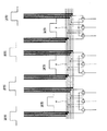
また、時分割駆動を実現するために、n列分の信号ライン12-1〜12-nを時分割数に対応した本数(本例では、3時分割に対応して3本)を1単位(ブロック)として分割した場合において、水平駆動回路22は、図1から明らかなように、その分割した数kに対応したk個のドライバIC、例えばTAB(Tape Automated Bonding)IC(1) 28-1〜TABIC(k) 28-kによって構成されている。
Further, in order to realize time division driving, the number of signal lines 12-1 to 12-n for n columns corresponding to the number of time divisions (in this example, three corresponding to three time divisions) is one unit. When divided as (block), the
そして、これらTABIC(1) 28-1〜TABIC(k) 28-kは、液晶表示パネル14の基板とは別体の外部回路基板29-1〜29-k上に搭載され、1分割ブロック内の複数本の信号ラインに与える信号電位を時系列で出力するようになっている。これに対応して、k個の時分割スイッチ30-1〜30-kが、n列分の信号ライン12-1〜12-nの入力段に設けられている。 These TABIC (1) 28-1 to TABIC (k) 28-k are mounted on external circuit boards 29-1 to 29-k that are separate from the substrate of the liquid crystal display panel 14, and are included in one divided block. The signal potentials applied to the plurality of signal lines are output in time series. Correspondingly, k time-division switches 30-1 to 30-k are provided at the input stage of the signal lines 12-1 to 12-n for n columns.
時分割スイッチ30-1は3時分割を実現するために、特に図2から明らかなように、PchMOSトランジスタおよびNMOSトランジスタが並列に接続されてなる3個のCMOSアナログスイッチ(トランスミッションスイッチ)31,32,33からなり、液晶表示パネル14と同一基板上に薄膜トランジスタによって形成されている。他の時分割スイッチ30-2〜30-kについても、時分割スイッチ30-1と全く同じ構成となっている。 In order to realize the three time division, the time division switch 30-1 has three CMOS analog switches (transmission switches) 31, 32 in which a PchMOS transistor and an NMOS transistor are connected in parallel, as is apparent from FIG. , 33 and formed on the same substrate as the liquid crystal display panel 14 by thin film transistors. The other time division switches 30-2 to 30-k have the same configuration as the time division switch 30-1.
そして、例えば時分割スイッチ30-1において、3個のアナログスイッチ31,32,33の各入力端は共通に接続され、その共通接続点は共通信号ライン34-1を介してTABIC28-1の出力端に接続されている。これにより、TABIC(1) 28-1から時系列で出力される信号電位が、共通信号ライン34-1を経由して3個のアナログスイッチ31,32,33の各入力端に与えられる。これらアナログスイッチ31,32,33の各出力端は、3本の信号ライン12-1,12-2,12-3の各一端に接続されている。
For example, in the time division switch 30-1, the input terminals of the three
時分割スイッチ30-2に対しては、共通信号ライン34-2を経由してTABIC(2) 28-2から時系列の信号電位が供給される。同様にして、時分割スイッチ30-kに対しては、共通信号ライン34-kを経由してTABIC(k) 28-kから時系列の信号電位が供給される。なお、本例では、簡単のため、1個のTABICにつき1本の共通信号ラインを配した構成を示したが、実際には複数本の共通信号ラインが配されることになる。 A time-series signal potential is supplied from the TABIC (2) 28-2 to the time division switch 30-2 via the common signal line 34-2. Similarly, a time-series signal potential is supplied from the TABIC (k) 28-k to the time division switch 30-k via the common signal line 34-k. In this example, for the sake of simplicity, a configuration in which one common signal line is provided for each TABIC is shown. However, in practice, a plurality of common signal lines are provided.
また、液晶表示パネル14と同一基板上において、1個のアナログスイッチにつき2本、計6本の制御ライン35-1〜35-6が、ゲートライン11-1〜11-mの配線方向に沿って配線されている。そして、例えば時分割スイッチ30-1にあっては、アナログスイッチ31の2つの制御入力端(即ち、Nch,PchMOSトランジスタの各ゲート)が制御ライン35-1,35-2に、アナログスイッチ32の2つの制御入力端が制御ライン35-3,35-4に、アナログスイッチ33の2つの制御入力端が制御ライン35-5,35-6にそれぞれ接続されている。
On the same substrate as the liquid crystal display panel 14, two control lines 35-1 to 35-6, two for each analog switch, are provided along the wiring direction of the gate lines 11-1 to 11-m. Are wired. For example, in the time division switch 30-1, the two control input terminals (that is, the gates of the Nch and PchMOS transistors) of the
なお、ここでは、時分割スイッチ30-1の3個のアナログスイッチ31〜33の6本の制御ライン35-1〜35-6に対する接続関係について説明したが、他の時分割スイッチ30-2〜30-kについても全く同じ接続関係となっている。
Here, the connection relation of the three
6本の制御ライン35-1〜35-6には、時分割スイッチ30-1〜30-kの各3個のアナログスイッチ31〜33を選択するための制御信号S1〜S3,XS1〜XS3を外部から与える必要がある。ただし、制御信号XS1〜XS3は、制御信号S1〜S3の反転信号である。この制御信号S1〜S3,XS1〜XS3は、TABIC28-1〜28-kの各々から出力される時系列の信号電位に同期して、時分割スイッチ30-1〜30-kの各3個のアナログスイッチ31〜33を順次オンさせるための信号である。
Control signals S1 to S3 and XS1 to XS3 for selecting each of the three
この制御信号S1〜S3,XS1〜XS3の液晶表示パネル14への入力は、水平駆動回路22側から、即ち液晶表示パネル14の上側から複数の個所にて行われる。具体的には、k個の時分割スイッチ30-1〜30-kごとに6本の制御ライン36-1〜36-6が、TABIC28-1〜28-kをそれぞれ搭載した外部回路基板29-1〜29-kを通して、液晶表示パネル14上の6本の制御ライン35-1〜35-6まで配線される。
The control signals S1 to S3, XS1 to XS3 are inputted to the liquid crystal display panel 14 from the
この制御ライン36-1〜36-6の配線は、例えば、TABの低膨張のテープを用いて行われる。そして、6本の制御ライン36-1〜36-6のうち、制御ライン36-1は制御信号S1を、制御ライン36-2は制御信号XS1を、制御ライン36-3は制御信号S2を、制御ライン36-4は制御信号XS2を、制御ライン36-5は制御信号S3を、制御ライン36-6は制御信号XS3をそれぞれ伝送することになる。
The control lines 36-1 to 36-6 are wired using, for example, a TAB low expansion tape. Of the six control lines 36-1 to 36-6, the control line 36-1 is the
図5は、液晶表示パネル14の基板上に形成される薄膜トランジスタの断面構造図である。同図において、(a)はボトムゲート構造の薄膜トランジスタを、(b)はトップゲート構造の薄膜トランジスタをそれぞれ示している。 FIG. 5 is a cross-sectional structure diagram of a thin film transistor formed on the substrate of the liquid crystal display panel 14. In the figure, (a) shows a thin film transistor with a bottom gate structure, and (b) shows a thin film transistor with a top gate structure.
図5(a)に示すボトムゲート構造の薄膜トランジスタでは、ガラス基板41の上にゲート電極42が形成され、その上にゲート絶縁膜43を介してポリシリコン(Poly−Si)層44が形成され、さらにその上に層間絶縁膜45が形成されている。また、ゲート電極42の側方のゲート絶縁膜43上には、N+ 拡散層からなるソース領域46およびドレイン領域47が形成され、これらの領域46,47にはソース電極48およびドレイン電極49がそれぞれ接続されている。
In the bottom gate thin film transistor shown in FIG. 5A, a gate electrode 42 is formed on a glass substrate 41, and a polysilicon (Poly-Si)
図5(b)に示すトップゲート構造の薄膜トランジスタでは、ガラス基板51の上にポリシリコン層52が形成され、その上にゲート絶縁膜53を介してゲート電極54が形成され、さらにその上に層間絶縁膜55が形成されている。また、ポリシリコン層52の側方のガラス基板51上には、N+ 拡散層からなるソース領域56およびドレイン領域57が形成され、これらの領域56,57にはソース電極58およびドレイン電極59がそれぞれ接続されている。
In the thin film transistor having the top gate structure shown in FIG. 5B, a
次に、上記構成における時分割スイッチ30-1,30-2,30-3の動作について、図6のタイミングチャートを用いて説明する。なお、図1には、時分割スイッチ30-3およびこれに対応するTABIC(3) については省略されている。 Next, the operation of the time division switches 30-1, 30-2, 30-3 in the above configuration will be described with reference to the timing chart of FIG. In FIG. 1, the time division switch 30-3 and the corresponding TABIC (3) are omitted.
また、本例では、R(赤),G(緑),B(青)に対応した3分割(時分割)駆動への適用の場合を例に採っていることから、TABIC(1) 28-1,TABIC(2) 28-2,TABIC(3) 28-3からは、R,G,Bの3画素分の信号電位が順に時系列で出力され、共通信号ライン34-1,34-2,34-3によって時分割スイッチ30-1,30-2,30-3へ伝送される。 Further, in this example, since the case of application to three-division (time division) driving corresponding to R (red), G (green), and B (blue) is taken as an example, TABIC (1) 28- 1, TABIC (2) 28-2 and TABIC (3) 28-3 output signal potentials for three pixels of R, G, and B in order in time series, and common signal lines 34-1 and 34-2. , 34-3 to the time division switches 30-1, 30-2, 30-3.
具体的には、図6のタイミングチャートに示すように、TABIC(1) 28-1から時分割スイッチ30-1にはR1,G1,B1の各画素の信号電位が、TABIC(2) 28-2から時分割スイッチ30-2にはR2,G2,B2の各画素の信号電位が、TABIC(3) 28-3から時分割スイッチ30-3にはR3,G3,B3の各画素の信号電位が、……という具合に伝送される。 Specifically, as shown in the timing chart of FIG. 6, the signal potential of each pixel of R1, G1, and B1 from TABIC (1) 28-1 to time division switch 30-1 is TABIC (2) 28-. 2 to the time division switch 30-2, the signal potentials of the R2, G2, and B2 pixels, and the TABIC (3) 28-3 to the time division switch 30-3, the signal potentials of the R3, G3, and B3 pixels. But ...
一方、時分割スイッチ30-1,30-2,30-3には、上記の時系列の信号に同期した制御信号S1,XS1,S2,XS2,S3,XS3が、外部回路基板29-1〜29-kを通して配線された6本の制御ライン36-1〜36-6および液晶表示パネル14の基板上に配線された6本の制御ライン35-1〜35-6を経由して与えられる。 On the other hand, control signals S1, XS1, S2, XS2, S3, and XS3 synchronized with the time-series signals are supplied to the time division switches 30-1, 30-2, and 30-3 from the external circuit boards 29-1 to 29-3. The six control lines 36-1 to 36-6 wired through 29-k and the six control lines 35-1 to 35-6 wired on the substrate of the liquid crystal display panel 14 are given.
これにより、制御信号S1が“H”レベルのときは、アナログスイッチ31がオン状態となり、R1,R3の各画素の信号電位を信号ライン12-1〜12-nの対応する信号ラインにそれぞれ与える。制御信号S2が“H”レベルのときは、アナログスイッチ32がオン状態となり、G2の画素の信号電位を信号ライン12-1〜12-nの対応する信号ラインに与える。制御信号S3が“H”レベルのときは、アナログスイッチ33がオン状態となり、B1,B3の各画素の信号電位を信号ライン12-1〜12-nの対応する信号ラインにそれぞれ与える。
As a result, when the control signal S1 is at "H" level, the
上述したように、各画素に行単位で順に信号電位を与えるための水平駆動回路22を、液晶表示パネル14の外部回路として設けてなるアクティブマトリクス型液晶表示装置において、時分割スイッチ30-1〜30-kに制御信号S1,XS1,S2,XS2,S3,XS3を外部から伝送する制御ライン36-1〜36-6を、液晶表示パネル14の上側に配された外部回路基板29-1〜29-kを通して配線したことにより、液晶表示パネル14の左右両側にフレキシブルケーブルを接続する場合に比べて液晶表示パネル14の左右の額縁サイズを縮小できることになる。
As described above, in the active matrix liquid crystal display device in which the
特に、制御ライン36-1〜36-6を、外部回路基板29-1〜29-k上に搭載されたTABIC(1) 28-1〜TABIC(k) 28-kのテープを用いて配線するようにしたことにより、TABの接続工程で制御ライン36-1〜36-6の接続も同時に行える。したがって、フレキシブルケーブルを用いる場合のその接続工程が不要となるため、工程数を1つ削減でき、その分だけ製造コストを低減できることにもなる。 In particular, the control lines 36-1 to 36-6 are wired using a tape of TABIC (1) 28-1 to TABIC (k) 28-k mounted on the external circuit boards 29-1 to 29-k. By doing so, the control lines 36-1 to 36-6 can be simultaneously connected in the TAB connection step. Therefore, since the connection process in the case of using a flexible cable becomes unnecessary, the number of processes can be reduced by one, and the manufacturing cost can be reduced correspondingly.
また、制御ライン36-1〜36-6を外部回路基板29-1〜29-kの各々を通して配線し、液晶表示パネル14の基板上に配線された制御ライン35-1〜35-6に対して制御信号S1,XS1,S2,XS2,S3,XS3を複数の個所から入力するようにしたことにより、制御ライン35-1〜35-6の実質的な配線抵抗を小さくすることができる。 Also, control lines 36-1 to 36-6 are wired through the external circuit boards 29-1 to 29-k, and are connected to the control lines 35-1 to 35-6 wired on the substrate of the liquid crystal display panel 14. Thus, since the control signals S1, XS1, S2, XS2, S3, and XS3 are input from a plurality of locations, the substantial wiring resistance of the control lines 35-1 to 35-6 can be reduced.
しかも、外側のTABを用いて配線された制御ライン36-1〜36-6の配線幅は、液晶表示パネル14の基板上に配線された制御ライン35-1〜35-6の配線幅(例えば、7μm)よりも大きく(例えば、100μm)、かつ配線材料はアルミニウムに対して比抵抗の小さい銅を使用しているため、配線抵抗を格段に小さくすることができる。 Moreover, the wiring widths of the control lines 36-1 to 36-6 wired using the outer TAB are the wiring widths of the control lines 35-1 to 35-6 wired on the substrate of the liquid crystal display panel 14 (for example, , 7 μm) (for example, 100 μm), and the wiring material uses copper having a small specific resistance with respect to aluminum, so that the wiring resistance can be remarkably reduced.
このように、制御信号S1,XS1,S2,XS2,S3,XS3を伝送する制御ライン36-1〜36-6および制御ライン35-1〜35-6の配線抵抗を小さくできることにより、図7に示すように、これらの配線抵抗による時定数を小さくできるため、この時定数に起因する制御信号S1,XS1,S2,XS2,S3,XS3の遅延を抑えることができる。 As described above, the wiring resistance of the control lines 36-1 to 36-6 and the control lines 35-1 to 35-6 that transmit the control signals S1, XS1, S2, XS2, S3, and XS3 can be reduced. As shown, since the time constants due to these wiring resistances can be reduced, the delay of the control signals S1, XS1, S2, XS2, S3, and XS3 due to the time constants can be suppressed.
これにより、この遅延に起因する画質の低下を未然に防止できるとともに、制御信号S1,XS1,S2,XS2,S3,XS3の時間的マージン(図6に示すα)を十分に確保でき、ブランキング期間を小さくすることができるため、ドット周波数の増大による液晶の高速駆動が実現でき、14インチ以上のXGA、SXGA、UXGAもしくは4インチ以上のVGA、SVGAに対応可能な液晶表示装置を作製できる。 As a result, it is possible to prevent the image quality from being deteriorated due to this delay, and to sufficiently secure the time margin (α shown in FIG. 6) of the control signals S1, XS1, S2, XS2, S3, and XS3. Since the period can be shortened, high-speed liquid crystal driving can be realized by increasing the dot frequency, and a liquid crystal display device compatible with XGA, SXGA, UXGA of 14 inches or more, or VGA or SVGA of 4 inches or more can be manufactured.
なお、上記実施形態においては、信号ライン12-1〜12-nを駆動する水平駆動回路22を、液晶表示パネル14の一方側(本例では、上側)に配置した構成の液晶表示装置に適用した場合について説明したが、水平駆動回路22を例えばコモン電圧Vcomを基準に2つに分割し、この2つの水平駆動回路を液晶表示パネル14の上下に配置した構成の液晶表示装置についても同様に適用することが可能である。
In the above embodiment, the
11-1〜11-m…ゲートライン、12-1〜12-n…信号ライン、13…単位画素、14…液晶表示パネル、15…薄膜トランジスタ、16…付加容量、17…液晶容量、18…垂直駆動回路、22…水平駆動回路、28-1〜28-k…TABIC(1) 〜TABIC(k) 、29-1〜29-k…外部回路基板、30-1〜30-k…時分割スイッチ、31〜33…アナログスイッチ、34-1〜34-k…共通信号ライン、35-1〜35-k,36-1〜36-k…制御ライン 11-1 to 11-m: gate lines, 12-1 to 12-n: signal lines, 13: unit pixels, 14: liquid crystal display panels, 15: thin film transistors, 16: additional capacitors, 17: liquid crystal capacitors, 18: vertical Drive circuit, 22 ... Horizontal drive circuit, 28-1 to 28-k ... TABIC (1) to TABIC (k), 29-1 to 29-k ... External circuit board, 30-1 to 30-k ... Time division switch 31-33 ... Analog switch, 34-1 to 34-k ... Common signal line, 35-1 to 35-k, 36-1 to 36-k ... Control line
Claims (1)
前記基板上に設けられ、前記複数行分のゲートラインを駆動する垂直駆動回路と、
前記複数列分の信号ラインを時分割数に対応した本数を単位とするとき、当該本数の信号ラインの各々に対応して前記基板上に設けられ、入力される時系列の信号電圧を対応する信号ラインの各々に時分割にて供給する時分割数分のスイッチ素子から成る複数個の時分割スイッチと、
前記複数個の時分割スイッチの各々に対して前記時系列の信号電圧を供給する複数個の集積回路から成る水平駆動回路と、
前記複数個の集積回路の各々を搭載する複数個の回路基板から成る外部回路基板と、
前記ゲートラインの配線方向に沿って前記基板に配線された第1の制御ラインと、
前記複数個の回路基板の各々を通して前記第1の制御ラインまで配線され、当該第1の制御ラインを通して前記複数個のスイッチ素子に対してその選択のための制御信号を伝送する第2の制御ラインとを備え、
前記第1の制御ラインに対して前記制御信号を前記第2の制御ラインによって複数の個所から入力する
液晶表示装置。 A display unit in which pixels are formed at intersections of a plurality of rows of gate lines and a plurality of columns of signal lines wired in a matrix on the substrate;
Provided on the substrate, a vertical driving circuit for driving the gate lines of the plurality rows,
When the number of signal lines corresponding to the plurality of columns is a unit corresponding to the number of time divisions , the time series signal voltages provided on the substrate corresponding to each of the number of signal lines and corresponding to the number of signal lines. A plurality of time-division switches composed of the number of time-division switch elements supplied to each of the signal lines in a time-division manner;
A horizontal drive circuit comprising a plurality of integrated circuits for supplying the time series signal voltage to each of the plurality of time division switches ;
An external circuit board comprising a plurality of circuit boards on which each of the plurality of integrated circuits is mounted;
First control lines wired in the substrate along the wiring direction of the gate line,
Wherein through each of the plurality of circuit board to said first control line is wired, the second control line for transmitting control signals for that selected for the plurality of switching elements through the first control line And
The liquid crystal display device for inputting a plurality of positions by said control signal to said first control line and the second control line.
Priority Applications (1)
| Application Number | Priority Date | Filing Date | Title |
|---|---|---|---|
| JP2007263260A JP4760812B2 (en) | 2007-10-09 | 2007-10-09 | Liquid crystal display |
Applications Claiming Priority (1)
| Application Number | Priority Date | Filing Date | Title |
|---|---|---|---|
| JP2007263260A JP4760812B2 (en) | 2007-10-09 | 2007-10-09 | Liquid crystal display |
Related Parent Applications (1)
| Application Number | Title | Priority Date | Filing Date |
|---|---|---|---|
| JP10200130A Division JP2000029441A (en) | 1998-07-15 | 1998-07-15 | Liquid crystal display device |
Publications (3)
| Publication Number | Publication Date |
|---|---|
| JP2008097005A JP2008097005A (en) | 2008-04-24 |
| JP2008097005A5 JP2008097005A5 (en) | 2010-01-21 |
| JP4760812B2 true JP4760812B2 (en) | 2011-08-31 |
Family
ID=39379841
Family Applications (1)
| Application Number | Title | Priority Date | Filing Date |
|---|---|---|---|
| JP2007263260A Expired - Fee Related JP4760812B2 (en) | 2007-10-09 | 2007-10-09 | Liquid crystal display |
Country Status (1)
| Country | Link |
|---|---|
| JP (1) | JP4760812B2 (en) |
Families Citing this family (4)
| Publication number | Priority date | Publication date | Assignee | Title |
|---|---|---|---|---|
| US8593210B2 (en) | 2009-02-17 | 2013-11-26 | Sharp Kabushiki Kaisha | Signal distribution device and display device |
| CN102792450B (en) | 2010-03-24 | 2014-02-26 | 夏普株式会社 | Signal distribution circuit, signal distribution device, and display device |
| JP2012132973A (en) * | 2010-12-20 | 2012-07-12 | Seiko Epson Corp | Driving device and electronic apparatus using driving device |
| WO2014080828A1 (en) | 2012-11-22 | 2014-05-30 | シャープ株式会社 | Display device and electronic device |
Citations (4)
| Publication number | Priority date | Publication date | Assignee | Title |
|---|---|---|---|---|
| JPH0452684A (en) * | 1990-06-20 | 1992-02-20 | Nec Kansai Ltd | Driving method of liquid crystal display panel |
| JPH0667200A (en) * | 1992-08-17 | 1994-03-11 | Toshiba Corp | Liquid crystal display device |
| JPH07181511A (en) * | 1993-12-22 | 1995-07-21 | Nec Corp | Liquid crystal display device |
| JPH08227068A (en) * | 1995-11-28 | 1996-09-03 | Seiko Epson Corp | Liquid crystal display device |
-
2007
- 2007-10-09 JP JP2007263260A patent/JP4760812B2/en not_active Expired - Fee Related
Patent Citations (4)
| Publication number | Priority date | Publication date | Assignee | Title |
|---|---|---|---|---|
| JPH0452684A (en) * | 1990-06-20 | 1992-02-20 | Nec Kansai Ltd | Driving method of liquid crystal display panel |
| JPH0667200A (en) * | 1992-08-17 | 1994-03-11 | Toshiba Corp | Liquid crystal display device |
| JPH07181511A (en) * | 1993-12-22 | 1995-07-21 | Nec Corp | Liquid crystal display device |
| JPH08227068A (en) * | 1995-11-28 | 1996-09-03 | Seiko Epson Corp | Liquid crystal display device |
Also Published As
| Publication number | Publication date |
|---|---|
| JP2008097005A (en) | 2008-04-24 |
Similar Documents
| Publication | Publication Date | Title |
|---|---|---|
| US10699627B2 (en) | Driving method of display panel, display panel and display device | |
| US8471981B2 (en) | Display apparatus and display set having the same | |
| US7088328B2 (en) | Liquid crystal display device having a circuit for controlling polarity of video signal for each pixel | |
| EP2043084B1 (en) | Electro-optical device and electronic apparatus | |
| JP2008225142A (en) | Electrooptical device, driving circuit, and electronic equipment | |
| JP2002072233A (en) | Liquid crystal display apparatus and portable terminal | |
| KR20090110095A (en) | Display apparatus | |
| JP4256717B2 (en) | Liquid crystal drive device and liquid crystal display device | |
| JP2008058762A (en) | Electrooptical device, driving circuit, and electronic equipment | |
| JP2005257710A (en) | Display apparatus | |
| US20090184913A1 (en) | Display device and electronic apparatus | |
| JP4760812B2 (en) | Liquid crystal display | |
| JP2000029441A (en) | Liquid crystal display device | |
| US7420537B2 (en) | Liquid crystal display and dummy loading device thereof | |
| JP4702114B2 (en) | Demultiplexer, electro-optical device and electronic apparatus | |
| JP4385967B2 (en) | Electro-optical device drive circuit, electro-optical device including the same, and electronic apparatus | |
| KR20080040448A (en) | Liquid crystal display device and gate driving circuit thereof | |
| JP2005195810A (en) | Capacitive load drive circuit and display panel drive circuit | |
| KR100571032B1 (en) | Liquid crystal display | |
| TWI382263B (en) | Liquid crystal display of the double gate electrode crystal substrate | |
| JP2001324963A (en) | Display device | |
| JP3251391B2 (en) | Image display device | |
| JP2006201315A (en) | Liquid crystal display device | |
| JP4302816B2 (en) | Liquid crystal display | |
| JP4602385B2 (en) | Liquid crystal display |
Legal Events
| Date | Code | Title | Description |
|---|---|---|---|
| A521 | Written amendment |
Free format text: JAPANESE INTERMEDIATE CODE: A821 Effective date: 20091014 |
|
| RD02 | Notification of acceptance of power of attorney |
Free format text: JAPANESE INTERMEDIATE CODE: A7422 Effective date: 20091014 |
|
| RD04 | Notification of resignation of power of attorney |
Free format text: JAPANESE INTERMEDIATE CODE: A7424 Effective date: 20091030 |
|
| A521 | Written amendment |
Free format text: JAPANESE INTERMEDIATE CODE: A523 Effective date: 20091130 |
|
| A977 | Report on retrieval |
Free format text: JAPANESE INTERMEDIATE CODE: A971007 Effective date: 20101207 |
|
| A131 | Notification of reasons for refusal |
Free format text: JAPANESE INTERMEDIATE CODE: A131 Effective date: 20101221 |
|
| A521 | Written amendment |
Free format text: JAPANESE INTERMEDIATE CODE: A523 Effective date: 20110127 |
|
| A131 | Notification of reasons for refusal |
Free format text: JAPANESE INTERMEDIATE CODE: A131 Effective date: 20110301 |
|
| A521 | Written amendment |
Free format text: JAPANESE INTERMEDIATE CODE: A523 Effective date: 20110404 |
|
| A01 | Written decision to grant a patent or to grant a registration (utility model) |
Free format text: JAPANESE INTERMEDIATE CODE: A01 Effective date: 20110510 |
|
| A61 | First payment of annual fees (during grant procedure) |
Free format text: JAPANESE INTERMEDIATE CODE: A61 Effective date: 20110523 |
|
| FPAY | Renewal fee payment (event date is renewal date of database) |
Free format text: PAYMENT UNTIL: 20140617 Year of fee payment: 3 |
|
| FPAY | Renewal fee payment (event date is renewal date of database) |
Free format text: PAYMENT UNTIL: 20140617 Year of fee payment: 3 |
|
| FPAY | Renewal fee payment (event date is renewal date of database) |
Free format text: PAYMENT UNTIL: 20140617 Year of fee payment: 3 |
|
| S111 | Request for change of ownership or part of ownership |
Free format text: JAPANESE INTERMEDIATE CODE: R313113 |
|
| FPAY | Renewal fee payment (event date is renewal date of database) |
Free format text: PAYMENT UNTIL: 20140617 Year of fee payment: 3 |
|
| R350 | Written notification of registration of transfer |
Free format text: JAPANESE INTERMEDIATE CODE: R350 |
|
| R250 | Receipt of annual fees |
Free format text: JAPANESE INTERMEDIATE CODE: R250 |
|
| R250 | Receipt of annual fees |
Free format text: JAPANESE INTERMEDIATE CODE: R250 |
|
| R250 | Receipt of annual fees |
Free format text: JAPANESE INTERMEDIATE CODE: R250 |
|
| R250 | Receipt of annual fees |
Free format text: JAPANESE INTERMEDIATE CODE: R250 |
|
| LAPS | Cancellation because of no payment of annual fees |