JP4754677B2 - Method for manufacturing semiconductor device - Google Patents
Method for manufacturing semiconductor device Download PDFInfo
- Publication number
- JP4754677B2 JP4754677B2 JP2000232528A JP2000232528A JP4754677B2 JP 4754677 B2 JP4754677 B2 JP 4754677B2 JP 2000232528 A JP2000232528 A JP 2000232528A JP 2000232528 A JP2000232528 A JP 2000232528A JP 4754677 B2 JP4754677 B2 JP 4754677B2
- Authority
- JP
- Japan
- Prior art keywords
- substrate
- semiconductor device
- manufacturing
- film
- region
- Prior art date
- Legal status (The legal status is an assumption and is not a legal conclusion. Google has not performed a legal analysis and makes no representation as to the accuracy of the status listed.)
- Expired - Fee Related
Links
Images


Landscapes
- Devices For Indicating Variable Information By Combining Individual Elements (AREA)
- Liquid Crystal (AREA)
- Transforming Electric Information Into Light Information (AREA)
- Thin Film Transistor (AREA)
Description
【0001】
【発明の属する技術分野】
本願発明は薄膜トランジスタ(以下、TFTという)で構成された回路を有する半導体装置およびその作製方法に関する。例えば、液晶表示パネルに代表される電気光学装置およびその様な電気光学装置を部品として搭載した電子機器に関する。
【0002】
なお、本明細書中において半導体装置とは、半導体特性を利用することで機能しうる装置全般を指し、電気光学装置、半導体回路および電子機器は全て半導体装置である。
【0003】
【従来の技術】
近年、絶縁表面を有する基板上に形成された半導体薄膜(厚さ数〜数百nm程度)を用いて薄膜トランジスタ(TFT)を構成する技術が注目されている。薄膜トランジスタはICや電気光学装置のような電子デバイスに広く応用され、特に画像表示装置のスイッチング素子として開発が急がれている。
【0004】
このような画像表示装置を利用したアプリケーションは様々なものが期待されているが、特に携帯機器への利用が注目されている。そのため、フレキシブルなプラスチックフィルムの上にTFT素子を形成することが試みられている。
【0005】
しかしながら、プラスチックフィルムの耐熱性が低いためプロセスの最高温度を低くせざるを得ず、結果的にガラス基板上に形成する時ほど良好な電気特性のTFTを形成できないのが現状である。そのため、プラスチックフィルムを用いた高性能な液晶表示装置は実現されていない。
【0006】
【発明が解決しようとする課題】
本発明は、上記問題点を鑑みてなされたものであり、本発明は、フレキシブルなフィルム上に発光素子を形成して軽量化して安価な電気光学装置を提供することを課題とする。さらに、それを表示部として有する安価な電気器具を提供することを課題とする。
【0007】
【課題を解決するための手段】
本発明は、素子形成基板としてプラスチック基板を用いるのではなく、厚さの薄い金属基板を用い、フレキシブルな金属基板上に必要な素子を形成して軽量化した電気光学装置を得ることを特徴としている。
【0008】
なお、前記必要な素子とは、アクティブマトリクス型の電気光学装置ならば画素のスイッチング素子として用いる半導体素子(典型的にはTFT)もしくはMIM素子を指す。
【0009】
本明細書で開示する発明の構成は、
金属表面を有する基板上に絶縁膜と、該絶縁膜上に駆動回路と画素部と、対向基板と、該対向基板と前記金属表面を有する基板との間に液晶材料と、を有することを特徴とする半導体装置である。
【0010】
上記構成において、前記金属表面を有する基板は、ステンレス基板であることを特徴としている。
【0011】
また、上記構成において、前記ステンレス基板の厚さは10μm〜30μmであることを特徴としている。
【0012】
また、上記構成において、前記金属表面を有する基板の表面粗さは、1μmRMAX以下であることを特徴としている。
【0013】
また、上記構成において、前記金属表面を有する基板の表面に存在する凸部の曲率半径は、1μm以上であることを特徴としている。
【0014】
また、上記構成において、半導体装置とは、反射型の液晶表示装置であることを特徴としている。
【0015】
また、上記構造を実現するため、本発明は、薄い金属基板の端部を曲げて、端部に曲率を持っている基板ホルダーに密着性よく真空中で固定した後、薄い金属基板上に必要な素子を形成し、該素子上に固定基板を接着層(シール材等)で貼り合わせた後に液晶材料を封止保持した後、基板ホルダーを分離することを特徴としている。
【0016】
また、上記構造を実現するための発明の構成は、
金属表面を有する基板の端部を曲げて基板ホルダーに固定する工程と、
前記金属表面を有する基板上に絶縁膜を形成する工程と、
前記絶縁膜の上にTFT素子及び画素電極を形成する工程と、
前記画素電極の上に接着層で固定基板を貼り合わせる工程と、
前記基板基板ホルダーを分離する工程と、
を有することを特徴とする半導体装置である。
【0017】
また、上記構成において、前記固定する工程は真空中で行うことを特徴としている。
【0018】
また、上記構成において、前記固定する工程は室温〜400℃で行うことを特徴としている。
【0019】
また、上記構成において、前記基板基板ホルダーの端部は曲面を有していることを特徴としている。
【0020】
また、上記構成において、前記基板基板ホルダーは、前記金属表面を有する基板と同じ熱膨張係数を有することを特徴としている。
【0021】
また、上記構成において、前記金属表面を有する基板は、ステンレス基板であることを特徴としている。また、前記ステンレス基板の厚さは10μm〜30μmであることを特徴としている。
【0022】
また、上記構成において、前記基板基板ホルダーは、ステンレス基板であることを特徴としている。また、前記ステンレス基板の厚さは500μm〜1000μmであることを特徴としている。
【0023】
また、上記構成において、前記画素電極と前記固定基板との間に液晶材料を備えることを特徴としている。
【0024】
また、上記構成に記載された半導体装置とは、反射型の液晶表示装置であることを特徴としている。
【0025】
なお、本明細書中でのステンレスとは、クロムを約12%以上含有する鋼(鉄と炭素の合金)を指しており、組成上、マルテンサイト系やフェライト系やオーステナイト系に大別できる。なお、Ti、Nb、Mo、Cu、Ni、またはSiから選ばれた一種または複数種を添加したステンレス鋼をも含む。
【0026】
【発明の実施の形態】
本願発明の実施形態について、以下に説明する。
【0027】
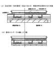
まず、素子形成基板となる金属基板102と、基板ホルダー101とを用意する。金属基板102(金属表面を有する基板)としては、ステンレス基板を用意する。この基板102の厚さは10μm〜30μmのものを用いる。また、基板ホルダー101としては、金属基板102よりも厚いステンレス基板を用意する。この基板101の厚さは500μm〜1000μmのものを用いる。また、基板ホルダー101としては、セラミックあるいはAl2O3を用いることもできる。
【0028】
次いで、図1(A)に示すように端部に少なくとも曲面を持つ基板ホルダー101と金属基板102とを間に空気が入らないように固定し、さらに固定部103を用いて金属基板102の端部を固定し、密着性をより強固なものとする。こうして、固定した状態を図1(B)に示した。ここでは、固定部103を枠とし、基板ホルダー101をはめ込むようにして接着材を用いることなく金属基板102を基板ホルダー101に固定した。また、固定部をテープ状またはバンド状として金属基板の端部を基板ホルダーに固定してもよい。なお、金属基板102を基板ホルダー101に密着させて固定する工程は、室温〜400℃、かつ真空中で行うことによって、両基板間に空気が入らないようにすることが好ましい。また、金属基板102に広げる力を加えながら基板ホルダーに被せ、必要があれば押し付けることで密着させてもよい。
【0029】
また、固定後の金属基板における表面の凹凸の表面粗さは、1μmRMAX以下と平坦なものとすることが好ましい。あるいは、固定後の金属基板における表面の凹凸の1mm平方当りの表面粗さが1μmとなることが好ましい。さらに、その凹凸の凸部の曲率半径は、1μm以上、好ましくは10μm以上とする。また、金属基板における表面の平坦性を向上させる公知の技術、例えばCMP(ケミカルメカニカルポリッシング)と呼ばれる研磨工程を用いてもよい。
【0030】
次いで、金属基板102上に下地絶縁膜を形成した後、その下地絶縁膜上に必要な素子を形成する。なお、簡略化のため下地絶縁膜の表面を平坦なものとして示しているが、実際には固定部と金属基板とが接触する部分に段差が生じる。素子形成基板がプラスチック基板であればプロセス温度が350℃以下とする必要があったが、本発明は、素子形成基板が金属基板であるので350℃以上の熱処理が可能である。なお、この素子形成工程の熱処理によって基板同士が分離しないように、基板ホルダーと金属基板との熱膨張係数を一致させることが好ましい。ここでは、駆動回路104とTFT素子を有する画素部105を形成した例を示す。(図1(C))
【0031】
次いで、固定基板106を接着層(シール材)107で貼り合わせる。(図2(A))なお、ここでは液晶材料108を保持するために固定基板106を用いたが、特に必要がなければ用いなくともよい。固定基板106としては、透光性を有する樹脂基板またはガラス基板を用いればよく、片面もしくは両面に保護膜としてDLC膜を設けたものを用いてもよい。
【0032】
次いで、基板間に液晶材料108を注入した後、注入口を封止する。
【0033】
次いで、裏面側から物理的手段、例えば、固定部103を除去することによって基板ホルダーを除去する。特に接着材を用いていないので分離しやすい。基板ホルダーと金属基板との間に対して流体(圧力が加えられた液体もしくは気体)を噴射することにより基板ホルダーを分離する方法を用いてもよい。ここでは、基板ホルダー及び金属基板の端部を切断することによって、基板ホルダーと金属基板を分離する。(図2(B))
【0034】
そして、最終的には、薄い金属基板108である素子形成基板と樹脂基板である固定基板とで挟まれた液晶表示装置が完成する。なお、この液晶表示装置は反射型であり、画素部のTFT素子に接続される画素電極は反射性の高い材料で形成されている。
【0035】
なお、図1及び図2では、簡略化のために基板ホルダーの端部とTFT素子とをあまり離さずに図示したが、実際には十分距離を離したほうが好ましい。
【0036】
以上の構成でなる本願発明について、以下に示す実施例でもってさらに詳細な説明を行うこととする。
【0037】
【実施例】
[実施例1]
本実施例は、薄い金属基板である素子形成基板と樹脂基板である固定基板とで挟まれた液晶表示装置の作製方法の一例を図1及び図2を用いて示す。ただし、本発明が本実施例に限定されないことはいうまでもない。
【0038】
まず、基板ホルダー101としてステンレス基板を用いる。そして、上記実施の形態に示した方法を用いて、基板ホルダー101と薄い金属基板である素子形成基板102とを固定部103で固定した。(図1(B))
【0039】
次いで、金属基板102上に下地絶縁膜を形成した後、その下地絶縁膜上に必要な素子を形成する。ここでは、駆動回路104とTFT素子を有する画素部105を形成した例を示す。(図1(C))
【0040】
下地絶縁膜としては、酸化シリコン膜、窒化シリコン膜、窒化酸化シリコン膜(SiOx Ny )、またはこれらの積層膜等を100〜500nmの膜厚範囲で用いることができ、形成手段としては公知の成膜方法(熱CVD法、プラズマCVD法、蒸着法、スパッタ法、減圧熱CVD法等)を用いる。ここでは、膜組成において酸素元素より窒素元素を多く含む酸化窒化シリコン膜と、膜組成において窒素元素より酸素元素を多く含む酸化窒化シリコン膜を積層形成した。
【0041】
次いで、下地絶縁膜上に半導体層を形成する。半導体層の材料に限定はないが、好ましくはシリコンまたはシリコンゲルマニウム(SiXGe1-X(0<X<1))合金などで形成すると良い。形成手段としては公知の成膜方法(熱CVD法、プラズマCVD法、蒸着法、スパッタ法、減圧熱CVD法等)を用いることができ、結晶化方法も公知の方法(固相成長法、レーザー結晶化法、触媒元素を用いた固相成長法等)を用いることができる。本実施例では、低温で成膜が可能なスパッタ法を用いて非晶質シリコン膜を形成し、レーザー結晶化法により結晶質シリコン膜を形成した。レーザー結晶化法で結晶質半導体膜を作製する場合には、パルス発振型または連続発光型のエキシマレーザーやYAGレーザー、YVO4レーザーを用いることができる。
【0042】
次いで、半導体層を覆うゲート絶縁膜を公知の方法(熱CVD法、プラズマCVD法、蒸着法、スパッタ法、減圧熱CVD法等)で形成する。本実施例では、プラズマCVD法を用いて酸化シリコン膜を形成した。
【0043】
次いで、ゲート絶縁膜上に導電層を形成する。導電層は、導電膜を公知の手段(熱CVD法、プラズマCVD法、減圧熱CVD法、蒸着法、またはスパッタ法等)により成膜した後、マスクを用いて所望の形状にパターニングして形成する。
【0044】
次いで、イオン注入法またはイオンドーピング法を用い、半導体層にn型を付与する不純物元素またはp型を付与する不純物元素を適宜、添加してLDD領域やソース領域やドレイン領域を形成する不純物領域を形成する。
【0045】
その後、公知の方法(熱CVD法、プラズマCVD法、蒸着法、スパッタ法、減圧熱CVD法等)により作製される窒化シリコン膜、窒化酸化シリコン膜、または酸化シリコン膜により層間絶縁膜を形成する。また、添加された不純物元素は活性化処理を行う。ここでは、レーザー光の照射を行った。レーザー光の照射に代えて、加熱処理で活性化を行ってもよい。
【0046】
次いで、公知の技術を用いてソース領域またはドレイン領域に達するコンタクトホールを形成した後、ソース電極またはドレイン電極を形成しTFTを得る。
【0047】
次いで、公知の技術を用いて水素化処理を行い、全体を水素化してnチャネル型TFTまたはpチャネル型TFTが完成する。本実施例では比較的低温で行うことが可能な水素プラズマを用いて水素化処理を行った。
【0048】
次いで、公知の方法(熱CVD法、プラズマCVD法、蒸着法、スパッタ法、減圧熱CVD法等)により作製される窒化シリコン膜、窒化酸化シリコン膜、または酸化シリコン膜により層間絶縁膜を形成する。次いで、公知の技術を用いて画素部のドレイン電極に達するコンタクトホールを形成した後、画素電極(反射電極)を形成する。
【0049】
次いで、画素部及び駆動回路に含まれる素子を全て絶縁膜(配向膜等)で覆う。
【0050】
次いで、素子形成基板に形成された素子を全て覆う絶縁膜と固定基板106とを第2接着層(シール材)107で貼り合わせる。この後、液晶材料を注入して封止する。(図2(A))固定基板106としては、樹脂基板を用いればよく、片面もしくは両面に保護膜としてDLC膜を設けたものを用い、対向電極と、液晶を配向させるための配向膜を備えている。
【0051】
次いで、裏面側から物理的手段、例えば、固定部103を除去することによって基板ホルダーを除去する。特に接着材を用いていないので分離しやすい。ここでは、基板ホルダー及び金属基板の端部を切断することによって、基板ホルダーと金属基板を分離する。(図2(B))
【0052】
そして、最終的には、薄い金属基板である素子形成基板と樹脂基板である固定基板とで液晶材料を保持した液晶表示装置が完成した。
【0053】
[実施例2]
非晶質半導体膜の結晶化を助長する金属元素を用いて選択的に結晶質半導体膜を形成する方法を図3を用いて説明する。図3(A)において、200は前述の下地絶縁膜である。
【0054】
まず、実施の形態に示した方法により、金属基板と基板ホルダーとを固定部で固定し、その上に下地絶縁膜200を形成する。次いで、下地絶縁膜200上に非晶質シリコン膜201を公知の方法で形成する。そして、非晶質シリコン膜201上に150nmの厚さの酸化シリコン膜202を形成する。酸化シリコン膜の作製方法は限定されないが、例えば、オルトケイ酸テトラエチル(Tetraethyl Ortho Silicate:TEOS)とO2とを混合し、反応圧力40Pa、基板温度300〜400℃とし、高周波(13.56MHz)電力密度0.5〜0.8W/cm2で放電させ形成する。
【0055】
次に、酸化シリコン膜202に開孔部203を形成し、重量換算で10ppmのニッケルを含む酢酸ニッケル塩溶液を塗布する。これにより、ニッケル含有層204が形成され、ニッケル含有層204は開孔部203の底部のみで非晶質シリコン膜201と接触する。
【0056】
結晶化は、加熱処理の温度500〜650℃で4〜24時間、例えば570℃にて14時間の熱処理を行う。この場合、結晶化はニッケルが接した非晶質シリコン膜の部分が最初に結晶化し、そこから基板の表面と平行な方向に結晶化が進行する。こうして形成された結晶質シリコン膜205は棒状または針状の結晶が集合して成り、その各々の結晶は巨視的に見ればある特定の方向性をもって成長している。その後、酸化シリコン膜202を除去すれば結晶質シリコン膜205を得ることができる。
【0057】
なお、本実施例は実施例1と組み合わせることが可能である。
【0058】
[実施例3]
実施例2で説明する方法に従って作製される結晶質シリコン膜には結晶化において利用した金属元素が残存している。それは膜中において一様に分布していないにしても、平均的な濃度とすれば、1×10¹⁹/cm3を越える濃度で残存している。勿論、このような状態でもTFTをはじめ各種半導体装置のチャネル形成領域に用いることが可能であるが、より好ましくは、ゲッタリングにより当該金属元素を除去することが望ましい。
【0059】
本実施例ではゲッタリング方法の一例を図4を用いて説明する。結晶質シリコン膜301の表面には、マスク用の酸化シリコン膜302が150nmの厚さに形成され、開孔部303が設けられ結晶質シリコン膜が露出した領域が設けられている。実施例2に従う場合には、図3(A)で示す酸化シリコン膜202をそのまま利用可能であり、図3(B)の工程の後からそのまま本実施例の工程に移行することもできる。そして、イオンドープ法によりリンを添加して、1×10¹⁹〜1×10²²/cm3の濃度のリン添加領域305を形成する。
【0060】
そして、図4(B)に示すように、窒素雰囲気中で550〜800℃、5〜24時間、例えば600℃にて12時間の熱処理を行うと、リン添加領域305がゲッタリングサイトとして働き、結晶質シリコン膜301に残存していた触媒元素はリン添加領域305に偏析させることができる。
【0061】
その後、図4(C)で示すようにマスク用の酸化シリコン膜302と、リンが添加領域305とをエッチングして除去することにより、結晶化の工程で使用した金属元素の濃度が1×10¹⁷/cm3未満にまで低減された結晶質シリコン膜306を得ることができる。
【0062】
なお、本実施例は実施例1または実施例2と組み合わせることが可能である。
【0063】
[実施例4]
本実施例は、nチャネル型TFTとpチャネル型TFTとを相補的に組み合わせたCMOS回路を作製する例であり、図5、図6を用いて説明する。
【0064】
実施の形態に従って、固定部403で基板ホルダー401に固定した金属基板402上に下地絶縁膜404を形成した後、半導体層501、502を形成する。(図5(A))
【0065】
次いで、ゲート絶縁膜503と第1導電膜504と第2導電膜505を形成する。(図5(B))第1導電膜504及び第2導電膜505の材料としては、Ta、W、Ti、Mo、Al、Cu、Cr、Ndから選ばれた元素、または前記元素を主成分とする合金材料若しくは化合物材料で形成してもよい。また、リン等の不純物元素をドーピングした多結晶シリコン膜に代表される半導体膜を用いてもよい。本実施例では、第1導電膜504を窒化タンタルまたはチタンで50〜100nmの厚さに形成し、第2導電膜505をタングステンで100〜300nmの厚さに形成する。
【0066】
次に図5(C)に示すように、レジストによるマスク506を形成し、ゲート電極を形成するための第1のエッチング処理を行う。エッチング方法に限定はないが、好適にはICP(Inductively Coupled Plasma:誘導結合型プラズマ)エッチング法を用いる。エッチング用ガスにCF4とCl2を混合し、0.5〜2Pa、好ましくは1Paの圧力でコイル型の電極に500WのRF(13.56MHz)電力を投入してプラズマを生成して行う。基板側(試料ステージ)にも100WのRF(13.56MHz)電力を投入し、実質的に負の自己バイアス電圧を印加する。CF4とCl2を混合した場合にはタングステン膜、窒化タンタル膜及びチタン膜の場合でも、それぞれ同程度の速度でエッチングすることができる。
【0067】
上記エッチング条件では、レジストによるマスクの形状と、基板側に印加するバイアス電圧の効果により端部をテーパー形状とすることができる。テーパー部の角度は15〜45°となるようにする。また、ゲート絶縁膜上に残渣を残すことなくエッチングするためには、10〜20%程度の割合でエッチング時間を増加させると良い。W膜に対する酸化窒化シリコン膜の選択比は2〜4(代表的には3)であるので、オーバーエッチング処理により、酸化窒化シリコン膜が露出した面は20〜50nm程度エッチングされる。こうして、第1のエッチング処理により第1導電膜と第2導電膜から成る第1形状の導電層507、508(第1の導電層507a、508aと第2導電層507b、508b)を形成する。509aはゲート絶縁膜であり、第1の形状の導電層で覆われない領域は20〜50nm程度エッチングされ薄くなる。
【0068】
そして、図5(C)に示すように第2のエッチング処理を行う。エッチングはICPエッチング法を用い、エッチングガスにCF4とCl2とO2を混合して、1Paの圧力でコイル型の電極に500WのRF電力(13.56MHz)を供給してプラズマを生成する。基板側(試料ステージ)には50WのRF(13.56MHz)電力を投入し、第1のエッチング処理に比べ低い自己バイアス電圧を印加する。このような条件によりタングステン膜を異方性エッチングし、第1の導電層である窒化タンタル膜またはチタン膜を残存させるようにする。こうして、第2形状の導電層510、511(第1の導電膜510a、511aと第2の導電膜510b、511b)を形成する。509bはゲート絶縁膜であり、第2の形状の導電層510、511で覆われない領域はさらに20〜50nm程度エッチングされて膜厚が薄くなる。
【0069】
次いで、第1のドーピング処理を行いn型の不純物(ドナー)をドーピングする。(図6(A))その方法はイオンドープ法若しくはイオン注入法で行う。n型を付与する不純物元素として15族に属する元素、典型的にはリン(P)または砒素(As)を用いる。この場合、第2形状の導電層510b、511bはドーピングする元素に対してマスクとなり、加速電圧を適宣調節(例えば、70〜120keV)して、ゲート絶縁膜509b及び第2の導電膜510a、511aのテーパ部を通過した不純物元素により不純物領域(n−領域)512を形成する。例えば、不純物領域(n−領域)におけるリン(P)濃度は1×10¹⁷〜1×10¹⁹/cm3の範囲となるようにする。
【0070】
次いで、マスクを除去した後、マスク513を形成して図6(B)に示すように第2のドーピング処理を行う。第1のドーピング処理よりもドーズ量を上げ低加速電圧の条件でn型の不純物(ドナー)をドーピングする。例えば、加速電圧を20〜60keVとし、1×10¹³〜5×10¹⁴/cm2のドーズ量で行い、不純物領域(n+領域)514を形成する。例えば、不純物領域(n+領域)におけるリン(P)濃度は1×1020〜1×1021/cm3の範囲となるようにする。
【0071】
そして、レジストを除去した後、図6(C)に示すように、レジストによるマスク515を形成し、pチャネル型TFTを形成する島状半導体層501にp型の不純物(アクセプタ)をドーピングする。典型的にはボロン(B)を用いる。不純物領域(p+領域)516、517の不純物濃度は2×10²⁰〜2×10²¹/cm3となるようにし、含有するリン濃度の1.5〜3倍のボロンを添加して導電型を反転させる。
【0072】
以上までの工程でそれぞれの島状半導体層に不純物領域が形成される。第2形状の導電層510、511はゲート電極となる。その後、図6(D)に示すように、窒化シリコン膜または酸化窒化シリコン膜から成る保護絶縁膜518をプラズマCVD法で形成する。そして導電型の制御を目的としてそれぞれの島状半導体層に添加された不純物元素を活性化する工程を行う。
【0073】
さらに、窒化シリコン膜519を形成し、水素化処理を行う。本実施例では比較的低温で行うことが可能な水素プラズマを用いて水素化処理を行った。
【0074】
層間絶縁膜520は、ポリイミド、アクリルなどの有機絶縁物材料で形成する。勿論、プラズマCVD法でTEOS(Tetraethyl Ortho silicate)を用いて形成される酸化シリコン膜を適用しても良いが、平坦性を高める観点からは前記有機物材料を用いることが望ましい。
【0075】
次いで、コンタクトホールを形成し、アルミニウム(Al)、チタン(Ti)、タンタル(Ta)などを用いて、ソース配線またはドレイン配線521〜523を形成する。
【0076】
以上の工程で、nチャネル型TFTとpチャネル型TFTとを相補的に組み合わせたCMOS回路を得ることができる。
【0077】
なお、以上の工程における熱処理温度は、使用する金属基板402の耐えうる温度以下とすることは言うまでもない。
【0078】
pチャネル型TFTにはチャネル形成領域524、ソース領域またはドレイン領域として機能する不純物領域516、517を有している。
【0079】
nチャネル型TFTにはチャネル形成領域525、ゲート電極511と重なる不純物領域512a(Gate Overlapped Drain:GOLD領域)、ゲート電極の外側に形成される不純物領域512b(LDD領域)とソース領域またはドレイン領域として機能する不純物領域514を有している。
【0080】
このようなCMOS回路は、アクティブマトリクス型の液晶表示装置の駆動回路を形成することを可能とする。それ以外にも、このようなnチャネル型TFTまたはpチャネル型TFTは、画素部を形成するトランジスタに応用することができる。
【0081】
このようなCMOS回路を組み合わせることで基本論理回路を構成したり、さらに複雑なロジック回路(信号分割回路、D/Aコンバータ、オペアンプ、γ補正回路など)をも構成することができ、さらにはメモリやマイクロプロセッサをも形成することが可能である。
【0082】
また、本実施例は実施例1乃至3のいずれか一と自由に組み合わせることが可能である。
【0083】
[実施例5]
ここでは、上記実施例4で得られるTFTを用いて液晶表示装置を作製した例について図7〜図9を用い、以下に説明する。
【0084】
基板ホルダーに固定されたステンレス基板上に画素部とそれを駆動する駆動回路を有した液晶表示装置の例(但し液晶材料封止前の状態)を図7に示す。なお、駆動回路には基本単位となるCMOS回路を示し、画素部には一つの画素を示す。このCMOS回路及び画素部のTFTは実施例4に従えば得ることができる。
【0085】
図7において、601は基板ホルダー、603は固定部、602はステンレス基板であり、その上にはnチャネル型TFT605とpチャネル型TFT604からなる駆動回路608、nチャネル型TFTからなる画素TFT606および保持容量607とが形成されている。また、本実施例では、TFTはすべてトップゲート型TFTで形成されている。
【0086】
pチャネル型TFT604とnチャネル型TFT605の説明は実施例4を参照すれば良いので省略する。また、nチャネル型TFTからなる画素TFT606の説明も実施例4を参照すればよいので省略する。また、画素TFT606はソース領域およびドレイン領域の間に二つのチャネル形成領域を有した構造(ダブルゲート構造)となっているが、本実施例はダブルゲート構造に限定されることなく、チャネル形成領域が一つ形成されるシングルゲート構造もしくは三つ形成されるトリプルゲート構造であっても良い。
【0087】
また、本実施例では、画素TFTのドレイン領域と接続する画素電極610を反射電極とした。その画素電極610の材料としては、AlまたはAgを主成分とする膜、またはそれらの積層膜等の反射性の優れた材料を用いることが望ましい。また、画素電極610を形成した後、公知のサンドブラスト法やエッチング法等の工程を追加して表面を凹凸化させて、鏡面反射を防ぎ、反射光を散乱させることによって白色度を増加させることが好ましい。
【0088】
また、図7は、図8中の点線A−A’で切断した断面図である。ゲート電極として機能する導電層712は隣接する画素の保持容量の一方の電極を兼ね、画素電極752と接続する半導体層753と重なる部分で容量を形成している。また、ソース配線707と画素電極724及び隣接する画素電極751との配置関係は、画素電極724、751の端部をソース配線707上に設け、重なり部を形成することにより、迷光を遮り遮光性を高めている。
【0089】
図7の状態を得た後、画素電極610上に配向膜を形成しラビング処理を行う。なお、本実施例では配向膜を形成する前に、アクリル樹脂膜等の有機樹脂膜をパターニングすることによって基板間隔を保持するための柱状のスペーサ(図示しない)を所望の位置に形成した。また、柱状のスペーサに代えて、球状のスペーサを基板全面に散布してもよい。
【0090】
次いで、固定基板(対向基板)を用意する。次いで、固定基板上に着色層、遮光層を形成した後、平坦化膜を形成する。次いで、平坦化膜上に透明導電膜からなる対向電極を少なくとも画素部に形成し、対向基板の全面に配向膜を形成し、ラビング処理を施した。
【0091】
そして、画素部と駆動回路が形成されたステンレス基板と固定基板とを接着層(本実施例ではシール材)で貼り合わせる。接着層にはフィラーが混入されていて、このフィラーと柱状スペーサによって均一な間隔を持って2枚の基板が貼り合わせられる。その後、両基板の間に液晶材料を注入し、封止剤(図示せず)によって完全に封止する。液晶材料には公知の液晶材料を用いれば良い。
【0092】
次いで、液晶の封止(または封入)工程まで行った後、実施の形態および実施例1に示したように基板ホルダーを分離した。その後の液晶表示装置の状態について図9を用いて説明する。
【0093】
図9に示す上面図は、画素部、駆動回路、FPC(フレキシブルプリント配線板:Flexible Printed Circuit)を貼り付ける外部入力端子、外部入力端子と各回路の入力部までを接続する配線81などが形成されたステンレス基板82aと、カラーフィルタなどが設けられた対向基板82bとがシール材83を介して貼り合わされている。
【0094】
ゲート側駆動回路84と重なるように固定基板側に遮光層86aが設けられ、ソース側駆動回路85と重なるように固定基板側に遮光層86bが形成されている。また、画素部87上の固定基板側に設けられたカラーフィルタ88は遮光層と、赤色(R)、緑色(G)、青色(B)の各色の着色層とが各画素に対応して設けられている。実際に表示する際には、赤色(R)の着色層、緑色(G)の着色層、青色(B)の着色層の3色でカラー表示を形成するが、これら各色の着色層の配列は任意なものとする。
【0095】
ここでは、カラー化を図るためにカラーフィルタ88を固定基板に設けているが特に限定されず、ステンレス基板上に素子を作製する際、ステンレス基板上にカラーフィルタを形成してもよい。
【0096】
また、カラーフィルタにおいて隣り合う画素の間には遮光層が設けられており、表示領域以外の箇所を遮光している。また、ここでは、駆動回路を覆う領域にも遮光層86a、86bを設けているが、駆動回路を覆う領域は、後に液晶表示装置を電子機器の表示部として組み込む際、カバーで覆うため、特に遮光層を設けない構成としてもよい。また、ステンレス上に必要な素子を作製する際、ステンレス上に遮光層を形成してもよい。
【0097】
また、上記遮光層を設けずに、第2固定基板と対向電極の間に、カラーフィルタを構成する着色層を複数層重ねた積層で遮光するように適宜配置し、表示領域以外の箇所(各画素電極の間隙)や、駆動回路を遮光してもよい。
【0098】
また、外部入力端子にはベースフィルムと配線から成るFPC89が異方性導電性樹脂で貼り合わされている。さらに補強板で機械的強度を高めている。
【0099】
また、固定基板のみに偏光板(図示しない)を貼りつける。
【0100】
以上のようにして作製される液晶表示装置は各種電子機器の表示部として用いることができる。
【0101】
また、本実施例は実施例1乃至5のいずれか一と自由に組み合わせることが可能である。
【0102】
[実施例6]
本実施例では実施例5に示した液晶表示装置の回路構成例を図10に示す。
【0103】
なお、図10(A)はアナログ駆動を行うための回路構成である。本実施例では、ソース側駆動回路90、画素部91及びゲート側駆動回路92を有している。なお、本明細書中において、駆動回路とはソース側処理回路およびゲート側駆動回路を含めた総称である。
【0104】
ソース側駆動回路90は、シフトレジスタ90a、バッファ90b、サンプリング回路(トランスファゲート)90cを設けている。また、ゲート側駆動回路92は、シフトレジスタ92a、レベルシフタ92b、バッファ92cを設けている。また、必要であればサンプリング回路とシフトレジスタとの間にレベルシフタ回路を設けてもよい。
【0105】
また、本実施例において、画素部91は複数の画素を含み、その複数の画素に各々TFT素子が設けられている。
【0106】
また、これらソース側駆動回路90およびゲート側駆動回路92を全てpチャネル型TFTあるいは全てnチャネル型TFTで形成することもできる。
【0107】
なお、図示していないが、画素部91を挟んでゲート側駆動回路92の反対側にさらにゲート側駆動回路を設けても良い。
【0108】
また、デジタル駆動させる場合は、図10(B)に示すように、サンプリング回路の代わりにラッチ(A)93b、ラッチ(B)93cを設ければよい。ソース側駆動回路93は、シフトレジスタ93a、ラッチ(A)93b、ラッチ(B)93c、D/Aコンバータ93d、バッファ93eを設けている。また、ゲート側駆動回路95は、シフトレジスタ95a、レベルシフタ95b、バッファ95cを設けている。また、必要であればラッチ(B)93cとD/Aコンバータ93dとの間にレベルシフタ回路を設けてもよい。
【0109】
また、これらソース側駆動回路93およびゲート側駆動回路95を全てNチャネル型TFTで形成することができる。
【0110】
また、これらソース側駆動回路93およびゲート側駆動回路95を全てpチャネル型TFTで形成することもできる。
【0111】
なお、上記構成は、上記実施例1乃至5に示した製造工程に従って実現することができる。また、本実施例では画素部と駆動回路の構成のみ示しているが、本実施例の製造工程に従えば、メモリやマイクロプロセッサをも形成しうる。
【0112】
[実施例7]
本実施例では、図7とは異なる液晶表示装置の作製方法の一例を図11〜図14を用いて示す。ただし、実施例4の作製方法の図5(C)まで概略同じ工程であり、図5(C)以降の工程が異なるだけであるので、ここでは同一である部分の詳細な説明は省略する。
【0113】
まず、実施の形態に従って、固定部803で基板ホルダー801に固定した金属基板802上に下地絶縁膜804a、804bと非晶質半導体膜805を積層形成する。(図11(A))
【0114】
次いで、非晶質半導体膜805に公知の方法(レーザーアニールまたは熱処理)で結晶化を行って結晶質半導体膜806を形成する。(図11(B))なお、実施例2に示した方法を用いて結晶化してもよい。また、実施例3に示した方法を用いて金属元素の低減を行ってもよい。
【0115】
次いで、フォトリソグラフィ法を用いたマスクを用いて結晶質半導体膜にパターニングを行って半導体層807〜811を形成する。ここまでの状態が図5(A)と対応する。次いで、チャネルドーピングするためのマスク絶縁膜812を形成した後、ドーピング処理(チャネルドーピング)を行う。(図11(C))ただし、必要がなければ、チャネルドープは行わなくともよい。
【0116】
次いで、マスク絶縁膜を除去した後、ゲート絶縁膜となる絶縁膜813を半導体層上に成膜し、さらにその上に第1導電膜814及び第2導電膜815を積層形成する。(図11(D))なお、図11(D)は図5(B)に対応している。
【0117】
次に図12(A)に示すように、フォトリソグラフィ法によりレジストによるマスク814を形成し、ゲート電極を形成するための第1のエッチング処理を行う。この第1のエッチング処理は実施例4と同一であるので詳細な説明は省略する。なお、図12(A)は図5(C)に対応している。こうして、第1のエッチング処理により第1導電膜と第2導電膜から成る第1形状の導電層815〜820(第1の導電層815a、816a、817a、818a、819a、820aと第2導電層815b、816b、817b、818b、819b、820b)を形成する。なお、図示しないが、絶縁膜813において、第1の形状の導電層で覆われない領域は20〜50nm程度エッチングされ薄くなる。
【0118】
次いで、レジストマスクをそのままの状態としたまま、第1の形状の導電層をマスクとして第1のドーピング処理を行いn型の不純物(ドナー)をドーピングする。(図12(B))例えば、加速電圧を20〜60keVとし、1×10¹³〜5×10¹⁴/cm2のドーズ量で行い、不純物領域(n+領域)821a〜821eを形成する。例えば、不純物領域(n+領域)におけるリン(P)濃度は1×1020〜1×1021/cm3の範囲となるようにする。
【0119】
次いで、レジストマスクをそのままの状態としたまま、図12(C)に示すように第2のエッチング処理を行う。エッチングはICPエッチング法を用い、エッチングガスにCF4とCl2とO2を混合して、1Paの圧力でコイル型の電極に500WのRF電力(13.56MHz)を供給してプラズマを生成する。基板側(試料ステージ)には50WのRF(13.56MHz)電力を投入し、第1のエッチング処理に比べ低い自己バイアス電圧を印加する。このような条件によりタングステン膜を異方性エッチングし、第1の導電層である窒化タンタル膜またはチタン膜を残存させるようにする。こうして、第2形状の導電層823〜828(第1の導電膜823a、824a、825a、826a、827a、828aと第2の導電膜823b、824b、825b、826b、827b、828b)を形成する。822はゲート絶縁膜であり、第2の形状の導電層で覆われない領域はさらに薄くなった。
【0120】
次いで、レジストマスクをそのままの状態としたまま、第2のドーピング処理を行いn型の不純物(ドナー)をドーピングする。(図12(D))この場合、第2形状の導電層のうち、第2の導電膜はドーピングする元素に対してマスクとなり、加速電圧を適宣調節(例えば、70〜120keV)して、ゲート絶縁膜及び第1の導電膜のテーパ部を通過した不純物元素により不純物領域(n−領域)829a〜829eを形成する。例えば、不純物領域(n−領域)におけるリン(P)濃度は1×10¹⁷〜1×10¹⁹/cm3の範囲となるようにする。
【0121】
次いで、レジストマスクを除去した後、フォトリソグラフィ法により、駆動回路のnチャネルTFTのうち、所定のTFTを覆うレジストマスク830を形成した後、エッチングを行い、第3形状の導電層(第1の導電膜823c、825c、826c、827c、828cと第2の導電膜823b、825b、826b、827b、828b)と絶縁膜831〜836を形成する。(図13(A))こうすることによって、レジストマスク830で覆われたTFT以外のTFTは、第1の導電膜と不純物領域(n−領域)とが重ならないTFTとすることができる。なお、図13(A)中では絶縁膜831、833〜836が不純物領域(n−領域)と重なっていないが、実際は、一部かさなった構造となる。
【0122】
次いで、レジストマスク830を除去した後、図13(B)に示すように、レジストによるマスク837を形成し、pチャネル型TFTを形成する島状半導体層にp型の不純物(アクセプタ)をドーピングする。典型的にはボロン(B)を用いる。不純物領域(p+領域)838、839の不純物濃度は2×10²⁰〜2×10²¹/cm3となるようにし、含有するリン濃度の1.5〜3倍のボロンを添加して導電型を反転させる。
【0123】
以上までの工程でそれぞれの半導体層に不純物領域が形成される。その後、図13(C)に示すように、窒化シリコン膜または酸化窒化シリコン膜から成る保護絶縁膜840をプラズマCVD法で形成する。そして導電型の制御を目的としてそれぞれの半導体層に添加された不純物元素を活性化する工程を行う。
【0124】
さらに、水素化処理を行う。本実施例では比較的低温で行うことが可能な水素プラズマを用いて水素化処理を行った。
【0125】
層間絶縁膜841は、ポリイミド、アクリルなどの有機絶縁物材料で形成する。勿論、プラズマCVD法でTEOS(Tetraethyl Ortho silicate)を用いて形成される酸化シリコン膜を適用しても良いが、平坦性を高める観点からは前記有機物材料を用いることが望ましい。
【0126】
次いで、コンタクトホールを形成し、アルミニウム(Al)、チタン(Ti)、タンタル(Ta)などを用いて、ソース配線またはドレイン配線842〜850、及び画素電極851を形成する。
【0127】
以上の工程で、nチャネル型TFTとpチャネル型TFTと含む駆動回路853と、画素TFT及び保持容量を含む画素部854を同一基板上に得ることができる。
【0128】
駆動回路853において、ロジック回路部やサンプリング回路部を構成するpチャネル型TFTにはチャネル形成領域、ソース領域またはドレイン領域として機能する不純物領域を有している。
【0129】
駆動回路853において、ロジック回路部を構成するnチャネル型TFTには高速動作を重視したTFT構造とすることが好ましく、チャネル形成領域、ゲート電極と重なる不純物領域(Gate Overlapped Drain:GOLD領域)、ゲート電極の外側に形成される不純物領域(LDD領域)とソース領域またはドレイン領域として機能する不純物領域を有している。
【0130】
また、駆動回路853において、サンプリング回路部を構成するnチャネル型TFTには低オフ電流動作を重視したTFT構造とすることが好ましく、チャネル形成領域、ゲート電極の外側に形成される不純物領域(LDD領域)とソース領域またはドレイン領域として機能する不純物領域を有している。
【0131】
また、画素部854の画素TFTを構成するnチャネル型TFTには低オフ電流動作を重視したTFT構造とすることが好ましく、チャネル形成領域、ゲート電極の外側に形成される不純物領域(LDD領域)とソース領域またはドレイン領域として機能する不純物領域を有している。
【0132】
また、画素部854の保持容量860の一方の電極として機能する半導体層には、それぞれp型を付与する不純物元素が添加されている。保持容量860は、絶縁膜836を誘電体として、電極828b、828cと、半導体層とで形成している。
【0133】
こうして、図14に示した状態を得た後、実施例1及び実施例5に従えばよく、図9に示す液晶表示装置を形成することができる。
【0134】
また、図13(A)に示したマスク830を適宜変更すれば、図15に示すCMOS回路も形成することができる。
【0135】
図15に示したCMOS回路はインバータ回路である。
【0136】
図15において、801は基板ホルダー、802は金属基板、804a、804bは下地絶縁膜である。なお、図14に対応する箇所には同じ符号を用いた。
【0137】
Pチャネル型TFT877の半導体層には、チャネル形成領域863、ソース領域865、ドレイン領域866、ドレイン領域とチャネル形成領域との間にLDD領域867が形成されている。ゲート電極861は、ソース領域側において第1の導電層と第2の導電層が接する端部は概略一致しているが、ドレイン領域側では第1の導電層の端部が外側に形成されている。このような構造は図13(A)に示したマスク830に代えて、ゲート電極の片側のみを覆うように形成することで実現できる。
【0138】
nチャネル型TFT878の半導体層には、チャネル形成領域864、ソース領域869、ドレイン領域868、LDD領域870a、870b、871が形成されている。ゲート電極862は、ソース領域側において第1の導電層と第2の導電層が接する端部は概略一致しているが、ドレイン領域側では第1の導電層の端部が外側に形成されている。図15においてソース領域側のLDD領域871はゲート電極と重ならない。一方、図15においてドレイン領域側のLDD領域はゲート電極と重なる領域870aを有している。
【0139】
このように、本実施例は、図13(A)に示したマスク830を適宜変更することによって、画素回路および駆動回路が要求する回路仕様に応じて各回路を形成するTFTの構造を最適化し、半導体装置の動作性能および信頼性を向上させることができる。具体的には、nチャネル型TFTは回路仕様に応じてゲート電極の形状を異ならせることによって、同一基板上に高速動作またはホットキャリア対策を重視したTFT構造と、低オフ電流動作を重視したTFT構造とを実現できる。
【0140】
また、本実施例により得られたTFTの特性は、良好な値を示した。そのうち、画素TFTのTFT特性(V−I特性)を図21に示す。なお、ゲートリークも図中に示したが、十分に抑えられている。特に本発明の画素TFT構造は、オフ電流を抑える構造であり、移動度も優れた値を示している。オフ電流とは、TFTがオフ状態にある時、流れるドレイン電流である。
【0141】
また、図21はサンプル1〜8のV−I特性グラフを示したものであるが、そのうち、サンプル3のTFT特性を図22に示す。
【0142】
本発明の構造とすることによって、V−I特性グラフにおける立ち上がり点での電圧値を示すしきい値(Vth)は、0.263Vとなっており、非常に小さく良好な値を示している。この差が小さければ小さいほど短チャネル効果が抑えられていると言える。また、キャリアの移動しやすさを示すパラメータである移動度(μFE)は、119.2(cm2/Vs)と優れたものとなっている。また、I―Vカーブの立ち上がり部分における最大傾きの逆数を示すS値(サブスレッシュルド係数)は、0.196(V/decade)となった。また、VD=5Vの時のオフ電流(IOFF2)は、0.39pAであり、オン電流(ION2)は、70μAを示している。オフ電流とは、TFTがオン状態にある時、流れるドレイン電流である。なお、Shift-1は、I―Vカーブの立ち上がりの電圧値を示している。
【0143】
また、本実施例は実施例1乃至6のいずれか一と自由に組み合わせることが可能である。
【0144】
[実施例8]
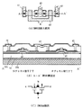
本実施例では、画素部及び駆動回路に使用するTFTを逆スタガ型TFTで構成した液晶表示装置の例を図16及び図17に示す。図16(A)は、画素部の画素の一つを拡大した上面図であり、図16(A)において、点線A−A'で切断した部分が、図16(B)の画素部の断面構造に相当する。
【0145】
図16(B)において、50aは基板ホルダー、51は金属基板、50bは下地絶縁膜であり、まず、実施の形態に従い、固定部で金属基板51を基板ホルダー50aに固定した後、下地絶縁膜50bを形成する。
【0146】
画素部において、画素TFT部はNチャネル型TFTで形成されている。基板上51にゲート電極52が形成され、その上に窒化珪素からなる第1絶縁膜53a、酸化珪素からなる第2絶縁膜53bが設けられている。また、第2絶縁膜上には、活性層としてn+ 領域54〜56と、チャネル形成領域57、58と、前記n+ 型領域とチャネル形成領域の間にn- 型領域59、60が形成される。また、チャネル形成領域57、58は絶縁層61、62で保護される。絶縁層61、62及び活性層を覆う第1の層間絶縁膜63にコンタクトホールを形成した後、n+ 領域54に接続する配線64が形成され、n+ 領域56にAlあるいはAg等からなる画素電極65が接続され、さらにその上にパッシベーション膜66が形成される。また、70は画素電極69と隣接する画素電極である。
【0147】
なお、本実施例では、画素部の画素TFTのゲート配線をダブルゲート構造としているが、オフ電流のバラツキを低減するために、トリプルゲート構造等のマルチゲート構造としても構わない。また、開口率を向上させるためにシングルゲート構造としてもよい。
【0148】
また、画素部の容量部は、第1絶縁膜及び第2絶縁膜を誘電体として、容量配線71と、n+ 領域56とで形成されている。
【0149】
なお、図16で示した画素部はあくまで一例に過ぎず、特に上記構成に限定されないことはいうまでもない。
【0150】
また、金属基板上の全てのTFTをNチャネル型TFTとすることができる。金属基板上の全てのTFTをNチャネル型TFTで構成すれば、Pチャネル型TFTを形成する工程を省略できるため、液晶表示装置の製造工程を簡略化することができる。また、それに伴って製造工程の歩留まりが向上し、液晶表示装置の製造コストを下げることができる。
【0151】
また、図17(A)は、駆動回路を構成するCMOS回路を拡大した上面図であり、図17(A)において、点線A−A'で切断した部分が、図17(B)の断面構造に相当する。また、このCMOS回路の回路図を図17(C)に示した。図17で示すCMOS回路はインバータ回路とも呼ばれ、半導体回路を構成する基本回路である。なお、図16と対応する箇所には同じ符号を用いた。
【0152】
図17(B)において、いずれのTFT(薄膜トランジスタ)も基板ホルダー50aに固定されたステンレス基板51上の下地絶縁膜50bに形成されている。CMOS回路のPチャネル型TFTには、ゲート電極40が形成され、その上に窒化珪素からなる第1絶縁膜、酸化珪素からなる第2絶縁膜が設けられている。第2絶縁膜上には、活性層としてp+ 領域(ドレイン領域、ソース領域)とチャネル形成領域とが形成される。本実施例では工程数を低減するため、Pチャネル型TFTに前記高濃度不純物領域と前記チャネル形成領域の間に低濃度不純物領域(LDD領域)を設けていないが、特に限定されず作製してもよい。チャネル形成領域は絶縁層で保護される。絶縁層及び半導体層を覆う第1の層間絶縁膜にコンタクトホールが形成され、p+ 領域に配線42、43が接続され、さらにその上にパッシベーションが形成される。
【0153】
また、Nチャネル型のTFTは、活性層としてn+ 領域(ソース領域)、n+ 領域(ドレイン領域)と、チャネル形成領域と、前記n+ 型領域とチャネル形成領域の間にn- 型領域が形成される。なお、ドレイン領域に接するn- 型領域はn- 型領域より幅を大きく形成して信頼性を向上させた。絶縁膜の上を覆う第1の層間絶縁膜にコンタクトホールが形成され、n+ 型領域には配線41、43が形成され、さらにその上にパッシベーション膜が形成される。なお、半導体層以外の部分は、上記Pチャネル型TFTと概略同一構造であり簡略化のため説明を省略する。
【0154】
このようなCMOS回路を組み合わせることで基本論理回路を構成したり、さらに複雑なロジック回路(信号分割回路、D/Aコンバータ、オペアンプ、γ補正回路など)をも構成することができ、さらにはメモリやマイクロプロセッサをも形成しうる。
【0155】
また、本実施例のCMOS回路を備えた駆動回路とNチャネル型TFTからなる画素TFTを備えた画素部とを同一基板上に形成したアクティブマトリクス基板を形成することができる。
【0156】
また、こうして得られるアクティブマトリクス基板を用いて、実施例1及び実施例5に従えば、同様に図9に示す液晶表示装置を形成することもできる。
【0157】
また、駆動回路及び画素の構造の他の一例として、図18に示すような断面構造としてもよい。このような構造とすることで開口率が向上する。なお、TFTの構造は図16とほぼ同一であるのでここでは説明を省略する。
【0158】
金属基板上の下地絶縁膜上にpチャネル型TFT11とnチャネル型TFT12を有する駆動回路15と、画素TFT13と保持容量14を有する画素部16が形成される。
【0159】
駆動回路15のpチャネル型TFT11には、チャネル形成領域、ソースまたはドレイン領域23が形成されている。接続電極26によってドレイン配線20とドレイン領域23が接続されている。nチャネル型TFT12には、チャネル形成領域、LDD領域、ソースまたはドレイン領域が形成されている。画素部16の画素TFT13は、マルチゲート構造であり、チャネル形成領域、LDD領域、ソースまたはドレイン領域24が形成される。保持容量14は、容量配線22と半導体層25とその間に形成される絶縁層とから形成されている。
【0160】
画素部16においては、接続電極30によりソース配線21は、画素TFT13のソースまたはドレイン領域24と電気的な接続が形成される。また、ゲート配線19は、電極31と電気的な接続が形成される。また、画素電極320は、画素TFT13のソースまたはドレイン領域及び保持容量14の半導体層25と接続している。
【0161】
また、本実施例は実施例1乃至3のいずれか一と自由に組み合わせることが可能である。
【0162】
[実施例9]
本願発明を実施して形成された駆動回路や画素部は様々な電気光学装置(アクティブマトリクス型液晶ディスプレイ、アクティブマトリクス型ECディスプレイ)に用いることができる。即ち、それら電気光学装置を表示部に組み込んだ電子機器全てに本願発明を実施できる。
【0163】
その様な電子機器としては、ビデオカメラ、デジタルカメラ、ヘッドマウントディスプレイ(ゴーグル型ディスプレイ)、カーナビゲーション、カーステレオ、パーソナルコンピュータ、携帯情報端末(モバイルコンピュータ、携帯電話または電子書籍等)などが挙げられる。それらの一例を図19及び図20に示す。
【0164】
図19(A)はパーソナルコンピュータであり、本体2001、画像入力部2002、表示部2003、キーボード2004等を含む。本発明を画像入力部2002、表示部2003やその他の駆動回路に適用することができる。
【0165】
図19(B)はビデオカメラであり、本体2101、表示部2102、音声入力部2103、操作スイッチ2104、バッテリー2105、受像部2106等を含む。本発明を表示部2102やその他の駆動回路に適用することができる。
【0166】
図19(C)はモバイルコンピュータ(モービルコンピュータ)であり、本体2201、カメラ部2202、受像部2203、操作スイッチ2204、表示部2205等を含む。本発明は表示部2205やその他の駆動回路に適用できる。
【0167】
図19(D)はゴーグル型ディスプレイであり、本体2301、表示部2302、アーム部2303等を含む。本発明は表示部2302やその他の駆動回路に適用することができる。
【0168】
図19(E)はプログラムを記録した記録媒体(以下、記録媒体と呼ぶ)を用いるプレーヤーであり、本体2401、表示部2402、スピーカ部2403、記録媒体2404、操作スイッチ2405等を含む。なお、このプレーヤーは記録媒体としてDVD(Digtial Versatile Disc)、CD等を用い、音楽鑑賞や映画鑑賞やゲームやインターネットを行うことができる。本発明は表示部2402やその他の駆動回路に適用することができる。
【0169】
図19(F)はデジタルカメラであり、本体2501、表示部2502、接眼部2503、操作スイッチ2504、受像部(図示しない)等を含む。本願発明を表示部2502やその他の駆動回路に適用することができる。
【0170】
図20(A)は携帯電話であり、本体2901、音声出力部2902、音声入力部2903、表示部2904、操作スイッチ2905、アンテナ2906等を含む。本願発明を音声出力部2902、音声入力部2903、表示部2904やその他の駆動回路に適用することができる。
【0171】
図20(B)は携帯書籍(電子書籍)であり、本体3001、表示部3002、3003、記憶媒体3004、操作スイッチ3005、アンテナ3006等を含む。本発明は表示部3002、3003やその他の駆動回路に適用することができる。
【0172】
図20(C)はディスプレイであり、本体3101、支持台3102、表示部3103等を含む。本発明は表示部3103に適用することができる。本発明のディスプレイは特に大画面化した場合において有利であり、対角10インチ以上(特に30インチ以上)のディスプレイには有利である。
【0173】
以上の様に、本願発明の適用範囲は極めて広く、あらゆる分野の電子機器に適用することが可能である。また、本実施例の電子機器は実施例1〜8のどのような組み合わせからなる構成を用いても実現することができる。
【0174】
【発明の効果】
本発明により、フレキシブルなフィルム上にTFT素子を形成して軽量化して安価な液晶表示装置を提供することができる。
【図面の簡単な説明】
【図1】 基板ホルダーに基板を固定する工程を示す図。
【図2】 作製工程を示す図。
【図3】 結晶質半導体膜の作製方法を説明する図。
【図4】 結晶質半導体膜の作製方法を説明する図。
【図5】 CMOS回路を作製する工程を説明する図。
【図6】 CMOS回路を作製する工程を説明する図。
【図7】 液晶表示装置の駆動回路及び画素部の断面構造図。
【図8】 液晶表示装置の画素の上面図。
【図9】 液晶表示装置の上面図。
【図10】 液晶表示装置の回路ブロック図。
【図11】 液晶表示装置の作製工程を示す図。
【図12】 液晶表示装置の作製工程を示す図。
【図13】 液晶表示装置の作製工程を示す図。
【図14】 液晶表示装置の作製工程を示す図。
【図15】 液晶表示装置の駆動回路(インバータ)の断面図。
【図16】 液晶表示装置の画素部の断面構造図。
【図17】 液晶表示装置の駆動回路(インバータ)の断面図。
【図18】 液晶表示装置の駆動回路及び画素部の断面構造図。
【図19】 電子機器の一例を示す図。
【図20】 電子機器の一例を示す図。
【図21】 TFTの特性を示す図。
【図22】 TFTの特性を示す図。[0001]
BACKGROUND OF THE INVENTION
The present invention relates to a semiconductor device having a circuit formed of a thin film transistor (hereinafter referred to as TFT) and a method for manufacturing the semiconductor device. For example, the present invention relates to an electro-optical device typified by a liquid crystal display panel and an electronic apparatus in which such an electro-optical device is mounted as a component.
[0002]
Note that in this specification, a semiconductor device refers to all devices that can function by utilizing semiconductor characteristics, and an electro-optical device, a semiconductor circuit, and an electronic device are all semiconductor devices.
[0003]
[Prior art]
In recent years, a technique for forming a thin film transistor (TFT) using a semiconductor thin film (having a thickness of about several to several hundred nm) formed on a substrate having an insulating surface has attracted attention. Thin film transistors are widely applied to electronic devices such as ICs and electro-optical devices, and development of switching devices for image display devices is urgently required.
[0004]
Various applications using such an image display device are expected, but the use for portable devices is attracting attention. Therefore, it has been attempted to form a TFT element on a flexible plastic film.
[0005]
However, since the heat resistance of the plastic film is low, the maximum temperature of the process has to be lowered, and as a result, TFTs having better electrical characteristics cannot be formed than when formed on a glass substrate. Therefore, a high-performance liquid crystal display device using a plastic film has not been realized.
[0006]
[Problems to be solved by the invention]
The present invention has been made in view of the above problems, and an object of the present invention is to provide a light-emitting element on a flexible film to reduce the weight and provide an inexpensive electro-optical device. Furthermore, it is an object to provide an inexpensive electric appliance having the display portion as a display unit.
[0007]
[Means for Solving the Problems]
The present invention is characterized in that a light-weight electro-optical device is obtained by forming a necessary element on a flexible metal substrate by using a thin metal substrate instead of a plastic substrate as an element formation substrate. Yes.
[0008]
Note that the necessary elements refer to semiconductor elements (typically TFTs) or MIM elements used as pixel switching elements in the case of an active matrix type electro-optical device.
[0009]
The configuration of the invention disclosed in this specification is as follows.
An insulating film over a substrate having a metal surface, a driver circuit and a pixel portion on the insulating film, a counter substrate, and a liquid crystal material between the counter substrate and the substrate having the metal surface. This is a semiconductor device.
[0010]
In the above structure, the substrate having the metal surface is a stainless steel substrate.
[0011]
In the above structure, the stainless steel substrate has a thickness of 10 μm to 30 μm.
[0012]
In the above structure, the surface roughness of the substrate having the metal surface is 1 μmR. MAX It is characterized by the following.
[0013]
In the above structure, the curvature radius of the convex portion existing on the surface of the substrate having the metal surface is 1 μm or more.
[0014]
In the above structure, the semiconductor device is a reflective liquid crystal display device.
[0015]
Further, in order to realize the above structure, the present invention is necessary on the thin metal substrate after bending the end portion of the thin metal substrate and fixing it in a vacuum with good adhesion to the substrate holder having the curvature at the end portion. In this case, a liquid crystal material is sealed and held after a fixed substrate is bonded to the device with an adhesive layer (sealing material or the like), and then the substrate holder is separated.
[0016]
The configuration of the invention for realizing the above structure is as follows.
Bending and fixing the end of the substrate having a metal surface to the substrate holder;
Forming an insulating film on the substrate having the metal surface;
Forming a TFT element and a pixel electrode on the insulating film;
Bonding a fixed substrate with an adhesive layer on the pixel electrode;
Separating the substrate substrate holder;
It is a semiconductor device characterized by having.
[0017]
In the above structure, the fixing step is performed in a vacuum.
[0018]
Moreover, the said structure WHEREIN: The said process to fix is performed at room temperature-400 degreeC, It is characterized by the above-mentioned.
[0019]
In the above configuration, the end of the substrate substrate holder has a curved surface.
[0020]
Further, in the above configuration, the substrate substrate holder has the same thermal expansion coefficient as that of the substrate having the metal surface.
[0021]
In the above structure, the substrate having the metal surface is a stainless steel substrate. The stainless substrate has a thickness of 10 μm to 30 μm.
[0022]
In the above configuration, the substrate substrate holder is a stainless steel substrate. The stainless substrate has a thickness of 500 μm to 1000 μm.
[0023]
In the above structure, a liquid crystal material is provided between the pixel electrode and the fixed substrate.
[0024]
The semiconductor device described in the above structure is a reflective liquid crystal display device.
[0025]
In addition, the stainless steel in this specification has pointed out the steel (iron-carbon alloy) which contains about 12% or more of chromium, and can be divided roughly into a martensite type, a ferrite type, and an austenite type | system | group on a composition. It also includes stainless steel to which one or more selected from Ti, Nb, Mo, Cu, Ni, or Si are added.
[0026]
DETAILED DESCRIPTION OF THE INVENTION
Embodiments of the present invention will be described below.
[0027]
First, a metal substrate 102 serving as an element formation substrate and a substrate holder 101 are prepared. As the metal substrate 102 (substrate having a metal surface), a stainless steel substrate is prepared. The substrate 102 has a thickness of 10 μm to 30 μm. As the substrate holder 101, a stainless steel substrate thicker than the metal substrate 102 is prepared. The substrate 101 has a thickness of 500 μm to 1000 μm. Further, as the substrate holder 101, ceramic or Al 2 O Three Can also be used.
[0028]
Next, as shown in FIG. 1A, the substrate holder 101 having at least a curved surface at the end and the metal substrate 102 are fixed so that air does not enter between them, and the end of the metal substrate 102 is further fixed using the fixing
[0029]
Moreover, the surface roughness of the surface irregularities on the metal substrate after fixing is 1 μmR MAX It is preferable to be flat as follows. Or it is preferable that the surface roughness per 1 mm square of the unevenness | corrugation of the surface in the metal substrate after fixation becomes 1 micrometer. Further, the radius of curvature of the uneven projection is 1 μm or more, preferably 10 μm or more. A known technique for improving the flatness of the surface of the metal substrate, for example, a polishing process called CMP (Chemical Mechanical Polishing) may be used.
[0030]
Next, after a base insulating film is formed over the metal substrate 102, necessary elements are formed over the base insulating film. Note that although the surface of the base insulating film is shown as a flat surface for simplification, a step is actually generated at a portion where the fixed portion and the metal substrate are in contact with each other. If the element formation substrate is a plastic substrate, the process temperature needs to be 350 ° C. or lower. However, since the element formation substrate is a metal substrate, heat treatment at 350 ° C. or higher is possible in the present invention. Note that it is preferable to match the thermal expansion coefficients of the substrate holder and the metal substrate so that the substrates are not separated from each other by the heat treatment in the element forming step. Here, an example in which the pixel portion 105 including the driver circuit 104 and the TFT element is formed is shown. (Figure 1 (C))
[0031]
Next, the fixed substrate 106 is bonded with an adhesive layer (sealing material) 107. Note that although the fixed substrate 106 is used here to hold the liquid crystal material 108, it may not be used unless particularly necessary. As the fixed substrate 106, a light-transmitting resin substrate or glass substrate may be used, and a substrate provided with a DLC film as a protective film on one side or both sides may be used.
[0032]
Next, after the liquid crystal material 108 is injected between the substrates, the injection port is sealed.
[0033]
Next, the substrate holder is removed by removing physical means, for example, the fixing
[0034]
Finally, a liquid crystal display device sandwiched between an element formation substrate which is a thin metal substrate 108 and a fixed substrate which is a resin substrate is completed. Note that this liquid crystal display device is a reflective type, and the pixel electrode connected to the TFT element in the pixel portion is formed of a highly reflective material.
[0035]
In FIG. 1 and FIG. 2, for simplicity, the end of the substrate holder and the TFT element are shown not far apart from each other, but it is actually preferable that the distance is sufficiently long.
[0036]
The present invention having the above-described configuration will be described in more detail with the following examples.
[0037]
【Example】
[Example 1]
In this embodiment, an example of a method for manufacturing a liquid crystal display device sandwiched between an element formation substrate which is a thin metal substrate and a fixed substrate which is a resin substrate will be described with reference to FIGS. However, it goes without saying that the present invention is not limited to this embodiment.
[0038]
First, a stainless steel substrate is used as the substrate holder 101. Then, the substrate holder 101 and the element formation substrate 102 which is a thin metal substrate were fixed by the fixing
[0039]
Next, after a base insulating film is formed over the metal substrate 102, necessary elements are formed over the base insulating film. Here, an example in which the pixel portion 105 including the driver circuit 104 and the TFT element is formed is shown. (Figure 1 (C))
[0040]
As the base insulating film, a silicon oxide film, a silicon nitride film, a silicon nitride oxide film (SiOx Ny), or a laminated film of these can be used in a film thickness range of 100 to 500 nm. A film method (thermal CVD method, plasma CVD method, vapor deposition method, sputtering method, reduced pressure thermal CVD method, or the like) is used. Here, a silicon oxynitride film containing more nitrogen element than oxygen element in the film composition and a silicon oxynitride film containing oxygen element more than nitrogen element in the film composition were stacked.
[0041]
Next, a semiconductor layer is formed over the base insulating film. The material of the semiconductor layer is not limited, but preferably silicon or silicon germanium (Si X Ge 1-X (0 <X <1)) It may be formed of an alloy or the like. As a forming means, a known film forming method (thermal CVD method, plasma CVD method, vapor deposition method, sputtering method, reduced pressure thermal CVD method, etc.) can be used, and a crystallization method is also known (solid phase growth method, laser). A crystallization method, a solid phase growth method using a catalytic element, etc.) can be used. In this embodiment, an amorphous silicon film is formed by a sputtering method that can be formed at a low temperature, and a crystalline silicon film is formed by a laser crystallization method. When a crystalline semiconductor film is formed by laser crystallization, a pulse oscillation type or continuous emission type excimer laser, YAG laser, YVO Four A laser can be used.
[0042]
Next, a gate insulating film covering the semiconductor layer is formed by a known method (thermal CVD method, plasma CVD method, vapor deposition method, sputtering method, reduced pressure thermal CVD method, or the like). In this embodiment, a silicon oxide film is formed using a plasma CVD method.
[0043]
Next, a conductive layer is formed over the gate insulating film. The conductive layer is formed by forming a conductive film by a known means (thermal CVD method, plasma CVD method, reduced pressure thermal CVD method, vapor deposition method, sputtering method, etc.) and then patterning it into a desired shape using a mask. To do.
[0044]
Next, an impurity region for forming an LDD region, a source region, or a drain region is formed by appropriately adding an impurity element imparting n-type conductivity or an impurity element imparting p-type conductivity to the semiconductor layer by an ion implantation method or an ion doping method. Form.
[0045]
Thereafter, an interlayer insulating film is formed using a silicon nitride film, a silicon nitride oxide film, or a silicon oxide film manufactured by a known method (thermal CVD method, plasma CVD method, vapor deposition method, sputtering method, reduced pressure thermal CVD method, or the like). . The added impurity element is activated. Here, laser light irradiation was performed. Instead of laser light irradiation, activation may be performed by heat treatment.
[0046]
Next, a contact hole reaching the source region or the drain region is formed using a known technique, and then a source electrode or a drain electrode is formed to obtain a TFT.
[0047]
Next, hydrogenation is performed using a known technique, and the whole is hydrogenated to complete an n-channel TFT or a p-channel TFT. In this embodiment, the hydrogenation treatment was performed using hydrogen plasma that can be performed at a relatively low temperature.
[0048]
Next, an interlayer insulating film is formed using a silicon nitride film, a silicon nitride oxide film, or a silicon oxide film manufactured by a known method (thermal CVD method, plasma CVD method, vapor deposition method, sputtering method, reduced pressure thermal CVD method, or the like). . Next, a contact hole reaching the drain electrode of the pixel portion is formed using a known technique, and then a pixel electrode (reflection electrode) is formed.
[0049]
Next, all elements included in the pixel portion and the driver circuit are covered with an insulating film (alignment film or the like).
[0050]
Next, the insulating film covering all the elements formed on the element formation substrate and the fixed substrate 106 are bonded together by the second adhesive layer (sealing material) 107. Thereafter, a liquid crystal material is injected and sealed. (FIG. 2 (A)) As the fixed substrate 106, a resin substrate may be used. A substrate provided with a DLC film as a protective film on one or both sides is provided, and a counter electrode and an alignment film for aligning liquid crystals are provided. ing.
[0051]
Next, the substrate holder is removed by removing physical means, for example, the fixing
[0052]
Finally, a liquid crystal display device in which a liquid crystal material is held by an element formation substrate which is a thin metal substrate and a fixed substrate which is a resin substrate is completed.
[0053]
[Example 2]
A method for selectively forming a crystalline semiconductor film using a metal element that promotes crystallization of an amorphous semiconductor film will be described with reference to FIGS. In FIG. 3A,
[0054]
First, the metal substrate and the substrate holder are fixed by a fixing portion by the method described in the embodiment, and the
[0055]
Next, an
[0056]
For crystallization, heat treatment is performed at a temperature of 500 to 650 ° C. for 4 to 24 hours, for example, at 570 ° C. for 14 hours. In this case, the portion of the amorphous silicon film in contact with nickel crystallizes first, and the crystallization proceeds in a direction parallel to the surface of the substrate. The
[0057]
Note that this embodiment can be combined with the first embodiment.
[0058]
[Example 3]
The metal element used in the crystallization remains in the crystalline silicon film manufactured according to the method described in the second embodiment. Even if it is not uniformly distributed in the film, the average concentration is 1 × 10 19 / Cm Three Remaining at a concentration exceeding Of course, even in such a state, it can be used for channel formation regions of various semiconductor devices including TFTs, but it is more preferable to remove the metal element by gettering.
[0059]
In this embodiment, an example of a gettering method will be described with reference to FIG. On the surface of the
[0060]
Then, as shown in FIG. 4B, when heat treatment is performed in a nitrogen atmosphere at 550 to 800 ° C. for 5 to 24 hours, for example, 600 ° C. for 12 hours, the phosphorus-added region 305 functions as a gettering site, The catalytic element remaining in the
[0061]
After that, as shown in FIG. 4C, the masking
[0062]
Note that this embodiment can be combined with
[0063]
[Example 4]
This embodiment is an example of manufacturing a CMOS circuit in which an n-channel TFT and a p-channel TFT are complementarily combined, and will be described with reference to FIGS.
[0064]
In accordance with the embodiment mode, the
[0065]
Next, a
[0066]
Next, as shown in FIG. 5C, a resist
[0067]
Under the above etching conditions, the end portion can be tapered by the shape of the resist mask and the effect of the bias voltage applied to the substrate side. The angle of the tapered portion is set to 15 to 45 °. In order to etch without leaving a residue on the gate insulating film, it is preferable to increase the etching time at a rate of about 10 to 20%. Since the selection ratio of the silicon oxynitride film to the W film is 2 to 4 (typically 3), the surface where the silicon oxynitride film is exposed is etched by about 20 to 50 nm by the over-etching process. Thus, first-shaped
[0068]
Then, a second etching process is performed as shown in FIG. The ICP etching method is used for etching, and CF is used as an etching gas. Four And Cl 2 And O 2 And 500 W of RF power (13.56 MHz) is supplied to the coil-type electrode at a pressure of 1 Pa to generate plasma. 50 W RF (13.56 MHz) power is applied to the substrate side (sample stage), and a lower self-bias voltage is applied than in the first etching process. Under such conditions, the tungsten film is anisotropically etched to leave the tantalum nitride film or titanium film as the first conductive layer. Thus, second shape
[0069]
Next, a first doping process is performed to dope n-type impurities (donors). (FIG. 6A) The method is performed by an ion doping method or an ion implantation method. As the impurity element imparting n-type, an element belonging to
[0070]
Next, after removing the mask, a
[0071]
Then, after removing the resist, as shown in FIG. 6C, a resist
[0072]
Through the above steps, impurity regions are formed in each island-like semiconductor layer. The second shape
[0073]
Further, a
[0074]
The
[0075]
Next, contact holes are formed, and source wirings or drain
[0076]
Through the above steps, a CMOS circuit in which an n-channel TFT and a p-channel TFT are combined in a complementary manner can be obtained.
[0077]
In addition, it cannot be overemphasized that the heat processing temperature in the above process shall be below the temperature which the
[0078]
The p-channel TFT has a
[0079]
The n-channel TFT includes a
[0080]
Such a CMOS circuit makes it possible to form a drive circuit for an active matrix liquid crystal display device. In addition, such an n-channel TFT or a p-channel TFT can be applied to a transistor forming the pixel portion.
[0081]
By combining such CMOS circuits, basic logic circuits can be configured, and more complex logic circuits (signal division circuits, D / A converters, operational amplifiers, γ correction circuits, etc.) can be configured, and memory It is also possible to form a microprocessor.
[0082]
In addition, this embodiment can be freely combined with any one of
[0083]
[Example 5]
Here, an example in which a liquid crystal display device is manufactured using the TFT obtained in Example 4 will be described below with reference to FIGS.
[0084]
FIG. 7 shows an example of a liquid crystal display device having a pixel portion and a driving circuit for driving the pixel portion on a stainless steel substrate fixed to a substrate holder (before the liquid crystal material is sealed). Note that a CMOS circuit serving as a basic unit is shown in the driver circuit, and one pixel is shown in the pixel portion. The TFT of the CMOS circuit and the pixel portion can be obtained according to the fourth embodiment.
[0085]
In FIG. 7,
[0086]
The description of the p-
[0087]
In this embodiment, the
[0088]
FIG. 7 is a cross-sectional view taken along a dotted line AA ′ in FIG. The conductive layer 712 functioning as a gate electrode also serves as one electrode of a storage capacitor of an adjacent pixel, and forms a capacitor in a portion overlapping with the
[0089]
After obtaining the state of FIG. 7, an alignment film is formed on the
[0090]
Next, a fixed substrate (counter substrate) is prepared. Next, after a colored layer and a light shielding layer are formed on the fixed substrate, a planarization film is formed. Next, a counter electrode made of a transparent conductive film was formed on the planarization film at least in the pixel portion, an alignment film was formed on the entire surface of the counter substrate, and a rubbing process was performed.
[0091]
Then, the stainless steel substrate on which the pixel portion and the driving circuit are formed and the fixed substrate are bonded together with an adhesive layer (a sealing material in this embodiment). A filler is mixed in the adhesive layer, and two substrates are bonded to each other with a uniform interval by the filler and the columnar spacer. Thereafter, a liquid crystal material is injected between both substrates and completely sealed with a sealant (not shown). A known liquid crystal material may be used as the liquid crystal material.
[0092]
Next, after the liquid crystal sealing (or sealing) process was performed, the substrate holder was separated as shown in the embodiment and Example 1. The state of the liquid crystal display device thereafter will be described with reference to FIG.
[0093]
The top view shown in FIG. 9 includes a pixel portion, a drive circuit, an external input terminal to which an FPC (Flexible Printed Circuit Board: Flexible Printed Circuit) is pasted, wiring 81 for connecting the external input terminal to the input portion of each circuit, and the like. The
[0094]
A
[0095]
Here, the
[0096]
In addition, a light-shielding layer is provided between adjacent pixels in the color filter to shield light other than the display area. Here, the light shielding layers 86a and 86b are also provided in the region covering the drive circuit. However, the region covering the drive circuit is covered with a cover when the liquid crystal display device is incorporated later as a display portion of an electronic device. It is good also as a structure which does not provide a light shielding layer. Moreover, when producing a required element on stainless steel, a light shielding layer may be formed on stainless steel.
[0097]
Further, without providing the light-shielding layer, between the second fixed substrate and the counter electrode, the colored layers constituting the color filter are appropriately disposed so as to be shielded from light by laminating a plurality of layers. The gap between the pixel electrodes) and the drive circuit may be shielded from light.
[0098]
An FPC 89 made of a base film and wiring is bonded to the external input terminal with an anisotropic conductive resin. Furthermore, the mechanical strength is increased by the reinforcing plate.
[0099]
A polarizing plate (not shown) is attached only to the fixed substrate.
[0100]
The liquid crystal display device manufactured as described above can be used as a display portion of various electronic devices.
[0101]
In addition, this embodiment can be freely combined with any one of
[0102]
[Example 6]
In this embodiment, an example of the circuit configuration of the liquid crystal display device shown in
[0103]
Note that FIG. 10A illustrates a circuit configuration for performing analog driving. In this embodiment, a source side driver circuit 90, a pixel portion 91, and a gate side driver circuit 92 are provided. Note that in this specification, the drive circuit is a generic name including a source side processing circuit and a gate side drive circuit.
[0104]
The source side driver circuit 90 includes a shift register 90a, a buffer 90b, and a sampling circuit (transfer gate) 90c. The gate side driving circuit 92 includes a shift register 92a, a
[0105]
In this embodiment, the pixel portion 91 includes a plurality of pixels, and each of the plurality of pixels is provided with a TFT element.
[0106]
Further, the source side driver circuit 90 and the gate side driver circuit 92 can be formed of all p-channel TFTs or all n-channel TFTs.
[0107]
Although not shown, a gate side drive circuit may be further provided on the opposite side of the gate side drive circuit 92 with the pixel portion 91 interposed therebetween.
[0108]
In the case of digital driving, a latch (A) 93b and a latch (B) 93c may be provided instead of the sampling circuit as shown in FIG. The source side driving circuit 93 includes a shift register 93a, a latch (A) 93b, a latch (B) 93c, a D / A converter 93d, and a buffer 93e. The gate
[0109]
Further, the source side driver circuit 93 and the gate
[0110]
Further, the source side driver circuit 93 and the gate
[0111]
In addition, the said structure is realizable according to the manufacturing process shown to the said Examples 1 thru | or 5. Further, although only the configuration of the pixel portion and the drive circuit is shown in this embodiment, a memory or a microprocessor can be formed according to the manufacturing process of this embodiment.
[0112]
[Example 7]
In this embodiment, an example of a method for manufacturing a liquid crystal display device, which is different from that in FIG. 7, will be described with reference to FIGS. However, since the manufacturing steps of Example 4 are substantially the same steps up to FIG. 5C and only the steps after FIG. 5C are different, detailed description of the same portions is omitted here.
[0113]
First, the
[0114]
Next, the
[0115]
Next, the crystalline semiconductor film is patterned using a mask using a photolithography method to form semiconductor layers 807 to 811. The state up to this point corresponds to FIG. Next, after forming a
[0116]
Next, after removing the mask insulating film, an insulating film 813 to be a gate insulating film is formed over the semiconductor layer, and a first
[0117]
Next, as shown in FIG. 12A, a resist
[0118]
Next, with the resist mask as it is, a first doping process is performed using the first shape conductive layer as a mask to dope n-type impurities (donors). (FIG. 12 (B)) For example, the acceleration voltage is set to 20 to 60 keV, and 1 × 10 13 ~ 5x10 14 / Cm 2 Impurity regions (n + regions) 821a to 821e are formed by performing the above-described dose amount. For example, the phosphorus (P) concentration in the impurity region (n + region) is 1 × 10 20 ~ 1x10 twenty one / Cm Three To be in the range.
[0119]
Next, a second etching process is performed as shown in FIG. 12C while the resist mask is left as it is. The ICP etching method is used for etching, and CF is used as an etching gas. Four And Cl 2 And O 2 And 500 W of RF power (13.56 MHz) is supplied to the coil-type electrode at a pressure of 1 Pa to generate plasma. 50 W RF (13.56 MHz) power is applied to the substrate side (sample stage), and a lower self-bias voltage is applied than in the first etching process. Under such conditions, the tungsten film is anisotropically etched to leave the tantalum nitride film or titanium film as the first conductive layer. Thus, second shape
[0120]
Next, a second doping process is performed while the resist mask is left as it is, and an n-type impurity (donor) is doped. (FIG. 12D) In this case, of the second shape conductive layers, the second conductive film serves as a mask for the element to be doped, and the acceleration voltage is appropriately adjusted (for example, 70 to 120 keV). Impurity regions (n− regions) 829a to 829e are formed by the impurity element that has passed through the tapered portion of the gate insulating film and the first conductive film. For example, the phosphorus (P) concentration in the impurity region (n− region) is 1 × 10. 17 ~ 1x10 19 / Cm Three To be in the range.
[0121]
Next, after removing the resist mask, a resist
[0122]
Next, after removing the resist
[0123]
Through the above steps, impurity regions are formed in the respective semiconductor layers. After that, as shown in FIG. 13C, a protective
[0124]
Further, hydrogenation treatment is performed. In this embodiment, the hydrogenation treatment was performed using hydrogen plasma that can be performed at a relatively low temperature.
[0125]
The
[0126]
Next, contact holes are formed, and source wirings or drain
[0127]
Through the above steps, a
[0128]
In the
[0129]
In the
[0130]
In the
[0131]
The n-channel TFT constituting the pixel TFT of the pixel portion 854 preferably has a TFT structure in which low off-current operation is important. An impurity region (LDD region) formed outside the channel formation region and the gate electrode. And an impurity region functioning as a source region or a drain region.
[0132]
In addition, an impurity element imparting p-type conductivity is added to each semiconductor layer functioning as one electrode of the storage capacitor 860 in the pixel portion 854. The storage capacitor 860 is formed using
[0133]
After the state shown in FIG. 14 is obtained in this manner, the liquid crystal display device shown in FIG. 9 can be formed by following Example 1 and Example 5.
[0134]
Further, if the
[0135]
The CMOS circuit shown in FIG. 15 is an inverter circuit.
[0136]
In FIG. 15,
[0137]
In the semiconductor layer of the P-channel TFT 877, a
[0138]
In the semiconductor layer of the n-channel TFT 878, a
[0139]
As described above, in this embodiment, the structure of the TFT for forming each circuit is optimized according to the circuit specifications required by the pixel circuit and the driver circuit by appropriately changing the
[0140]
Further, the characteristics of the TFT obtained by this example showed good values. Among them, the TFT characteristics (VI characteristics) of the pixel TFT are shown in FIG. Although gate leakage is also shown in the figure, it is sufficiently suppressed. In particular, the pixel TFT structure of the present invention is a structure that suppresses off-current and exhibits excellent mobility. The off current is a drain current that flows when the TFT is in an off state.
[0141]
FIG. 21 shows VI characteristic graphs of
[0142]
By adopting the structure of the present invention, the threshold value (Vth) indicating the voltage value at the rising point in the VI characteristic graph is 0.263 V, which is a very small and good value. It can be said that the smaller this difference is, the more the short channel effect is suppressed. In addition, mobility (μ FE ) Is 119.2 (cm 2 / Vs). The S value (subthreshold coefficient) indicating the reciprocal of the maximum slope at the rising portion of the IV curve was 0.196 (V / decade). Further, the off-current (I OFF2 ) Is 0.39 pA, and the on-current (I ON2 ) Indicates 70 μA. The off current is a drain current that flows when the TFT is in an on state. Shift-1 indicates the voltage value at the rise of the IV curve.
[0143]
In addition, this embodiment can be freely combined with any one of
[0144]
[Example 8]
In this embodiment, an example of a liquid crystal display device in which TFTs used for a pixel portion and a driving circuit are formed of inverted staggered TFTs is shown in FIGS. FIG. 16A is an enlarged top view of one of the pixels in the pixel portion. In FIG. 16A, a portion cut along a dotted line AA ′ is a cross section of the pixel portion in FIG. Corresponds to the structure.
[0145]
In FIG. 16B,
[0146]
In the pixel portion, the pixel TFT portion is formed of an N-channel TFT. A
[0147]
In this embodiment, the gate wiring of the pixel TFT in the pixel portion has a double gate structure. However, a multi-gate structure such as a triple gate structure may be used in order to reduce variation in off current. Further, a single gate structure may be used in order to improve the aperture ratio.
[0148]
The capacitor portion of the pixel portion is formed by the
[0149]
Note that the pixel portion illustrated in FIG. 16 is merely an example, and needless to say, the configuration is not particularly limited to the above configuration.
[0150]
Further, all TFTs on the metal substrate can be N-channel TFTs. If all TFTs on the metal substrate are composed of N-channel TFTs, the process of forming P-channel TFTs can be omitted, and the manufacturing process of the liquid crystal display device can be simplified. As a result, the yield of the manufacturing process is improved, and the manufacturing cost of the liquid crystal display device can be reduced.
[0151]
FIG. 17A is an enlarged top view of the CMOS circuit constituting the driver circuit. In FIG. 17A, a portion cut along a dotted line AA ′ is a cross-sectional structure of FIG. It corresponds to. A circuit diagram of this CMOS circuit is shown in FIG. The CMOS circuit shown in FIG. 17 is also called an inverter circuit, and is a basic circuit constituting a semiconductor circuit. In addition, the same code | symbol was used for the location corresponding to FIG.
[0152]
In FIG. 17B, all TFTs (thin film transistors) are formed on the
[0153]
The N channel type TFT has an n + region (source region), an n + region (drain region) as an active layer, a channel formation region, and an n − type region between the n + type region and the channel formation region. Is formed. It should be noted that the n− type region in contact with the drain region was formed wider than the n− type region to improve reliability. A contact hole is formed in the first interlayer insulating film covering the insulating film, wirings 41 and 43 are formed in the n + -type region, and a passivation film is further formed thereon. Note that portions other than the semiconductor layer have substantially the same structure as that of the P-channel TFT, and a description thereof is omitted for simplification.
[0154]
By combining such CMOS circuits, basic logic circuits can be configured, and more complex logic circuits (signal division circuits, D / A converters, operational amplifiers, γ correction circuits, etc.) can be configured, and memory Or a microprocessor can be formed.
[0155]
Further, it is possible to form an active matrix substrate in which a driving circuit having the CMOS circuit of this embodiment and a pixel portion having a pixel TFT made of an N-channel TFT are formed on the same substrate.
[0156]
Further, according to Example 1 and Example 5 using the active matrix substrate thus obtained, the liquid crystal display device shown in FIG. 9 can be similarly formed.
[0157]
Further, as another example of the structure of the driver circuit and the pixel, a cross-sectional structure as shown in FIG. 18 may be used. With such a structure, the aperture ratio is improved. Note that the structure of the TFT is almost the same as that in FIG.
[0158]
A
[0159]
In the p-
[0160]
In the pixel portion 16, the source wiring 21 is electrically connected to the source or drain
[0161]
In addition, this embodiment can be freely combined with any one of
[0162]
[Example 9]
The drive circuit and the pixel portion formed by implementing the present invention can be used in various electro-optical devices (active matrix liquid crystal display, active matrix EC display). That is, the present invention can be implemented in all electronic devices in which these electro-optical devices are incorporated in the display unit.
[0163]
Such electronic devices include video cameras, digital cameras, head mounted displays (goggles type displays), car navigation systems, car stereos, personal computers, personal digital assistants (mobile computers, mobile phones, electronic books, etc.) and the like. . Examples of these are shown in FIGS.
[0164]
FIG. 19A illustrates a personal computer, which includes a main body 2001, an image input portion 2002, a display portion 2003, a
[0165]
FIG. 19B illustrates a video camera, which includes a main body 2101, a display portion 2102, an
[0166]
FIG. 19C illustrates a mobile computer, which includes a main body 2201, a camera unit 2202, an
[0167]
FIG. 19D illustrates a goggle type display including a
[0168]
FIG. 19E shows a player using a recording medium (hereinafter referred to as a recording medium) on which a program is recorded, and includes a main body 2401, a
[0169]
FIG. 19F illustrates a digital camera, which includes a main body 2501, a
[0170]
FIG. 20A illustrates a mobile phone, which includes a
[0171]
FIG. 20B illustrates a portable book (electronic book), which includes a
[0172]
FIG. 20C illustrates a display, which includes a
[0173]
As described above, the application range of the present invention is extremely wide and can be applied to electronic devices in various fields. Moreover, the electronic apparatus of a present Example is realizable even if it uses the structure which consists of what combination of Examples 1-8.
[0174]
【The invention's effect】
According to the present invention, an inexpensive liquid crystal display device can be provided by forming a TFT element on a flexible film to reduce the weight.
[Brief description of the drawings]
FIG. 1 is a diagram showing a process of fixing a substrate to a substrate holder.
FIG. 2 shows a manufacturing process.
3A and 3B illustrate a method for manufacturing a crystalline semiconductor film.
4A to 4C illustrate a method for manufacturing a crystalline semiconductor film.
FIGS. 5A and 5B illustrate a process for manufacturing a CMOS circuit. FIGS.
6A and 6B illustrate a process for manufacturing a CMOS circuit.
FIG. 7 is a cross-sectional structure diagram of a driver circuit and a pixel portion of a liquid crystal display device.
FIG. 8 is a top view of a pixel of a liquid crystal display device.
FIG. 9 is a top view of a liquid crystal display device.
FIG. 10 is a circuit block diagram of a liquid crystal display device.
FIG. 11 illustrates a manufacturing process of a liquid crystal display device.
12A to 12C illustrate a manufacturing process of a liquid crystal display device.
FIGS. 13A and 13B illustrate a manufacturing process of a liquid crystal display device. FIGS.
FIG. 14 illustrates a manufacturing process of a liquid crystal display device.
FIG. 15 is a cross-sectional view of a driving circuit (inverter) of a liquid crystal display device.
FIG. 16 is a cross-sectional structure diagram of a pixel portion of a liquid crystal display device.
FIG. 17 is a cross-sectional view of a driving circuit (inverter) of a liquid crystal display device.
18 is a cross-sectional structure diagram of a driver circuit and a pixel portion of a liquid crystal display device.
FIG 19 illustrates an example of an electronic device.
FIG. 20 illustrates an example of an electronic device.
FIG. 21 is a graph showing characteristics of a TFT.
FIG. 22 is a graph showing characteristics of a TFT.
Claims (12)
前記金属表面を有する基板上に絶縁膜を形成し、
前記絶縁膜上にTFT及び画素電極を形成し、
前記画素電極上に接着層で固定基板を貼り合わせ、
前記金属表面を有する基板の端部と前記基板ホルダーの端部を除去することにより、前記金属表面を有する基板を前記基板ホルダーから分離することを特徴とする半導体装置の作製方法。By fixing the substrate having the metal surface to the substrate holder by bending the end portion of the substrate having the metal surface to the substrate holder,
Forming an insulating film on the substrate having the metal surface;
A TFT and a pixel electrode are formed on the insulating film,
Affixing a fixed substrate with an adhesive layer on the pixel electrode,
A method for manufacturing a semiconductor device, wherein the substrate having the metal surface is separated from the substrate holder by removing an end of the substrate having the metal surface and an end of the substrate holder.
Priority Applications (1)
| Application Number | Priority Date | Filing Date | Title |
|---|---|---|---|
| JP2000232528A JP4754677B2 (en) | 2000-07-31 | 2000-07-31 | Method for manufacturing semiconductor device |
Applications Claiming Priority (1)
| Application Number | Priority Date | Filing Date | Title |
|---|---|---|---|
| JP2000232528A JP4754677B2 (en) | 2000-07-31 | 2000-07-31 | Method for manufacturing semiconductor device |
Publications (3)
| Publication Number | Publication Date |
|---|---|
| JP2002049056A JP2002049056A (en) | 2002-02-15 |
| JP2002049056A5 JP2002049056A5 (en) | 2007-09-20 |
| JP4754677B2 true JP4754677B2 (en) | 2011-08-24 |
Family
ID=18725202
Family Applications (1)
| Application Number | Title | Priority Date | Filing Date |
|---|---|---|---|
| JP2000232528A Expired - Fee Related JP4754677B2 (en) | 2000-07-31 | 2000-07-31 | Method for manufacturing semiconductor device |
Country Status (1)
| Country | Link |
|---|---|
| JP (1) | JP4754677B2 (en) |
Families Citing this family (10)
| Publication number | Priority date | Publication date | Assignee | Title |
|---|---|---|---|---|
| JP4583568B2 (en) * | 2000-09-19 | 2010-11-17 | 株式会社半導体エネルギー研究所 | Method for manufacturing light emitting device |
| US6956324B2 (en) | 2000-08-04 | 2005-10-18 | Semiconductor Energy Laboratory Co., Ltd. | Semiconductor device and manufacturing method therefor |
| JP3643025B2 (en) * | 2000-10-20 | 2005-04-27 | シャープ株式会社 | Active matrix display device and manufacturing method thereof |
| JP4389447B2 (en) * | 2003-01-28 | 2009-12-24 | セイコーエプソン株式会社 | Manufacturing method of electro-optical device |
| TW594210B (en) * | 2003-08-28 | 2004-06-21 | Ind Tech Res Inst | A method for manufacturing a flexible panel for FPD |
| GB0323285D0 (en) * | 2003-10-04 | 2003-11-05 | Koninkl Philips Electronics Nv | Device and method of making a device having a patterned layer on a flexible substrate |
| JP4529414B2 (en) * | 2003-10-29 | 2010-08-25 | セイコーエプソン株式会社 | Method for manufacturing substrate for electro-optical device |
| KR100698692B1 (en) * | 2005-07-20 | 2007-03-23 | 삼성에스디아이 주식회사 | A Flat Panel Display |
| JP4653860B2 (en) * | 2009-03-31 | 2011-03-16 | パナソニック株式会社 | Flexible semiconductor device and manufacturing method thereof |
| CN106783682B (en) * | 2016-12-15 | 2019-11-22 | 武汉华星光电技术有限公司 | Flexible display screen producing device and production method |
Citations (1)
| Publication number | Priority date | Publication date | Assignee | Title |
|---|---|---|---|---|
| JPH10161095A (en) * | 1996-12-03 | 1998-06-19 | Citizen Watch Co Ltd | Liquid crystal display device |
Family Cites Families (1)
| Publication number | Priority date | Publication date | Assignee | Title |
|---|---|---|---|---|
| JP3249698B2 (en) * | 1994-12-15 | 2002-01-21 | シャープ株式会社 | Display device |
-
2000
- 2000-07-31 JP JP2000232528A patent/JP4754677B2/en not_active Expired - Fee Related
Patent Citations (1)
| Publication number | Priority date | Publication date | Assignee | Title |
|---|---|---|---|---|
| JPH10161095A (en) * | 1996-12-03 | 1998-06-19 | Citizen Watch Co Ltd | Liquid crystal display device |
Also Published As
| Publication number | Publication date |
|---|---|
| JP2002049056A (en) | 2002-02-15 |
Similar Documents
| Publication | Publication Date | Title |
|---|---|---|
| JP4845273B2 (en) | Semiconductor device and manufacturing method thereof | |
| JP6002814B2 (en) | Semiconductor device | |
| US6956324B2 (en) | Semiconductor device and manufacturing method therefor | |
| JP4666723B2 (en) | Method for manufacturing semiconductor device | |
| JP4727024B2 (en) | Method for manufacturing semiconductor device | |
| JP4118485B2 (en) | Method for manufacturing semiconductor device | |
| JP4566475B2 (en) | Method for manufacturing light emitting device | |
| JP4485078B2 (en) | Method for manufacturing semiconductor device | |
| JP5292217B2 (en) | Method for manufacturing semiconductor device and method for manufacturing electronic book | |
| JP4754677B2 (en) | Method for manufacturing semiconductor device | |
| JP4993826B2 (en) | Method for manufacturing semiconductor device | |
| JP3961310B2 (en) | Method for manufacturing semiconductor device | |
| JP4916620B2 (en) | Liquid crystal display device and electro-optical device | |
| JP3983460B2 (en) | Method for manufacturing semiconductor device | |
| JP5143272B2 (en) | Method for manufacturing EL display device | |
| JP2002064107A (en) | Method of manufacturing semiconductor | |
| JP4986347B2 (en) | Method for manufacturing semiconductor device |
Legal Events
| Date | Code | Title | Description |
|---|---|---|---|
| A521 | Written amendment |
Free format text: JAPANESE INTERMEDIATE CODE: A523 Effective date: 20070725 |
|
| A621 | Written request for application examination |
Free format text: JAPANESE INTERMEDIATE CODE: A621 Effective date: 20070725 |
|
| A977 | Report on retrieval |
Free format text: JAPANESE INTERMEDIATE CODE: A971007 Effective date: 20100831 |
|
| A131 | Notification of reasons for refusal |
Free format text: JAPANESE INTERMEDIATE CODE: A131 Effective date: 20100907 |
|
| A521 | Written amendment |
Free format text: JAPANESE INTERMEDIATE CODE: A523 Effective date: 20101102 |
|
| A131 | Notification of reasons for refusal |
Free format text: JAPANESE INTERMEDIATE CODE: A131 Effective date: 20110301 |
|
| A521 | Written amendment |
Free format text: JAPANESE INTERMEDIATE CODE: A523 Effective date: 20110421 |
|
| TRDD | Decision of grant or rejection written | ||
| A01 | Written decision to grant a patent or to grant a registration (utility model) |
Free format text: JAPANESE INTERMEDIATE CODE: A01 Effective date: 20110517 |
|
| A01 | Written decision to grant a patent or to grant a registration (utility model) |
Free format text: JAPANESE INTERMEDIATE CODE: A01 |
|
| A61 | First payment of annual fees (during grant procedure) |
Free format text: JAPANESE INTERMEDIATE CODE: A61 Effective date: 20110526 |
|
| FPAY | Renewal fee payment (event date is renewal date of database) |
Free format text: PAYMENT UNTIL: 20140603 Year of fee payment: 3 |
|
| R150 | Certificate of patent or registration of utility model |
Free format text: JAPANESE INTERMEDIATE CODE: R150 |
|
| FPAY | Renewal fee payment (event date is renewal date of database) |
Free format text: PAYMENT UNTIL: 20140603 Year of fee payment: 3 |
|
| R250 | Receipt of annual fees |
Free format text: JAPANESE INTERMEDIATE CODE: R250 |
|
| R250 | Receipt of annual fees |
Free format text: JAPANESE INTERMEDIATE CODE: R250 |
|
| R250 | Receipt of annual fees |
Free format text: JAPANESE INTERMEDIATE CODE: R250 |
|
| R250 | Receipt of annual fees |
Free format text: JAPANESE INTERMEDIATE CODE: R250 |
|
| LAPS | Cancellation because of no payment of annual fees |