JP4748967B2 - Method for manufacturing semiconductor device - Google Patents
Method for manufacturing semiconductor device Download PDFInfo
- Publication number
- JP4748967B2 JP4748967B2 JP2004311126A JP2004311126A JP4748967B2 JP 4748967 B2 JP4748967 B2 JP 4748967B2 JP 2004311126 A JP2004311126 A JP 2004311126A JP 2004311126 A JP2004311126 A JP 2004311126A JP 4748967 B2 JP4748967 B2 JP 4748967B2
- Authority
- JP
- Japan
- Prior art keywords
- conductive film
- layer
- insulating film
- mask
- film
- Prior art date
- Legal status (The legal status is an assumption and is not a legal conclusion. Google has not performed a legal analysis and makes no representation as to the accuracy of the status listed.)
- Expired - Fee Related
Links
- 239000004065 semiconductor Substances 0.000 title claims description 49
- 238000000034 method Methods 0.000 title claims description 40
- 238000004519 manufacturing process Methods 0.000 title claims description 12
- 238000005530 etching Methods 0.000 claims description 47
- 229910052721 tungsten Inorganic materials 0.000 claims description 30
- 239000010937 tungsten Substances 0.000 claims description 28
- 229910052782 aluminium Inorganic materials 0.000 claims description 27
- XAGFODPZIPBFFR-UHFFFAOYSA-N aluminium Chemical compound [Al] XAGFODPZIPBFFR-UHFFFAOYSA-N 0.000 claims description 26
- 230000008569 process Effects 0.000 claims description 21
- 239000010936 titanium Substances 0.000 claims description 17
- WFKWXMTUELFFGS-UHFFFAOYSA-N tungsten Chemical compound [W] WFKWXMTUELFFGS-UHFFFAOYSA-N 0.000 claims description 17
- 229910045601 alloy Inorganic materials 0.000 claims description 16
- 239000000956 alloy Substances 0.000 claims description 16
- 239000003870 refractory metal Substances 0.000 claims description 16
- 229910052719 titanium Inorganic materials 0.000 claims description 16
- -1 tungsten nitride Chemical class 0.000 claims description 15
- RTAQQCXQSZGOHL-UHFFFAOYSA-N Titanium Chemical compound [Ti] RTAQQCXQSZGOHL-UHFFFAOYSA-N 0.000 claims description 13
- 239000010949 copper Substances 0.000 claims description 13
- 229910052715 tantalum Inorganic materials 0.000 claims description 13
- NRTOMJZYCJJWKI-UHFFFAOYSA-N Titanium nitride Chemical compound [Ti]#N NRTOMJZYCJJWKI-UHFFFAOYSA-N 0.000 claims description 12
- 239000007769 metal material Substances 0.000 claims description 12
- GUVRBAGPIYLISA-UHFFFAOYSA-N tantalum atom Chemical compound [Ta] GUVRBAGPIYLISA-UHFFFAOYSA-N 0.000 claims description 11
- 150000001875 compounds Chemical class 0.000 claims description 10
- 229910052802 copper Inorganic materials 0.000 claims description 10
- NFFIWVVINABMKP-UHFFFAOYSA-N methylidynetantalum Chemical compound [Ta]#C NFFIWVVINABMKP-UHFFFAOYSA-N 0.000 claims description 10
- 229910003468 tantalcarbide Inorganic materials 0.000 claims description 10
- MTPVUVINMAGMJL-UHFFFAOYSA-N trimethyl(1,1,2,2,2-pentafluoroethyl)silane Chemical compound C[Si](C)(C)C(F)(F)C(F)(F)F MTPVUVINMAGMJL-UHFFFAOYSA-N 0.000 claims description 10
- 229910010272 inorganic material Inorganic materials 0.000 claims description 9
- 239000011147 inorganic material Substances 0.000 claims description 9
- 150000004767 nitrides Chemical class 0.000 claims description 9
- RYGMFSIKBFXOCR-UHFFFAOYSA-N Copper Chemical compound [Cu] RYGMFSIKBFXOCR-UHFFFAOYSA-N 0.000 claims description 8
- 239000011368 organic material Substances 0.000 claims description 8
- MZLGASXMSKOWSE-UHFFFAOYSA-N tantalum nitride Chemical compound [Ta]#N MZLGASXMSKOWSE-UHFFFAOYSA-N 0.000 claims description 8
- 238000010438 heat treatment Methods 0.000 claims description 7
- 238000012545 processing Methods 0.000 claims description 4
- 239000010410 layer Substances 0.000 description 293
- 239000010408 film Substances 0.000 description 252
- 239000011229 interlayer Substances 0.000 description 61
- 230000004888 barrier function Effects 0.000 description 54
- 239000000463 material Substances 0.000 description 38
- 238000002347 injection Methods 0.000 description 33
- 239000007924 injection Substances 0.000 description 33
- 239000000758 substrate Substances 0.000 description 29
- 239000004020 conductor Substances 0.000 description 21
- VYPSYNLAJGMNEJ-UHFFFAOYSA-N Silicium dioxide Chemical compound O=[Si]=O VYPSYNLAJGMNEJ-UHFFFAOYSA-N 0.000 description 19
- 229910052814 silicon oxide Inorganic materials 0.000 description 18
- 239000004973 liquid crystal related substance Substances 0.000 description 15
- XUIMIQQOPSSXEZ-UHFFFAOYSA-N Silicon Chemical compound [Si] XUIMIQQOPSSXEZ-UHFFFAOYSA-N 0.000 description 14
- 229910052710 silicon Inorganic materials 0.000 description 14
- 239000010703 silicon Substances 0.000 description 14
- 229910052751 metal Inorganic materials 0.000 description 13
- 239000002184 metal Substances 0.000 description 13
- 230000006870 function Effects 0.000 description 11
- 230000005525 hole transport Effects 0.000 description 11
- 239000004642 Polyimide Substances 0.000 description 8
- 230000015572 biosynthetic process Effects 0.000 description 8
- 229920001721 polyimide Polymers 0.000 description 8
- 239000000243 solution Substances 0.000 description 8
- 229910052783 alkali metal Inorganic materials 0.000 description 7
- 150000001340 alkali metals Chemical class 0.000 description 7
- 229910052784 alkaline earth metal Inorganic materials 0.000 description 7
- 150000001342 alkaline earth metals Chemical class 0.000 description 7
- 229920005989 resin Polymers 0.000 description 7
- 239000011347 resin Substances 0.000 description 7
- IJGRMHOSHXDMSA-UHFFFAOYSA-N Atomic nitrogen Chemical compound N#N IJGRMHOSHXDMSA-UHFFFAOYSA-N 0.000 description 6
- NIXOWILDQLNWCW-UHFFFAOYSA-N acrylic acid group Chemical group C(C=C)(=O)O NIXOWILDQLNWCW-UHFFFAOYSA-N 0.000 description 6
- 239000011521 glass Substances 0.000 description 6
- 239000000203 mixture Substances 0.000 description 6
- 230000001681 protective effect Effects 0.000 description 6
- 125000001424 substituent group Chemical group 0.000 description 6
- QVGXLLKOCUKJST-UHFFFAOYSA-N atomic oxygen Chemical compound [O] QVGXLLKOCUKJST-UHFFFAOYSA-N 0.000 description 5
- 239000001257 hydrogen Substances 0.000 description 5
- 229910052739 hydrogen Inorganic materials 0.000 description 5
- 239000001301 oxygen Substances 0.000 description 5
- 229910052760 oxygen Inorganic materials 0.000 description 5
- 229910052581 Si3N4 Inorganic materials 0.000 description 4
- 239000011248 coating agent Substances 0.000 description 4
- 238000000576 coating method Methods 0.000 description 4
- 239000013078 crystal Substances 0.000 description 4
- KPUWHANPEXNPJT-UHFFFAOYSA-N disiloxane Chemical class [SiH3]O[SiH3] KPUWHANPEXNPJT-UHFFFAOYSA-N 0.000 description 4
- HQVNEWCFYHHQES-UHFFFAOYSA-N silicon nitride Chemical compound N12[Si]34N5[Si]62N3[Si]51N64 HQVNEWCFYHHQES-UHFFFAOYSA-N 0.000 description 4
- 238000004544 sputter deposition Methods 0.000 description 4
- 239000000126 substance Substances 0.000 description 4
- 239000010409 thin film Substances 0.000 description 4
- PXGOKWXKJXAPGV-UHFFFAOYSA-N Fluorine Chemical compound FF PXGOKWXKJXAPGV-UHFFFAOYSA-N 0.000 description 3
- UFHFLCQGNIYNRP-UHFFFAOYSA-N Hydrogen Chemical compound [H][H] UFHFLCQGNIYNRP-UHFFFAOYSA-N 0.000 description 3
- PXHVJJICTQNCMI-UHFFFAOYSA-N Nickel Chemical compound [Ni] PXHVJJICTQNCMI-UHFFFAOYSA-N 0.000 description 3
- KDLHZDBZIXYQEI-UHFFFAOYSA-N Palladium Chemical compound [Pd] KDLHZDBZIXYQEI-UHFFFAOYSA-N 0.000 description 3
- 239000004952 Polyamide Substances 0.000 description 3
- 125000000217 alkyl group Chemical group 0.000 description 3
- 150000001408 amides Chemical class 0.000 description 3
- 238000004458 analytical method Methods 0.000 description 3
- 150000004945 aromatic hydrocarbons Chemical class 0.000 description 3
- 239000002585 base Substances 0.000 description 3
- UMIVXZPTRXBADB-UHFFFAOYSA-N benzocyclobutene Chemical compound C1=CC=C2CCC2=C1 UMIVXZPTRXBADB-UHFFFAOYSA-N 0.000 description 3
- 238000009792 diffusion process Methods 0.000 description 3
- 230000000694 effects Effects 0.000 description 3
- 239000011737 fluorine Substances 0.000 description 3
- 229910052731 fluorine Inorganic materials 0.000 description 3
- 239000010931 gold Substances 0.000 description 3
- 239000012535 impurity Substances 0.000 description 3
- 238000010030 laminating Methods 0.000 description 3
- 150000002739 metals Chemical class 0.000 description 3
- 229910000476 molybdenum oxide Inorganic materials 0.000 description 3
- 229910052757 nitrogen Inorganic materials 0.000 description 3
- 150000002894 organic compounds Chemical class 0.000 description 3
- PQQKPALAQIIWST-UHFFFAOYSA-N oxomolybdenum Chemical compound [Mo]=O PQQKPALAQIIWST-UHFFFAOYSA-N 0.000 description 3
- BASFCYQUMIYNBI-UHFFFAOYSA-N platinum Chemical compound [Pt] BASFCYQUMIYNBI-UHFFFAOYSA-N 0.000 description 3
- 229920002647 polyamide Polymers 0.000 description 3
- 238000004528 spin coating Methods 0.000 description 3
- 229910018459 Al—Ge Inorganic materials 0.000 description 2
- 229910004261 CaF 2 Inorganic materials 0.000 description 2
- 102100040844 Dual specificity protein kinase CLK2 Human genes 0.000 description 2
- 101000749291 Homo sapiens Dual specificity protein kinase CLK2 Proteins 0.000 description 2
- JUJWROOIHBZHMG-UHFFFAOYSA-N Pyridine Chemical class C1=CC=NC=C1 JUJWROOIHBZHMG-UHFFFAOYSA-N 0.000 description 2
- XHCLAFWTIXFWPH-UHFFFAOYSA-N [O-2].[O-2].[O-2].[O-2].[O-2].[V+5].[V+5] Chemical compound [O-2].[O-2].[O-2].[O-2].[O-2].[V+5].[V+5] XHCLAFWTIXFWPH-UHFFFAOYSA-N 0.000 description 2
- IVHJCRXBQPGLOV-UHFFFAOYSA-N azanylidynetungsten Chemical compound [W]#N IVHJCRXBQPGLOV-UHFFFAOYSA-N 0.000 description 2
- 230000008901 benefit Effects 0.000 description 2
- 238000006243 chemical reaction Methods 0.000 description 2
- 239000011651 chromium Substances 0.000 description 2
- 150000004696 coordination complex Chemical class 0.000 description 2
- 238000001312 dry etching Methods 0.000 description 2
- 229910052732 germanium Inorganic materials 0.000 description 2
- 229910052737 gold Inorganic materials 0.000 description 2
- 150000002431 hydrogen Chemical class 0.000 description 2
- 229910003437 indium oxide Inorganic materials 0.000 description 2
- PJXISJQVUVHSOJ-UHFFFAOYSA-N indium(iii) oxide Chemical compound [O-2].[O-2].[O-2].[In+3].[In+3] PJXISJQVUVHSOJ-UHFFFAOYSA-N 0.000 description 2
- 239000003550 marker Substances 0.000 description 2
- 229910044991 metal oxide Inorganic materials 0.000 description 2
- 150000004706 metal oxides Chemical class 0.000 description 2
- 230000005012 migration Effects 0.000 description 2
- 238000013508 migration Methods 0.000 description 2
- IBHBKWKFFTZAHE-UHFFFAOYSA-N n-[4-[4-(n-naphthalen-1-ylanilino)phenyl]phenyl]-n-phenylnaphthalen-1-amine Chemical compound C1=CC=CC=C1N(C=1C2=CC=CC=C2C=CC=1)C1=CC=C(C=2C=CC(=CC=2)N(C=2C=CC=CC=2)C=2C3=CC=CC=C3C=CC=2)C=C1 IBHBKWKFFTZAHE-UHFFFAOYSA-N 0.000 description 2
- 230000002093 peripheral effect Effects 0.000 description 2
- 238000000206 photolithography Methods 0.000 description 2
- 229920002120 photoresistant polymer Polymers 0.000 description 2
- 238000005268 plasma chemical vapour deposition Methods 0.000 description 2
- 238000005498 polishing Methods 0.000 description 2
- 229920000139 polyethylene terephthalate Polymers 0.000 description 2
- 239000005020 polyethylene terephthalate Substances 0.000 description 2
- 230000007261 regionalization Effects 0.000 description 2
- 239000002344 surface layer Substances 0.000 description 2
- 230000008961 swelling Effects 0.000 description 2
- 229910001935 vanadium oxide Inorganic materials 0.000 description 2
- 238000001039 wet etching Methods 0.000 description 2
- BCMCBBGGLRIHSE-UHFFFAOYSA-N 1,3-benzoxazole Chemical class C1=CC=C2OC=NC2=C1 BCMCBBGGLRIHSE-UHFFFAOYSA-N 0.000 description 1
- 229910000838 Al alloy Inorganic materials 0.000 description 1
- 229910021364 Al-Si alloy Inorganic materials 0.000 description 1
- 229910018182 Al—Cu Inorganic materials 0.000 description 1
- 229910018575 Al—Ti Inorganic materials 0.000 description 1
- JBRZTFJDHDCESZ-UHFFFAOYSA-N AsGa Chemical compound [As]#[Ga] JBRZTFJDHDCESZ-UHFFFAOYSA-N 0.000 description 1
- OKTJSMMVPCPJKN-UHFFFAOYSA-N Carbon Chemical compound [C] OKTJSMMVPCPJKN-UHFFFAOYSA-N 0.000 description 1
- VYZAMTAEIAYCRO-UHFFFAOYSA-N Chromium Chemical compound [Cr] VYZAMTAEIAYCRO-UHFFFAOYSA-N 0.000 description 1
- 102100040862 Dual specificity protein kinase CLK1 Human genes 0.000 description 1
- 229910001218 Gallium arsenide Inorganic materials 0.000 description 1
- 101000749294 Homo sapiens Dual specificity protein kinase CLK1 Proteins 0.000 description 1
- XEEYBQQBJWHFJM-UHFFFAOYSA-N Iron Chemical compound [Fe] XEEYBQQBJWHFJM-UHFFFAOYSA-N 0.000 description 1
- 229910015711 MoOx Inorganic materials 0.000 description 1
- ZOKXTWBITQBERF-UHFFFAOYSA-N Molybdenum Chemical compound [Mo] ZOKXTWBITQBERF-UHFFFAOYSA-N 0.000 description 1
- 229920001609 Poly(3,4-ethylenedioxythiophene) Polymers 0.000 description 1
- 229920012266 Poly(ether sulfone) PES Polymers 0.000 description 1
- 229910004298 SiO 2 Inorganic materials 0.000 description 1
- 229910000577 Silicon-germanium Inorganic materials 0.000 description 1
- 229910002808 Si–O–Si Inorganic materials 0.000 description 1
- XLOMVQKBTHCTTD-UHFFFAOYSA-N Zinc monoxide Chemical compound [Zn]=O XLOMVQKBTHCTTD-UHFFFAOYSA-N 0.000 description 1
- LEVVHYCKPQWKOP-UHFFFAOYSA-N [Si].[Ge] Chemical compound [Si].[Ge] LEVVHYCKPQWKOP-UHFFFAOYSA-N 0.000 description 1
- 230000002411 adverse Effects 0.000 description 1
- 239000005407 aluminoborosilicate glass Substances 0.000 description 1
- 229910052787 antimony Inorganic materials 0.000 description 1
- 229910052788 barium Inorganic materials 0.000 description 1
- DSAJWYNOEDNPEQ-UHFFFAOYSA-N barium atom Chemical compound [Ba] DSAJWYNOEDNPEQ-UHFFFAOYSA-N 0.000 description 1
- 230000000903 blocking effect Effects 0.000 description 1
- 239000005388 borosilicate glass Substances 0.000 description 1
- 229910052792 caesium Inorganic materials 0.000 description 1
- 229910052791 calcium Inorganic materials 0.000 description 1
- 239000003990 capacitor Substances 0.000 description 1
- 229910052799 carbon Inorganic materials 0.000 description 1
- 150000001722 carbon compounds Chemical class 0.000 description 1
- 230000008859 change Effects 0.000 description 1
- 229910052804 chromium Inorganic materials 0.000 description 1
- 229910017052 cobalt Inorganic materials 0.000 description 1
- 239000010941 cobalt Substances 0.000 description 1
- GUTLYIVDDKVIGB-UHFFFAOYSA-N cobalt atom Chemical compound [Co] GUTLYIVDDKVIGB-UHFFFAOYSA-N 0.000 description 1
- 239000003086 colorant Substances 0.000 description 1
- 239000002131 composite material Substances 0.000 description 1
- 238000007796 conventional method Methods 0.000 description 1
- XCJYREBRNVKWGJ-UHFFFAOYSA-N copper(II) phthalocyanine Chemical compound [Cu+2].C12=CC=CC=C2C(N=C2[N-]C(C3=CC=CC=C32)=N2)=NC1=NC([C]1C=CC=CC1=1)=NC=1N=C1[C]3C=CC=CC3=C2[N-]1 XCJYREBRNVKWGJ-UHFFFAOYSA-N 0.000 description 1
- 230000007547 defect Effects 0.000 description 1
- 230000018044 dehydration Effects 0.000 description 1
- 238000006297 dehydration reaction Methods 0.000 description 1
- 238000010586 diagram Methods 0.000 description 1
- 239000002019 doping agent Substances 0.000 description 1
- 238000005401 electroluminescence Methods 0.000 description 1
- 238000010304 firing Methods 0.000 description 1
- 229910052733 gallium Inorganic materials 0.000 description 1
- 239000007789 gas Substances 0.000 description 1
- PCHJSUWPFVWCPO-UHFFFAOYSA-N gold Chemical compound [Au] PCHJSUWPFVWCPO-UHFFFAOYSA-N 0.000 description 1
- 238000000227 grinding Methods 0.000 description 1
- 238000007654 immersion Methods 0.000 description 1
- 230000001771 impaired effect Effects 0.000 description 1
- 230000006872 improvement Effects 0.000 description 1
- 229910052738 indium Inorganic materials 0.000 description 1
- AMGQUBHHOARCQH-UHFFFAOYSA-N indium;oxotin Chemical compound [In].[Sn]=O AMGQUBHHOARCQH-UHFFFAOYSA-N 0.000 description 1
- 239000012212 insulator Substances 0.000 description 1
- 229910052745 lead Inorganic materials 0.000 description 1
- 239000007788 liquid Substances 0.000 description 1
- 229910052744 lithium Inorganic materials 0.000 description 1
- 230000005923 long-lasting effect Effects 0.000 description 1
- 238000004518 low pressure chemical vapour deposition Methods 0.000 description 1
- 229910052749 magnesium Inorganic materials 0.000 description 1
- 125000002496 methyl group Chemical group [H]C([H])([H])* 0.000 description 1
- 230000004048 modification Effects 0.000 description 1
- 238000012986 modification Methods 0.000 description 1
- 229910052750 molybdenum Inorganic materials 0.000 description 1
- 239000011733 molybdenum Substances 0.000 description 1
- 229910052759 nickel Inorganic materials 0.000 description 1
- 229910017464 nitrogen compound Inorganic materials 0.000 description 1
- 150000002830 nitrogen compounds Chemical class 0.000 description 1
- 125000000962 organic group Chemical group 0.000 description 1
- 239000003960 organic solvent Substances 0.000 description 1
- JMANVNJQNLATNU-UHFFFAOYSA-N oxalonitrile Chemical compound N#CC#N JMANVNJQNLATNU-UHFFFAOYSA-N 0.000 description 1
- 238000004806 packaging method and process Methods 0.000 description 1
- 229910052763 palladium Inorganic materials 0.000 description 1
- 230000000149 penetrating effect Effects 0.000 description 1
- 230000000737 periodic effect Effects 0.000 description 1
- 125000001997 phenyl group Chemical group [H]C1=C([H])C([H])=C(*)C([H])=C1[H] 0.000 description 1
- 239000000049 pigment Substances 0.000 description 1
- 239000004033 plastic Substances 0.000 description 1
- 229920003023 plastic Polymers 0.000 description 1
- 229910052697 platinum Inorganic materials 0.000 description 1
- 239000011112 polyethylene naphthalate Substances 0.000 description 1
- 229920000642 polymer Polymers 0.000 description 1
- 229920001296 polysiloxane Polymers 0.000 description 1
- 239000011241 protective layer Substances 0.000 description 1
- UMJSCPRVCHMLSP-UHFFFAOYSA-N pyridine Chemical class COC1=CC=CN=C1 UMJSCPRVCHMLSP-UHFFFAOYSA-N 0.000 description 1
- 239000010453 quartz Substances 0.000 description 1
- 239000013079 quasicrystal Substances 0.000 description 1
- 229910052761 rare earth metal Inorganic materials 0.000 description 1
- 150000002910 rare earth metals Chemical class 0.000 description 1
- 230000003252 repetitive effect Effects 0.000 description 1
- YYMBJDOZVAITBP-UHFFFAOYSA-N rubrene Chemical compound C1=CC=CC=C1C(C1=C(C=2C=CC=CC=2)C2=CC=CC=C2C(C=2C=CC=CC=2)=C11)=C(C=CC=C2)C2=C1C1=CC=CC=C1 YYMBJDOZVAITBP-UHFFFAOYSA-N 0.000 description 1
- 229910052709 silver Inorganic materials 0.000 description 1
- 239000010944 silver (metal) Substances 0.000 description 1
- 239000002356 single layer Substances 0.000 description 1
- 125000006850 spacer group Chemical group 0.000 description 1
- 230000007480 spreading Effects 0.000 description 1
- 238000003892 spreading Methods 0.000 description 1
- 229910052712 strontium Inorganic materials 0.000 description 1
- 229920003002 synthetic resin Polymers 0.000 description 1
- 239000000057 synthetic resin Substances 0.000 description 1
- 229910052718 tin Inorganic materials 0.000 description 1
- 229910052723 transition metal Inorganic materials 0.000 description 1
- 150000003624 transition metals Chemical class 0.000 description 1
- 238000007740 vapor deposition Methods 0.000 description 1
- 238000000927 vapour-phase epitaxy Methods 0.000 description 1
- XLYOFNOQVPJJNP-UHFFFAOYSA-N water Chemical compound O XLYOFNOQVPJJNP-UHFFFAOYSA-N 0.000 description 1
- 229910052725 zinc Inorganic materials 0.000 description 1
- 239000011701 zinc Substances 0.000 description 1
- YVTHLONGBIQYBO-UHFFFAOYSA-N zinc indium(3+) oxygen(2-) Chemical compound [O--].[Zn++].[In+3] YVTHLONGBIQYBO-UHFFFAOYSA-N 0.000 description 1
Images


Description
本発明は、多層配線構造を備えた半導体装置に関し、特に層間絶縁膜を介して配線間の接続を形成する技術に関する。 The present invention relates to a semiconductor device having a multilayer wiring structure, and more particularly to a technique for forming a connection between wirings through an interlayer insulating film.
複数の回路素子が基板上又は基板内に集積された所謂半導体集積回路の配線構造として、層間絶縁膜と呼ばれる酸化珪素などの絶縁膜で異なる配線層間を電気的に絶縁分離した多層配線構造が知られている。 As a wiring structure of a so-called semiconductor integrated circuit in which a plurality of circuit elements are integrated on or in a substrate, a multilayer wiring structure in which different wiring layers are electrically insulated and separated by an insulating film such as silicon oxide called an interlayer insulating film is known. It has been.
層間絶縁膜を介して形成された配線間の導通をとる場合、コンタクトホールと呼ばれる開孔を層間絶縁膜に形成して導通をとる方法が用いられている。また、半導体集積回路の微細化技術では、上層配線と下層配線の間に柱状の導電性部材を介在させてコンタクトを形成する方法も開発されている。例えば、下層配線上に凸状の導電性部材を設け、上層配線とのコンタクトを形成する技術が開示されている(特許文献1及び2参照。)。
多層配線構造を形成する場合には、配線の形成工程や異なる配線間で電気的な接続を形成する工程が複雑でなく、なるべく簡素であることが望まれている。 In the case of forming a multilayer wiring structure, it is desired that the wiring forming process and the process of forming an electrical connection between different wirings are not complicated and as simple as possible.
しかしながら、従来の技術のように、下層配線若しくは下層配線用の導電膜を形成した後、その上に凸状の導電性部材を形成する方法では、下層配線用の導電膜と凸状の導電性部材を形成する導電膜との間にエッチングストッパーとなる導電性の被膜を介在させない限り加工することができないので、材料の選択肢が狭くなってしまうことが問題となる。 However, in the conventional method, after forming a conductive film for a lower layer wiring or a lower layer wiring and forming a convex conductive member thereon, the conductive film for the lower layer wiring and the convex conductive layer are formed. Since it cannot be processed unless a conductive film serving as an etching stopper is interposed between the conductive film forming the member, there is a problem that the choice of materials becomes narrow.
また、下層配線を形成する導電膜と凸状の導電性部材を形成するための導電膜を一度に形成する工程を採用すると合計の膜厚が厚くなり、フォトリソグラフィーの工程において下層に形成したアライメントマーカーと呼ばれる凸状の識別パターンが埋め込まれてしまう。そのために、CCDなどのカメラを用いたアライメントが困難になり、フォトマスクを精度良く位置合わせ出来なくなる。従って、微細なパターンの形成が著しく阻害されるといったことが問題となる。 In addition, if the process of forming the conductive film for forming the lower layer wiring and the conductive film for forming the convex conductive member at the same time is adopted, the total film thickness increases, and the alignment formed in the lower layer in the photolithography process. A convex identification pattern called a marker is embedded. For this reason, alignment using a camera such as a CCD becomes difficult, and the photomask cannot be accurately aligned. Therefore, there is a problem that the formation of a fine pattern is significantly inhibited.
本発明は、このような問題点を解決するためのものであり、微細でかつ信頼性の高い多層配線構造を、容易に形成することができる技術を提供することを目的としている。 The present invention has been made to solve such problems, and it is an object of the present invention to provide a technique capable of easily forming a fine and highly reliable multilayer wiring structure.
本発明は、アスペクト比(コンタクトホールの径と深さの比)の高いコンタクトホールを形成することを必要とせずに、多層配線間の接続を容易に実現することができる技術を提供する。これは、層間絶縁膜に隔てられた上層配線と下層配線の導通をとる箇所において、下層配線に凸状部(「プラグ」若しくは「ピラー」ともいう。)を設け、それを介して上層配線との電気的な接続を形成する。 The present invention provides a technique capable of easily realizing connection between multilayer wirings without requiring formation of a contact hole having a high aspect ratio (ratio of contact hole diameter to depth). This is because a convex portion (also referred to as a “plug” or “pillar”) is provided in the lower layer wiring at a location where the upper layer wiring and the lower layer wiring are separated by the interlayer insulating film, and the upper layer wiring is connected thereto. Form an electrical connection.
本発明は、下層配線の上方に絶縁層を介して配設される上層配線との電気的な接続を、下層配線に設けられた凸状部において形成した多層配線構造としたものである。凸状部は、柱状の導電性部材とその上層及び下層に形成されたものであり、下層配線の全体に渡って形成された導電膜とで構成され、上層配線は、凸状部が絶縁層の上面と略同一平面で露出した部箇所で、下層配線と電気的に接続していることを特徴としている。 The present invention has a multilayer wiring structure in which an electrical connection with an upper layer wiring disposed via an insulating layer above a lower layer wiring is formed in a convex portion provided in the lower layer wiring. The convex part is formed of a columnar conductive member and an upper layer and a lower layer thereof, and is composed of a conductive film formed over the entire lower layer wiring. It is characterized in that it is electrically connected to the lower layer wiring at a portion exposed in substantially the same plane as the upper surface of the wiring.
本発明は、コンタクトホールが形成された第1の絶縁膜と、第1の絶縁膜上に形成された第1の配線と前記第1の配線の上方に、第2の絶縁膜を介して配設された第2の配線とを有した多層配線構造を有し、第1の配線と第2の配線との電気的な接続を、第1配線に設けられた凸状部において形成し、コンタクトホールは、柱状の導電性部材と同一若しくは同様な材質の導電性材料で充填されている。さらに、凸状部は、凸状部を形成する柱状の導電性部材と、その上層及び下層に形成され、前記下層配線の全体に渡って形成された導電膜とで形成されることで、第2の配線は、凸状部が前記第2の絶縁膜の上面と略同一平面で露出した部箇所で、第1の配線と電気的に接続することを可能としていることを特徴としている。 The present invention provides a first insulating film in which a contact hole is formed, a first wiring formed on the first insulating film, and a first insulating film above the first wiring via a second insulating film. A multi-layer wiring structure having a second wiring provided, and an electrical connection between the first wiring and the second wiring is formed in a convex portion provided in the first wiring, and a contact The holes are filled with a conductive material that is the same as or similar to the columnar conductive member. Further, the convex portion is formed by a columnar conductive member that forms the convex portion, and a conductive film that is formed in the upper layer and the lower layer and formed over the entire lower layer wiring. The second wiring is characterized in that the convex portion can be electrically connected to the first wiring at a portion where the convex portion is exposed in substantially the same plane as the upper surface of the second insulating film.
柱状の導電性部材は、アルミニウム若しくはアルミニウムを主成分とする金属材料で形成され、柱状の導電性部材の上層及び下層に形成される導電膜は、チタン、タンタル、タングステンから選ばれた高融点金属、若しくは該高融点金属の窒化物から選ばれた一種で形成することが好ましい。 The columnar conductive member is made of aluminum or a metal material mainly composed of aluminum, and the conductive film formed in the upper and lower layers of the columnar conductive member is a refractory metal selected from titanium, tantalum, and tungsten. Alternatively, it is preferably formed of one kind selected from nitrides of the refractory metal.
凸状部、すなわち下層配線と上層配線を接続するプラグは、単層又は複数の層を積層して形成する。複数の層を積層する場合には、凸状部を形成する導電性部材の上下層及び側面を、耐熱性又は耐エレクトロマイグレーション性のある導電性材料で被覆するように形成する。すなわち、Al、Cu、Ag、Auその他の金属材料で形成された導電性部材を、該金属の拡散を防止することのできるバリア性を有する導電膜で被覆することが好ましい。このバリア性を有する導電膜(以下、「バリア層」ともいう。)としては、Ti、Ta、Wや、Ti、Ta、Wの窒素化合物若しくは炭素化合物などから選ばれた一種類または数種類の材料を用いることができる。バリア層は上記材料からなる一層若しくは複数層を積層して形成することができる。 The convex portion, that is, the plug connecting the lower layer wiring and the upper layer wiring is formed by laminating a single layer or a plurality of layers. When a plurality of layers are stacked, the upper and lower layers and the side surfaces of the conductive member forming the convex portion are formed so as to be covered with a conductive material having heat resistance or electromigration resistance. That is, it is preferable that a conductive member formed of a metal material such as Al, Cu, Ag, Au, or the like is covered with a conductive film having a barrier property that can prevent diffusion of the metal. As the conductive film having the barrier property (hereinafter also referred to as “barrier layer”), one kind or several kinds of materials selected from Ti, Ta, W, nitrogen compounds or carbon compounds of Ti, Ta, W, etc. Can be used. The barrier layer can be formed by stacking one or more layers made of the above materials.
本発明は、第1の導電膜を一主表面の全面に形成し、第1の導電膜上に第1のマスクを形成し、第1の導電膜にエッチング処理を行い、第1の導電膜の少なくとも一部が一主表面を覆った状態でエッチング処理を止め、マスクを形成した位置に柱状の導電性部材を形成し、柱状の導電性部材を覆って第2の導電膜とハードマスク層を一主表面の全面に形成し、ハードマスク上に第2のマスクを形成し、エッチング処理を行い、第2のマスクで覆われていないハードマスクが除去され、且つ第1の導電膜若しくは第2の導電膜の少なくとも一部が一主表面を覆った状態でエッチング処理を止め、第2のマスクを除去し、ハードマスク層に覆われていない一主表面上に残存している第1の導電膜若しくは第2の導電膜を除去する各工程を有することを特徴としている。 In the present invention, a first conductive film is formed on the entire surface of one main surface, a first mask is formed on the first conductive film, an etching process is performed on the first conductive film, and the first conductive film is formed. The etching process is stopped in a state where at least a part of the main surface covers one main surface, a columnar conductive member is formed at the position where the mask is formed, and the second conductive film and the hard mask layer are covered with the columnar conductive member. Is formed on the entire surface of one main surface, a second mask is formed on the hard mask, an etching process is performed, the hard mask not covered with the second mask is removed, and the first conductive film or the first conductive film is removed. The etching process is stopped in a state where at least a part of the conductive film of 2 covers the main surface, the second mask is removed, and the first remaining on the main surface that is not covered with the hard mask layer Each step of removing the conductive film or the second conductive film. It is characterized in.
本発明は、第1の絶縁膜のコンタクトホールを形成し、第1の絶縁膜上及びコンタクトホールに第1の導電膜を形成し、第1の絶縁膜においてコンタクトホールによる凹部を第1の導電膜の材料が充填するように加熱処理を行い、第1の導電膜上に第1のマスクを形成し、第1の導電膜に対してエッチングを行い第1の導電膜の少なくとも一部が第1の絶縁膜を覆い前記コンタクトホールを充填している状態でエッチング処理を止め、マスクを形成した位置に凸状部を形成し、凸状部を覆って第2の導電膜とハードマスク層を第1の絶縁膜の全面に形成し、第2の導電膜上に第2のマスクを形成し、第2の導電膜、又は第1及び第2の導電膜に対してエッチングを行い、第1の導電膜若しくは第2の導電膜の少なくとも一部が一主表面を覆った状態でエッチング処理を止め、第2のマスクを除去し、ハードマスク層に覆われていない、第1の絶縁膜上に残存している第1の導電膜若しくは第2の導電膜を除去する各工程を有することを特徴としている。 According to the present invention, a contact hole is formed in a first insulating film, a first conductive film is formed on the first insulating film and in the contact hole, and a recess formed by the contact hole in the first insulating film is formed in the first conductive film. Heat treatment is performed so that the material of the film is filled, a first mask is formed over the first conductive film, etching is performed on the first conductive film, and at least part of the first conductive film is formed in the first conductive film. The etching process is stopped in a state where the insulating film is covered and the contact hole is filled, a convex portion is formed at a position where the mask is formed, and the second conductive film and the hard mask layer are covered by covering the convex portion. The first insulating film is formed over the entire surface, a second mask is formed over the second conductive film, the second conductive film or the first and second conductive films are etched, and the first At least a part of the conductive film or the second conductive film covers one main surface. The etching process is stopped in the state, the second mask is removed, and the first conductive film or the second conductive film that is not covered with the hard mask layer and remains on the first insulating film is removed. It has the process.
第2の導電膜は、チタン、タンタル、タングステンから選ばれた高融点金属、若しくは該高融点金属の窒化物から選ばれた一種で形成する第1層と、アルミニウム若しくはアルミニウムを主成分とする金属材料で形成される第2層を含んで形成することが好ましい。 The second conductive film includes a first layer formed of a refractory metal selected from titanium, tantalum, and tungsten, or a kind selected from a nitride of the refractory metal, and aluminum or a metal mainly composed of aluminum. It is preferable to include the second layer formed of a material.
本発明は、層間絶縁膜に隔てられた配線間の導通を取る場合、まず、下層配線に凸状部を形成した後層間絶縁膜を形成する。次いで、選択的に層間絶縁膜を除去して凸状部を露出させた後、上層配線を形成することで多層配線構造を形成する。層間絶縁膜を平坦化する場合、凸状部は層間絶縁膜の上面から突出した形状、または、凸状部の層間絶縁膜が選択的に除去され凹部となった形状、或いは凸状部が層間絶縁膜の上面と略同一平面で露出した形状とすることが望ましい。また、下層配線に形成されたプラグにできる段差を利用して、上層配線、若しくは上層配線の一部として凸状部を形成する際に必要なアラインメントマークを形成できる利点がある。 According to the present invention, in order to establish conduction between wirings separated by an interlayer insulating film, first, a convex portion is formed on a lower layer wiring, and then an interlayer insulating film is formed. Next, the interlayer insulating film is selectively removed to expose the convex portion, and then an upper layer wiring is formed to form a multilayer wiring structure. When flattening the interlayer insulating film, the convex portion protrudes from the upper surface of the interlayer insulating film, or the convex insulating portion is selectively removed to form a concave portion, or the convex portion is the interlayer. It is desirable to have a shape exposed in substantially the same plane as the upper surface of the insulating film. In addition, there is an advantage that an alignment mark necessary for forming a convex portion as an upper layer wiring or a part of the upper layer wiring can be formed by using a step formed in the plug formed in the lower layer wiring.
本発明は、第1のバリア層上に、第1の導電膜を形成し、これをエッチング加工することで第1のバリア層上に柱状の導電性部材を形成する。さらに該柱状の導電性部材を覆って第2のバリア層を積層する。その上層に第2の導電膜を形成し、凸状部を含む下層配線を形成する。層間絶縁膜により埋め込まれる下層配線は、層間絶縁膜の表面を、エッチング或いは化学的または機械的な研磨を行って除去することにとり、凸状部の表面が、層間絶縁膜と略同一平面で、或いは突出する形で露出させることができる。その後、露出した凸状部に重ねて層間絶縁膜上に上層配線を形成することにより多層配線構造を形成する。 In the present invention, a first conductive film is formed on a first barrier layer, and this is etched to form a columnar conductive member on the first barrier layer. Further, a second barrier layer is laminated so as to cover the columnar conductive member. A second conductive film is formed on the upper layer, and a lower layer wiring including a convex portion is formed. The lower layer wiring embedded with the interlayer insulating film is removed by etching or chemical or mechanical polishing to remove the surface of the interlayer insulating film, and the surface of the convex portion is substantially flush with the interlayer insulating film. Alternatively, it can be exposed in a protruding manner. Thereafter, an upper layer wiring is formed on the interlayer insulating film so as to overlap the exposed convex portion, thereby forming a multilayer wiring structure.
柱状の導電性部材は、第1の導電膜を形成した後、第1のマスクを形成し、この第1のマスクを用いたエッチングにより形成する。この場合、第1の導電膜の下層側に第1のバリア層がある場合には、該第1のバリア層は残存するようにする。該凸状部を覆って第2のバリア層を積層し、その上層に第2の導電膜を形成することで凸状部を含む下層配線を形成する。勿論、これは下層配線に限定されるものではなく、層間絶縁膜を介して形成される上層配線にも適用することができる。すなわち、このような凸状部を含む配線を繰り返し形成することで、多層配線構造を形成することができる。 The columnar conductive member is formed by forming a first conductive film, forming a first mask, and etching using the first mask. In this case, when there is a first barrier layer on the lower layer side of the first conductive film, the first barrier layer is left. A second barrier layer is laminated so as to cover the convex portion, and a second conductive film is formed thereon to form a lower layer wiring including the convex portion. Of course, this is not limited to the lower layer wiring, but can be applied to the upper layer wiring formed through the interlayer insulating film. That is, a multilayer wiring structure can be formed by repeatedly forming wirings including such convex portions.
この凸状部は、フォトマスクから転写される第1のマスクの寸法幅を縮小させる所謂スリミング処理を加えることで、露光処理の解像限界以下のパターンの形成を可能としている。すなわち、より微細なパターンでコンタクトを形成することができ、より高密度の集積回路を形成することができる。 This convex portion enables so-called slimming processing that reduces the dimensional width of the first mask transferred from the photomask, thereby enabling formation of a pattern below the resolution limit of the exposure processing. That is, contacts can be formed with a finer pattern, and a higher density integrated circuit can be formed.
また、本発明は、コンタクトホールが形成された第1の層間絶縁膜上に第1のバリア層を形成し、その上に第1の導電膜を形成する。その後、加熱処理を行い所謂リフローと呼ばれる処理により、第1の導電膜をもって該コンタクトホールの埋込を行う。その後、第1のマスクを形成し、第1の導電膜からなる柱状の導電性部材を形成し、該柱状の導電性部材を覆って第2のバリア層を積層し、その上層に第2の導電膜を形成することで凸状部を含む下層配線を形成する。以後、同様の工程とすれば、第1の層間絶縁膜に形成されたコンタクトホールに由来する凹部を第1の導電膜で埋込み、かつ、本発明の多層配線構造を形成することができる。これは、数十から数百ナノメートルの厚さで形成される多結晶半導体膜若しくはSOI(Silicon on Insulator)基板のように、コンタクトを形成する下層部材が薄く選択加工が難しい場合に、組みあわせて適用することができる。 In the present invention, the first barrier layer is formed on the first interlayer insulating film in which the contact hole is formed, and the first conductive film is formed thereon. Thereafter, heat treatment is performed, and the contact hole is filled with the first conductive film by a so-called reflow process. After that, a first mask is formed, a columnar conductive member made of the first conductive film is formed, a second barrier layer is laminated so as to cover the columnar conductive member, and a second barrier layer is formed thereon. By forming a conductive film, a lower layer wiring including a convex portion is formed. Thereafter, if the same process is performed, the concave portion derived from the contact hole formed in the first interlayer insulating film can be filled with the first conductive film, and the multilayer wiring structure of the present invention can be formed. This is a combination when the underlying member forming the contact is thin and difficult to selectively process, such as a polycrystalline semiconductor film or SOI (Silicon on Insulator) substrate formed with a thickness of tens to hundreds of nanometers. Can be applied.
層間絶縁膜は、無機層間膜、例えば、気相成長法やスパッタリング法により形成された酸化珪素膜などの他、塗布系層間絶縁膜を用いる事ができる。塗布系層間絶縁膜とは、液状の組成物を塗布して形成する層間絶縁膜を指す。塗布系層間絶縁膜としては、アクリル、ポリイミドなどの有機樹脂、有機溶媒中に溶かされた珪素を含む絶縁膜材料を塗布した後熱処理により被膜を形成する所謂塗布珪素酸化膜(Spin on Glass、以下「SOG」ともいう。)、シロキサンポリマーなどの焼成によりシロキサン結合を形成する材料などが挙げられる。 As the interlayer insulating film, an inorganic interlayer film, for example, a silicon oxide film formed by a vapor deposition method or a sputtering method, or a coating type interlayer insulating film can be used. The coating-system interlayer insulating film refers to an interlayer insulating film formed by applying a liquid composition. As a coating type interlayer insulating film, a so-called coated silicon oxide film (Spin on Glass, hereinafter) in which a coating film is formed by applying an insulating film material containing silicon dissolved in an organic resin or organic solvent such as acrylic or polyimide. Also referred to as “SOG”), a material that forms a siloxane bond by firing a siloxane polymer or the like.
塗布系層間絶縁膜は、剥離液に浸すことによる膨潤を防ぐために、凸状部の形成のためのエッチングをアンダーエッチングで止め、導電膜が基板全面を覆っている状態でレジストを剥離することは、本発明において有効に作用する。同様に、上層配線を形成した後のレジスト剥離の際に、層間絶縁膜をレジスト剥離液に曝さないために、上層配線の配線パターンを形成するエッチングをアンダーエッチングで止め、導電膜が基板全面を覆っている状態でレジストを剥離すればよい。そして、レジストを剥離した後に追加エッチングを行い、配線パターンを完成させる。なお、追加エッチング時に配線パターンが損傷を受ける事を防ぐため、上層配線の最上層を導電性のバリア層で構成する事が難しい場合は、バリア層上に酸化珪素膜などを、ハードマスクとして形成とする。ハードマスクを用いる場合、上層配線に凸状部を形成する工程において、その部分のハードマスクのみを除去する。 In order to prevent swelling due to immersion in the stripping solution, the coating system interlayer insulating film stops etching for the formation of convex portions by under-etching and strips the resist while the conductive film covers the entire surface of the substrate. It works effectively in the present invention. Similarly, in order to prevent the interlayer insulating film from being exposed to the resist stripping solution when the resist is peeled after the upper layer wiring is formed, the etching for forming the wiring pattern of the upper layer wiring is stopped by under etching, and the conductive film covers the entire surface of the substrate. What is necessary is just to peel a resist in the state covered. Then, after removing the resist, additional etching is performed to complete the wiring pattern. In order to prevent damage to the wiring pattern during additional etching, if it is difficult to configure the uppermost layer of the upper wiring with a conductive barrier layer, a silicon oxide film or the like is formed on the barrier layer as a hard mask. And When a hard mask is used, only the hard mask at that portion is removed in the step of forming the convex portion on the upper layer wiring.
本発明の主要部は上記の説明の通りであり、本発明の適用により、半導体素子と、半導体素子を接続する複数の配線層から構成される半導体装置を形成することができる。 The main part of the present invention is as described above. By applying the present invention, a semiconductor device including a semiconductor element and a plurality of wiring layers connecting the semiconductor elements can be formed.
本発明において、半導体素子とは、少なくとも一部に半導体膜を含む電子部品であって、具体的には単結晶半導体基板上若しくは基板内に形成されたトランジスタ、絶縁表面上に形成された薄膜トランジスタ(以下、「TFT」ともいう。)、電極の少なくとも一部が半導体膜からなるキャパシタなどを含んでいる。また、半導体素子を接続する配線が複数層存在する場合、その配線を便宜上、第1配線、第2配線と区別して呼ぶこととする。或いは、層間絶縁膜を介して形成された配線を下層配線、上層配線と呼んで区別することするが、これらはいずれも厳密な意味で上下関係若しくは作製順序を限定するものではない。 In the present invention, a semiconductor element is an electronic component including a semiconductor film at least in part, specifically, a transistor formed on or over a single crystal semiconductor substrate, or a thin film transistor formed on an insulating surface ( Hereinafter, it is also referred to as “TFT”), and at least a part of the electrode includes a capacitor made of a semiconductor film. In addition, when there are a plurality of wirings for connecting semiconductor elements, the wirings are referred to as first wiring and second wiring for convenience. Alternatively, wirings formed via an interlayer insulating film are distinguished from each other by calling them lower layer wirings and upper layer wirings, but these do not limit the vertical relationship or the manufacturing order in a strict sense.
本発明により、凸状部を含む下層配線を形成することにより、高アスペクト比のコンタクトホールを形成しないので、高度の微細化が必要な場合、高度の露光技術やエッチング技術をはじめ、導電膜や絶縁膜によるコンタクトホール埋め込み技術を開発しなくて済み、多層配線構造を容易に形成することができる。 According to the present invention, a contact hole with a high aspect ratio is not formed by forming a lower layer wiring including a convex portion. Therefore, when a high degree of miniaturization is required, a conductive film, It is not necessary to develop a contact hole filling technique using an insulating film, and a multilayer wiring structure can be easily formed.
また、導電膜を一度に厚く形成する工程がないので、フォトリソグラフィーの工程において下層に形成したアライメントマーカーと呼ばれる凸状パターンが埋め込まれてしまい、フォトマスクの合わせ精度が悪くなり、微細なパターンの形成を阻害することがないので、多層配線構造を容易に形成することができる。 In addition, since there is no step of forming the conductive film thick at a time, a convex pattern called an alignment marker formed in the lower layer is embedded in the photolithography step, so that the alignment accuracy of the photomask is deteriorated and a fine pattern is formed. Since the formation is not hindered, a multilayer wiring structure can be easily formed.
さらに、凸状部の形成にレジストのスリミング技術を適用することで、解像限界以下のパターンの形成が可能となる。 Furthermore, by applying a resist slimming technique to the formation of the convex portion, it is possible to form a pattern below the resolution limit.
以上に示した本発明の構成によれば、下層配線に凸状部を設けそれを層間絶縁膜で埋め込んで上層配線との電気的な接続部を形成することにより、微細化を進めてもコンタクト抵抗の増大を防ぎ、信頼性の高い多層配線構造を実現することができる。 According to the configuration of the present invention described above, the convex portion is provided in the lower layer wiring, and it is embedded with the interlayer insulating film to form the electrical connection portion with the upper layer wiring, so that the contact can be achieved even if the miniaturization is advanced. An increase in resistance can be prevented and a highly reliable multilayer wiring structure can be realized.
本発明は、層間絶縁膜(層間絶縁層)を介して形成される下層配線と上層配線とを電気的に接続するために、下層配線を構成する導電膜(導電層)を利用して凸状部を形成して、それにより半導体集積回路の埋込コンタクトで用いるプラグと同等の機能を発現させている。すなわち、下層配線を形成する少なくとも一つの導電膜を利用して、エッチング加工することで柱状の導電性部材を設け、それを含めて下層配線を形成して層間絶縁膜で埋め込み、かつ、上層配線と接続可能なように露出させることで、多層配線構造を形成している。 The present invention uses a conductive film (conductive layer) constituting a lower layer wiring in order to electrically connect a lower layer wiring and an upper layer wiring formed via an interlayer insulating film (interlayer insulating layer). Thus, a function equivalent to that of a plug used for a buried contact of a semiconductor integrated circuit is developed. That is, a columnar conductive member is provided by etching using at least one conductive film that forms a lower layer wiring, and a lower layer wiring is formed including that and embedded with an interlayer insulating film. Is exposed so that it can be connected to the multilayer wiring structure.
柱状の導電性部材は、下層配線の凸状部が層間絶縁膜を貫通して上層配線と接続できるように、膜厚の厚い導電膜をエッチング加工して形成する。この場合、導電膜の膜厚やエッチング速度のばらつきにより、エッチング残渣が残る可能性もあるが、その後の配線を形成するためのエッチングにより残渣が取り除かれるため、この段階でエッチング残渣が残っていても致命的な問題とはならず、アンダーエッチング状態でエッチングを終了する事も可能である。このため、柱状の導電性部材の形成のためのエッチング工程を、エッチングストッパーを必要とすることなく容易に行うことができる。 The columnar conductive member is formed by etching a thick conductive film so that the convex portion of the lower layer wiring can be connected to the upper layer wiring through the interlayer insulating film. In this case, an etching residue may remain due to variations in the film thickness and etching rate of the conductive film. However, since the residue is removed by etching for forming a subsequent wiring, the etching residue remains at this stage. However, this is not a fatal problem, and the etching can be finished in an under-etched state. For this reason, the etching process for forming the columnar conductive member can be easily performed without the need for an etching stopper.
層間絶縁膜を無機材料で構成する場合は、選択的に層間絶縁膜を除去して凸状部を露出させる必要がある。例えば、気相成長法により成膜された酸化珪素膜を層間絶縁膜とする場合、凸状部上の層間絶縁膜において下層の凹凸を反映して突出する部分を利用して、レジストをエッチバックして凸状部を露出させることができる。具体的には、レジストの塗布と全面エッチバックにより凸状部上の層間絶縁膜のみをレジスト膜上に露出させた後、層間絶縁膜のエッチングを行えばよい。その後、レジストを剥離すれば、層間絶縁膜に形成された凹部内に凸状部が露出した状態とする事ができる。 When the interlayer insulating film is made of an inorganic material, it is necessary to selectively remove the interlayer insulating film and expose the convex portion. For example, when a silicon oxide film formed by vapor phase epitaxy is used as an interlayer insulating film, the resist is etched back by using the protruding portion reflecting the unevenness of the lower layer in the interlayer insulating film on the protruding portion. Thus, the convex portion can be exposed. Specifically, only the interlayer insulating film on the convex portion is exposed on the resist film by applying resist and etching the entire surface, and then the interlayer insulating film is etched. Thereafter, if the resist is peeled off, the convex portion can be exposed in the concave portion formed in the interlayer insulating film.
また、他の方法としては、化学的機械研磨(CMP)により、層間絶縁膜を研削し、その後層間絶縁膜を全面エッチバックすることにより、下層配線の凸状部の一部を露出させた構造とすることができる。 As another method, a structure in which a part of the convex portion of the lower layer wiring is exposed by grinding the interlayer insulating film by chemical mechanical polishing (CMP) and then etching back the entire surface of the interlayer insulating film. It can be.
層間絶縁膜をスピン塗布で形成する場合には、層間絶縁膜の形成と平坦化が同時にできるので、層間絶縁膜から凸状部が露出するまで層間絶縁膜を全面エッチバックする方法が簡便である。スピン塗布は、SOG材料や、珪素,酸素,水素からなり、Si‐O‐Si結合を含む無機シロキサン系材料、珪素上の水素がメチルやフェニルのような有機基によって置換された有機シロキサン系材料、(‐Si‐O‐Si‐O‐)のように長くのびた有機ポリシロキサン系材料を用いて行うことができる。 When the interlayer insulating film is formed by spin coating, since the interlayer insulating film can be formed and planarized at the same time, a method of etching back the entire surface of the interlayer insulating film until the convex portion is exposed from the interlayer insulating film is simple. . Spin coating is SOG material, inorganic siloxane material consisting of silicon, oxygen and hydrogen and containing Si-O-Si bond, organic siloxane material where hydrogen on silicon is replaced by organic groups such as methyl and phenyl , (-Si-O-Si-O-) can be used for a long-lasting organic polysiloxane material.
また、層間絶縁膜をポリイミドなどのネガ型感光性材料で形成する場合は、現像液によるウエットエッチングで凸状部を形成できるため、全面エッチバックにドライエッチングを用いる必要がなく、プラズマダメージを低減することができる。 In addition, when the interlayer insulating film is formed of a negative photosensitive material such as polyimide, convex portions can be formed by wet etching with a developer, so that dry etching is not required for the entire surface etch back, thereby reducing plasma damage. can do.
層間絶縁膜を塗布系層間絶縁膜で形成する場合、層間絶縁膜をレジスト剥離液に曝さないことが好ましいが、本発明を適用すればコンタクトホールを形成するエッチング工程が不要となる。層間絶縁膜上に配線を形成する場合でも、凸状部を形成するためのエッチングを意図的にアンダーエッチングで止め、導電膜が基板全面を覆っている状態でレジストを剥離すればよい。 When the interlayer insulating film is formed of a coating-type interlayer insulating film, it is preferable not to expose the interlayer insulating film to the resist stripping solution. However, if the present invention is applied, an etching process for forming a contact hole becomes unnecessary. Even when the wiring is formed on the interlayer insulating film, the etching for forming the convex portion may be intentionally stopped by under-etching, and the resist may be peeled off while the conductive film covers the entire surface of the substrate.
追加のエッチングをする時に配線パターンが損傷を受ける事を防ぐため、上層配線の最上層の材質、膜厚を予め最適化しておくことが好ましい。上層配線の最上層を、導電性のバリア層で構成する事が難しい場合は、バリア層上に酸化珪素膜などの絶縁膜を成膜してハードマスクを形成すればよい。ハードマスクを用いる場合、配線の凸状部を露出させる工程において、その上のハードマスクのみを除去すれば良い。 In order to prevent the wiring pattern from being damaged when performing additional etching, it is preferable to optimize the material and film thickness of the uppermost layer of the upper wiring in advance. If it is difficult to form the uppermost layer of the upper wiring with a conductive barrier layer, an insulating film such as a silicon oxide film may be formed on the barrier layer to form a hard mask. In the case of using a hard mask, only the hard mask on it may be removed in the step of exposing the convex portions of the wiring.
以上の方法を用いる事で、層間絶縁膜が無機材料の場合であっても、スピン塗布で形成する層間絶縁膜の場合であっても本発明を適用する事が可能である。 By using the above method, the present invention can be applied to the case where the interlayer insulating film is an inorganic material or an interlayer insulating film formed by spin coating.
層間絶縁膜上に形成される凸状部を含む配線であって、該層間絶縁膜の下層側にある半導体膜(半導体層)とコンタクトをとる配線にも本発明を適用することができる。まず、半導体膜を覆う層間絶縁膜にコンタクトホールを形成する。続いて、第1のバリア層を層間絶縁膜及びコンタクトホール形成部に形成し、前述と同様にして柱状の導電性部材を形成する。柱状の導電性部材を形成するに際し、第1のバリア層上に第1の導電膜を形成することで、コンタクトホールが原因で形成される凹状部を埋め込むことができる。 The present invention can also be applied to a wiring including a convex portion formed on an interlayer insulating film and in contact with a semiconductor film (semiconductor layer) on the lower layer side of the interlayer insulating film. First, a contact hole is formed in an interlayer insulating film that covers the semiconductor film. Subsequently, a first barrier layer is formed on the interlayer insulating film and the contact hole forming portion, and a columnar conductive member is formed in the same manner as described above. When forming the columnar conductive member, the concave portion formed due to the contact hole can be embedded by forming the first conductive film on the first barrier layer.
すなわち、第1の導電膜を成膜し、コンタクトホールを埋め込むこと及び柱状の導電性部材を形成するためのエッチングを、アンダーエッチングとして行い、それによりコンタクトホール内に導電膜を残存させることで、該コンタクトホールを埋め込むことができる。柱状の導電性部材を形成する第1の導電膜は必然的に厚くなる。さらに、配線を形成するために第2の導電膜を形成するので、コンタクトホールを埋め込む導電膜の膜厚は厚くなり、容易にその凹部を埋め込むことができる。 That is, the first conductive film is formed, the contact hole is embedded, and the etching for forming the columnar conductive member is performed as under-etching, thereby leaving the conductive film in the contact hole. The contact hole can be embedded. The first conductive film forming the columnar conductive member is inevitably thick. Further, since the second conductive film is formed in order to form the wiring, the film thickness of the conductive film filling the contact hole is increased, and the concave portion can be easily filled.
導電膜の厚膜化だけではコンタクトホールを埋め込むことが難しい場合の対策として、リフローを組み合わせても良い。この場合、第1の導電膜はより低温でリフロー可能な材質であることが望ましく、Al−Cu系の合金であれば400〜500℃でリフローを行うことができる。一方、配線として引き回す部分を形成する導電膜には、ストレスマイグレーションやエレクトロマイグレーションで劣化しない(マイグレーション耐性が高い)材質であることが要求される。本発明では、コンタクトホールを埋め込む第1の導電性材料と、配線として引き回す第2の導電性材料とを使い分けることができるので、そのような問題を解決することができる。 Reflow may be combined as a countermeasure when it is difficult to fill the contact hole only by increasing the thickness of the conductive film. In this case, the first conductive film is desirably made of a material that can be reflowed at a lower temperature, and can be reflowed at 400 to 500 ° C. if it is an Al—Cu alloy. On the other hand, a conductive film that forms a portion routed as a wiring is required to be made of a material that does not deteriorate due to stress migration or electromigration (high migration resistance). In the present invention, since the first conductive material filling the contact hole and the second conductive material routed as the wiring can be used properly, such a problem can be solved.
本発明は、半導体集積回路における多層配線構造に対してのみでなく、複数の半導体素子を配線で連接して構成する表示装置に対しても適用することができる。例えば、平坦化膜に形成されたコンタクトホールを介して画素電極がスイッチング素子と接続する画素を備えた液晶表示装置では、コンタクトホールによる段差により、液晶の配向が乱れてしまい表示品質に悪影響を与えてしまうが、本発明を適用すれば、液晶の配向を乱す段差を大幅に低減できるので、表示品質の向上が期待できる。 The present invention can be applied not only to a multilayer wiring structure in a semiconductor integrated circuit but also to a display device configured by connecting a plurality of semiconductor elements by wiring. For example, in a liquid crystal display device including a pixel whose pixel electrode is connected to a switching element through a contact hole formed in a planarizing film, the alignment of the liquid crystal is disturbed due to a step due to the contact hole, which adversely affects display quality. However, if the present invention is applied, the level difference that disturbs the alignment of the liquid crystal can be greatly reduced, so that improvement in display quality can be expected.
また、一対の電極間にエレクトロルミネセンス(以下「EL」ともいう。)を発現する有機化合物を介在させた発光素子を有する画素を備えたEL表示装置であって、その一方の電極が平坦化膜に形成されたコンタクトホールを介してスイッチング素子と接続される場合にも有効である。すなわち、通常のコンタクトホール及びその周辺部は電極の平坦性が損なわれるので発光領域とすることが出来ないが、本発明を適用することにより、コンタクトホールに由来する凹部が無くなるので、発光領域が広がり開口率を向上させることができる。 In addition, an EL display device including a pixel including a light-emitting element in which an organic compound that expresses electroluminescence (hereinafter also referred to as “EL”) is interposed between a pair of electrodes, and one of the electrodes is planarized. This is also effective when connected to a switching element through a contact hole formed in the film. That is, the normal contact hole and its peripheral part cannot be made into a light emitting region because the flatness of the electrode is impaired, but by applying the present invention, since the concave portion derived from the contact hole is eliminated, the light emitting region is The spreading aperture ratio can be improved.
いずれにしても、コンタクトホールを微細化するのと同等の効果を得ることができる。 In any case, it is possible to obtain the same effect as that of reducing the contact hole.
以下、本発明の実施例を図面に基づいて詳細に説明する。なお、実施例を説明するための全図において、同一部分又は同様な機能を有する部分には同一の符号を付し、その繰り返しの説明は省略する。 Hereinafter, embodiments of the present invention will be described in detail with reference to the drawings. Note that in all the drawings for describing the embodiments, the same portions or portions having similar functions are denoted by the same reference numerals, and repetitive description thereof is omitted.
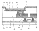
図1(A)に示すように、絶縁表面を有する基板上に下地膜を介して半導体膜100と、第1の絶縁膜(絶縁層)101を形成する。基板には、例えばバリウムホウケイ酸ガラスや、アルミノホウケイ酸ガラスなどのガラス基板、石英基板、半導体基板表面に絶縁膜を形成した基板、金属基板表面に絶縁膜を形成した基板などを用いることができる。また、ポリエチレン-テレフタレート(PET)、ポリエチレンナフタレート(PEN)、ポリエーテルサルフォン(PES)に代表されるプラスチックや、アクリルなどの可撓性を有する合成樹脂からなる基板を用いることができる。
As shown in FIG. 1A, a
半導体膜100は、トランジスタなどの能動素子の主要部を形成するための部材であり、珪素(シリコン)の他に、シリコンゲルマニウム、ガリウム砒素などの化合物半導体であっても良い。また、単結晶に限定されず、非晶質、多結晶、準結晶などの各種半導体を適用することができる。例えば、スパッタ法、LPCVD法、またはプラズマCVD法などにより形成される非晶質半導体膜をレーザー光などの強光で結晶化させた結晶性半導体膜を用いることもできる。
The
第1の絶縁膜101は、半導体膜100に形成される素子と、その素子を連接する配線とを分離する所謂層間絶縁膜として機能させるものである。これは、無機材料(酸化シリコン、窒化シリコン、酸化窒化シリコンなど)、感光性または非感光性の有機材料(ポリイミド、アクリル、ポリアミド、ポリイミドアミド、レジストまたはベンゾシクロブテン)を用いることができる。また、珪素(Si)と酸素(O)との結合で骨格構造が構成され、置換基に少なくとも水素を含む、または置換基にフッ素、アルキル基、または芳香族炭化水素のうち少なくとも1種を有する材料、いわゆるシロキサン結合を有する絶縁膜及びそれらの積層構造を用いることができる。
The first
第1の絶縁膜101を貫通する開孔102は、所謂コンタクトホールと呼ばれるものであり、フォトレジストにより所定のマスクを形成し、該マスクを用いてドライエッチング又はウェットエッチングにより形成することができる。
The
第1の絶縁膜101上には、半導体膜100とオーミックコンタクトを形成するための導電膜(以下、便宜上「コンタクト層」ともいう。)を形成する。第1の絶縁膜101上に形成された第1のコンタクト層103は、開孔102で半導体膜100と接触する。第1のコンタクト層103は、チタン(Ti)、タングステン(W)、タンタル(Ta)窒化タンタル(TaN)、窒化チタン(TiN)又は窒化タングステン(WN)、炭化タンタル(TaC)、炭化チタン(TiC)、その他半導体膜100とオーミックコンタクトを形成することのできる導電性材料で形成する。一例としては、珪素半導体膜に対し10〜45atomic%の窒素を含む窒化チタンを用いることで良好なオーミックコンタクトを形成することができる。また、窒化チタンは、珪素との反応により、その剥離(ピーリングとも呼ばれる。)を抑制する効果もある。その他にもコンタクト層は、アルミニウムや銅など比較的化学的安定性に欠く導電性材料とのコンタクト形成にも適用する。
A conductive film (hereinafter also referred to as a “contact layer” for convenience) for forming an ohmic contact with the
次いで、第1のコンタクト層103上に第1のバリア層104と、第1の導電膜105を形成する。第1のバリア層104は、第1の導電膜105を形成する材料が半導体膜100に拡散することを防止するために設け、窒化タンタル(TaN)、窒化チタン(TiN)又は窒化タングステン(WN)、炭化タンタル(TaC)、炭化チタン(TiC)窒化タングステン(TiW)から選ばれた一種或いは複数種の材料を用いることができる。例えば、ほぼ化学量論的組成に近い窒化チタンを用いれば、アルミニウム若しくはアルミニウムを主成分とする材料で形成する第1の導電膜105からの拡散を防止することができる。
Next, a
第1の導電膜105は、開孔102を埋め込み、かつ、層間絶縁膜に埋め込まれ下層配線と上層配線との間に介装される柱状の導電性部材を形成できる程度の厚さで形成する。第1の導電膜105は、タングステン(W)、アルミニウム(Al)、銅(Cu)及びそれらを主成分とする合金又は化合物を用いることができる。具体的な合金としては、AlにSc、Si、Cu、Ti、Geなどを0.01〜5wt%添加したAl合金、例えばAl−Si合金、Al−Ti合金、Al−Ge合金を用いることができる。また、Ge、Sn、Ga、Zn、Pb、In及びSbなどから選択された元素を含む材料を用いるか、Al膜上に前記の元素を含む薄膜を積層形成することで、加熱処理による流動性の向上やリフローによるコンタクトホールの埋め込みを可能とする熱処理温度の低温化を図ることが好ましい。第1の導電膜105としてスパッタリング法により形成されるAl−Ge合金を用いると、300〜500℃の熱処理によりリフローを行うことができる。
The first
第1の導電膜105上にマスク106を形成し、エッチング加工をして、図1(B)に示すように、柱状の導電性部材107、108を形成する。なお柱状の導電性部材は、コンタクトホールを充填する導電層として形成される。エッチングは、マスク106の位置に柱状の導電性部材107を残存させ、かつ、開孔102を埋め込む導電層108が第1の絶縁膜101若しくは第1のバリア層104と略同一平面を形成するように、第1のバリア層104の上面をエッチングストッパーとして利用している。なお、柱状の導電性部材107を形成する位置は、導電層108が形成される領域外として、第1の絶縁膜101の下層側と上層側に対するコンタクトの形成位置を異ならせている。
A
次に、マスク106を除去して、図1(C)に示すように、柱状の導電性部材107を覆うように第2のコンタクト層109、第2のバリア層110、第2の導電膜111を順次形成する。第2のコンタクト層109は柱状の導電性部材107、導電層108との低接触抵抗のコンタクトを確保するために設け、第2のバリア層110は、第2の導電膜111に含まれるアルミニウム(Al)、銅(Cu)及びそれらを主成分とする合金又は化合物が半導体膜側など周辺に拡散することを抑制するために設けている。第2の導電膜111は、柱状の導電性部材107を十分被覆できる厚さで形成し、その上に第3のバリア層112、第3のコンタクト層113を形成する。
Next, the
その後、第1のコンタクト層103、第1のバリア層104、第2のコンタクト層109、第2のバリア層110、第2の導電膜111、第3のバリア層112、第3のコンタクト層113をエッチングして、第1の絶縁膜101上に下層配線114を形成する。この下層配線114は、柱状の導電性部材107に起因する凸状部が作り込まれることとなる。
After that, the
下層配線114を埋め込む第2の絶縁膜115を形成し、エッチバック又はCMPなどの技術により、表面を平坦化すると共に後退させて凸状部を露出させることで、図2(A)に示すような構造を得る。
As shown in FIG. 2A, a second
第2の絶縁膜115は、無機材料(酸化シリコン、窒化シリコン、酸化窒化シリコンなど)、感光性または非感光性の有機材料(ポリイミド、アクリル、ポリアミド、ポリイミドアミド、レジストまたはベンゾシクロブテン)、珪素(Si)と酸素(O)との結合で骨格構造が構成され、置換基に少なくとも水素、又は置換基にフッ素、アルキル基、または芳香族炭化水素のうち少なくとも一種を有する材料、いわゆるシロキサン、及びそれらの積層構造を用いることができる。有機材料として、ポジ型感光性有機樹脂又はネガ型感光性有機樹脂を用いることができる。
The second
凸状部は、第2の絶縁膜上に形成する上層配線と電気的な接続を形成できる程度に露出していれば良い。従って、第2の絶縁膜の上面と略同一平面で露出していても良いし、一部が突出していても良い。但し、第2の絶縁膜により段差が平坦化される場合、凸状部の段差のみでアライメントマークを形成することになるので、凸状部の作る段差は、アライメントマークの検出に必要な高さがなければならない。 The convex portion only needs to be exposed to such an extent that an electrical connection can be formed with the upper layer wiring formed on the second insulating film. Therefore, it may be exposed in substantially the same plane as the upper surface of the second insulating film, or a part thereof may protrude. However, when the level difference is flattened by the second insulating film, the alignment mark is formed only by the level difference of the convex part. Therefore, the level difference formed by the convex part is a height necessary for detecting the alignment mark. There must be.
図2(B)に示すように、第2の絶縁膜115から露出した下層配線114の凸状部で電気的な接続をとることができるように第4のバリア層116と第3の導電膜117を形成する。これらの層は、同様の目的のために前述したものと同じ材料を用いて形成することができる。
As shown in FIG. 2B, the
その後、マスク118を形成し、第3の導電膜117をエッチングして、図2(C)に示すような柱状の導電性部材119を形成する。柱状の導電性部材119を形成する位置は、柱状の導電性部材107と重ならない位置に形成しているが、重なっていても構わない。このエッチングでは、第4のバリア層116がエッチングストッパーとして機能するため、下地とは選択性良く加工することができる。さらに、全面に形成された第4のバリア層116を残存させることにより、第2の絶縁膜を剥離液に晒すことなくマスク118を剥離することができる。これは、第2の絶縁膜115を有機樹脂系の材料で形成した場合には特に有効である。
After that, a
図3(A)に示すように、柱状の導電性部材107を覆うようにして、第4のコンタクト層120、第5のバリア層121、第4の導電膜122、第6のバリア層123、第5のコンタクト層124、酸化珪素などの無機材料から成るマスク(以下「ハードマスク」ともいう。)125を順次形成する。その後、フォトレジストで上層配線を形成するためのマスク126を形成する。
As shown in FIG. 3A, a
その後、図3(B)に示すように、第4の導電膜122、第6のバリア層123、第5のコンタクト層124、ハードマスク125をエッチングして除去する。このエッチングでも、第4のバリア層116や第5のバリア層121がエッチングストッパーとなり、さらにマスク126を剥離するときに第2の絶縁膜115が剥離液に晒さないための保護膜(保護層)としても機能する。特に、第2の絶縁膜115が有機樹脂系の材料で形成されている場合には、剥離液に晒されて膨潤してしまうことを防ぐことができる。すなわち、マスク除去のために直接剥離液に曝されることがない。そのため、剥離液に曝されたことによる脱水処理や膨潤を回復させるための加熱処理を行う必要がない。また、マスク126を剥離した後に、ハードマスク125があることで、第5のコンタクト層124よりも下層の配線を保護することができる。
After that, as shown in FIG. 3B, the fourth
その後、図4に示すように、ハードマスク125を用いて、第4のバリア層116、第4のコンタクト層120、第5のバリア層121をエッチング除去する。その後、第3の絶縁膜128をハードマスク及び第2の絶縁膜上に形成する。第3の絶縁膜128は第2の絶縁膜115と同様に、エッチバック又はCMPなどの技術により、表面を平坦化すると共に後退させて凸状部を露出させることで、第5のコンタクト層124が露出するような構造とする。第3の絶縁膜128には、無機材料(酸化シリコン、窒化シリコン、酸化窒化シリコンなど)、感光性または非感光性の有機材料(ポリイミド、アクリル、ポリアミド、ポリイミドアミド、レジストまたはベンゾシクロブテン)、珪素(Si)と酸素(O)との結合で骨格構造が構成され、置換基に少なくとも水素を含む、または置換基にフッ素、アルキル基、または芳香族炭化水素のうち少なくとも1種を有する材料、いわゆるシロキサン、及びそれらの積層構造を用いることができる。有機材料として、ポジ型感光性有機樹脂又はネガ型感光性有機樹脂を用いることができる。
Thereafter, as shown in FIG. 4, the
以上のような工程を繰り返すことにより、多層配線構造を形成することができる。この多層配線構造は、解像限界以下のパターン形成が比較的容易に行うことができるので、コンタクト径の微細化を達成することができる。さらに、配線を積層構造とすることにより、配線抵抗を低減することができる。加えて、下層配線と上層配線の間の層間絶縁膜を非常に厚くしたい場合においても、凸状部を有する下層配線を用いれば、凸状部の高さの制御のみで簡便に下層配線と上層配線の導通をとることができる。 By repeating the above steps, a multilayer wiring structure can be formed. In this multilayer wiring structure, pattern formation below the resolution limit can be performed relatively easily, so that the contact diameter can be reduced. Furthermore, the wiring resistance can be reduced by providing the wiring with a laminated structure. In addition, even when it is desired to make the interlayer insulating film between the lower layer wiring and the upper layer wiring very thick, if the lower layer wiring having the convex portion is used, the lower layer wiring and the upper layer can be simply controlled only by controlling the height of the convex portion. Wiring can be conducted.
なお、本実施例では、第1の絶縁膜101にコンタクトホールを形成したが、本発明はこれに限定されず、全ての配線に関し、層間絶縁膜を介して形成される下層配線と上層配線とを電気的に接続するために、下層配線を構成する導電膜を利用して凸状部を形成して、それにより電気的な接続を形成する多層配線構造で形成しても良い。
In this embodiment, the contact hole is formed in the first insulating
このような多層配線構造は、半導体基板に形成されたMOSトタンジスタや絶縁表面上に形成されたTFTで形成された回路を有する半導体装置のみでなく、液晶表示装置や発光素子を各画素に備えた発光装置、DMD(Digital Micro mirror Device)、PDP(Plasma Display Panel)、FED(Field Emission Display)などの画素部及び駆動回路部にも適用することができる。 Such a multilayer wiring structure includes not only a semiconductor device having a circuit formed by a MOS transistor formed on a semiconductor substrate or a TFT formed on an insulating surface, but also a liquid crystal display device and a light emitting element in each pixel. The present invention can also be applied to a pixel unit and a drive circuit unit such as a light emitting device, DMD (Digital Micromirror Device), PDP (Plasma Display Panel), and FED (Field Emission Display).
本実施例は、本発明の配線構造で構成される発光装置の一例について図面を参照して説明する。本実施例で説明する発光装置は、TFTで発光素子の制御を行うものであり、特に、当該TFTと発光素子とを接続する配線に本発明を適用する場合について説明する。 In this example, an example of a light-emitting device including the wiring structure of the present invention will be described with reference to the drawings. The light-emitting device described in this embodiment controls a light-emitting element with a TFT. In particular, a case where the present invention is applied to a wiring connecting the TFT and the light-emitting element will be described.
図5は、絶縁膜201が形成された基板200上にTFT202、第1の絶縁膜203、配線204及び205が形成されている。配線204及び205は、第1の絶縁膜203に形成された開口部(コンタクトホール)206を介してTFT202のソース又はドレイン領域を形成する一導電型の不純物領域に接続している。実施例1と同様に、配線204及び205は、第1のコンタクト層103、第1のバリア層104、柱状の導電性部材107及び導電層108、第2のコンタクト層109、第2のバリア層110、第2の導電膜111、第3のバリア層112、第3のコンタクト層113から構成されている。
In FIG. 5, a
第2の絶縁膜207は、配線204及び205を埋め込む形で形成され、配線204の凸状部の頂部が略同一平面で露出するように形成する。若しくは、第2の絶縁膜207を形成後、表面層をCMPやエッチバック処理により除去して平坦化しつつ凸状部を露出させても良い。
The second
第2の絶縁膜207上には、配線204の露出している凸状部と接するように第1の電極208を形成する。第1の電極208は発光素子の一方の電極を形成するものであり、このような接続構造を形成することにより、平坦な面に第1の電極208を形成することができ、発光素子の有効面積を拡大することができる。
A
そして、第1の電極208を覆うように第3の絶縁膜209を設ける。第3の絶縁膜209は第1の電極208上に開口部を形成する。第1の電極208と接するようにEL層210を設ける。EL層210上には第2の電極211を形成し、これらが第1の電極208と重なる領域で発光素子が形成される。第3の絶縁膜209は、第1の電極208の端部を覆うことにより、この部位での短絡欠陥の発生を防ぎ、隣接する発光素子間を分離している。
Then, a third
EL層210はそのキャリア輸送特性から、正孔輸送層、発光層、電子輸送層を積層させるものである。また、正孔注入電極と正孔輸送層との間に正孔注入層を設けても良いし、電子注入電極と電子輸送層との間に電子注入層を設けても良い。正孔注入層と正孔輸送層、及び電子注入層と電子輸送層との区別は必ずしも厳密なものではなく、これらは正孔輸送性(正孔移動度)及び電子輸送性(電子移動度)が特に重要な特性である意味において同じである。また、電子輸送層と発光層の間に正孔ブロック層を設けた構成としても良い。発光層はホスト材料に顔料や金属錯体などのゲスト材料を添加して、発光色を異ならせた構成としても良い。すなわち、発光層は蛍光物質又は燐光物質を含ませて形成すれば良い。発光層は電子輸送層を兼ねる場合もあり、発光性電子輸送層とも呼ばれる。
The
EL層210の一例としては、正孔注入層としてCuPc若しくはPEDOT、正孔輸送層としてα−NPD、電子輸送層としてBCP若しくはAlq3、電子注入層としてBCP:Li若しくはCaF2を用いることができる。また、発光層としては、赤色、緑色、青色のそれぞれの発光色に対応したドーパント(赤色の場合DCMなど、緑色の場合はDMQDなど)を添加したAlq3を用いればよい。
As an example of the
EL層は有機化合物のみでなく、有機材料と無機材料とを複合化した材料、有機化合物に金属錯体を添加した材料などを用いても、同様な機能を発現するものであれば置換して適用することができる。例えば、正孔注入層に酸化モリブデン(MoOx:x=2〜3)などの酸化物とα−NPDやルブレンを共蒸着した複合材料を用いることができる。 The EL layer is not only an organic compound but also a material that combines an organic material and an inorganic material, or a material in which a metal complex is added to an organic compound. can do. For example, a composite material in which an oxide such as molybdenum oxide (MoOx: x = 2 to 3) and α-NPD or rubrene are co-evaporated can be used for the hole injection layer.
勿論、ELを発現するための層構造には様々なものがあり、特定の正孔注入層や電子輸送層などの代わりに、もっぱらこの目的を奏するための電極を備えたり、同質の効果が得られる材料を分散させて備えたりする変形は、本実施例の趣旨を逸脱しない範囲において許容されうるものである。 Of course, there are various layer structures for developing EL, and instead of a specific hole injection layer or electron transport layer, an electrode for this purpose can be provided, or the same effect can be obtained. Such a modification that the prepared material is dispersed is acceptable within a range not departing from the gist of the present embodiment.
また、多色表示を行う場合、各画素に応じてカラーフィルター又は色変換層などを別途設けることによって色純度の良い表示を行うことができる。 In the case of performing multicolor display, display with good color purity can be performed by separately providing a color filter or a color conversion layer according to each pixel.
第1の電極208及び第2の電極211は、一方が正孔を注入する側の電極(陽極)(以下「正孔注入電極」ともいう。)となり、他方が電子を注入する側の電極(陰極)(以下「電子注入電極」ともいう。)として機能するように形成する材料を選択する。
One of the
第1の電極208(正孔注入電極)としては、仕事関数の大きい(仕事関数4.0eV以上)金属、合金、電気伝導性化合物、およびこれらの混合物などを用いることが好ましい。具体例な材料としては、ITO(indium tin oxide)、酸化インジウムに2〜20%の酸化亜鉛(ZnO)を混合したIZO(indium zinc oxide)、酸化インジウムに2〜20%の酸化珪素(SiO2)を混合した材料(ITSOとも表記する)、金(Au)、白金(Pt)、ニッケル(Ni)、タングステン(W)、クロム(Cr)、モリブデン(Mo)、鉄(Fe)、コバルト(Co)、銅(Cu)、パラジウム(Pd)、または金属材料の窒化物(TiN)などを用いることができる。 As the first electrode 208 (hole injection electrode), a metal, an alloy, an electrically conductive compound, a mixture thereof, or the like having a high work function (work function of 4.0 eV or more) is preferably used. Specific examples include ITO (indium tin oxide), IZO (indium zinc oxide) in which 2 to 20% zinc oxide (ZnO) is mixed with indium oxide, and 2 to 20% silicon oxide (SiO 2 ) in indium oxide. ) Mixed materials (also expressed as ITSO), gold (Au), platinum (Pt), nickel (Ni), tungsten (W), chromium (Cr), molybdenum (Mo), iron (Fe), cobalt (Co ), Copper (Cu), palladium (Pd), or a nitride of metal (TiN) can be used.
第2の電極211(電子注入電極)としては、仕事関数の小さい(仕事関数3.8eV以下)金属、合金、電気伝導性化合物、およびこれらの混合物などを用いることが好ましい。具体的には、元素周期律表の1族または2族に属する元素、すなわちLiやCsなどのアルカリ金属、およびMg、Ca、Srなどのアルカリ土類金属、およびこれらを含む合金(Mg:Ag、Al:Li)や化合物(LiF、CsF、CaF2)の他、希土類金属を含む遷移金属を用いて形成することができる。また、これらの金属又はこれらの金属を含む合金を非常に薄く形成し、ITO、IZO、ITSO又はその他の金属(合金を含む)との積層により形成することができる。 As the second electrode 211 (electron injection electrode), it is preferable to use a metal, an alloy, an electrically conductive compound, a mixture thereof, or the like having a low work function (work function of 3.8 eV or less). Specifically, elements belonging to Group 1 or Group 2 of the Periodic Table of Elements, that is, alkali metals such as Li and Cs, and alkaline earth metals such as Mg, Ca, and Sr, and alloys containing these (Mg: Ag , Al: Li) and compounds (LiF, CsF, CaF 2 ), as well as transition metals including rare earth metals. Further, these metals or alloys containing these metals can be formed very thinly, and can be formed by stacking with ITO, IZO, ITSO, or other metals (including alloys).
このように、発光素子213は第1の電極208と第2の電極211との間にEL層210を挟み込む形で構成される。
As described above, the light-emitting
勿論、正孔注入電極として機能する第1の電極と、電子注入電極として機能する第2の電極とは、EL層と相対的な関係にあるので、EL層の積層構造に応じて、第1の電極を電子注入電極、第2の電極を正孔注入電極として上記の材料を用いて形成しても良い。 Of course, since the first electrode functioning as a hole injection electrode and the second electrode functioning as an electron injection electrode are in a relative relationship with the EL layer, the first electrode depends on the stacked structure of the EL layer. These electrodes may be formed using the above materials as an electron injection electrode and a second electrode as a hole injection electrode.
第2の電極211上には、保護膜212を設けても良い。保護膜212は、プラズマCVD法やスパッタリング法などにより窒化珪素などの絶縁層で形成する。勿論、保護膜212は、水蒸気など外因性の不純物の侵入を防止できるバリア性のある絶縁層であれば他のものを適用することができ、窒化炭素やダイヤモンドライクカーボンなどの材料で形成することができる。また、ガスバリア性を高め、さらに保護膜による応力の影響を低減する構造として、バリア性の絶縁層と吸湿性の絶縁層とを交互に積層した多層構造としても良い。
A
以上のように、TFT202と発光素子213との接続に、柱状の導電性部材を埋め込んで形成した凸状部を有する配線を用いた発光装置が得られる。
As described above, a light-emitting device using a wiring having a convex portion formed by embedding a columnar conductive member in the connection between the
図6は同様に、逆スタガ型TFT302と発光素子213を柱状の導電性部材を埋め込んで形成した凸状部を有する配線を用いた発光装置の一例を示している。逆スタガ型TFT302は、ゲート電極、ゲート絶縁膜、チャネル形成領域、ソース及びドレインを形成する半導体膜を順次積層した構造を有している。配線204、205は、第1の絶縁膜203に形成されたコンタクトホール206によって逆スタガ型TFT302と接続している。この接続構造は、図5で説明したものと同様である。
Similarly, FIG. 6 shows an example of a light-emitting device using a wiring having a convex portion formed by embedding a columnar conductive member in the inverted staggered
なお、本実施例では、第1の絶縁膜を介してTFTと発光素子の一方の電極とを、本発明の多層配線構造を適用して接続する構成について例示したが、本発明はこれに限定されず、複数の絶縁層を介して下層配線と上層配線とを電気的に接続した構造を持った発光装置とすることもできる。 In this embodiment, the configuration in which the TFT and one electrode of the light emitting element are connected through the first insulating film by applying the multilayer wiring structure of the present invention is described. However, the present invention is not limited to this. Alternatively, a light emitting device having a structure in which a lower layer wiring and an upper layer wiring are electrically connected through a plurality of insulating layers can be provided.
図9〜図12は実施例2で示す発光素子の詳細な構成を説明する図であり、以下に示す発光素子を実施例2の発光素子として適用して発光装置を構成することができる。 9 to 12 are diagrams illustrating a detailed configuration of the light-emitting element shown in Example 2. A light-emitting device can be configured by applying the light-emitting element shown below as the light-emitting element of Example 2. FIG.
図9(A)は第1の電極11を透光性の酸化物導電性材料で形成した例であり、ITOなどの酸化物導電性材料若しくは酸化珪素を含む酸化物導電性材料で形成している。その上に正孔注入層若しくは正孔輸送層41、発光層42、電子輸送層若しくは電子注入層43を積層したEL層16を設けている。第2の電極17は、LiFやMgAgなどアルカリ金属又はアルカリ土類金属を含む第3の電極層33とアルミニウムなどの金属材料で形成する第4の電極層34で形成している。この構造の画素は、図中に矢印で示したように第1の電極11側から光を放射することが可能となる。
FIG. 9A illustrates an example in which the
図9(B)は第2の電極17から光を放射する例を示し、第1の電極11はアルミニウム、チタンなどの金属、又は該金属と化学量論的組成比以下の濃度で窒素を含む金属材料で形成する第1の電極層31と、酸化珪素を1〜15原子%の濃度で含む酸化物導電性材料で形成する第2の電極層32で形成している。その上に正孔注入層若しくは正孔輸送層41、発光層42、電子輸送層若しくは電子注入層43を積層したEL層16を設けている。第2の電極17は、LiFやCaFなどのアルカリ金属又はアルカリ土類金属を含む第3の電極層33とアルミニウムなどの金属材料で形成する第4の電極層34で形成するが、いずれの層も100nm以下の厚さとして光を透過可能な状態としておくことで、第2の電極17から光を放射することが可能となる。
FIG. 9B shows an example in which light is emitted from the
図10(A)は第1の電極11から光を放射する例を示し、かつ、EL層を電子輸送層若しくは電子注入層43、発光層42、正孔注入層若しくは正孔輸送層41の順に積層した構成を示している。第2の電極17は、EL層16側から酸化珪素を1〜15原子%の濃度で含む酸化物導電性材料で形成する第2の電極層32、アルミニウム、チタンなどの金属、又は該金属と化学量論的組成比以下の濃度で窒素を含む金属材料で形成する第1の電極層35で形成している。第1の電極11は、LiFやCaFなどのアルカリ金属又はアルカリ土類金属を含む第3の電極層33とアルミニウムなどの金属材料で形成する第4の電極層34で形成するが、いずれの層も100nm以下の厚さとして光を透過可能な状態としておくことで、第1の電極11から光を放射することが可能となる。
FIG. 10A shows an example in which light is emitted from the
図10(B)は第2の電極17から光を放射する例を示し、かつ、EL層16を電子輸送層若しくは電子注入層43、発光層42、正孔注入層若しくは正孔輸送層41の順に積層した構成を示している。第1の電極11は図10(A)と同様な構成とし、膜厚はEL層16で発光した光を反射可能な程度に厚く形成している。第2の電極17は、ITOなどの酸化物導電性材料若しくは酸化珪素を含む酸化物導電性材料で形成している。この構造において、正孔注入層を無機物である金属酸化物(代表的には酸化モリブデン若しくは酸化バナジウム)で形成することにより、第2の電極層32を形成する際に導入される酸素が供給されて正孔注入性が向上し、駆動電圧を低下させることができる。
FIG. 10B shows an example in which light is emitted from the
図11と図12は、第1の電極11及び第2の電極17の両側から光を放射することができる構成の画素を示している。
FIGS. 11 and 12 show a pixel having a structure capable of emitting light from both sides of the
図11(A)は、第1の電極11を透光性の酸化物導電性材料で形成した例であり、ITOなどの酸化物導電性材料若しくは酸化珪素を含む酸化物導電性材料で形成しする。その上に正孔注入層若しくは正孔輸送層41、発光層42、電子輸送層若しくは電子注入層43を積層したEL層16を設けている。第2の電極17は、LiFやCaFなどのアルカリ金属又はアルカリ土類金属を含む第3の電極層33とアルミニウムなどの金属材料で形成する第4の電極層34で形成するが、いずれの層も100nm以下の厚さとして光を透過可能な状態としておくことで、第2の電極17と第1の電極11の両方から光を放射することが可能となる。
FIG. 11A illustrates an example in which the
図11(B)は、第1の電極をLiFやCaFなどのアルカリ金属又はアルカリ土類金属を含む第3の電極層33とアルミニウムなどの金属材料で形成する第4の電極層34で形成するが、いずれの層も100nm以下の厚さとして光を透過可能な状態としておく。この上にEL層16を、電子輸送層若しくは電子注入層43、発光層42、正孔注入層若しくは正孔輸送層41の順に積層している。第2の電極17は、ITOなどの酸化物導電性材料若しくは酸化珪素を含む酸化物導電性材料で形成している。このような構成としても、第2の電極17と第1の電極11の両方から光を放射することが可能となる。
In FIG. 11B, the first electrode is formed of a
図12(A)と(B)は、第1の電極11と第2の電極17を共に同様な材料で形成したものであり、すなわち、酸化物導電性材料で第1の電極11と第2の電極17の両方を形成したものであり、ITOなどの酸化物導電性材料若しくは酸化珪素を含む酸化物導電性材料で形成している。このとき、EL層16の正孔注入層若しくは正孔輸送層41の第2の電極層32側の層を金属酸化物(代表的には酸化モリブデン若しくは酸化バナジウム)で形成し、電子輸送層若しくは電子注入層43の第3の電極層33側の層を、アルカリ金属又はアルカリ土類金属を含む有機物(代表的にはベンゾオキサゾール誘導体、ピリジン誘導体)で形成すると良い。
12A and 12B show that the
本実施例は、本発明の配線構造で構成される液晶表示装置の一例について図面を参照して説明する。本実施例で説明する液晶表示装置は、TFTで液晶の制御を行うものであり、特に、当該TFTと液晶の配向を制御する電極とを接続する配線に本発明を適用する場合について説明する。 In this embodiment, an example of a liquid crystal display device having the wiring structure of the present invention will be described with reference to the drawings. The liquid crystal display device described in this embodiment controls a liquid crystal by using a TFT. In particular, a case where the present invention is applied to a wiring connecting the TFT and an electrode for controlling the alignment of the liquid crystal will be described.
図7は、基板200上に逆スタガ型TFT302、第1の絶縁膜203、配線204及び205が形成されている。配線204及び205は、第1の絶縁膜203に形成された開口部206を介してTFT302のソース又はドレイン領域を形成する一導電型の不純物領域に接続している。実施例2と同様に、配線204及び205は、第1のコンタクト層103、第1のバリア層104、凸状部107及び108、第2のコンタクト層109、第2のバリア層110、第2の導電膜111、第3のバリア層112、第3のコンタクト層113から構成されている。
In FIG. 7, an inverted
第2の絶縁膜207は、配線204及び205を埋め込む形で形成され、配線204の凸状部の頂部が略同一平面で露出するように形成する。若しくは、第2の絶縁膜207を形成後、表面層をCMPやエッチバック処理により除去して平坦化しつつ凸状部を露出させても良い。
The second
第2の絶縁膜207上には、配線204の露出している凸状部と接するように第1の電極401を形成する。第1の電極401は発光素子の一方の電極を形成するものであり、このような接続構造を形成することにより、平坦な面に第1の電極401を形成することができ、画素電極の有効面積を拡大することができ、ディスクリネーションを防止することができる。
On the second
対向基板400には、遮光層403、着色層404、アクリル材などで形成される平坦化層405、対向電極406が形成されている。対向基板400と基板200とは、スペーサ(図示しない)を介して固着されその間に液晶407が封入されている。
The
第1の電極401及び第2の電極(対向電極に相当)406の両者を透光性の導電膜で形成すると透過型の液晶表示装置とすることができ、一方を光反射性の導電膜で形成することで、反射型の液晶表示装置とすることができる。勿論、一方の電極を光反射性の電極として、光透過用の窓部を形成することにより半透過型としても良い。
When both the
実施例1で示した多層配線構造は半導体集積回路の配線に適用することができる。半導体集積回路としては、メモリー、各種プロセッサをはじめ、中央処理装置(以下「CPU」ともいう。)など様々な集積回路が含まれる。 The multilayer wiring structure shown in Embodiment 1 can be applied to the wiring of a semiconductor integrated circuit. The semiconductor integrated circuit includes various integrated circuits such as a memory, various processors, and a central processing unit (hereinafter also referred to as “CPU”).
図8はCPUの一例を示している。基板600上に、演算回路(ALU:Arithmetic logic unit)601、演算回路用の制御部(ALU Controller)602、命令解析部(Instruction Decoder)603、割り込み制御部(Interrupt Controller)604、タイミング制御部(Timing Controller)605、レジスタ(Register)606、レジスタ制御部(Register Controller)607、バスインターフェース(Bus I/F)608、書き換え可能なROM609、ROMインターフェース(ROM I/F)620が配設されている。ROM609及びROMインターフェース(ROM I/F)620は別体としても良い。
FIG. 8 shows an example of the CPU. An arithmetic circuit (ALU) 601, an arithmetic circuit control unit (ALU Controller) 602, an instruction analysis unit (Instruction Decoder) 603, an interrupt control unit (Interrupt Controller) 604, a timing control unit (on the substrate 600) A
バスインターフェース608を介してCPUに入力された命令は、命令解析部603に入力され、デコードされた後、演算回路用の制御部602、割り込み制御部604、レジスタ制御部607、タイミング制御部605に入力される。
An instruction input to the CPU via the
演算回路用の制御部602、割り込み制御部604、レジスタ制御部607、タイミング制御部605は、デコードされた命令に基づき、各種制御を行う。具体的に演算回路用の制御部602は、演算回路601の動作を制御するための信号を生成する。また、割り込み制御部604は、CPUのプログラム実行中に、外部の入出力装置や、周辺回路からの割り込み要求を、その優先度やマスク状態から判断し、処理する。レジスタ制御部607は、レジスタ606のアドレスを生成し、CPUの状態に応じてレジスタ606の読み出しや書き込みを行う。
An arithmetic
またタイミング制御部605は、演算回路601、演算回路用の制御部602、命令解析部603、割り込み制御部604、レジスタ制御部607の動作のタイミングを制御する信号を生成する。例えばタイミング制御部605は、基準クロック信号CLK1(621)を元に、内部クロック信号CLK2(622)を生成する内部クロック生成部を備えており、クロック信号CLK2を上記各種回路に供給する。
The
勿論、図8に示すCPUは、その構成を簡略化して示した一例にすぎず、実際のCPUはその用途によって多種多様な構成を有している。このようなCPUはパッケージングされ、外部から保護され、さらに携帯しやすくなる。そして所望箇所に、CPUを実装することができフレキシブル性を有するように形成すると、実装する位置の自由度が高まる。またパッケージングすることによりCPUの機能を補助することもできる。 Needless to say, the CPU illustrated in FIG. 8 is just an example in which the configuration is simplified, and an actual CPU may have various configurations depending on the application. Such a CPU is packaged, protected from the outside, and easier to carry. If the CPU can be mounted at a desired location and formed so as to have flexibility, the degree of freedom of the mounting position is increased. Further, the function of the CPU can be assisted by packaging.
以上のように、ガラス基板上の薄膜トランジスタにより形成されるCPUは、多様な形態をとることができる。そして、ガラス基板上の薄膜トランジスタにより形成されるCPUは軽量であるため、携帯や実装するときの負担を軽減することができる。 As described above, a CPU formed using thin film transistors over a glass substrate can take a variety of forms. And since CPU formed with the thin-film transistor on a glass substrate is lightweight, the burden at the time of carrying or mounting can be reduced.
このようなCPUは単結晶半導体基板を用いて形成することができるが、その他にもTFTを用いてガラス基板上に形成することができる。特に、ガラス基板上にCPUなどの集積回路を形成する場合には、基板の平坦性の違いにより単結晶半導体基板を用いるよりも微細化が難しくなる。この場合にコンタクトホールパターンに代えて、解像限界以下のパターン形成が比較的容易に行うことができる本発明の多層配線構造を適用すれば、コンタクトの微細化を達成することができる。さらに本発明の多層配線構造は、微細化に有利な点に加えて、配線遅延の低減を目的として層間絶縁膜の膜厚を厚くしたい場合にも、凸状部の高さを制御するのみで容易に多層配線間のコンタクトと取れるという特徴を有している。 Such a CPU can be formed using a single crystal semiconductor substrate, but can also be formed over a glass substrate using a TFT. In particular, when an integrated circuit such as a CPU is formed over a glass substrate, miniaturization is more difficult than when a single crystal semiconductor substrate is used due to the difference in flatness of the substrate. In this case, contact miniaturization can be achieved by applying the multilayer wiring structure of the present invention in which the pattern formation below the resolution limit can be performed relatively easily instead of the contact hole pattern. Furthermore, the multilayer wiring structure of the present invention only has an advantage in miniaturization, and also controls the height of the convex portion when it is desired to increase the thickness of the interlayer insulating film for the purpose of reducing wiring delay. It has a feature that it can be easily contacted between multilayer wirings.
本発明は、図13に例示するテレビ受像機、コンピュータ、映像再生装置、その他の電子装置を完成させることができる。 The present invention can complete a television receiver, a computer, a video reproduction device, and other electronic devices illustrated in FIG.
図13(A)は本発明を適用してテレビ受像機を完成させる一例であり、筐体2001、支持台2002、表示部2003、スピーカー部2004、ビデオ入力端子2005などにより構成されている。例えば、実施例3の発光装置又は実施例4の液晶表示装置は、テレビ受像機として機能を特化することで高精細な画像を表示することができる。
FIG. 13A illustrates an example in which the present invention is applied to complete a television receiver, which includes a
図13(B)は本発明を適用してノート型のパーソナルコンピュータを完成させた一例であり、本体2201、筐体2202、表示部2203、キーボード2204、外部接続ポート2205、ポインティングマウス2206などにより構成されている。例えば、実施例3の発光装置又は実施例4の液晶表示装置は、表示部2203に適用することが可能であり、実施例5によりパーソナルコンピュータの中核部であるCPUを安価で製造でき、前述の表示装置と一体形成することで、薄型のノート型のパーソナルコンピュータを製造することができる。
FIG. 13B is an example in which a laptop personal computer is completed by applying the present invention, which includes a
図13(C)は本発明を適用して映像再生装置を完成させた一例であり、本体2401、筐体2402、表示部A2403、表示部B2404、記録媒体読込部2405、操作キー2406、スピーカー部2407などにより構成されている。実施例3の発光装置又は実施例4の液晶表示装置は、表示部A2403、表示部B2404に適用することが可能であり、実施例5によりCPUを安価で製造でき、前述の表示装置と一体形成することで、薄型の映像再生装置を製造することができる。
FIG. 13C is an example in which the present invention is applied to complete a video reproduction device, which includes a
100 半導体膜
101、203 第1の絶縁膜
103 第1のコンタクト層
104 第1のバリア層
105 第1の導電膜
107、108、119 プラグ
109 第2のコンタクト層
110 第2のバリア層
111 第2の導電膜
112 第3のバリア層
113 第3のコンタクト層
115、207 第2の絶縁膜
116 第4のバリア層
117 第3の導電膜
120 第4のコンタクト層
121 第5のバリア層
122 第4の導電膜
123 第6のバリア層
124 第5のコンタクト層
125 ハードマスク
126 ハードマスク
202 TFT
204、205 配線
208 第1の電極
209 第3の絶縁膜
210 EL層
211 第2の電極
212 保護膜
213 発光素子
100
204, 205
Claims (7)
前記第1の絶縁膜上に、第1の導電膜を形成し、
前記第1の導電膜上に第1のマスクを形成し、
前記第1のマスクを用いて、前記第1の導電膜の少なくとも一部が前記第1の絶縁膜を覆い、且つ、前記第1のマスクを形成した位置に柱状の導電性部材が形成されるようにエッチング処理を行い、
前記第1のマスクを除去し、
前記柱状の導電性部材を覆って第2の導電膜を形成し、
前記第2の導電膜上に、無機材料を用いて第2の絶縁膜を形成し、
前記第2の絶縁膜上に第2のマスクを形成し、
前記第2のマスクを用いて、前記第1の導電膜又は前記第2の導電膜の少なくとも一部が前記第1の絶縁膜を覆うように、少なくとも前記第2の絶縁膜のエッチング処理を行い、
前記第2のマスクを除去し、
前記第2の絶縁膜をマスクとして、前記第1の導電膜、又は、前記第1の導電膜及び前記第2の導電膜のエッチング処理を行い、前記柱状の導電性部材を含む配線を形成することを特徴とする半導体装置の作製方法。 Forming a first insulating film using an organic material;
Forming a first conductive film on the first insulating film;
Forming a first mask on the first conductive film;
Using the first mask, at least a part of the first conductive film covers the first insulating film, and a columnar conductive member is formed at a position where the first mask is formed. So that the etching process
Removing the first mask;
Forming a second conductive film covering the columnar conductive member ;
Forming a second insulating film on the second conductive film using an inorganic material;
Forming a second mask on the second insulating film;
Using the second mask , at least the second insulating film is etched so that at least part of the first conductive film or the second conductive film covers the first insulating film. ,
Removing the second mask;
Using the second insulating film as a mask, the first conductive film or the first conductive film and the second conductive film are etched to form a wiring including the columnar conductive member. A method for manufacturing a semiconductor device.
前記第1の導電膜は、チタン、タンタル、タングステンから選ばれた高融点金属、又は該高融点金属の窒化物から選ばれた一種でなる層と、アルミニウム、又はアルミニウムを主成分とする金属材料でなる層と、を含んで形成し、
前記第2の導電膜は、チタン、タンタル、タングステンから選ばれた高融点金属、又は該高融点金属の窒化物から選ばれた一種でなる層を含んで形成することを特徴とする半導体装置の作製方法。 In claim 1 ,
It said first conductive film, the main component and titanium, tantalum, refractory metals selected from tungsten, or a layer made of one selected from a nitride of the refractory metal, A aluminum, or aluminum And a layer made of a metal material to be formed,
The second conductive film is formed to include a layer made of one kind selected from a refractory metal selected from titanium, tantalum, and tungsten, or a nitride of the refractory metal . Manufacturing method.
前記第1の導電膜は、窒化タンタル、窒化チタン、窒化タングステン、炭化タンタル、炭化チタン、又は窒化タングステンから選ばれた一種若しくは複数種でなる層と、タングステン、アルミニウム、銅又はそれらを主成分とする合金若しくは化合物でなる層と、を含んで形成し、The first conductive film includes one or a plurality of layers selected from tantalum nitride, titanium nitride, tungsten nitride, tantalum carbide, titanium carbide, or tungsten nitride, and tungsten, aluminum, copper, or a main component thereof. And a layer made of an alloy or compound to be formed,
前記第2の導電膜は、チタン、タングステン、タンタル、窒化タンタル、窒化チタン、窒化タングステン、炭化タンタル、又は炭化チタンから選ばれた一種でなる層と、窒化タンタル、窒化チタン、窒化タングステン、炭化タンタル、炭化チタン、又は窒化タングステンから選ばれた一種若しくは複数種でなる層と、タングステン、アルミニウム、銅又はそれらを主成分とする合金若しくは化合物でなる層と、を含んで形成することを特徴とする半導体装置の作製方法。The second conductive film includes a layer selected from titanium, tungsten, tantalum, tantalum nitride, titanium nitride, tungsten nitride, tantalum carbide, or titanium carbide, and tantalum nitride, titanium nitride, tungsten nitride, tantalum carbide. And a layer made of one or more selected from titanium carbide or tungsten nitride and a layer made of tungsten, aluminum, copper, or an alloy or compound containing them as a main component. A method for manufacturing a semiconductor device.
前記第1の絶縁膜上に、第1の導電膜を形成し、
前記第1の絶縁膜における前記コンタクトホールによる凹部を、前記第1の導電膜が充填するように加熱処理を行い、
前記第1の導電膜上に第1のマスクを形成し、
前記第1のマスクを用いて、前記コンタクトホール内に前記第1の導電膜が残存し、且つ、前記第1のマスクを形成した位置に第1の柱状の導電性部材が形成されるようにエッチング処理を行い、
前記第1のマスクを除去し、
前記第1の柱状の導電性部材を覆って第2の導電膜を形成し、
前記第2の導電膜上に第2のマスクを形成し、
前記第2のマスクを用いて、前記第1の導電膜及び前記第2の導電膜をエッチング処理して、前記第1の柱状の導電性部材を含む第1の配線を形成し、
有機材料を用いて、前記第1の配線を埋め込む第2の絶縁膜を形成し、
前記第2の絶縁膜を加工して、前記第1の配線の一部を露出させ、
前記第2の絶縁膜上に、前記第1の配線と電気的に接続する第3の導電膜を形成し、
前記第3の導電膜上に第3のマスクを形成し、
前記第3のマスクを用いて、前記第3の導電膜の少なくとも一部が前記第2の絶縁膜を覆い、且つ、前記第3のマスクを形成した位置に第2の柱状の導電性部材が形成されるようにエッチング処理を行い、
前記第3のマスクを除去し、
前記第2の柱状の導電性部材を覆って第4の導電膜を形成し、
前記第4の導電膜上に、無機材料を用いて第3の絶縁膜を形成し、
前記第3の絶縁膜上に第4のマスクを形成し、
前記第4のマスクを用いて、前記第3の導電膜又は前記第4の導電膜の少なくとも一部が前記第2の絶縁膜を覆うように、少なくとも前記第4の絶縁膜のエッチング処理を行い、
前記第4のマスクを除去し、
前記第4の絶縁膜をマスクとして、前記第4の導電膜、又は、前記第3の導電膜及び前記第4の導電膜のエッチング処理を行い、前記第2の柱状の導電性部材を含む第2の配線を形成することを特徴とする半導体装置の作製方法。 A contact hole is formed in the first insulating film,
Forming a first conductive film on the first insulating film ;
Heat treatment is performed so that the first conductive film fills the recesses formed by the contact holes in the first insulating film,
Forming a first mask on the first conductive film;
Using the first mask, the first conductive film remains in the contact hole, and a first columnar conductive member is formed at the position where the first mask is formed. Etching process
Removing the first mask;
The second conductive film is formed to cover the first columnar conductive member,
Forming a second mask on the second conductive film;
Etching the first conductive film and the second conductive film using the second mask to form a first wiring including the first columnar conductive member,
Forming a second insulating film for embedding the first wiring using an organic material;
Processing the second insulating film to expose a portion of the first wiring;
Forming a third conductive film electrically connected to the first wiring on the second insulating film;
Forming a third mask on the third conductive film;
Using the third mask, at least a part of the third conductive film covers the second insulating film, and a second columnar conductive member is formed at the position where the third mask is formed. Etching process to form,
Removing the third mask;
Forming a fourth conductive film covering the second columnar conductive member;
Forming a third insulating film on the fourth conductive film using an inorganic material;
Forming a fourth mask on the third insulating film;
Using the fourth mask, at least the fourth insulating film is etched so that at least part of the third conductive film or the fourth conductive film covers the second insulating film. ,
Removing the fourth mask;
Using the fourth insulating film as a mask, the fourth conductive film, or the third conductive film and the fourth conductive film are etched to include a second columnar conductive member. A method for manufacturing a semiconductor device, comprising forming two wirings.
前記第1の導電膜は、チタン、タンタル、タングステンから選ばれた高融点金属、又は該高融点金属の窒化物から選ばれた一種でなる層と、アルミニウム、又はアルミニウムを主成分とする金属材料でなる層と、を含んで形成し、 The first conductive film includes a layer made of a refractory metal selected from titanium, tantalum, and tungsten, or a layer selected from nitrides of the refractory metal, and aluminum or a metal material containing aluminum as a main component. And a layer comprising:
前記第2の導電膜は、チタン、タンタル、タングステンから選ばれた高融点金属、又は該高融点金属の窒化物から選ばれた一種でなる層を含んで形成することを特徴とする半導体装置の作製方法。 The second conductive film is formed to include a layer made of one kind selected from a refractory metal selected from titanium, tantalum, and tungsten, or a nitride of the refractory metal. Manufacturing method.
前記第3の導電膜は、チタン、タンタル、タングステンから選ばれた高融点金属、又は該高融点金属の窒化物から選ばれた一種でなる層と、アルミニウム、又はアルミニウムを主成分とする金属材料でなる層と、を含んで形成し、 The third conductive film includes a layer made of a refractory metal selected from titanium, tantalum, and tungsten, or a layer selected from nitrides of the refractory metal, and aluminum or a metal material containing aluminum as a main component. And a layer comprising:
前記第4の導電膜は、チタン、タンタル、タングステンから選ばれた高融点金属、又は該高融点金属の窒化物から選ばれた一種でなる層を含んで形成することを特徴とする半導体装置の作製方法。 The fourth conductive film is formed to include a layer made of a refractory metal selected from titanium, tantalum, and tungsten, or a layer selected from a nitride of the refractory metal. Manufacturing method.
前記第1の導電膜、前記第2の導電膜、及び前記第4の導電膜は、チタン、タングステン、タンタル、窒化タンタル、窒化チタン、窒化タングステン、炭化タンタル、又は炭化チタンから選ばれた一種でなる層と、窒化タンタル、窒化チタン、窒化タングステン、炭化タンタル、炭化チタン、又は窒化タングステンから選ばれた一種若しくは複数種でなる層と、タングステン、アルミニウム、銅又はそれらを主成分とする合金若しくは化合物でなる層と、を含んで形成し、 The first conductive film, the second conductive film, and the fourth conductive film are one selected from titanium, tungsten, tantalum, tantalum nitride, titanium nitride, tungsten nitride, tantalum carbide, or titanium carbide. A layer composed of one or more selected from tantalum nitride, titanium nitride, tungsten nitride, tantalum carbide, titanium carbide, or tungsten nitride, and tungsten, aluminum, copper, or an alloy or compound containing them as a main component And a layer comprising:
前記第3の導電膜は、窒化タンタル、窒化チタン、窒化タングステン、炭化タンタル、炭化チタン、又は窒化タングステンから選ばれた一種若しくは複数種でなる層と、タングステン、アルミニウム、銅又はそれらを主成分とする合金若しくは化合物でなる層と、を含んで形成することを特徴とする半導体装置の作製方法。 The third conductive film includes one or more layers selected from tantalum nitride, titanium nitride, tungsten nitride, tantalum carbide, titanium carbide, or tungsten nitride, and tungsten, aluminum, copper, or a main component thereof. And a layer made of an alloy or a compound to be formed.
Priority Applications (1)
| Application Number | Priority Date | Filing Date | Title |
|---|---|---|---|
| JP2004311126A JP4748967B2 (en) | 2003-11-04 | 2004-10-26 | Method for manufacturing semiconductor device |
Applications Claiming Priority (3)
| Application Number | Priority Date | Filing Date | Title |
|---|---|---|---|
| JP2003375038 | 2003-11-04 | ||
| JP2003375038 | 2003-11-04 | ||
| JP2004311126A JP4748967B2 (en) | 2003-11-04 | 2004-10-26 | Method for manufacturing semiconductor device |
Publications (3)
| Publication Number | Publication Date |
|---|---|
| JP2005159326A JP2005159326A (en) | 2005-06-16 |
| JP2005159326A5 JP2005159326A5 (en) | 2007-08-16 |
| JP4748967B2 true JP4748967B2 (en) | 2011-08-17 |
Family
ID=34741376
Family Applications (1)
| Application Number | Title | Priority Date | Filing Date |
|---|---|---|---|
| JP2004311126A Expired - Fee Related JP4748967B2 (en) | 2003-11-04 | 2004-10-26 | Method for manufacturing semiconductor device |
Country Status (1)
| Country | Link |
|---|---|
| JP (1) | JP4748967B2 (en) |
Families Citing this family (7)
| Publication number | Priority date | Publication date | Assignee | Title |
|---|---|---|---|---|
| EP1760798B1 (en) * | 2005-08-31 | 2012-01-11 | Semiconductor Energy Laboratory Co., Ltd. | Semiconductor device and manufacturing method thereof |
| EP3229066A1 (en) | 2005-12-05 | 2017-10-11 | Semiconductor Energy Laboratory Co., Ltd. | Transflective liquid crystal display with a horizontal electric field configuration |
| CN102646698B (en) * | 2007-09-14 | 2015-09-16 | 株式会社半导体能源研究所 | Semiconductor device and electronic equipment |
| JP2009224238A (en) * | 2008-03-18 | 2009-10-01 | Toppan Printing Co Ltd | Organic electroluminescent element and method of manufacturing the same |
| JP5429454B2 (en) * | 2009-04-17 | 2014-02-26 | ソニー株式会社 | Thin film transistor manufacturing method and thin film transistor |
| WO2011043194A1 (en) | 2009-10-09 | 2011-04-14 | Semiconductor Energy Laboratory Co., Ltd. | Semiconductor device and method for manufacturing the same |
| JP7235418B2 (en) * | 2018-05-18 | 2023-03-08 | 株式会社半導体エネルギー研究所 | Manufacturing method of semiconductor device |
Family Cites Families (5)
| Publication number | Priority date | Publication date | Assignee | Title |
|---|---|---|---|---|
| JPH07109828B2 (en) * | 1988-09-14 | 1995-11-22 | 日本電気株式会社 | Method for manufacturing multilayer wiring structure |
| JPH08181213A (en) * | 1994-12-27 | 1996-07-12 | Kawasaki Steel Corp | Manufacture of semiconductor device |
| JPH08274164A (en) * | 1995-03-31 | 1996-10-18 | Seiko Epson Corp | Semiconductor device |
| JPH08306779A (en) * | 1995-05-10 | 1996-11-22 | Sony Corp | Fabrication of semiconductor device |
| JP2000012683A (en) * | 1998-06-17 | 2000-01-14 | Nec Corp | Integrated circuit and manufacture thereof |
-
2004
- 2004-10-26 JP JP2004311126A patent/JP4748967B2/en not_active Expired - Fee Related
Also Published As
| Publication number | Publication date |
|---|---|
| JP2005159326A (en) | 2005-06-16 |
Similar Documents
| Publication | Publication Date | Title |
|---|---|---|
| US7524709B2 (en) | Manufacturing method for a display device | |
| JP7216862B2 (en) | light emitting device | |
| JP4519532B2 (en) | LIGHT EMITTING DEVICE AND ELECTRONIC DEVICE USING LIGHT EMITTING DEVICE | |
| US7663311B2 (en) | Organic light emitting display (OLED) device and method of fabricating the same | |
| EP1511081B1 (en) | Light emitting device | |
| JP6136578B2 (en) | DISPLAY DEVICE, DISPLAY DEVICE MANUFACTURING METHOD, AND ELECTRONIC DEVICE | |
| TWI434608B (en) | Display unit | |
| US6891270B2 (en) | Semiconductor device and method of manufacturing the same | |
| JP2002258325A (en) | Thin film transistor liquid crystal display device | |
| US9547252B2 (en) | Organic light emitting device | |
| TWI611613B (en) | Organic light emitting device and method of manufacturing the device | |
| CN104952903A (en) | Display device, method of manufacturing the same, and method of repairing the same | |
| US9190430B2 (en) | Method of fabricating display panel | |
| US7524734B2 (en) | Wiring substrate, electro-optic device, electric apparatus, method of manufacturing wiring substrate, method of manufacturing electro-optic device, and method of manufacturing electric apparatus | |
| JP5174322B2 (en) | Manufacturing method of active matrix display device | |
| JP3420145B2 (en) | Method for manufacturing semiconductor integrated circuit device | |
| JP4748967B2 (en) | Method for manufacturing semiconductor device | |
| US9923039B2 (en) | Display panels, methods of manufacturing the same and organic light emitting display devices having the same | |
| JP2017162832A (en) | Display device and electronic apparatus | |
| KR100623253B1 (en) | Method of fabricating OLED | |
| WO2023052894A1 (en) | Display device, display module, electronic apparatus, and method for manufacturing display device | |
| JP7464541B2 (en) | Display backplate and manufacturing method thereof, display panel and manufacturing method thereof, display device | |
| US7838884B2 (en) | Display device and fabrication method of display device | |
| KR20110113041A (en) | Array substrate for organic electroluminescent device and method of fabricating the same |
Legal Events
| Date | Code | Title | Description |
|---|---|---|---|
| A521 | Request for written amendment filed |
Free format text: JAPANESE INTERMEDIATE CODE: A523 Effective date: 20070704 |
|
| A621 | Written request for application examination |
Free format text: JAPANESE INTERMEDIATE CODE: A621 Effective date: 20070704 |
|
| A977 | Report on retrieval |
Free format text: JAPANESE INTERMEDIATE CODE: A971007 Effective date: 20090622 |
|
| A131 | Notification of reasons for refusal |
Free format text: JAPANESE INTERMEDIATE CODE: A131 Effective date: 20101019 |
|
| A521 | Request for written amendment filed |
Free format text: JAPANESE INTERMEDIATE CODE: A523 Effective date: 20101216 |
|
| A01 | Written decision to grant a patent or to grant a registration (utility model) |
Free format text: JAPANESE INTERMEDIATE CODE: A01 Effective date: 20110510 |
|
| A01 | Written decision to grant a patent or to grant a registration (utility model) |
Free format text: JAPANESE INTERMEDIATE CODE: A01 |
|
| A61 | First payment of annual fees (during grant procedure) |
Free format text: JAPANESE INTERMEDIATE CODE: A61 Effective date: 20110517 |
|
| R150 | Certificate of patent or registration of utility model |
Free format text: JAPANESE INTERMEDIATE CODE: R150 |
|
| FPAY | Renewal fee payment (event date is renewal date of database) |
Free format text: PAYMENT UNTIL: 20140527 Year of fee payment: 3 |
|
| FPAY | Renewal fee payment (event date is renewal date of database) |
Free format text: PAYMENT UNTIL: 20140527 Year of fee payment: 3 |
|
| R250 | Receipt of annual fees |
Free format text: JAPANESE INTERMEDIATE CODE: R250 |
|
| R250 | Receipt of annual fees |
Free format text: JAPANESE INTERMEDIATE CODE: R250 |
|
| R250 | Receipt of annual fees |
Free format text: JAPANESE INTERMEDIATE CODE: R250 |
|
| R250 | Receipt of annual fees |
Free format text: JAPANESE INTERMEDIATE CODE: R250 |
|
| LAPS | Cancellation because of no payment of annual fees |