JP4740055B2 - Input device and input panel - Google Patents
Input device and input panel Download PDFInfo
- Publication number
- JP4740055B2 JP4740055B2 JP2006187989A JP2006187989A JP4740055B2 JP 4740055 B2 JP4740055 B2 JP 4740055B2 JP 2006187989 A JP2006187989 A JP 2006187989A JP 2006187989 A JP2006187989 A JP 2006187989A JP 4740055 B2 JP4740055 B2 JP 4740055B2
- Authority
- JP
- Japan
- Prior art keywords
- input
- base
- detection
- housing
- input device
- Prior art date
- Legal status (The legal status is an assumption and is not a legal conclusion. Google has not performed a legal analysis and makes no representation as to the accuracy of the status listed.)
- Expired - Fee Related
Links
Images


Classifications
-
- G—PHYSICS
- G06—COMPUTING; CALCULATING OR COUNTING
- G06F—ELECTRIC DIGITAL DATA PROCESSING
- G06F3/00—Input arrangements for transferring data to be processed into a form capable of being handled by the computer; Output arrangements for transferring data from processing unit to output unit, e.g. interface arrangements
- G06F3/01—Input arrangements or combined input and output arrangements for interaction between user and computer
- G06F3/03—Arrangements for converting the position or the displacement of a member into a coded form
- G06F3/041—Digitisers, e.g. for touch screens or touch pads, characterised by the transducing means
- G06F3/045—Digitisers, e.g. for touch screens or touch pads, characterised by the transducing means using resistive elements, e.g. a single continuous surface or two parallel surfaces put in contact
Description
本発明は、ペン形状の筆記具や指先等の入力手段による操作によってデータの入力が可能な入力パネルと、この入力パネルを収納する筐体とを備えた入力装置に関する。 The present invention relates to an input device including an input panel capable of inputting data by an operation with an input means such as a pen-shaped writing instrument or a fingertip, and a housing for housing the input panel.
近年、ペン形状の筆記具や指先等の入力手段を近接または接触等させることによりデータを入力可能なタッチパネルやタブレット等の入力パネルが、PDA(Personal Digital Assistant)やゲーム機器等の電気機器におけるデータ入力手段として多用されている。 In recent years, input panels such as touch panels and tablets that can input data by approaching or touching input means such as pen-shaped writing instruments and fingertips are used for data input in electrical devices such as PDAs (Personal Digital Assistants) and game machines. Often used as a means.
入力パネルにデータを入力するための座標情報を検出する方法としては、従来より抵抗膜式、電磁誘導式、静電式、超音波式、光学式等の検出方法が知られている。図7は、従来の抵抗膜式の入力パネルを備えた入力装置の一例を示す概略断面図である。図7に示すように、従来の入力パネル24においては、一対の検出基体28、29が所定の間隙をもって対向して配置され、両検出基体28、29の相互に対向する内面側には、それぞれ光透過性の材料からなる複数の抵抗膜30a、30bが形成されている。そして、この入力パネル24は、図示しない筆記具等を用いて両検出基体28、29のうち入力側に位置する第1検出基体28の任意の位置が押圧操作されると、第1検出基体28が撓んで第1検出基体28の抵抗膜30aが反入力側に位置する第2検出基体29の抵抗膜30aと接触し、この接触点における両抵抗膜30a、30bの間の抵抗比によって、この接触点の座標情報を検出し、この座標情報に基づいてデータを入力するようになっている。
As a method for detecting coordinate information for inputting data to the input panel, detection methods such as a resistive film type, an electromagnetic induction type, an electrostatic type, an ultrasonic type, and an optical type have been conventionally known. FIG. 7 is a schematic cross-sectional view showing an example of an input device including a conventional resistive film type input panel. As shown in FIG. 7, in the
この入力パネル24を備えた入力装置23は、入力パネル24を収納する筐体21を有しており、この筐体21は、入力パネル24の側面に対向して配置される側部25と、入力側の頂面における外周縁に対向して配置され入力パネル24の頂面を押さえる頂壁22と、反入力側の底面における外周縁に対向して配置され入力パネル24を支持する支持部31とを備え、内部に入力パネル24を収納・保持するようになっている(例えば、特許文献1参照)。
The
ここで、近年、前述のような入力装置23を備えるゲーム機器等の電気機器の小型化・薄型化にともない、前記入力装置23自体の薄型化が望まれている。そこで、例えば、図8に示すように、筐体21のうち、頂壁22を形成しないことにより、入力装置23の薄型化を図ることが考えられている。
Here, in recent years, with the reduction in size and thickness of electric devices such as game machines equipped with the
しかし、前述のような頂壁22が形成されない筐体21に入力パネル24を収納した場合、入力パネル24の側面と筐体21の側部25との間隙26にごみや水分等の異物27が侵入してしまうおそれがあった。そして、このような場合には、例えば、入力パネル24と筐体21との間隙に侵入した異物を介して入力パネル24の内部に水分が浸透し、これにより、入力パネル24における各抵抗膜30a、30b間において短絡が発生してしまい、この結果、入力パネル24の誤動作を引き起こしてしまうおそれがあるという問題を有していた。
However, when the
本発明はこれらの点に鑑みてなされたものであり、入力パネルと筐体との間隙への異物の侵入を防止して入力パネルの誤動作が発生するのを防止するとともに、薄型化を図ることが可能な入力装置を提供することを目的とする。 The present invention has been made in view of these points, and prevents the entry panel from entering the gap between the input panel and the housing, thereby preventing the malfunction of the input panel and reducing the thickness. It is an object of the present invention to provide an input device that can perform the above-described operation.
前記目的を達成するため、本発明に係る入力装置の特徴は、一対の検出基体が高さ方向に対向して配置されており、入力手段による操作によってデータの入力が可能な入力パネルと、筐体とを有する入力装置であって、
前記両検出基体のうち入力側に位置する第1検出基体は、薄膜材により構成された第1基体を有し、前記第1基体は、反入力側に位置する第2検出基体に設けられた第2基体と比較して平面形状が大きく形成されており、
前記筐体は、前記入力パネルのうち前記第2検出基体の側面に対向して配置される側部と、前記第2検出基体の反入力側の底面に対向して配置される支持部とを有し、
前記第2検出基体は、前記筐体の前記側部から前記支持部にかけての空間内に収納され、前記第2基体よりも延出した前記第1基体の外周縁は、その反入力側の面である内面が前記筐体の前記側部における入力側の頂面に対向されており、前記第1検出基体によって前記筐体の前記側部と前記第2検出基体の側面との間隙が前記筐体の入力側から被覆される点にある。
In order to achieve the above object, the input device according to the present invention is characterized in that a pair of detection bases are arranged facing each other in the height direction, and an input panel capable of inputting data by an operation of the input means, and a housing. An input device having a body,
The first detection base located on the input side of the both detection bases has a first base made of a thin film material, and the first base is provided on the second detection base located on the opposite input side. The planar shape is formed larger than the second substrate,
The housing includes a side portion of the input panel that is disposed to face the side surface of the second detection base, and a support portion that is disposed to face the bottom surface of the second detection base opposite to the input side. Have
The second detection base is housed in a space from the side portion to the support portion of the housing, and an outer peripheral edge of the first base extending from the second base is a surface on the opposite side to the second detection base. in it the inner surface are opposed to the top surface of the input side of the side of the housing, the gap between the side face of the side and the second detection base of the housing by the first detection base is the It is in the point covered from the input side of the housing .
この本発明に係る入力装置によれば、第1検出基体によって筐体の側部と入力パネルの側面との間隙が筐体の入力側から被覆されているので、入力パネルの頂面のを被覆する頂壁を筐体に備えることなく、入力パネルと筐体との間隙にごみや水分等の異物が侵入してしまうのを確実に防止することができる。さらに、第1検出基体は薄膜材によって形成されているために、入力装置の薄型化を図ることができる。 According to the input device of the present invention, the gap between the side portion of the housing and the side surface of the input panel is covered from the input side of the housing by the first detection base, so that the top surface of the input panel is covered. Without providing the top wall to the housing, it is possible to reliably prevent foreign matters such as dust and moisture from entering the gap between the input panel and the housing. Furthermore, since the first detection base is formed of a thin film material, the input device can be thinned.
また、本発明に係る他の入力装置の特徴は、前記第1検出基体の内面は、前記側部の前記頂面に貼着されている点にある。 In addition, another input device according to the present invention is characterized in that an inner surface of the first detection base is adhered to the top surface of the side portion.
この本発明に係る他の入力装置によれば、第1検出基体の内面は、側部の頂面に貼着されているので、入力パネルを筐体に固定し、入力パネルが筐体から落下してしまうのを確実に防止することができるとともに、入力パネルと筐体との間に異物が侵入するのをより確実に防止することができる。 According to the other input device according to the present invention, the inner surface of the first detection base is adhered to the top surface of the side portion, so that the input panel is fixed to the casing, and the input panel falls from the casing. Can be reliably prevented and foreign matter can be prevented from entering between the input panel and the housing more reliably.
また、本発明に係る他の入力装置の特徴は、前記第1基体の内面側に第1検知手段が形成され、前記第2基体における入力側である内面側には第2検知手段が形成され、前記側部は、前記第1検知手段と前記第2検知手段との間隙を所定の寸法に保持するようになっており、前記側部の頂面には、前記第1検出基体の内面との当接部分を基端として、前記筐体における前記入力パネルが配置される内部の方向に傾斜する傾斜面が形成されている点にある。 The feature of another input device according to the present invention, the first detecting means is formed on the inner surface side of the first base member, on the inner surface side which is the input side of the second base member has a second detecting means The side portion is formed so as to hold a gap between the first detection means and the second detection means in a predetermined dimension, and the top surface of the side portion has the first detection base of the first detection base. An inclined surface that is inclined in an inner direction in which the input panel is disposed in the housing is formed with a contact portion with the inner surface as a base end.
この本発明に係る他の入力装置によれば、側部の頂面は、第1検出基体の内面との当接部を基端として、筐体における入力パネルが配置される内部の方向に傾斜する傾斜面を有している。このため、入力パネルの入力領域における最外縁の近傍において第1検出基体を押圧した場合であっても、第1検出基体は、傾斜面に沿って折曲されるので、第1検出基体が過度に折曲されてしまうのを防止することができる。この結果、第1検出基体における折曲された部分に形成された第1検知手段に亀裂等が発生してしまうのを防止することができる。 According to the other input device according to the present invention, the top surface of the side portion is inclined in the internal direction in which the input panel is disposed in the housing, with the contact portion with the inner surface of the first detection base as the base end. It has an inclined surface. For this reason, even when the first detection substrate is pressed near the outermost edge in the input area of the input panel, the first detection substrate is bent along the inclined surface. Can be prevented from being bent. As a result, it is possible to prevent a crack or the like from occurring in the first detection means formed in the bent portion of the first detection base.
本発明に係る他の入力装置の特徴は、前記傾斜面が、前記第2検出基体の内面との当接部分を基端として、前記第2検知手段における入力側の頂面の高さ位置まで傾斜する点にある。 Another input device according to the present invention is characterized in that the inclined surface has a contact portion with the inner surface of the second detection base as a base end to a height position of the input-side top surface of the second detection means. At the point of inclination.
この本発明に係る他の入力装置によれば、側部の頂面は、第1検出基体の内面との当接部を基端として、第2検出基体における第2検知手段の入力側の頂面の高さ位置まで傾斜する傾斜面を有している。このため、入力パネルの入力領域における最外縁の近傍において第1検出基体を押圧した場合であっても、第1検出基体は、傾斜面に沿って折曲されるので、第1検出基体が過度に折曲されてしまうのを防止することができる。この結果、第1検出基体における折曲された部分に形成された第1検知手段に亀裂等が発生してしまうのを防止することができる。 According to the other input device according to the present invention, the top surface of the side portion has the abutting portion with the inner surface of the first detection base as a base end, and the top on the input side of the second detection means in the second detection base. It has an inclined surface which is inclined to the height position of the surface. For this reason, even when the first detection base is pressed near the outermost edge in the input area of the input panel, the first detection base is excessively bent because the first detection base is bent along the inclined surface. Can be prevented from being bent. As a result, it is possible to prevent a crack or the like from occurring in the first detection means formed in the bent portion of the first detection base.
本発明に係る他の入力装置の特徴は、前記側部は、前記第1検出基体の内面と、前記第2検知手段が形成されている前記第2検出基体の内面との間隙に配置されるように、前記入力パネルの配置側に突出して形成された突出部を有し、前記第2検知手段における前記突出部との対向部分を除く部分は、第2検出手段における他の部分と比較して高さ寸法を高く形成された上段部とされており、前記傾斜面の終端部の高さ位置は、前記上段部の頂面の高さ位置とする点にある。 Another input device according to the present invention is characterized in that the side portion is disposed in a gap between an inner surface of the first detection base and an inner surface of the second detection base on which the second detection means is formed. As described above, a portion of the second detection means excluding a portion opposed to the protrusion is formed in a protruding manner on the arrangement side of the input panel, compared with other portions of the second detection means. Accordingly, the height of the end portion of the inclined surface is the height of the top surface of the upper step.
この本発明に係る他の入力装置によれば、第2検知手段の所定の部分に上段部を形成することにより、上段部が形成されている部分の第2検知手段と第1検知手段との間隙寸法を調整することができる。このため、上段部の高さ寸法を調整することにより、突出部の頂面における傾斜面の傾斜角度を所定の角度となるように容易に設定することができる。 According to the other input device of the present invention, by forming the upper stage portion in the predetermined portion of the second detection means, the second detection means and the first detection means in the portion where the upper stage portion is formed. The gap size can be adjusted. For this reason, the inclination angle of the inclined surface on the top surface of the protruding portion can be easily set to a predetermined angle by adjusting the height dimension of the upper stage portion.
本発明に係る他の入力装置の特徴は、前記突出部における反入力側の面は、前記第2検出基体の内面に貼着されている点にある。 Another input device according to the present invention is characterized in that a surface on the opposite side of the protruding portion is adhered to the inner surface of the second detection base.
この本発明に係る入力装置によれば、突出部を第2検出基体の内面に貼着することにより、入力パネルを筐体に固定することができるとともに、入力パネルと筐体との間に異物が侵入するのをより確実に防止することができる。 According to the input device of the present invention, the input panel can be fixed to the housing by sticking the protruding portion to the inner surface of the second detection base, and a foreign object is provided between the input panel and the housing. Can be more reliably prevented from entering.
また、本発明に係る他の入力装置の特徴は、前記第1基体の反入力側における外周に、装飾層が設けられている点にある。 The feature of another input device according to the present invention, the outer periphery at the anti-input side of the first base body, in that the decorative layer is provided.
この本発明に係る他の入力装置によれば、入力装置の入力側から、第2基体が対向していない第1検出基体の外周を容易に区別することが可能となる。これにより、入力装置において、筆記用具や指等の入力手段によって第1基体の外周を操作してしまうという誤動作を防止することができ、入力装置における入力パネルの操作性の向上を図ることができる。また、第1検出基体の外周に設けられた装飾層により、第2検出基体の側面と筐体の側部との間隙を被覆することができる。入力装置の入力側から、第2検出基体の側面と筐体の側部との間隙が視認されてしまうのを防止することができる。 According to the other input device according to the present invention, it is possible to easily distinguish the outer periphery of the first detection base that is not opposed to the second base from the input side of the input device. Thereby, in the input device, it is possible to prevent a malfunction that the outer periphery of the first base is operated by an input means such as a writing instrument or a finger, and the operability of the input panel in the input device can be improved. . In addition, the decorative layer provided on the outer periphery of the first detection base can cover the gap between the side surface of the second detection base and the side portion of the housing. It is possible to prevent the gap between the side surface of the second detection base and the side portion of the housing from being visually recognized from the input side of the input device.
本発明に係る他の入力装置の特徴は、前記装飾層が、前記入力パネルにおけるデータの入力が可能な入力領域を除く非入力領域に設けられている点にある。 Another input device according to the present invention is characterized in that the decoration layer is provided in a non-input area excluding an input area where data can be input in the input panel.
この本発明に係る他の入力装置によれば、入力装置の入力側から、入力パネルにおける入力領域と非入力領域とを容易に区別することが可能となる。これにより、入力装置において、筆記用具や指等の入力手段によって非入力領域を操作してしまうという誤動作を防止することができ、入力装置における入力パネルの操作性の向上を図ることができる。 According to the other input device of the present invention, it is possible to easily distinguish the input area and the non-input area in the input panel from the input side of the input device. Thereby, in the input device, it is possible to prevent a malfunction that the non-input area is operated by an input unit such as a writing tool or a finger, and the operability of the input panel in the input device can be improved.
また本発明では、前記装飾層よりも反入力側に第1検知手段が形成され、前記第2基体の入力側に第2検知手段が形成されていることを特徴とするものである。 In the present invention, the first detection means is formed on the input side opposite to the decorative layer, and the second detection means is formed on the input side of the second base.
また本発明では、前記装飾層は、前記筐体の前記側部と前記第2検出基体の側面との間隙を跨いで形成されていることが好ましい。 In the present invention, it is preferable that the decorative layer is formed across a gap between the side portion of the casing and a side surface of the second detection base.
また本発明における入力パネルは、入力側に位置する第1基体と、反入力側に位置する第2基体と、前記第1基体の反入力側の外周に設けられた装飾層と、前記装飾層よりも反入力側に設けられた第1検知手段と、前記第2基体の入力側に設けられた第2検知手段とを有し、
前記第1基体は、前記第2基体よりも大きく形成されて、前記第1基体には、前記第2基体から外方にはみ出して、筐体との接合領域である外周縁が設けられていることを特徴とするものである。
本発明では、前記装飾層は、前記第1基体の前記外周縁及び前記外周縁よりも内側にかけて形成されていることが好ましい。
また本発明は、上記に記載された入力パネルと、筐体とを有する入力装置であって、
前記第2基体及び前記第2検知手段は、前記筐体に設けられた収納部に収納され、前記第1基体の外周縁における反入力側の面が、前記筐体の前記収納部を画定する側部の入力側の頂部と対向していることを特徴とするものである。
The input panel according to the present invention includes a first base located on the input side, a second base located on the non-input side, a decorative layer provided on the outer periphery of the first base on the non-input side, and the decorative layer Moreover, it has the 1st detection means provided in the input side rather than the 2nd detection means provided in the input side of the 2nd base,
Wherein the first substrate, the second is larger than the substrate, wherein the first substrate, the protruding and outwardly from the second substrate, and the outer peripheral edge is a junction region between the housing provided It is characterized by being.
In this invention, it is preferable that the said decoration layer is formed over the said outer periphery of the said 1st base | substrate, and the said outer periphery.
The present invention also provides an input device having the input panel described above and a housing,
The second base and the second detection means are housed in a housing provided in the housing, and a surface on the non-input side of the outer periphery of the first base defines the housing of the housing. It is characterized by facing the top of the input side of the side part.
以上述べたように、本発明に係る入力装置によれば、第1検出基体はフィルムにより構成されており、従来の筐体における頂壁よりも厚さ寸法が薄いので、入力装置の薄型化を図ることができるとともに、入力パネルと筐体との間隙にごみや水分等の異物が侵入するのを防止することにより、入力パネルの誤動作を防止することができる。 As described above, according to the input device according to the present invention, the first detection base is made of a film and has a thickness dimension smaller than that of the top wall of the conventional casing. In addition to preventing foreign matter such as dust and moisture from entering the gap between the input panel and the housing, it is possible to prevent malfunction of the input panel.
以下、本発明に係る入力装置の実施形態を図1から図6を参照して説明する。 Hereinafter, an embodiment of an input device according to the present invention will be described with reference to FIGS.
ここで、本実施形態においては、入力装置が有する入力パネルとして、抵抗膜式のタッチパネルを用いて説明するが、本発明の入力パネルはこれに限定されるものではない。 Here, in the present embodiment, a description will be given using a resistive touch panel as an input panel included in the input device, but the input panel of the present invention is not limited to this.
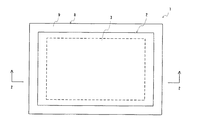
図1は、本実施形態に係る入力装置を示す概略平面図であり、図2は、図1の2−2における断面図である。 FIG. 1 is a schematic plan view showing an input device according to this embodiment, and FIG. 2 is a cross-sectional view taken along the line 2-2 in FIG.
図1および図2に示すように、本実施形態に係る入力装置1は、タッチパネル2を有し、タッチパネル2は、光透過性の材料からなる一対の検出基体3、4を有する。両検出基体3、4のうち入力側に配置される第1検出基体3は、薄膜材の一例としてのポリエステル等の材料からなる膜厚の薄い可撓性を有するフィルムからなる第1基体7aを有し、一方、反入力側に配置される第2検出基体4は、ガラスやアクリル等の材料からなる基板からなる第2基体7bを有しており、第1基体7aは、第2基体7bと比較して平面形状が大きく形成されている。
As shown in FIGS. 1 and 2, the
両基体7a、7bの相互に対向する内面には、それぞれ酸化インジウム錫等の光透過性の材料からなる第1検知手段および第2検知手段としての抵抗膜6a、6bが形成されており、各抵抗膜6a、6bには、それぞれ座標検出用の電圧が印加されるようになっている。また、第2検出基体4に形成された抵抗膜6bにおける入力側の面には、第1検出基体3と第2検出基体4との間隙を所定の寸法に保持するための図示しないスペーサが設けられている。
抵抗膜6a、6bがそれぞれ形成された両検出基体3、4は、平面形状において第1検出基体3の外周縁部分が第2検出基体4の外周縁から突出する位置において、所定の間隙をもって対向して配置され、第2検出基体4の内面4aにおける外周縁に配置された接着層5を介して一体に形成されている。
The two
そして、このタッチパネル2は、図示しない筆記具や指等の入力手段によって第1検出基体3の任意の位置が押圧操作されると、第1検出基体3が撓んで第1検出基体3の抵抗膜6aが、第2検出基体4の抵抗膜6bと接触し、この接触点における両抵抗膜6a、6bの間の抵抗比によって、この接触点の座標情報を検出し、この座標情報に基づいてデータが入力されるようになっている。
Then, when an arbitrary position of the
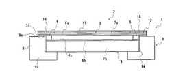
また、入力装置1は、タッチパネル2を収納する樹脂材料等からなる筐体8を有し、筐体8は、タッチパネル2の側面すなわち接着層5および第2検出基体4の側面の全体に対向して配置される側部9と、タッチパネル2の底面すなわち第2検出基体4の反入力側の面における外周縁部分に対向して配置されてタッチパネル2を支持する支持部10とを有し、側部9および支持部10は一体に形成されている。
The
そして、タッチパネル2は、第1検出基体3によって筐体8の側部9とタッチパネル2の側面との間隙14を筐体8の入力側から被覆するように、第1検出基体3の内面3aにおける外周縁を、側部9における入力側の頂面9aのうちタッチパネル2が収納される内部側の内側端縁に対向させることによって、筐体8の内部に収納されるようになっている。また、第1検出基体3の内面3aにおける外周縁は、側部9の頂面9aにおける内側端縁に、貼着材12を用いて貼着されている。
The
次に、本実施形態の作用について説明する。 Next, the operation of this embodiment will be described.
本実施形態によれば、第1検出基体3の第1基体7aは第2検出基体4の第2基体7bと比較して平面形状において大きく形成されている。そして、タッチパネル2は、第1検出基体3によって筐体8の側部9とタッチパネル2の側面との間隙14を筐体8の入力側から被覆するように、第1検出基体3の内面3aにおける周縁部分を、側部9における入力側の頂面9aのうちタッチパネル2が収納される内部側の内側端縁に対向させることによって、筐体8の内部に収納されている。このように、第1検出基体3によって筐体8の側部9とタッチパネル2の側面との間隙14が筐体8の入力側から被覆されているので、タッチパネル2の頂面9aの外周縁部分を被覆する頂壁を筐体8に備えることなく、タッチパネル2と筐体8との間隙14にごみや水分等の異物が侵入してしまうのを確実に防止することができる。
According to the present embodiment, the first base 7 a of the
したがって、第1検出基体3はフィルムにより構成されており、従来の筐体21における頂壁22よりも厚さ寸法が小さいので、入力装置1の薄型化を図ることができるとともに、タッチパネル2と筐体8との間隙14に異物が侵入するのを防止して、タッチパネル2の誤動作の発生するのを防止することができる。
Therefore, since the
また、第1検出基体3の内面3aは、側部9の頂面9aに貼着されているので、タッチパネル2を筐体8に固定し、タッチパネル2が筐体8から落下してしまうのを確実に防止することができるとともに、タッチパネル2と筐体8との間に異物が侵入するのをより確実に防止することができる。
In addition, since the
次に、本発明に係る入力装置1の第2の実施形態について図3および図4を参照して説明する。
Next, a second embodiment of the
ここで、第2の実施形態に係る入力装置について、第1の実施形態と同一の構成については、同一の符号を用いて説明し、詳説を省略する。 Here, regarding the input device according to the second embodiment, the same configuration as in the first embodiment will be described using the same reference numerals, and detailed description thereof will be omitted.
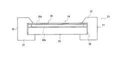
図3は、第2の実施形態における入力装置1を示す概略平面図、図4は図3の入力装置1の4−4における断面図である。
FIG. 3 is a schematic plan view showing the
図3および図4に示すように、タッチパネル2における第1検出基体3の反入力側の面の外周には、文字や図形等の装飾を印刷して形成される装飾層16が設けられている。本実施形態においては、タッチパネル2における第1検出基体3の反入力側の面のうち、タッチパネル2におけるデータの入力が可能な入力領域を除く非入力領域、すなわち、両検出基体3、4の内面における抵抗膜6a、6bが形成されていない位置や、両検出基体3、4を一体に形成する接着層5の配置位置およびその近傍には、本実施形態においてはタッチパネル2の外周縁部分に相当する位置に、装飾層16が形成されている。
As shown in FIGS. 3 and 4, a
そして、タッチパネル2は、第1検出基体3の外縁部分の内面3aが装飾層16を介して筐体8の側部9における頂面9aに対向するように、筐体8の内部に収納されており、第1検出基体3の内面3aは、装飾層16を介して筐体8の側部9における頂面9aに貼着材12を用いて貼着されている。
The
次に、第2の実施形態の作用について説明する。 Next, the operation of the second embodiment will be described.
本実施形態によれば、タッチパネル2の非入力領域に装飾層16が設けられており、これにより、入力装置1の入力側から、タッチパネル2における入力領域と非入力領域とを視認によって容易に判別することが可能となる。
According to the present embodiment, the
したがって、筆記用具等により非入力領域を押圧操作してしまうという誤動作を防止することができ、入力装置1におけるタッチパネル2の操作性の向上を図ることができる。
Therefore, it is possible to prevent a malfunction that the non-input area is pressed with a writing tool or the like, and the operability of the
また、第1の実施形態と同様に、従来の筐体21における頂壁22を形成せずに、頂壁22よりも厚さ寸法が小さいタッチパネル2の第1検出基体3によってタッチパネル2と筐体8との間隙14を被覆しながらタッチパネル2を筐体8に収納するので、入力装置1の薄型化を図ることができるとともに、タッチパネル2と筐体8との間隙14への異物の侵入を防止し、タッチパネル2の誤動作の発生を防止することができる。
Similarly to the first embodiment, the
さらに、装飾層16によって第2検出基体4の側面と筐体8の側部9との間隙を被覆することができ、これにより、入力装置1の入力側から、第2検出基体4の側面と筐体8の側部9との間隙が視認されてしまうのを防止することができる。
Furthermore, the
なお、第2の実施形態においては、装飾層16が第1検出基体3の反入力側の面に設けられているが、これに限定されるものではない。
In the second embodiment, the
図5は、装飾層16を備えたタッチパネル2を有する入力装置1のさらに他の実施形態を示す概略断面図である。図5に示すように、この入力装置1におけるタッチパネル2においては、第1検出基体3の入力側の面に装飾層16が設けられている。このタッチパネル2は、タッチパネル2における非入力領域に相当する位置に文字や模様等の装飾が印刷された装飾層16を有する装飾用フィルム17を有し、この装飾用フィルム17は、第1検出基体3の入力側に、装飾層16が第1検出基体3に対向するように配置されている。このタッチパネル2においても、タッチパネル2における入力領域と非入力領域とを視認により容易に判別することができ、これにより、筆記用具等による誤動作を防止して、入力装置1におけるタッチパネル2の操作性の向上を図ることができる。また、装飾用フィルム17により、装飾層を露出することなく保護することができる。
FIG. 5 is a schematic cross-sectional view showing still another embodiment of the
次に、本発明に係る入力装置の第3の実施形態について、図6および図7を用いて説明する。 Next, a third embodiment of the input device according to the present invention will be described with reference to FIGS.
図6は、第3の実施形態に係る入力装置の要部を示す概略断面図である。ここで、第3の実施形態に係る入力装置について、第1の実施形態に係る入力装置1と同一の構成については、同一の符号を用いて説明し、詳説を省略する。
FIG. 6 is a schematic cross-sectional view showing the main part of the input device according to the third embodiment. Here, regarding the input device according to the third embodiment, the same components as those of the
図6に示すように、筐体8における頂面9aのうち抵抗膜6aが形成された第1検出基体3の内面3aにおける外周縁部分に対向する位置には、凹部18が形成されている。この凹部18には、両面テープ等の貼着材12が配置されており、この貼着材12を介して、第1検出基体3の内面3aは、筐体8の頂面9aに貼着されている。
As shown in FIG. 6, a
筐体8の側部9は、第1検出基体3の内面3aに当接するとともに、第1検出基体3の第1抵抗膜6aと、第2検出基体4の第2抵抗膜6bとの間隙を所定の寸法に保持するようになっている。本実施形態においては、側部9には、第1検出基体3の内面3aと、第2検出基体4の内面4aとの間隙に配置されるように、タッチパネル2の配置側に突出する突出部19が形成されており、この突出部19により、両内面3a、4aの間隙、すなわち第1抵抗膜6aと第2抵抗膜6bとの間隙を所定の寸法に保持するようになっている。なお、側部9が第1抵抗膜6aと第2抵抗膜6bとの間隙を所定の寸法に保持する構成としては、本実施形態の形状に限定されるものではない。例えば、側部9に第2検出基体4の反入力側の面を支持する支持部を形成し、側部9の頂面9aによって第1検出基体3の内面3aを支持するとともに、支持部によって第2検出基体4の反入力側の面を支持することにより、側部9が第1抵抗膜6aと第2抵抗膜6bとの間隙を所定の寸法に保持するようにしてもよい。
The
側部9における突出部19の頂面9aには、第1検出基体3の内面3aとの当接部分を基端として、筐体8におけるタッチパネル2が配置される内部の方向に傾斜する傾斜面20が形成されている。本実施形態においては、傾斜面20は、第2抵抗膜6bにおける入力側の頂面の高さ位置まで傾斜する様に形成されている。
The
また、突出部19は、突出部19における反入力側の面が第2検出基体4の内面4a(本実施形態においては第2抵抗膜6bの内面)に対向するように、筐体8の側部9からタッチパネル2の配置側に突出するように形成されており、突出部19における反入力側の面は、第2検出基体4の内面4aに貼着材15を用いて貼着されている。
Further, the
第2抵抗膜6bにおける突出部19との対向部分を除く部分は、第2抵抗膜6bにおける他の部分と比較して高さ寸法が高く形成された上段部13とされており、突出部19における傾斜面20の終端部の高さ位置は、上段部13の入力側の頂面の高さ位置に形成されている。
A portion of the
また、この傾斜面20の傾斜角度(θ)は、第1検出基体3が入力領域の最外縁の近傍、すなわち突出部19の近傍において入力側から押圧された場合に、傾斜面20に沿って折曲された第1検出基体3の内面3aの第1抵抗膜6aの表面抵抗値が、折曲されていない場合と比較してほぼ変化しない程度に設定される。この傾斜角度(θ)は、隣辺(傾斜面の基端部と終端部とに相当する部分の間隙寸法)をLとし、対辺(第1抵抗膜6aと第2抵抗膜6bとの間隙寸法)をhとするとき、θ=tan−1h/L≦2.9°であることが好ましい。
The inclination angle (θ) of the
このような入力装置1のタッチパネル2においては、第1および第2の各実施形態に係る入力装置1のタッチパネル2と異なり、第1検出基体3と第2検出基体4との間隙に接着層5が配置されていない。
Unlike the
次に、本実施形態の作用について説明する。 Next, the operation of this embodiment will be described.
本実施形態によれば、突出部19は、第1検出基体3の内面3aとの当接部を基端として、第2抵抗膜6bにおける入力側の頂面の高さ位置まで傾斜する傾斜面20を有している。このため、突出部19の近傍において第1検出基体3を押圧した場合であっても、第1検出基体3は、傾斜面20に沿って折曲されるので、第1検出基体3が過度に折曲されてしまうのを防止することができる。
According to the present embodiment, the projecting
したがって、本実施形態によれば、第1検出基体3が入力領域の最外縁の近傍において入力側から押圧された場合であっても、第1検出基体3を突出部19の傾斜面20に沿って折曲させて、第1検出基体3が過度に折曲されてしまうのを防止することにより、第1検出基体3における折曲された部分に形成された第1抵抗膜6aに亀裂等が発生してしまうのを防止することができる。
Therefore, according to this embodiment, even when the
また、この傾斜面20の傾斜角度(θ)を、第1検出基体3が傾斜面20に沿って折曲された場合に対応する第1抵抗膜6aの表面抵抗値がほぼ変化しない程度に設定し、さらにはθ=tan−1h/L≦2.9°に設定することにより、第1検出基体3が過度に折曲されて、第1抵抗膜6aに亀裂等が発生してしまうのをより確実に防止することができる。
Further, the inclination angle (θ) of the
さらに、第2抵抗膜6bに上段部13を形成することにより、上段部が形成されている部分の第2抵抗膜6bと第1抵抗膜6aとの間隙寸法を調整することができる。このため、上段部13の高さ寸法を調整することにより、傾斜面20の傾斜角度(tan−1θ)を所定の角度となるように設定することができる。
Furthermore, by forming the
さらにまた、突出部19を貼着材15を介して第2検出基体4の内面4aに貼着することにより、タッチパネル2を筐体8に固定することができるとともに、タッチパネル2と筐体8との間に異物が侵入するのをより確実に防止することができる。
Furthermore, by sticking the
また、筐体8の側部9における頂面9aに、筐体8と第1検出基体3の内面3aとを貼着するための貼着材12を配置する凹部18が形成されており、これにより、筐体8の頂面とタッチパネル2の入力側の面とをより面一にすることができる。
Further, a
さらに、図6には図示しないが、図4および図5と同様にして、第1検出基体3のデータ入力が可能な入力領域を除く非入力領域(本実施形態においては、第2検出基体4の上段部13の外縁より外側部分)を覆う装飾層を設けてもよい。 Further, although not shown in FIG. 6, in the same manner as in FIGS. 4 and 5, a non-input area (in the present embodiment, the second detection base 4) excluding the input area where data can be input. You may provide the decoration layer which covers a part outside the outer edge of the upper stage part 13).
なお、本発明は前記各実施形態に限定されるものではなく、必要に応じて種々変更することが可能である。 The present invention is not limited to the above-described embodiments, and various modifications can be made as necessary.
例えば、前記各実施形態においては、筐体8の側部9はタッチパネル2からなる入力パネルの側面全体に対向して形成されているとともに、筐体8の支持部10は入力パネルの底面の外周縁に対向して形成されているが、これに限定されるものではなく、少なくとも入力パネルの側面および底面の一部に対向する側部9および支持部10を有し、入力パネルを収納・保持することができればよい。
For example, in each of the above embodiments, the
1 入力装置
2 タッチパネル
3 第1検出基体
3a 内面
4 第2検出基体
5 接着層
6 抵抗膜
7a 第1基体
7b 第2基体
8 筐体
9 側部
9a 頂面
10 支持部
12 貼着材
14 間隙
DESCRIPTION OF
Claims (14)
前記両検出基体のうち入力側に位置する第1検出基体は、薄膜材により構成された第1基体を有し、前記第1基体は、反入力側に位置する第2検出基体に設けられた第2基体と比較して平面形状が大きく形成されており、
前記筐体は、前記入力パネルのうち前記第2検出基体の側面に対向して配置される側部と、前記第2検出基体の反入力側の底面に対向して配置される支持部とを有し、
前記第2検出基体は、前記筐体の前記側部から前記支持部にかけての空間内に収納され、前記第2基体よりも延出した前記第1基体の外周縁は、その反入力側の面である内面が前記筐体の前記側部における入力側の頂面に対向されており、前記第1検出基体によって前記筐体の前記側部と前記第2検出基体の側面との間隙が前記筐体の入力側から被覆されることを特徴とする入力装置。 A pair of detection bases are arranged to face each other in the height direction, and is an input device having an input panel capable of inputting data by an operation by an input means and a housing ,
The first detection base located on the input side of the both detection bases has a first base made of a thin film material, and the first base is provided on the second detection base located on the opposite input side. The planar shape is formed larger than the second substrate,
The housing includes a side portion of the input panel that is disposed to face the side surface of the second detection base, and a support portion that is disposed to face the bottom surface of the second detection base opposite to the input side. Have
The second detection base is housed in a space from the side portion to the support portion of the housing, and an outer peripheral edge of the first base extending from the second base is a surface on the opposite side to the second detection base. in it the inner surface are opposed to the top surface of the input side of the side of the housing, the gap between the side face of the side and the second detection base of the housing by the first detection base is the An input device that is covered from an input side of a housing .
前記第2検知手段における高さ方向への前記突出部との対向部分を除く部分は、第2検出手段における他の部分と比較して高さ寸法を高く形成された上段部とされており、
前記傾斜面の終端部の高さ位置は、前記上段部の頂面の高さ位置とすることを特徴とする請求項4または請求項5に記載の入力装置。 The side portion projects toward the arrangement side of the input panel so as to be arranged in a gap between the inner surface of the first detection base and the inner surface of the second detection base on which the second detection means is formed. Having protrusions formed,
The portion of the second detection means excluding the portion facing the protrusion in the height direction is an upper stage formed with a height dimension higher than that of the other parts of the second detection means,
The input device according to claim 4, wherein a height position of a terminal portion of the inclined surface is a height position of a top surface of the upper stage portion.
前記第1基体は、前記第2基体よりも大きく形成されて、前記第1基体には、前記第2基体から外方にはみ出して、筐体との接合領域である外周縁が設けられていることを特徴とする入力パネル。 A first base located on the input side, a second base located on the non-input side, a decorative layer provided on the outer periphery of the first base on the non-input side, and provided on the non-input side of the decorative layer First detection means, and second detection means provided on the input side of the second base,
Wherein the first substrate, the second is larger than the substrate, wherein the first substrate, the protruding and outwardly from the second substrate, and the outer peripheral edge is a junction region between the housing provided An input panel characterized by that.
前記第2基体及び前記第2検知手段は、前記筐体に設けられた収納部に収納され、前記第1基体の外周縁における反入力側の面が、前記筐体の前記収納部を画定する側部の入力側の頂部と対向していることを特徴とする入力装置。 An input device having an input panel according to claim 12 and a housing,
The second base and the second detection means are housed in a housing provided in the housing, and a surface on the non-input side of the outer periphery of the first base defines the housing of the housing. An input device, wherein the input device faces the input side top of the side portion.
Priority Applications (4)
| Application Number | Priority Date | Filing Date | Title |
|---|---|---|---|
| JP2006187989A JP4740055B2 (en) | 2006-07-07 | 2006-07-07 | Input device and input panel |
| US11/773,315 US8044938B2 (en) | 2006-07-07 | 2007-07-03 | Input device with improved touch panel surface and electronic device having the input device |
| CNB2007101283154A CN100547533C (en) | 2006-07-07 | 2007-07-06 | Input media |
| CN2009101269512A CN101504581B (en) | 2006-07-07 | 2007-07-06 | Input device |
Applications Claiming Priority (1)
| Application Number | Priority Date | Filing Date | Title |
|---|---|---|---|
| JP2006187989A JP4740055B2 (en) | 2006-07-07 | 2006-07-07 | Input device and input panel |
Publications (3)
| Publication Number | Publication Date |
|---|---|
| JP2008015885A JP2008015885A (en) | 2008-01-24 |
| JP2008015885A5 JP2008015885A5 (en) | 2010-08-19 |
| JP4740055B2 true JP4740055B2 (en) | 2011-08-03 |
Family
ID=39035828
Family Applications (1)
| Application Number | Title | Priority Date | Filing Date |
|---|---|---|---|
| JP2006187989A Expired - Fee Related JP4740055B2 (en) | 2006-07-07 | 2006-07-07 | Input device and input panel |
Country Status (3)
| Country | Link |
|---|---|
| US (1) | US8044938B2 (en) |
| JP (1) | JP4740055B2 (en) |
| CN (2) | CN100547533C (en) |
Families Citing this family (9)
| Publication number | Priority date | Publication date | Assignee | Title |
|---|---|---|---|---|
| JP2009032417A (en) * | 2007-07-24 | 2009-02-12 | Nissha Printing Co Ltd | Protection panel with touch input function and its manufacturing method |
| TWI374379B (en) | 2007-12-24 | 2012-10-11 | Wintek Corp | Transparent capacitive touch panel and manufacturing method thereof |
| KR101064184B1 (en) * | 2009-07-01 | 2011-09-14 | 권성철 | Touch panels and preparation methods thereof |
| JP5533364B2 (en) * | 2010-07-06 | 2014-06-25 | パナソニック株式会社 | Touch panel |
| US8564559B2 (en) * | 2010-12-22 | 2013-10-22 | Universal Cement Corporation | Cover glass button for display of mobile device |
| JP5800551B2 (en) * | 2011-04-04 | 2015-10-28 | 富士通コンポーネント株式会社 | Resistive touch panel |
| CN103562825B (en) | 2011-05-30 | 2016-08-17 | Nlt科技股份有限公司 | Display device |
| JP5753501B2 (en) * | 2012-02-10 | 2015-07-22 | ホシデン株式会社 | Component module |
| US9501186B2 (en) * | 2013-07-12 | 2016-11-22 | Xiaomi Inc. | Touch screen and mobile terminal including same |
Family Cites Families (14)
| Publication number | Priority date | Publication date | Assignee | Title |
|---|---|---|---|---|
| JPH0683537A (en) | 1992-09-01 | 1994-03-25 | Ricoh Co Ltd | Touch panel type information processor |
| JPH08241646A (en) * | 1995-03-03 | 1996-09-17 | Nissha Printing Co Ltd | Transparent touch panel |
| US6357887B1 (en) * | 1999-05-14 | 2002-03-19 | Apple Computers, Inc. | Housing for a computing device |
| JP2002023928A (en) * | 2000-07-03 | 2002-01-25 | Japan Aviation Electronics Industry Ltd | Input device for numeral and character |
| KR100617028B1 (en) * | 2000-12-28 | 2006-08-30 | 엘지.필립스 엘시디 주식회사 | Liquid Crystal Display Device installed EGIP |
| JP4066641B2 (en) * | 2001-11-20 | 2008-03-26 | 松下電器産業株式会社 | Touch panel |
| JP2004213187A (en) * | 2002-12-27 | 2004-07-29 | Nissha Printing Co Ltd | Touch panel with icon |
| KR100628265B1 (en) * | 2003-11-24 | 2006-09-27 | 엘지.필립스 엘시디 주식회사 | Touch Panel in Resistive Type |
| CN100405269C (en) | 2003-12-26 | 2008-07-23 | 日本写真印刷株式会社 | Electronic apparatus with protection panel, protection panel, and method of producing protection panel |
| JP4341424B2 (en) * | 2004-02-06 | 2009-10-07 | ソニー株式会社 | Display device |
| JP2005242501A (en) | 2004-02-25 | 2005-09-08 | Nec Corp | Panel structure and its mounting structure |
| US7342573B2 (en) * | 2004-07-07 | 2008-03-11 | Nokia Corporation | Electrostrictive polymer as a combined haptic-seal actuator |
| JP2006106912A (en) * | 2004-10-01 | 2006-04-20 | Citizen Watch Co Ltd | Information input device and method for manufacturing the same |
| KR20150038558A (en) * | 2006-11-30 | 2015-04-08 | 탭이뮨, 인크. | Poxviridae treatment comprising TAP-1 and/or TAP-2 as a molecular adjuvant |
-
2006
- 2006-07-07 JP JP2006187989A patent/JP4740055B2/en not_active Expired - Fee Related
-
2007
- 2007-07-03 US US11/773,315 patent/US8044938B2/en not_active Expired - Fee Related
- 2007-07-06 CN CNB2007101283154A patent/CN100547533C/en not_active Expired - Fee Related
- 2007-07-06 CN CN2009101269512A patent/CN101504581B/en not_active Expired - Fee Related
Also Published As
| Publication number | Publication date |
|---|---|
| US8044938B2 (en) | 2011-10-25 |
| JP2008015885A (en) | 2008-01-24 |
| CN101504581B (en) | 2011-12-21 |
| US20080122793A1 (en) | 2008-05-29 |
| CN100547533C (en) | 2009-10-07 |
| CN101504581A (en) | 2009-08-12 |
| CN101101528A (en) | 2008-01-09 |
Similar Documents
| Publication | Publication Date | Title |
|---|---|---|
| JP4740055B2 (en) | Input device and input panel | |
| JP7411007B2 (en) | Devices with integrated interface system | |
| US20180159969A1 (en) | Electronic Devices with Concave Displays | |
| KR100894277B1 (en) | Mobile terminal | |
| JP5325646B2 (en) | Touch screen panel | |
| US8259079B2 (en) | Input panel having flexible circuit board inserted into passage through base and input device having the input panel | |
| US10514798B2 (en) | Touch panel with fingerprint identification function and method for fabricating the same | |
| US10353485B1 (en) | Multifunction input device with an embedded capacitive sensing layer | |
| JP2016143420A (en) | Touch device | |
| KR20130102131A (en) | Touch screen stack-ups | |
| JP5909560B2 (en) | Input device, display device, and electronic device | |
| US20110181445A1 (en) | Key sheet | |
| JP2009038796A (en) | Handheld electronic apparatus, and touch panel thereof | |
| JP5933035B2 (en) | Input device, display device, and electronic device | |
| JP2008021304A (en) | Input device | |
| US20100182254A1 (en) | Touch screen panel | |
| US9046972B2 (en) | Structure for a tactile display | |
| JP5300961B2 (en) | Input device, display device, and portable terminal | |
| WO2013111508A1 (en) | Input device, display device, and electronic equipment | |
| JPWO2018168387A1 (en) | Touch panel and design structure having the same | |
| JP2008071239A (en) | Input device | |
| JP2013061854A (en) | Keyboard device, and information processor using the keyboard device | |
| KR20210101428A (en) | Electronic device including display | |
| JP6244898B2 (en) | Touch-type information input image display device and information device | |
| JP2012248010A (en) | Input device, display apparatus, and equipment |
Legal Events
| Date | Code | Title | Description |
|---|---|---|---|
| A621 | Written request for application examination |
Free format text: JAPANESE INTERMEDIATE CODE: A621 Effective date: 20080905 |
|
| RD02 | Notification of acceptance of power of attorney |
Free format text: JAPANESE INTERMEDIATE CODE: A7422 Effective date: 20100604 |
|
| RD04 | Notification of resignation of power of attorney |
Free format text: JAPANESE INTERMEDIATE CODE: A7424 Effective date: 20100602 |
|
| A521 | Written amendment |
Free format text: JAPANESE INTERMEDIATE CODE: A523 Effective date: 20100706 |
|
| A977 | Report on retrieval |
Free format text: JAPANESE INTERMEDIATE CODE: A971007 Effective date: 20100813 |
|
| A131 | Notification of reasons for refusal |
Free format text: JAPANESE INTERMEDIATE CODE: A131 Effective date: 20101012 |
|
| A521 | Written amendment |
Free format text: JAPANESE INTERMEDIATE CODE: A523 Effective date: 20101207 |
|
| A01 | Written decision to grant a patent or to grant a registration (utility model) |
Free format text: JAPANESE INTERMEDIATE CODE: A01 Effective date: 20110419 |
|
| A01 | Written decision to grant a patent or to grant a registration (utility model) |
Free format text: JAPANESE INTERMEDIATE CODE: A01 |
|
| A61 | First payment of annual fees (during grant procedure) |
Free format text: JAPANESE INTERMEDIATE CODE: A61 Effective date: 20110428 |
|
| R150 | Certificate of patent or registration of utility model |
Free format text: JAPANESE INTERMEDIATE CODE: R150 |
|
| FPAY | Renewal fee payment (event date is renewal date of database) |
Free format text: PAYMENT UNTIL: 20140513 Year of fee payment: 3 |
|
| LAPS | Cancellation because of no payment of annual fees |