JP2006106912A - Information input device and method for manufacturing the same - Google Patents

Information input device and method for manufacturing the same Download PDF

Info

Publication number
JP2006106912A
JP2006106912A JP2004289455A JP2004289455A JP2006106912A JP 2006106912 A JP2006106912 A JP 2006106912A JP 2004289455 A JP2004289455 A JP 2004289455A JP 2004289455 A JP2004289455 A JP 2004289455A JP 2006106912 A JP2006106912 A JP 2006106912A
Authority
JP
Japan
Prior art keywords
insulating film
electrode
substrate
icon display
touch panel
Prior art date
Legal status (The legal status is an assumption and is not a legal conclusion. Google has not performed a legal analysis and makes no representation as to the accuracy of the status listed.)
Pending
Application number
JP2004289455A
Other languages
Japanese (ja)
Inventor
Yoshikazu Matsumura
松村  佳和
Current Assignee (The listed assignees may be inaccurate. Google has not performed a legal analysis and makes no representation or warranty as to the accuracy of the list.)
Citizen Watch Co Ltd
Original Assignee
Citizen Watch Co Ltd
Priority date (The priority date is an assumption and is not a legal conclusion. Google has not performed a legal analysis and makes no representation as to the accuracy of the date listed.)
Filing date
Publication date
Application filed by Citizen Watch Co Ltd filed Critical Citizen Watch Co Ltd
Priority to JP2004289455A priority Critical patent/JP2006106912A/en
Publication of JP2006106912A publication Critical patent/JP2006106912A/en
Pending legal-status Critical Current

Links

Images

Abstract

<P>PROBLEM TO BE SOLVED: To provide an information input device and a picture input type display device which are easily assembled at low costs. <P>SOLUTION: An insulating film 45 for icon display for a fixed key having notched sections 45a, 45b, 45c, 45d and 45e is installed on the touch electrode of at least one substrate of upper and lower substrates 11 and 41 of a touch panel 40 formed by bonding the upper and the lower substrates 11 and 41 with a fixed interval. The notched sections are shaped so that the types of icons are recognized from characters or symbols, graphics or patterns or the like, and formed so that the switch operations of the ions are performed in the notched sections. Also, the notched sections are installed in an active area. Also, an insulating film for icon display is colored so as to be made opaque so that the icons are identified. <P>COPYRIGHT: (C)2006,JPO&NCIPI

Description

本発明は情報入力装置に関し、特に、ATM、カーナビゲーション、自動販売機、複写機、各種端末機等の機器や電子手帳、ワードプロセッサー、パーソナルコンピュータなどに用いられて、液晶ディスプレイ等の表示画面上に配置し、透視した画面の指示に従って使用者が情報の表示画面を指やペンで直接押してデータの入力を行ったり、手書きの文字入力を行ったりする情報入力装置に関する。   The present invention relates to an information input device, and in particular, used in devices such as ATMs, car navigation systems, vending machines, copying machines, various terminals, electronic notebooks, word processors, personal computers, etc., on a display screen such as a liquid crystal display. The present invention relates to an information input apparatus in which a user inputs data by directly pressing a display screen of information with a finger or a pen according to an instruction on a screen that is arranged and seen through, or inputs handwritten characters.

情報入力装置の代表的な一つに抵抗膜式タッチパネルがある。背景技術を説明するに当たりこの抵抗膜式タッチパネルを用いて説明する。従来技術における抵抗膜式タッチパネルは、可撓性を有する透明基板の下面にタッチ電極とこのタッチ電極に接続する配線電極を形成した上基板と、同じく、透明基板の上面にタッチ電極とこのタッチ電極に接続する配線電極を形成し、タッチ電極の上面にドットスペーサを一定間隔に配設した下基板とが、所定の隙間を持ってタッチ電極同士が対面するような配置構造を取っている。そして、このタッチパネルを液晶表示装置等の表示装置の上面側に配置して使用される。表示装置の表示部分に位置する所のタッチパネルを指又はペンで押すことによって、タッチパネルの上基板が撓んでその押した所のタッチ電極が下基板のタッチ電極に接触し、そして、その接触点の位置が電気抵抗の測定によって検知されて入力情報が読みとられる。   One typical information input device is a resistive touch panel. The background art will be described using this resistive touch panel. The resistive film type touch panel in the prior art has an upper substrate in which a touch electrode and a wiring electrode connected to the touch electrode are formed on the lower surface of a flexible transparent substrate, and the touch electrode and the touch electrode on the upper surface of the transparent substrate. A wiring electrode to be connected to the lower electrode, and a lower substrate having dot spacers arranged at regular intervals on the upper surface of the touch electrode, is arranged so that the touch electrodes face each other with a predetermined gap. The touch panel is used by being arranged on the upper surface side of a display device such as a liquid crystal display device. By pressing the touch panel located at the display portion of the display device with a finger or a pen, the upper substrate of the touch panel is bent and the touch electrode at the pressed position comes into contact with the touch electrode on the lower substrate. The position is detected by measuring electrical resistance and the input information is read.

ここで、一般的に用いられている従来技術の抵抗膜式タッチパネル(以降、単にタッチパネルと云う)の構成を図12〜15を用いて説明する。尚、図12は従来技術におけるタッチパネルの平面図、図13は図12おけるC−C断面図、図14は図12における下基板の平面図、図15は図12における上基板の平面図を示している。   Here, a configuration of a commonly used resistive film type touch panel (hereinafter simply referred to as a touch panel) will be described with reference to FIGS. 12 is a plan view of a conventional touch panel, FIG. 13 is a cross-sectional view taken along the line CC in FIG. 12, FIG. 14 is a plan view of the lower substrate in FIG. 12, and FIG. 15 is a plan view of the upper substrate in FIG. ing.

図12、図13、図14、図15に示すように、従来技術のタッチパネル20は形状が方形をなす下基板1と可撓性を有する上基板11とが主要構成部品となって構成されている。下基板1は、図14に示すように、透明な方形のガラスからなる透明基板2と、この透明基板2の上面に方形形状に形成された下タッチ電極3と、この下タッチ電極3の図14の中で上下の対向した両辺に沿って接続形成されて透明基板2の下方延設部にあるFPC取付部S(図14の中で、下側の点線枠の部分)にまで引き回した一対の配線電極4及び5と、FPC取付部S近辺に形成された一対の接続電極8、9と、下タッチ電極3上にマトリックス状に配置したドットスペーサ10と、一対の配線電極4、5の面上に設けられた絶縁膜6、7とで構成されている。尚、配線電極4は、図14の中で下タッチ電極3の下辺に接続した部分の電極4aと、そこからFPC取付部Sに向かって引き回した部分の電極4bとで構成されている。また、配線電極5は、図14の中で下タッチ電極3の上辺に接続した部分の電極5aと、透明基板2の右端側の外周域に沿って引き回した部分の電極5bと、FPC取付部Sに向かった部分の電極5c、5dとで構成されている。そして、絶縁膜6は配線電極4aの部分に設けられ、絶縁膜7は配線電極5a、5b、5cの部分に設けられている。この絶縁膜は後述する上基板のタッチ電極や一対の配線電極と近接する部分に設けられ、接触導通の防止を図っている。また、絶縁膜は損傷からの保護膜の働きも兼ねている。また、一対の接続電極8、9は、後述する上基板11の配線電極14、15に導通接続を行うためにFPC取付部S近辺に設けており、図12に示すように、上基板11の配線電極14、15と接続部B、Aの箇所において接続される。   As shown in FIG. 12, FIG. 13, FIG. 14, and FIG. 15, the touch panel 20 of the prior art is composed of a lower substrate 1 having a square shape and an upper substrate 11 having flexibility as main components. Yes. As shown in FIG. 14, the lower substrate 1 includes a transparent substrate 2 made of transparent square glass, a lower touch electrode 3 formed in a square shape on the upper surface of the transparent substrate 2, and a diagram of the lower touch electrode 3. 14, a pair formed to be connected along both upper and lower opposing sides and routed to an FPC mounting portion S (a portion of a lower dotted line frame in FIG. 14) in a downwardly extending portion of the transparent substrate 2. Wiring electrodes 4 and 5, a pair of connection electrodes 8 and 9 formed in the vicinity of the FPC attachment portion S, dot spacers 10 arranged in a matrix on the lower touch electrode 3, and a pair of wiring electrodes 4 and 5. It is comprised with the insulating films 6 and 7 provided on the surface. The wiring electrode 4 is composed of a portion of the electrode 4a connected to the lower side of the lower touch electrode 3 in FIG. 14 and a portion of the electrode 4b routed from there to the FPC mounting portion S. The wiring electrode 5 includes a portion of the electrode 5a connected to the upper side of the lower touch electrode 3 in FIG. 14, a portion of the electrode 5b routed along the outer peripheral area on the right end side of the transparent substrate 2, and an FPC attachment portion. It consists of electrodes 5c and 5d in the portion facing S. The insulating film 6 is provided on the wiring electrode 4a, and the insulating film 7 is provided on the wiring electrodes 5a, 5b, and 5c. This insulating film is provided in a portion close to a touch electrode and a pair of wiring electrodes on the upper substrate, which will be described later, to prevent contact conduction. The insulating film also serves as a protective film against damage. Further, the pair of connection electrodes 8 and 9 are provided in the vicinity of the FPC mounting portion S in order to make conductive connection to wiring electrodes 14 and 15 of the upper substrate 11 to be described later, and as shown in FIG. The wiring electrodes 14 and 15 are connected to the connection portions B and A.

上基板11は、図15に示すように、可撓性のある透明な基材からなる透明基板12と、この透明基板12の下面に方形形状に形成されている上タッチ電極13と、この上タッチ電極13の図15の中で左右の対向する両辺に沿って接続形成されて下基板1のFPC
取付部S方向に向かって引き回した一対の配線電極14、15と、一対の配線電極14、15の面上に設けられた絶縁膜16、17とで構成されている。尚、配線電極14は、図15の中で上タッチ電極13の左辺に接続した部分の電極14aとFPC取付部Sに向かって引き回した電極14bとから構成され、同様に、配線電極15は、図15の中で上タッチ電極13の右辺に接続した部分の電極15aとFPC取付部Sに向かって引き回した電極15bとから構成されている。そして、絶縁膜16は配線電極14a、14bに設けられ、絶縁膜17は配線電極15a、15bに設けられるが、配線電極14bの先端部14b1、及び配線電極15bの先端部15b1は下基板1の接続電極8、9と接続する部分であるので絶縁膜は設けていない。この絶縁膜16、17は、下基板1の絶縁膜と同様に、接触導通防止目的、並びに保護目的で設けている。
As shown in FIG. 15, the upper substrate 11 includes a transparent substrate 12 made of a flexible transparent base material, an upper touch electrode 13 formed in a rectangular shape on the lower surface of the transparent substrate 12, The FPC of the lower substrate 1 is formed by connecting along both the left and right opposing sides of the touch electrode 13 in FIG.
A pair of wiring electrodes 14 and 15 routed in the direction of the mounting portion S and insulating films 16 and 17 provided on the surfaces of the pair of wiring electrodes 14 and 15 are configured. The wiring electrode 14 is composed of a portion of the electrode 14a connected to the left side of the upper touch electrode 13 in FIG. 15 and an electrode 14b routed toward the FPC mounting portion S. Similarly, the wiring electrode 15 includes: In FIG. 15, the electrode 15a is connected to the right side of the upper touch electrode 13 and the electrode 15b is routed toward the FPC attachment portion S. The insulating film 16 is provided on the wiring electrodes 14a and 14b, and the insulating film 17 is provided on the wiring electrodes 15a and 15b. The tip portion 14b1 of the wiring electrode 14b and the tip portion 15b1 of the wiring electrode 15b are formed on the lower substrate 1. Since it is a part connected to the connection electrodes 8 and 9, no insulating film is provided. The insulating films 16 and 17 are provided for the purpose of preventing contact conduction and protecting, like the insulating film of the lower substrate 1.

そして、図12、図13に示すように、上基板11の配線電極14(14a部分)、15(15a部分)と下基板1の配線電極4(4a部分)、及び5(5a部分)が方形の対向辺に配置されるように対向配置して、シール材18を介して下基板1と上基板11を一定の隙間を持たせて接合し、上基板11と下基板1の外周域を周回してシールしている。更に、上基板11に設けられた配線電極14及び15は、接続部B及びAの場所において、その先端部14b1、15b1が下基板1に設けた接続電極8及び9と導電性接着剤、あるいは異方性導電接着剤などを介して接続され、導通がとられている。   12 and 13, the wiring electrodes 14 (14a portion) and 15 (15a portion) of the upper substrate 11 and the wiring electrodes 4 (4a portion) and 5 (5a portion) of the lower substrate 1 are square. The lower substrate 1 and the upper substrate 11 are joined to each other so as to be disposed on the opposite sides of the substrate, with a certain gap, and the outer periphery of the upper substrate 11 and the lower substrate 1 is circulated. And sealed. Further, the wiring electrodes 14 and 15 provided on the upper substrate 11 are connected to the connection electrodes 8 and 9 provided on the lower substrate 1 at the locations of the connection portions B and A and the conductive electrodes, It is connected through an anisotropic conductive adhesive or the like to conduct electricity.

上記構成のタッチパネル20は、上基板11の一対の配線電極14、15、及び下基板1の一対の配線電極4、5の外側部分をシール材18で一周に渡ってシールした構造を取ってるものであるが、他の構造のものとしては、配線電極の形成部分をシール材で一周に渡ってシールして狭額縁化を図った構造のものもある。   The touch panel 20 configured as described above has a structure in which the outer portions of the pair of wiring electrodes 14 and 15 of the upper substrate 11 and the pair of wiring electrodes 4 and 5 of the lower substrate 1 are sealed with a sealing material 18 over the entire circumference. However, as another structure, there is a structure in which the portion where the wiring electrode is formed is sealed with a sealing material over the entire circumference to narrow the frame.

上記の構成を取るタッチパネル20の各構成要素部品は次のようになっている。下基板1を構成する透明基板2は透明なガラスが用いられる。このガラスはソーダガラスや石英ガラス、アルカリガラス、ホウケイ酸ガラス、普通板ガラス等が利用でき、反り等が起きない程度の厚さのものが使われる。多くは0.7〜1.1mmのものが選択される。上基板11を構成する透明基板12は可撓性を必要とするところなので透明な薄板ガラスや透明なプラスチックフイルムなどが用いられる。例えば、カーナビゲーション等のように耐熱性が求められる機器に用いられるものは、耐熱性や衝撃性にも強く、且つ可撓性も有する0.2mm厚みのマイクロシートガラスなどが多く用いられている。また、プラスチックフィルムとしては、0.1〜0.2mm厚みのPETフィルム(ポリエチレンテレフタレートフィルム)やポリカーボネイトフィルムなどが主に用いられている。   Each component part of the touch panel 20 having the above-described configuration is as follows. Transparent glass is used for the transparent substrate 2 constituting the lower substrate 1. As this glass, soda glass, quartz glass, alkali glass, borosilicate glass, normal plate glass, and the like can be used, and those having a thickness that does not cause warpage or the like are used. In many cases, 0.7 to 1.1 mm is selected. Since the transparent substrate 12 constituting the upper substrate 11 requires flexibility, a transparent thin glass or a transparent plastic film is used. For example, those used in devices that require heat resistance such as car navigation are often used as 0.2 mm-thick microsheet glass that is strong in heat resistance and impact resistance and has flexibility. . As the plastic film, a PET film (polyethylene terephthalate film) or a polycarbonate film having a thickness of 0.1 to 0.2 mm is mainly used.

下基板1を構成する下タッチ電極3及び上基板11を構成する上タッチ電極13は錫をドープした酸化インジウムのITO(Indium Tin Oxide)膜で形成した透明な薄膜からなっている。このITO膜は真空蒸着法、スパッタリング法、CVD法、印刷法等で形成する。この下タッチ電極3及び上タッチ電極13は高抵抗値であることが求められるために、250〜500オングストロームの範囲で非常に薄く形成する。そして、基板全面に形成したITO膜をフォトリソグラフィにより不要部分を除去し、必要な部分を残して形成する。   The lower touch electrode 3 constituting the lower substrate 1 and the upper touch electrode 13 constituting the upper substrate 11 are made of a transparent thin film formed of an indium oxide ITO (Indium Tin Oxide) film doped with tin. This ITO film is formed by a vacuum deposition method, a sputtering method, a CVD method, a printing method, or the like. Since the lower touch electrode 3 and the upper touch electrode 13 are required to have a high resistance value, they are formed very thin in the range of 250 to 500 angstroms. Then, the ITO film formed on the entire surface of the substrate is formed by removing unnecessary portions by photolithography and leaving necessary portions.

下基板1を構成する一対の配線電極4、5、一対の接続電極8、9、及び上基板11を構成する一対の配線電極14、15は、銀ペーストなどの高導電率のペーストを用いてスクリーン印刷等の印刷方法で形成する。タッチパネルの性能上、これらの電極の抵抗値が低ければ低いほど良いものであり、一般に、タッチ電極のシート抵抗値に対してこれらの電極のシート抵抗値は100分の1以下であることが必要とされている。そこで、これらの電極の印刷の厚さを増したり、幅を広くしたりして抵抗値を小さく押さえる設計がなされている。   The pair of wiring electrodes 4 and 5 constituting the lower substrate 1, the pair of connection electrodes 8 and 9, and the pair of wiring electrodes 14 and 15 constituting the upper substrate 11 are made of a high conductivity paste such as silver paste. It is formed by a printing method such as screen printing. In view of the performance of the touch panel, the lower the resistance value of these electrodes, the better. In general, the sheet resistance value of these electrodes needs to be 1/100 or less of the sheet resistance value of the touch electrode. It is said that. Therefore, a design has been made to reduce the resistance value by increasing the thickness of printing of these electrodes or increasing the width.

下基板1を構成するドットスペーサ10は、押圧した部分以外の部分の上下のタッチ電極同士が接触しないために設けるもので、透明なアクリル樹脂、エポキシ樹脂、ウレタン樹脂、その他の透明な樹脂材料をスクリーン印刷等の方法でドットマトリックス状に一定間隔に形成し、その後、熱または紫外線で硬化処理を施して形成する。このドットスペーサ10は目に見えない大きさであることが求められることから、直径は30〜60μm、ドット間隔は1〜8mmの範囲で設計される。高さは、透明基板12に薄板ガラスを用いた場合とプラスチックフィルムを用いた場合とで異なるが、薄板ガラスを用いた場合には2〜5μm、プラスチックフィルムを用いた場合には10μm前後の範囲で形成する。   The dot spacer 10 constituting the lower substrate 1 is provided so that the upper and lower touch electrodes other than the pressed portion do not come into contact with each other, and transparent acrylic resin, epoxy resin, urethane resin, and other transparent resin materials are used. It is formed in a dot matrix at regular intervals by a method such as screen printing, and then subjected to a curing treatment with heat or ultraviolet rays. Since the dot spacer 10 is required to be invisible, the diameter is designed in the range of 30 to 60 μm and the dot interval is 1 to 8 mm. The height differs depending on whether a thin glass is used for the transparent substrate 12 or a plastic film, but ranges from 2 to 5 μm when a thin glass is used, and around 10 μm when a plastic film is used. Form with.

シール材18は、上基板11と下基板1とを接合する目的、内部に水分などの進入を防止する目的で設けるが、同時に、上下基板11、1を所定の間隙量に設定する目的も兼ねている。このシール材18はスペーサボールを分散させたエポキシ樹脂接着剤やアクリル樹脂接着剤等をスクリーン印刷等の方法で印刷して形成する。厚みは、上透明基板12に薄板ガラスを用いた場合とプラスチックフィルムを用いた場合とで異なるが、薄板ガラスを用いた場合には上下基板11、1の接着後の間隙が10μm前後、プラスチックフィルムを用いた場合には上下基板11、1の接着後の間隙が略100〜200μmの範囲に設定している。スペーサボールは上基板11と下基板1との隙間を所定の隙間に保持するために設けるもので、所定の大きさの絶縁性のあるプラスチックボールやシリカボール、ガラスファイバー等が利用される。このシール材18は上基板11または下基板1の何れか一方に印刷した後、上基板11と下基板1とを位置を合わせて貼合わせ、加圧の下で加熱処理を施して硬化させ、接着を行っている。   The sealing material 18 is provided for the purpose of bonding the upper substrate 11 and the lower substrate 1 and for the purpose of preventing moisture and the like from entering the inside, but at the same time also serves the purpose of setting the upper and lower substrates 11 and 1 to a predetermined gap amount. ing. The sealing material 18 is formed by printing an epoxy resin adhesive or an acrylic resin adhesive in which spacer balls are dispersed by a method such as screen printing. The thickness differs between the case where a thin glass is used for the upper transparent substrate 12 and the case where a plastic film is used, but when a thin glass is used, the gap between the upper and lower substrates 11 and 1 after bonding is around 10 μm. Is used, the gap after bonding of the upper and lower substrates 11 and 1 is set in a range of about 100 to 200 μm. The spacer ball is provided to keep the gap between the upper substrate 11 and the lower substrate 1 in a predetermined gap, and an insulating plastic ball, silica ball, glass fiber or the like having a predetermined size is used. After this sealant 18 is printed on either the upper substrate 11 or the lower substrate 1, the upper substrate 11 and the lower substrate 1 are aligned and bonded together, subjected to heat treatment under pressure and cured, Bonding is performed.

上基板11の一対の配線電極14、15の面上に設ける絶縁膜16、17、及び、下基板11の一対の配線電極4、5の面上に設ける絶縁膜6、7は、アクリル樹脂、エポキシ樹脂、ウレタン樹脂などの樹脂材料を用いてスクリーン印刷などの方法で形成した絶縁性の薄膜からなるが、他に、酸化シリコンなどを真空蒸着方法、スパッタリング方法などで形成した被膜なども用いることができる。   The insulating films 16 and 17 provided on the surfaces of the pair of wiring electrodes 14 and 15 of the upper substrate 11 and the insulating films 6 and 7 provided on the surfaces of the pair of wiring electrodes 4 and 5 of the lower substrate 11 are made of acrylic resin, It consists of an insulating thin film formed by a method such as screen printing using a resin material such as an epoxy resin or a urethane resin. In addition, a film formed by vacuum deposition or sputtering of silicon oxide or the like should also be used. Can do.

上記の構成を取るタッチパネルは液晶表示装置の上面側に備えられて画面入力型表示装置として用いられる。その1例を示したものとして下記の特許文献1に示されたところの画面入力型表示装置について説明する。   The touch panel having the above configuration is provided on the upper surface side of the liquid crystal display device and used as a screen input type display device. As an example, a screen input type display device disclosed in Patent Document 1 below will be described.

特開平6−67800号公報JP-A-6-67800

図16、図17は上記の特許文献1に示されたところの画面入力型表示装置の全体外観を示す斜視図と分解斜視図である。図16に示された画面入力型表示装置は、タッチパネルの表面をペン24を用いての文字や図形などを手書きすることにより、種々の情報を入出力できる装置である。上ケース21と下ケース22の中には図17に示すタッチパネル20、液晶表示装置27、メイン回路基板30などが収納されている。上ケース21は表側に開口した広い窓を持っており、その開口した窓にタッチパネル20が取り付けられて、タッチパネルの操作が行えるようになっている。ここでのタッチパネル20は2つに区切られた領域を持っており、上部側に固定キー入力表示部20bが設けられた領域と、その下部側にあるペンで書き込みができる情報の入出力部20aの領域とを持っている。   16 and 17 are a perspective view and an exploded perspective view showing the overall appearance of the screen input type display device disclosed in Patent Document 1 described above. The screen input type display device shown in FIG. 16 is a device that can input and output various types of information by handwriting characters and figures on the surface of the touch panel using the pen 24. In the upper case 21 and the lower case 22, a touch panel 20, a liquid crystal display device 27, a main circuit board 30 and the like shown in FIG. The upper case 21 has a wide window opened on the front side, and a touch panel 20 is attached to the opened window so that the touch panel can be operated. The touch panel 20 here has an area divided into two parts, an area where a fixed key input display unit 20b is provided on the upper side, and an information input / output unit 20a which can be written with a pen on the lower side. And have an area.

固定キー入力表示部20bは、決められたアイコン26aが並んでおり、目的とするアイコンをペンで押圧することによって操作する情報が情報の入出力部20aに表示されるようになっている。この固定キー入力表示部20bは、図17から分かるように、タッチパネル20の下面側に配設したスペーサ26に印刷形成したアイコン26aがタッチパネル20を介して見える構成を取っているものである。   The fixed key input display unit 20b is arranged with predetermined icons 26a, and information to be operated by pressing a target icon with a pen is displayed on the information input / output unit 20a. As can be seen from FIG. 17, the fixed key input display portion 20 b has a configuration in which an icon 26 a printed on the spacer 26 disposed on the lower surface side of the touch panel 20 can be seen through the touch panel 20.

図16に示された画面入力型表示装置の主要構成部品は、図17に示されるように、一番上段にタッチパネル20があり、その下にスペーサ26があり、その下に液晶表示装置27があり、その下に樹脂でできたホルダー28があり、その下にメイン回路基板30が設けられた構成を取っている。そして、ホルダー28は2段の棚28a、28bを有して、棚28a上に液晶表示装置27を、棚28b上にスペーサ26とタッチパネル20を組み込む構造を取っていて、スペーサ26とタッチパネル20は両面テープなどで貼付けられる。ホルダー28はメイン回路基板30に固定されており、このメイン回路基板30にはCPU31や液晶表示装置のドライバーIC33などが装着されている。また、メイン回路基板30と液晶表示装置27とはヒートシール29で接続されており、メイン回路基板30とタッチパネル20とはFPC20fで接続されている。
As shown in FIG. 17, the main components of the screen input type display device shown in FIG. 16 are a touch panel 20 at the top, a spacer 26 below, and a liquid crystal display device 27 below. There is a holder 28 made of resin underneath, and the main circuit board 30 is provided underneath it. The holder 28 has two shelves 28a and 28b. The holder 28 has a structure in which the liquid crystal display device 27 is incorporated on the shelf 28a, and the spacer 26 and the touch panel 20 are incorporated on the shelf 28b. Affixed with double-sided tape. The holder 28 is fixed to the main circuit board 30, and a CPU 31 and a driver IC 33 for a liquid crystal display device are mounted on the main circuit board 30. The main circuit board 30 and the liquid crystal display device 27 are connected by a heat seal 29, and the main circuit board 30 and the touch panel 20 are connected by an FPC 20f.

上記構成の中で、スペーサ26はタッチパネル20と液晶表示装置27の積層時のニュートンリング発生を防止する目的で設けるもので、所要の厚みのスペーサ26を用いてタッチパネル20と液晶表示装置27とに一定の隙間を設けている。このスペーサ26の材料としては主に樹脂フィルムなどが多く用いられるが、タッチパネル20でもって情報の入出力が行われる部分は開口した形状をなしている。更に、絶えず使われる固定のアイコン26aがこのスペーサ26の片端に印刷してある。そして、タッチパネル20をこのスペーサ26の上に重ねるとアイコン26aが見えて、その部分がタッチパネル20の固定キー入力表示部20bになるようになっている。   In the above configuration, the spacer 26 is provided for the purpose of preventing the generation of Newton rings when the touch panel 20 and the liquid crystal display device 27 are laminated. The spacer 26 having a required thickness is used to attach the touch panel 20 and the liquid crystal display device 27 to each other. A certain gap is provided. As the material of the spacer 26, a resin film or the like is mainly used. However, a portion where information is input / output with the touch panel 20 has an open shape. Further, a fixed icon 26 a that is used constantly is printed on one end of the spacer 26. When the touch panel 20 is overlaid on the spacer 26, the icon 26a is visible, and that portion becomes the fixed key input display portion 20b of the touch panel 20.

このような構成を取るタッチパネルにあっては、スペーサにアイコンを設ける形状としなければならないことから、スペーサはかなり制限された形状を取らざるを得ない。また、特別にアイコンの印刷工程も必要となることから部品の製造コストが高くなってくる。更にまた、スペーサとタッチパネルとの正確な位置合わせも必要となることから組立コストのアップも招く。   In the touch panel having such a configuration, the spacer must have a shape in which an icon is provided. Therefore, the spacer has to take a considerably limited shape. In addition, since a special icon printing process is required, the manufacturing cost of the parts increases. Furthermore, since accurate alignment between the spacer and the touch panel is necessary, the assembly cost is increased.

上記課題を解決するために本発明が用いる第1の手段は、タッチ電極と前記タッチ電極と接続された配線電極を有する上基板とタッチ電極と前記タッチ電極と接続された配線電極を有する配線電極を有する下基板とを一定の間隙を設けて電極を対向させて配置し前記間隙の周辺にシール材を配設した情報入力装置において、前記上下基板の少なくとも一方の基板の前記タッチ電極上であり情報入力装置の有効操作領域であるアクティブエリアの一部分に光透過を抑止あるいは遮る絶縁膜を設け、前記絶縁膜の面に光透過が透過する切欠部を設けたことを特徴とする。   In order to solve the above problems, the first means used by the present invention is an upper substrate having a touch electrode and a wiring electrode connected to the touch electrode, a wiring electrode having a touch electrode and a wiring electrode connected to the touch electrode. In the information input device in which the electrode is opposed to the lower substrate having a certain gap and the sealing material is disposed around the gap, the information input device is on the touch electrode of at least one of the upper and lower substrates. An insulating film that suppresses or blocks light transmission is provided in a part of an active area that is an effective operation area of the information input device, and a cutout portion that transmits light is provided on the surface of the insulating film.

上記課題を解決するために本発明が用いる第2の手段は、本発明の第1の手段に於いて前記絶縁膜の前記切欠部の形状が、文字や記号、図形、絵柄を成していることを特徴とする。   The second means used by the present invention to solve the above-mentioned problem is that the shape of the notch of the insulating film in the first means of the present invention forms a character, a symbol, a figure or a picture. It is characterized by that.

上記課題を解決するために本発明が用いる第3の手段は、本発明の第1または第2の手段に於いて前記絶縁膜の前記切欠部の大きさは、該切欠部上の前記上基板を押圧したときに上基板が撓み、切欠部の中で前記上基板の前記タッチ電極と前記下基板の前記タッチ電極が接触することができる大きさをなすことを特徴とする。   The third means used by the present invention to solve the above-mentioned problems is that in the first or second means of the present invention, the size of the notch portion of the insulating film is the upper substrate on the notch portion. When the is pressed, the upper substrate is bent, and the touch electrode of the upper substrate and the touch electrode of the lower substrate are in contact with each other in the cutout portion.

上記課題を解決するために本発明が用いる第4の手段は、本発明の第1または2または3に記載の手段に於いて前記絶縁膜は、該絶縁膜を設ける側の基板の前記配線電極の面上
に形成する配線電極用絶縁膜を延設して設けたことを特徴とする。
The fourth means used by the present invention in order to solve the above-mentioned problems is the means according to the first, second or third of the present invention, wherein the insulating film is the wiring electrode of the substrate on the side where the insulating film is provided. An insulating film for a wiring electrode formed on the surface is provided so as to extend.

上記課題を解決するために本発明が用いる第5の手段は、本発明の第1乃至第4の手段に於いて前記絶縁膜は、前記上下基板の両方に設けられていると共に、該両方に設けられた前記絶縁膜は前記アクティブエリアで互いに重ならない位置に配設してあることを特徴とする。   The fifth means used by the present invention to solve the above-mentioned problems is that, in the first to fourth means of the present invention, the insulating film is provided on both the upper and lower substrates, and both The provided insulating films are arranged at positions that do not overlap each other in the active area.

上記課題を解決するために本発明が用いる第6の手段は、タッチ電極と前記タッチ電極と接続された配線電極を有する上基板とタッチ電極と前記タッチ電極と接続された配線電極を有する配線電極を有する下基板とを一定の間隙を設けて電極を対向させて配置し前記間隙の周辺にシール材を配設した情報入力装置の製造方法において、前記上下基板の少なくとも一方の基板の前記タッチ電極上の一部分に絶縁膜を配設工程で、前記絶縁膜に光透過切欠部を形成するための形状をなすマスクを用いて前記絶縁膜を印刷する絶縁膜印刷工程を有することを特徴とする情報入力装置の製造方法。   The sixth means used by the present invention in order to solve the above-mentioned problems is the following: an upper substrate having a touch electrode and a wiring electrode connected to the touch electrode; a wiring electrode having a touch electrode and a wiring electrode connected to the touch electrode; In the method of manufacturing an information input device, wherein the touch electrode on at least one of the upper and lower substrates is arranged in such a manner that the electrode is opposed to the lower substrate having a certain gap and the sealing material is disposed around the gap. An insulating film printing step of printing the insulating film using a mask having a shape for forming a light transmission notch in the insulating film in a step of disposing an insulating film on a portion of the information. Manufacturing method of input device.

上記課題を解決するために本発明が用いる第7の手段は、本発明の第7の手段に於いて前記絶縁膜を印刷する工程で、該絶縁膜を印刷する側の基板で前記配線電極の面上に形成する配線電極用絶縁膜にも同時に印刷するマスクを用いて印刷することを特徴とする。   The seventh means used by the present invention to solve the above-mentioned problems is the step of printing the insulating film in the seventh means of the present invention, wherein the wiring electrode is formed on the substrate on the side where the insulating film is printed. The wiring electrode insulating film formed on the surface is printed using a mask that is printed simultaneously.

発明の効果として、本発明は、情報入力装置に切欠部を有する絶縁膜を設ける。そして、この表示膜を不透明あるいは光を抑制する膜を形成する。従って、透明なタッチパネルの中で絶縁膜で形成された表示の識別が一目で見分けられる。また、絶縁膜は切欠部を持つが、その切欠部は数字や記号、図形、図柄などによって種類が分かる形状を成す。切欠部の表示形状で固定キーの表示種類が一目で判別できるので、押し間違いなどが起きない。また、表示用絶縁膜の切欠部の大きさは、切欠部上の上基板を押圧したときに、上基板が撓んで、切欠部の中で上下基板のタッチ電極が接触する大きさに形成するので、誤動作が防げる。そして、信頼性の良い検出ができる。   As an effect of the invention, the present invention provides an information input device with an insulating film having a notch. Then, the display film is formed to be opaque or to suppress light. Therefore, the identification of the display formed of the insulating film in the transparent touch panel can be distinguished at a glance. In addition, the insulating film has a notch, but the notch has a shape whose type can be recognized by numbers, symbols, figures, designs, and the like. The display type of the fixed key can be identified at a glance with the display shape of the notch, so there is no mistake in pressing. Further, the size of the notch portion of the display insulating film is formed such that when the upper substrate on the notch portion is pressed, the upper substrate bends and the touch electrodes on the upper and lower substrates come into contact with each other in the notch portion. Therefore, malfunction can be prevented. And detection with good reliability can be performed.

また、絶縁膜は配線電極の面上に形成する配線電極用絶縁膜を延設して設ける。同一材料で、絶縁膜と配線電極用絶縁膜とを同時に印刷形成することができて一度の印刷で両方仕上げることができる。これにより、印刷コストのアップが避けられる。   The insulating film is provided by extending a wiring electrode insulating film formed on the surface of the wiring electrode. With the same material, the insulating film and the wiring electrode insulating film can be printed and formed at the same time, and both can be finished by one printing. This avoids an increase in printing cost.

また、本発明の情報入力装置は、切欠部を持った絶縁膜を印刷して形成する製造方法を取る。印刷は簡単な方法であるので短時間に、しかも精度良く形成することができる。更に、配線電極面上に形成する絶縁膜と一緒に印刷することによって、絶縁膜と配線電極用絶縁膜が一度に形成できることから印刷工数が減り、コストが安くなる効果を有する。   Moreover, the information input device of the present invention employs a manufacturing method in which an insulating film having a notch is printed and formed. Since printing is a simple method, it can be formed in a short time and with high accuracy. Further, by printing together with the insulating film formed on the wiring electrode surface, the insulating film and the wiring electrode insulating film can be formed at the same time, so that the number of printing steps can be reduced and the cost can be reduced.

また、本発明の画面入力型表示装置は、情報入力装置の内部に固定キーのアイコン表示を設けた情報入力装置を備えている。従来技術のものは、背景技術で説明したように、スペーサなどの部品にアイコン表示をするなどしての特別な部品を用いる構成を取っていた。従って、本発明の画面入力型表示装置の構成は固定キーのアイコン表示をする特別な部品は用意する必要はない。部品点数の削減が図れると共に、組立て作業の容易化も図れることから製造コストが低減する。また、併せて薄型化も可能になる。
The screen input type display device of the present invention includes an information input device provided with an icon display of a fixed key inside the information input device. As described in the background art, the prior art has a configuration using special parts such as displaying icons on parts such as spacers. Therefore, the configuration of the screen input type display device of the present invention does not require a special part for displaying the icon of the fixed key. Since the number of parts can be reduced and the assembly work can be facilitated, the manufacturing cost is reduced. In addition, the thickness can be reduced.

以下、本発明を実施するための最良の形態を図1〜図3を用いながら説明する。尚、本発明の情報入力装置を説明するにあたり、情報入力装置を代表する一つである抵抗膜式タッチパネル(以降、単にタッチパネルと云う)を取り上げて説明する。また、以降に説
明する実施例の説明も同様である。ここで、図1は本発明の実施形態に係るタッチパネルの平面図、図2は図1におけるG−G断面図、図3は図1における下基板の平面図を示したものである。尚、従来技術で説明したタッチパネルと同一構成を取る部品は同一符号を付し、その説明は必要限度に留める。
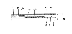
Hereinafter, the best mode for carrying out the present invention will be described with reference to FIGS. In describing the information input device of the present invention, a resistive touch panel (hereinafter simply referred to as a touch panel), which is one of the information input devices, will be described. The same applies to the embodiments described below. Here, FIG. 1 is a plan view of a touch panel according to an embodiment of the present invention, FIG. 2 is a sectional view taken along the line GG in FIG. 1, and FIG. 3 is a plan view of a lower substrate in FIG. Parts having the same configuration as that of the touch panel described in the related art are denoted by the same reference numerals, and the description thereof is limited to the necessary limit.

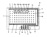
本発明のタッチパネルは固定キー用のアイコン表示をタッチパネルの中に設ける。図1において、一点鎖線で示したDはアクティブエリア(有効操作領域)の範囲を示したもので、一点鎖線Dの中がアクティブエリアになっている。このアクティブエリアは固定キーのアイコンを表示するアイコン表示部領域Eとペン書きで情報が入力できる情報の入出力部領域Fとに分かれている。アイコン表示部領域Eは、切欠部45a、45b、45c、45d、45eを持ったアイコン表示用絶縁膜45が設けられたものから成っていて、このアイコン表示用絶縁膜45はアクティブエリアの縁の領域に設けられる。アイコン表示用絶縁膜45をアクティブエリアの縁領域に設けることによって、情報の入出力部領域Fが広い面積を持って利用できる。切欠部は、その切欠部においてスイッチ動作を行うために設けるものであるから、その切欠部においてスイッチ動作が行える大きさ(広さ)持っている。また更に、切欠部は固定キーのアイコンの種類も示している。図1においては、切欠部は45a、45b、45c、45d、45eの5つを持っており、それぞれの切欠部は、例えば、切欠部45aはアドレスのアイコン、切欠部45bはスケジュールのアイコン、切欠部45cはクリアのアイコン、切欠部45dは△(図形で、進むの意)のアイコン、切欠部45eは▽(図形で、戻るの意)のアイコンなどを示している。この切欠部は文字、記号、図形などによってアイコンの種類が分かる形状に仕上げる。また、アイコン表示用絶縁膜45は不透明になっており、切欠部45a、45b、45c、45d、45eの所は開口されて透明の状態になっている。これによって、それぞれのアイコンがはっきりと区別して視認できるようになっている。図1においては、切欠部を5個設け、5種類のアイコンを示したが、アイコンの数は特に限定するものではなく、必要分設ければ良い。   In the touch panel of the present invention, an icon display for a fixed key is provided in the touch panel. In FIG. 1, D indicated by the alternate long and short dash line indicates the range of the active area (effective operation area), and the inside of the alternate long and short dash line D is the active area. This active area is divided into an icon display area E for displaying fixed key icons and an information input / output area F for inputting information by pen writing. The icon display area E consists of an icon display insulating film 45 having notches 45a, 45b, 45c, 45d, and 45e. The icon display insulating film 45 is formed at the edge of the active area. Provided in the region. By providing the icon display insulating film 45 in the edge area of the active area, the information input / output area F can be used with a large area. Since the notch is provided to perform a switch operation at the notch, the notch has a size (wideness) at which the switch operation can be performed. Furthermore, the notch part also shows the type of the fixed key icon. In FIG. 1, there are five notches 45a, 45b, 45c, 45d, and 45e. For example, the notch 45a has an address icon, the notch 45b has a schedule icon, and a notch. The part 45c shows a clear icon, the notch part 45d shows an icon of Δ (in the figure, meaning to advance), the notch part 45e shows an icon of ▽ (in the figure, means to go back), and the like. This notch is finished in a shape that allows the type of icon to be identified by letters, symbols, figures, and the like. Further, the icon display insulating film 45 is opaque, and the notches 45a, 45b, 45c, 45d, and 45e are opened and are in a transparent state. As a result, each icon can be clearly distinguished and visually recognized. In FIG. 1, five notches are provided and five types of icons are shown. However, the number of icons is not particularly limited and may be provided as necessary.

このような仕様を取るタッチパネル40の構成を説明する。タッチパネル40は上基板11と下基板41とが主要構成部品となって構成される。上基板11は、可撓性のある透明基板12の下面に方形形状に形成した上タッチ電極13と、この上タッチ電極13の対向する二辺に接続してFPC取付部Sに向かって引き回して設けた一対の配線電極14、15と、一対の配線電極14(15)の面上に設けた絶縁膜16(17)とで構成している。下基板41は、図3に示すように、透明基板2の上面に方形形状に形成した下タッチ電極3と、この下タッチ電極3の対向する二辺に接続してFPC取付部Sに向かって引き回して形成した一対の配線電極4、5と、FPC取付部S近辺に形成した接続電極8、9と、下タッチ電極3の上面にマトリックス状に形成したドットスペーサ10と、配線電極4、5の面上に設けた絶縁膜6、7と、下タッチ電極3上あって図3の中で左側の部位に形成した複数の切欠部45a、45b、45c、45d、45eを有するアイコン表示用絶縁膜45とから構成している。アイコン表示用絶縁膜45の下には下タッチ電極3が配設されている。尚以降、上基板並びに下基板の配線電極上に設ける絶縁膜を配線電極用絶縁膜と呼び、アイコン表示用絶縁膜と区別して説明する。   A configuration of the touch panel 40 having such specifications will be described. The touch panel 40 includes an upper substrate 11 and a lower substrate 41 as main components. The upper substrate 11 is connected to two opposing sides of the upper touch electrode 13 formed in a rectangular shape on the lower surface of the flexible transparent substrate 12, and is routed toward the FPC attachment portion S. A pair of wiring electrodes 14 and 15 provided and an insulating film 16 (17) provided on the surface of the pair of wiring electrodes 14 (15). As shown in FIG. 3, the lower substrate 41 is connected to the lower touch electrode 3 formed in a square shape on the upper surface of the transparent substrate 2, and the two opposite sides of the lower touch electrode 3, toward the FPC attachment portion S. A pair of wiring electrodes 4, 5 formed by drawing, connection electrodes 8, 9 formed in the vicinity of the FPC attachment portion S, dot spacers 10 formed in a matrix on the upper surface of the lower touch electrode 3, and wiring electrodes 4, 5 Insulation for icon display having insulating films 6 and 7 provided on the surface and a plurality of notches 45a, 45b, 45c, 45d and 45e formed on the left touch panel in FIG. And a film 45. The lower touch electrode 3 is disposed under the icon display insulating film 45. Hereinafter, the insulating film provided on the wiring electrodes of the upper substrate and the lower substrate is referred to as a wiring electrode insulating film, and will be described separately from the icon display insulating film.

上記の構成を取る上基板11と下基板41と(上基板と下基板を、以降、上下基板と呼ぶこともある)を、ちょうど上基板11の一対の配線電極14、15と下基板41の一対の配線電極4、5とが方形配置となるように配置し、シール材18でもって所定の間隙を設けて上下基板11、41を周回して接着固定してタッチパネル40を仕上げている。また、上下基板11、41を接着固定する時には、同時に、上基板11の一対の配線電極14、15は下基板41に設けた一対の接続電極6、7のそれぞれの先端部で導電性接着剤によって接続される。尚、図示はしていないが、防眩性を高めて透視性や表示品質を良くするために上基板11上面に偏光板、あるいは反射防止膜(ARフィルム)、或いはア
ンチグレアフィルムなどが設けられている。また、下基板41の下面に位相差板を設けている。また、最上位面に偏光板を配設したときには、偏光板の上面には押す操作により偏光板などが損傷するのを防止するためにハードコート膜も設けている。このハードコート膜は、装置の最上位面がタッチパネルの上基板の時には、このタッチパネルの上基板の上面に配設する。また、FPC取付部SにはFPC19が取付いて導通が行われるようになっている。
The upper substrate 11 and the lower substrate 41 having the above-described configuration (the upper substrate and the lower substrate may be referred to as upper and lower substrates hereinafter) are exactly the same as the pair of wiring electrodes 14 and 15 of the upper substrate 11 and the lower substrate 41. The pair of wiring electrodes 4 and 5 are arranged in a square arrangement, and a predetermined gap is provided with the sealing material 18, and the upper and lower substrates 11 and 41 are rotated and bonded and fixed to finish the touch panel 40. When the upper and lower substrates 11 and 41 are bonded and fixed, at the same time, the pair of wiring electrodes 14 and 15 of the upper substrate 11 are electrically conductive adhesives at the respective distal end portions of the pair of connection electrodes 6 and 7 provided on the lower substrate 41. Connected by. Although not shown, a polarizing plate, an antireflection film (AR film), an antiglare film, or the like is provided on the upper surface of the upper substrate 11 in order to improve the antiglare property and improve the transparency and display quality. Yes. In addition, a phase difference plate is provided on the lower surface of the lower substrate 41. Further, when a polarizing plate is provided on the uppermost surface, a hard coat film is also provided on the upper surface of the polarizing plate in order to prevent the polarizing plate and the like from being damaged by the pressing operation. This hard coat film is disposed on the upper surface of the upper substrate of the touch panel when the uppermost surface of the apparatus is the upper substrate of the touch panel. In addition, the FPC 19 is attached to the FPC attachment portion S so as to conduct electricity.

本発明のタッチパネル40の構成は、前述した従来技術のタッチパネル20の構成と比較すると、下基板1にアイコン表示用絶縁膜45を設けられたところが異なる。このアイコン表示用絶縁膜45は、エポキシ樹脂、アクリル樹脂、ウレタン樹脂などの樹脂に顔料などを混ぜ合わせて着色を施してインク化し、スクリーン印刷などの印刷方法で形成する。このアイコン表示用絶縁膜45は、はっきりと視認できることが必要であるので、透過率を下げて不透明にし、着色した色調がはっきり視認できるようにしている。また、このアイコン表示用絶縁膜45は、固定キー用のアイコンを表示するものであるから、切欠部によってアイコンの種類がはっきり識別できるようにしている。従って、前述したように、文字や記号、図形などでアイコンの種類が分かる形状を取る。文字はアイコン表示用絶縁膜45の一部として印刷で形成する。このように、切欠部を文字や記号、図形などで区分け表示を行い、且つ、アイコン表示用絶縁膜45に着色を施すことによってアイコンの種類がはっきりと区分けされて識別でき、押し間違いなどの誤操作を防止する。また、アイコン表示用絶縁膜45の切欠部のない部分には絶縁膜が設けられているので上基板11を押圧してもアイコンのスイッチは入らない。従って、確実な情報入力ができる。   The configuration of the touch panel 40 of the present invention is different from the configuration of the conventional touch panel 20 described above in that the icon display insulating film 45 is provided on the lower substrate 1. The icon display insulating film 45 is formed by mixing a resin such as an epoxy resin, an acrylic resin, or a urethane resin with a pigment or the like to form an ink, which is then formed by a printing method such as screen printing. Since the icon display insulating film 45 needs to be clearly visible, the transmittance is lowered to make it opaque so that the colored tone can be clearly recognized. Further, since the icon display insulating film 45 displays an icon for a fixed key, the type of the icon can be clearly identified by the notch. Therefore, as described above, a shape in which the type of icon can be recognized by characters, symbols, figures, etc. is taken. The characters are formed by printing as a part of the icon display insulating film 45. In this way, the notch part is displayed with characters, symbols, graphics, etc., and the icon display insulating film 45 is colored so that the type of the icon can be clearly distinguished and identified. To prevent. Further, since the insulating film is provided in the portion of the icon display insulating film 45 where there is no notch, the icon is not switched on even if the upper substrate 11 is pressed. Therefore, reliable information input can be performed.

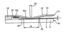
また、アイコン表示用絶縁膜45は、図1に示すように、アクティブエリアの縁領域に形成する。そして、図2に示すように、下基板41の下タッチ電極3上に形成している。尚、下タッチ電極3上にはドットスペーサ10も設けられているので、ドットスペーサ10上にもアイコン表示用絶縁膜45が形成されることにもなる。また、本実施形態では下基板41側に形成したが、これは上基板11の上タッチ電極13上に形成しても良いもので、少なくとも何れか一方側に形成すれば良いものである。アイコン表示用絶縁膜45の切欠部は、その切欠部の所においてスイッチ動作が行える大きさ(広さ)が必要とされる。従って、アイコン表示用絶縁膜45の厚みや、切欠部の大きさはアイコンとしてのスイッチ機能を果たすのに大きく影響を及ぼす。その状態を図4をもって説明する。図4はアイコン表示用絶縁膜の切欠部における働きを説明する説明図を示している。図4において、アイコン表示用絶縁膜45の切欠部45cの上部にある上基板11をペン24で押圧している。可撓性を有する上基板11が撓んで上基板11の上タッチ電極13が下基板41の下タッチ電極3に接触する。tはアイコン表示用絶縁膜45の厚み、mはアイコン表示用絶縁膜45の切欠部45cの幅(大きさ)を表している。ここで、アイコン表示膜45の厚みtが厚すぎると、上基板11の上透明電極13は先にアイコン表示膜45に接触する。このため、上透明電極13を下透明電極3に接触させるためには更なる高い押圧力が必要とされる。このため、押圧力は20〜200gr/cm2 の規定範囲に納まらず、規定外にはみ出してしまうと云う問題が生じる。反面、厚みtが薄いと、上透明電極13はアイコン表示膜45に接触する前に下透明電極3に接触するので低い押圧力で操作することができる。従って、厚みtは薄ければ薄いほど好ましい。本発明においては、アイコン表示用絶縁膜45は配線電極用絶縁膜6、7と一緒にスクリーン印刷方法で印刷形成する。配線電極用絶縁膜6、7は2〜5μmの範囲での薄膜で形成することから、アイコン表示用絶縁膜45は2〜5μmの厚みに形成される。従って、アイコン表示用絶縁膜45の厚みが押圧力に与える影響は非常に小さい。幅mについても同様で、幅mが狭すぎると上下のタッチ電極13、3を接触させるには高い押圧力が必要となる。反面、幅mが広いと低い押圧力で上下のタッチ電極13、3を接触させることができる。従って、幅mは広ければ広いほど好ましいものではある。しかしながら、幅mが広すぎるとアイコン表示用絶縁膜45の面積増大を招き、情報の入出力部領域Fを狭くする。このことから、管理す
る押圧力の範囲の中で上下のタッチ電極13、3が容易に接触し、且つ、求められる入出力部領域の面積が得られる範囲の中で、適宜に切欠部の大きさを設定するのが良い。
Further, the icon display insulating film 45 is formed in the edge area of the active area as shown in FIG. Then, as shown in FIG. 2, the lower substrate 41 is formed on the lower touch electrode 3. Since the dot spacer 10 is also provided on the lower touch electrode 3, the icon display insulating film 45 is also formed on the dot spacer 10. Further, in the present embodiment, it is formed on the lower substrate 41 side, but it may be formed on the upper touch electrode 13 of the upper substrate 11 and may be formed on at least one side. The cutout portion of the icon display insulating film 45 is required to have a size (width) at which the switch operation can be performed at the cutout portion. Accordingly, the thickness of the icon display insulating film 45 and the size of the notch greatly influence the function of the switch as an icon. This state will be described with reference to FIG. FIG. 4 is an explanatory view for explaining the function of the notch portion of the icon display insulating film. In FIG. 4, the upper substrate 11 located above the notch 45 c of the icon display insulating film 45 is pressed with a pen 24. The flexible upper substrate 11 bends and the upper touch electrode 13 of the upper substrate 11 contacts the lower touch electrode 3 of the lower substrate 41. t represents the thickness of the icon display insulating film 45, and m represents the width (size) of the notch 45 c of the icon display insulating film 45. Here, if the thickness t of the icon display film 45 is too thick, the upper transparent electrode 13 of the upper substrate 11 contacts the icon display film 45 first. For this reason, in order to make the upper transparent electrode 13 contact the lower transparent electrode 3, a further higher pressing force is required. For this reason, the pressing force does not fall within the specified range of 20 to 200 gr / cm 2 , causing a problem that the pressing force protrudes outside the specified range. On the other hand, when the thickness t is small, the upper transparent electrode 13 comes into contact with the lower transparent electrode 3 before coming into contact with the icon display film 45, so that it can be operated with a low pressing force. Therefore, the thinner the thickness t, the better. In the present invention, the icon display insulating film 45 is printed and formed together with the wiring electrode insulating films 6 and 7 by a screen printing method. Since the wiring electrode insulating films 6 and 7 are formed as thin films in the range of 2 to 5 μm, the icon display insulating film 45 is formed to a thickness of 2 to 5 μm. Therefore, the influence of the thickness of the icon display insulating film 45 on the pressing force is very small. The same applies to the width m. If the width m is too small, a high pressing force is required to bring the upper and lower touch electrodes 13 and 3 into contact with each other. On the other hand, when the width m is wide, the upper and lower touch electrodes 13 and 3 can be brought into contact with each other with a low pressing force. Accordingly, the wider the width m, the better. However, if the width m is too wide, the area of the icon display insulating film 45 is increased, and the information input / output area F is narrowed. Therefore, the size of the notch portion is appropriately selected within the range in which the upper and lower touch electrodes 13 and 3 can easily come into contact with each other within the range of the pressing force to be managed and the required area of the input / output portion region can be obtained. It is good to set.

本発明は、以上説明したように、タッチパネルが持っているスイッチ機能を利用してアイコン表示をタッチパネルの中に設け、アイコン表示の中にスイッチ機能を持たせた構成を取る。即ち、切欠部を有するアイコン表示用絶縁膜をタッチパネルの中に設け、その切欠部の大きさを切欠部の中でスイッチ動作が行える大きさに設定し、その切欠部の中でスイッチ動作を行う構成にしている。また、アイコン表示はその種類なども含めて明確に視認できるようにするために、アイコン表示に着色などを施して不透明にし、更に、切欠部を文字や記号、図形などでアイコンの種類が分かる形状にしている。このような構成を取ることによって、アイコンの種類がすぐ見分けられ、スピーディに正確に情報入力ができるようになる。また、従来技術で説明したように、別途にアイコン表示を設けたスペーサなどの部品を用意する必要はなくなり、部品コスト、組立コストの低減効果が得られる。   As described above, the present invention employs a configuration in which an icon display is provided in the touch panel using the switch function of the touch panel, and the switch function is provided in the icon display. That is, an icon display insulating film having a notch is provided in the touch panel, the size of the notch is set to a size that allows a switch operation in the notch, and the switch operation is performed in the notch. It has a configuration. In order to make the icon display clearly visible, including its type, the icon display is colored to make it opaque, and the notch is shaped so that the type of icon can be seen with characters, symbols, figures, etc. I have to. By adopting such a configuration, the types of icons can be identified immediately, and information can be input quickly and accurately. Further, as described in the related art, it is not necessary to prepare a component such as a spacer provided with an icon display separately, and an effect of reducing component cost and assembly cost can be obtained.

次に、上記の構成を取るタッチパネル40の製造方法を説明する。最初に下基板41について、ガラスからなる透明基板2に透明なる下タッチ電極3を形成する。下タッチ電極3は、真空蒸着法などでITO膜を形成し、その後にフォトリソグラフィにより不要なITO膜を除去し、所要の寸法のITO膜にしてタッチ電極にする。次に、下タッチ電極3上にスクリーン印刷などの印刷方法でドットスペーサ10を印刷形成し、その後に加熱処理又は紫外線照射によってドットスペーサ10を硬化する。次に、一対の配線電極4、5及び一対の接続電極8、9を銀ペーストを用いてスクリーン印刷などのマスクを用いた印刷方法で形成し、加熱処理を施して硬化させる。
このとき、印刷マスクには、絶縁膜の切り欠き部となるところには、マスクで覆われ、絶縁膜で光を遮るあるいは透過を抑制する部分は絶縁膜がタッチパネル基板上に配設されるようにメッシュ状に加工されたマスクを用いる。
次に、アイコン表示用絶縁膜45と配線電極用絶縁膜6、7をスクリーン印刷などの印刷方法で形成し、加熱処理を施して硬化させる。これによって下基板41ができあがる。次に、上基板11について、薄板ガラスまたは樹脂フィルムからなる透明基板12に透明な上タッチ電極13を形成する。この上タッチ電極13は、下タッチ電極3と同様に、真空蒸着法などでITO膜を形成し、その後にフォトリソグラフィにより不要なITO膜を除去して形成する。次に、一対の配線電極14、15を銀ペーストを用いてスクリーン印刷などの印刷方法で印刷形成し、その後、加熱処理を施して硬化させる。次に、一対の配線電極14、15の必要部分に配線電極用絶縁膜16、17をスクリーン印刷などの印刷方法で形成し、加熱処理を施して硬化させる。これによって上基板11ができあがる。
Next, a method for manufacturing the touch panel 40 having the above configuration will be described. First, for the lower substrate 41, the transparent lower touch electrode 3 is formed on the transparent substrate 2 made of glass. As the lower touch electrode 3, an ITO film is formed by a vacuum deposition method or the like, and then an unnecessary ITO film is removed by photolithography to form an ITO film having a required size to be a touch electrode. Next, the dot spacer 10 is printed and formed on the lower touch electrode 3 by a printing method such as screen printing, and then the dot spacer 10 is cured by heat treatment or ultraviolet irradiation. Next, the pair of wiring electrodes 4 and 5 and the pair of connection electrodes 8 and 9 are formed using a silver paste by a printing method using a mask such as screen printing, and subjected to heat treatment to be cured.
At this time, the printed mask is covered with a mask where the insulating film is notched, and the insulating film is disposed on the touch panel substrate where light is blocked or suppressed by the insulating film. A mask processed into a mesh shape is used.
Next, the icon display insulating film 45 and the wiring electrode insulating films 6 and 7 are formed by a printing method such as screen printing, and are cured by heat treatment. As a result, the lower substrate 41 is completed. Next, with respect to the upper substrate 11, a transparent upper touch electrode 13 is formed on the transparent substrate 12 made of thin glass or a resin film. As with the lower touch electrode 3, the upper touch electrode 13 is formed by forming an ITO film by a vacuum deposition method or the like and then removing an unnecessary ITO film by photolithography. Next, the pair of wiring electrodes 14 and 15 are formed by printing using a silver paste by a printing method such as screen printing, and then subjected to heat treatment to be cured. Next, the wiring electrode insulating films 16 and 17 are formed on necessary portions of the pair of wiring electrodes 14 and 15 by a printing method such as screen printing, and are cured by heat treatment. As a result, the upper substrate 11 is completed.

このように本発明は、タッチ電極と前記タッチ電極と接続された配線電極を有する上基板とタッチ電極と前記タッチ電極と接続された配線電極を有する配線電極を有する下基板とを一定の間隙を設けて電極を対向させて配置し前記間隙の周辺にシール材を配設した情報入力装置の製造方法が、前記上下基板の少なくとも一方の基板の前記タッチ電極上の一部分に絶縁膜を配設工程で、前記絶縁膜に光透過切欠部を形成するための形状をなすマスクを用いて前記絶縁膜を印刷する絶縁膜印刷工程を有することを特徴とし、さらに前記絶縁膜を印刷する工程で、該絶縁膜を印刷する側の基板で前記配線電極の面上に形成する配線電極用絶縁膜にも同時に印刷するマスクを用いて印刷することを特徴とする製造工程を有する。   As described above, the present invention provides a fixed gap between the upper substrate having the touch electrode and the wiring electrode connected to the touch electrode, and the lower substrate having the wiring electrode having the wiring electrode connected to the touch electrode. A method of manufacturing an information input device in which an electrode is provided so as to face each other and a sealing material is provided around the gap, and an insulating film is provided on a part of the touch electrode of at least one of the upper and lower substrates. The insulating film printing step of printing the insulating film using a mask having a shape for forming a light transmissive notch in the insulating film, and further comprising the step of printing the insulating film, A wiring electrode insulating film formed on the surface of the wiring electrode on the substrate on which the insulating film is printed is printed using a mask that simultaneously prints.

次に、上基板11または下基板41の何れか一方にシール材18をスクリーン印刷などの印刷方法で形成する。そして、低温(80°〜100°C)で仮硬化させる。次に上基板11と下基板41を対向させて位置を合わせ、何枚かを積み重ねて加圧装置にセットし、セットした加圧装置を焼成炉に入れて、加圧力と加熱温度を段階的に高めて、最後は150°〜180°Cの加熱温度で焼成する。これによって、シール材18を完全に硬化し
て上基板11と下基板41とが接着固定される。尚、上基板11の一対の配線電極14、15と下基板41の一対の接続電極6、7との接続は、下基板41の接続電極6、7の先端部に導電性接着剤を塗布しておくことにより、上基板11と下基板41を対向させて位置を合わせて加圧・加熱処理を行ったときに導電性接着剤が硬化して接続するようになっている。これによってタッチパネル40が得られる。
Next, the sealing material 18 is formed on either the upper substrate 11 or the lower substrate 41 by a printing method such as screen printing. And it makes it harden | cure at low temperature (80-100 degreeC). Next, the upper substrate 11 and the lower substrate 41 are made to face each other, aligned, and several sheets are stacked and set in a pressurizing apparatus. The set pressurizing apparatus is put in a firing furnace, and the applied pressure and heating temperature are stepped. Finally, baking is performed at a heating temperature of 150 ° to 180 ° C. As a result, the sealing material 18 is completely cured and the upper substrate 11 and the lower substrate 41 are bonded and fixed. The connection between the pair of wiring electrodes 14 and 15 on the upper substrate 11 and the pair of connection electrodes 6 and 7 on the lower substrate 41 is performed by applying a conductive adhesive to the tips of the connection electrodes 6 and 7 on the lower substrate 41. Thus, the conductive adhesive is cured and connected when the pressing and heating processes are performed with the upper substrate 11 and the lower substrate 41 facing each other. Thereby, the touch panel 40 is obtained.

アイコン表示用絶縁膜45は、アイコン表示用絶縁膜の印刷形状と配線電極用絶縁膜の印刷形状とが盛り込まれたスクリーン印刷版を用いてスクリーン印刷し、配線電極用絶縁膜も一緒に形成する。印刷作業は比較的簡単で、且つ、品質精度が得られること、アイコン表示用絶縁膜45と配線電極用絶縁膜とが1回の印刷回数で同時に印刷できることなどから、印刷コストも安く上がり、アイコン表示用絶縁膜45の切欠部の寸法なども高い精度のものを得ることができる。   The icon display insulating film 45 is screen-printed using a screen printing plate in which the printed shape of the icon display insulating film and the printed shape of the wiring electrode insulating film are incorporated, and the wiring electrode insulating film is also formed together. . The printing operation is relatively easy and quality accuracy is obtained, and the icon display insulating film 45 and the wiring electrode insulating film can be printed at the same time in one printing operation. It is possible to obtain a high-accuracy dimension of the notch portion of the display insulating film 45.

このように本発明は、タッチ電極と前記タッチ電極と接続された配線電極を有する上基板とタッチ電極と前記タッチ電極と接続された配線電極を有する配線電極を有する下基板とを一定の間隙を設けて電極を対向させて配置し前記間隙の周辺にシール材を配設した情報入力装置において、前記上下基板の少なくとも一方の基板の前記タッチ電極上の一部分に光透過を抑止あるいは遮る絶縁膜を設け、前記絶縁膜の面に光透過が透過する切欠部を設けたことを特徴とし、前記絶縁膜の前記切欠部の形状が、文字や記号、図形、絵柄を成していることを特徴としている。
この絶縁膜により、タッチパネルのアイコン表示として用いることができると共に、アイコン部分でタッチパネルのスイッチをオン−オフ切り替えるようにすることもできる。
アイコン以外の表示部としても応用ができる。例えば、犬の絵、キャラクターを絶縁膜で表示することができる応用効果を有す。
As described above, the present invention provides a fixed gap between the upper substrate having the touch electrode and the wiring electrode connected to the touch electrode, and the lower substrate having the wiring electrode having the wiring electrode connected to the touch electrode. In an information input device provided and arranged with electrodes facing each other and a sealant disposed around the gap, an insulating film that inhibits or blocks light transmission is provided on a part of the touch electrode of at least one of the upper and lower substrates. The insulating film is provided with a cutout portion through which light is transmitted, and the shape of the cutout portion of the insulating film is a character, symbol, figure, or pattern. Yes.
With this insulating film, it can be used as an icon display of the touch panel, and the touch panel switch can be switched on and off at the icon portion.
It can also be applied as a display unit other than icons. For example, it has an application effect that can display a picture or character of a dog with an insulating film.

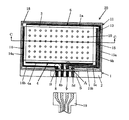
本発明の実施例1として、タッチパネルの下面側に液晶表示装置とバックライトを備えた画面入力型表示装置を図5を用いて説明する。図5は本発明の実施例1に係る画面入力型表示装置を示したもので、図5の(a)は平面図、図5の(b)は要部分の断面を盛り込んだ側面図である。     As Example 1 of the present invention, a screen input type display device including a liquid crystal display device and a backlight on the lower surface side of a touch panel will be described with reference to FIG. FIGS. 5A and 5B show a screen input type display device according to the first embodiment of the present invention. FIG. 5A is a plan view, and FIG. 5B is a side view including a cross section of a main part. .

図5において、最上層部にはタッチパネルが配置されている。このタッチパネルは前述の実施の形態で説明した構成のタッチパネル40を用いている。このタッチパネル40の構成は前述の実施の形態の中で詳しく説明しているのでここでの説明は必要限度に留める。このタッチパネル40は、アクティブエリア内に固定キーのアイコンを表示するアイコン表示部領域E(図5(a)の中で左端側)と、ペン書きや人の指で情報が入力できる情報の入出力部領域Fを持っている。アイコン表示部領域Eには前述の図1を用いて説明した複数の切欠部を持ったアイコン表示用絶縁膜45が形成されている。また、このアイコン表示用絶縁膜45の幅はnの寸法を持っている。このタッチパネル40は支持固定枠58によって支持されている。   In FIG. 5, a touch panel is arranged on the uppermost layer. This touch panel uses the touch panel 40 having the configuration described in the above embodiment. Since the configuration of the touch panel 40 has been described in detail in the above-described embodiment, the description here is limited to the necessary limit. The touch panel 40 has an icon display area E (the left end side in FIG. 5A) that displays a fixed key icon in the active area, and input / output of information that can be input by pen writing or a human finger. It has a partial area F. In the icon display area E, an icon display insulating film 45 having a plurality of notches described with reference to FIG. 1 is formed. Further, the width of the icon display insulating film 45 is n. The touch panel 40 is supported by a support fixing frame 58.

タッチパネル40の下面側には液晶表示装置50が配設され、両面接着テープ51によってタッチパネル40と液晶表示装置50とが所定の間隙を持って固定されている。液晶表示装置50の下には半透過反射層52があり、更にその下に、バックライトを構成するところの光の拡散層56と導光板55とが積層し、導光板55の横(図5(b)の中で右端側)にはLEDなどからなる光源57が設けられている。そして、これらの部品を内蔵する形で支持固定枠58で支持固定している。尚、図5(b)においては、タッチパネル40や液晶表示装置50に取付く駆動基板との接続ケーブル(FPCなど)は省略してある。   A liquid crystal display device 50 is disposed on the lower surface side of the touch panel 40, and the touch panel 40 and the liquid crystal display device 50 are fixed with a predetermined gap by a double-sided adhesive tape 51. A transflective layer 52 is provided below the liquid crystal display device 50, and a light diffusing layer 56 and a light guide plate 55 constituting a backlight are laminated below the liquid crystal display device 50. Next to the light guide plate 55 (FIG. 5). A light source 57 made of an LED or the like is provided on the right end side in (b). Then, these components are supported and fixed by a support fixing frame 58 in a built-in form. In FIG. 5B, a connection cable (FPC or the like) to the drive board attached to the touch panel 40 or the liquid crystal display device 50 is omitted.

ここで、液晶表示装置50の幅lはタッチパネル40の情報の入出力部領域Fの部分を表示するぐらいの幅しか持っていない。即ち、アイコン表示用絶縁膜45を設けたところのアイコン表示部領域Eの下方には液晶表示装置50はなく、アイコン表示用絶縁膜45の部分は直接導光板55から放射される光でもって照明するようになっている。これは、固定キー用のアイコン表示はタッチパネル40に設けたアイコン表示用絶縁膜45で行っているので、液晶表示は必要とせず、アイコン表示を照明する光だけがあれば良いことによる。一般に、タッチパネルの下に配設する液晶表示装置はタッチパネルの大きさと同じ位の大きさを取っている。また、バックライトを構成するところの導光板も同様である。しかしながら、本発明の画面入力型表示装置においては、液晶表示装置50はアイコン表示用絶縁膜45の幅nに相当する分の幅を縮めて幅を狭くしてあり、そして、情報の入出力部領域Fの部分を表示できる大きさにしてある。このような構成を取ることによって、液晶表示装置の小型化が図れて材料コストの低減ができる。更に、タッチパネルに設けたアイコン表示は直接バックライトの光で照明するので非常に明るい。液晶表示装置と半透過反射膜を介した照明は透過率がだいぶ低くなるので照明明るさは相当低下する。本発明の構成ではこの問題は解消される。     Here, the width l of the liquid crystal display device 50 has a width enough to display the information input / output area F of the touch panel 40. That is, there is no liquid crystal display device 50 below the icon display area E where the icon display insulating film 45 is provided, and the portion of the icon display insulating film 45 is illuminated with light directly emitted from the light guide plate 55. It is supposed to be. This is because the icon display for the fixed key is performed by the icon display insulating film 45 provided on the touch panel 40, so that the liquid crystal display is not required and only the light for illuminating the icon display is required. In general, the liquid crystal display device disposed under the touch panel is as large as the touch panel. The same applies to the light guide plate constituting the backlight. However, in the screen input type display device of the present invention, the liquid crystal display device 50 is narrowed by reducing the width corresponding to the width n of the icon display insulating film 45, and the information input / output unit. The size of the area F can be displayed. By adopting such a configuration, the liquid crystal display device can be miniaturized and the material cost can be reduced. Furthermore, the icon display provided on the touch panel is very bright because it is directly illuminated by backlight light. Since the illumination through the liquid crystal display device and the semi-transmissive reflective film has a considerably low transmittance, the illumination brightness is considerably reduced. This problem is solved by the configuration of the present invention.

また、本発明の画面入力型表示装置においては、固定キー用のアイコン表示はタッチパネル40に設けている。従って、従来技術で用いられていたスペーサなる特別な部品は必要とせず、組み付ける作業も不要としている。部品コスト低減と組立コストの低減効果が得られる。更にまた、従来技術で用いられていたスペーサスが不要となることから、その分薄型化の効果も得られる。また、タッチパネルに設ける固定キー用のアイコン表示は切欠部を設けたアイコン表示用絶縁膜で行う。従来行っている配線電極用絶縁膜の印刷形成のときにこのアイコン表示用絶縁膜の印刷も一緒に行うことができるので、印刷コストを変えることなくアイコン表示ができる。   In the screen input type display device of the present invention, the icon display for the fixed key is provided on the touch panel 40. Therefore, a special part such as a spacer used in the prior art is not required, and an assembling work is also unnecessary. Parts cost and assembly cost can be reduced. Furthermore, since the spacers used in the prior art are not necessary, the effect of reducing the thickness can be obtained. Further, the icon display for the fixed key provided on the touch panel is performed with an icon display insulating film provided with a notch. Since the icon display insulating film can be printed together with the conventional wiring electrode insulating film printing, the icon can be displayed without changing the printing cost.

本実施例1においては、タッチパネル40の上基板11の透明基板12はPETフィルムを用い、上下基板11、41の間隙(ギャップ)量は100μm位に設定してある。そして、下基板41に設けたアイコン表示用絶縁膜45は黒色に着色した樹脂インクを用い配線電極用絶縁膜と一緒にスクリーン印刷方法で厚み2〜5μmの範囲に形成している。従って、切欠部でもって構成したアイコン表示部はコントラストが高められ、アイコン表示がはっきりと視認され、切欠部のそれぞれの形状によってアイコンの種類が明確に区別して視認できる。尚、アイコン表示用絶縁膜45を黒色で形成することで配線電極用絶縁膜も黒色となるが、この配線電極の部分は外観部分として見えない位置に支持固定枠部材に組付けるので支障は生じない。
In the first embodiment, the transparent substrate 12 of the upper substrate 11 of the touch panel 40 uses a PET film, and the gap (gap) amount between the upper and lower substrates 11 and 41 is set to about 100 μm. The icon display insulating film 45 provided on the lower substrate 41 is formed in a thickness of 2 to 5 μm by a screen printing method together with the wiring electrode insulating film using a resin ink colored in black. Therefore, the icon display part constituted by the notch part is enhanced in contrast, the icon display is clearly recognized, and the icon type can be clearly distinguished and recognized by the shape of each notch part. By forming the icon display insulating film 45 in black, the wiring electrode insulating film also becomes black. However, this wiring electrode portion is attached to the support fixing frame member at a position where it cannot be seen as an appearance portion, and thus troubles occur. Absent.

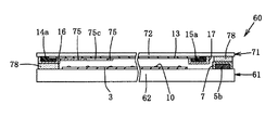
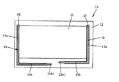
次に、図6、図7を用いて本発明の実施例2を説明する。図6は本発明の実施例2に係るタッチパネルの要部断面図を示しており、図7は図6における上基板の平面図を示している。最初に、実施例2におけるタッチパネル60の構成を説明する。実施例2のタッチパネル60も、図6に示すように、上基板71と下基板61とが主要構成部品となって構成する。そして、従来技術で説明したタッチパネル20と相違するところの第1点目は、一番外側に位置する配線電極のところにシール材78を配設し、上下基板71、61を貼合わせたところである。従来技術におけるのタッチパネル20は配線電極の外側部分で上下基板を貼合わせていた。従って、実施例2におけるタッチパネル60は従来技術のものより小型になっている。即ち、上基板71の透明基板72、及び下基板61の透明基板62は従来技術のものより大きさが少し小さいものを使用している。次に、相違するところの第2点目は、固定キー用のアイコンを表示するために切欠部を有するアイコン表示用絶縁膜75を設けてあるところである。   Next, Embodiment 2 of the present invention will be described with reference to FIGS. 6 shows a cross-sectional view of the main part of the touch panel according to Embodiment 2 of the present invention, and FIG. 7 shows a plan view of the upper substrate in FIG. First, the configuration of the touch panel 60 in the second embodiment will be described. As shown in FIG. 6, the touch panel 60 of the second embodiment also includes an upper substrate 71 and a lower substrate 61 as main components. And the 1st point different from the touch panel 20 demonstrated by the prior art is the place which has arrange | positioned the sealing material 78 in the place of the wiring electrode located in the outermost side, and bonded the upper and lower substrates 71 and 61 together. . In the touch panel 20 in the prior art, the upper and lower substrates are bonded to each other at the outer portion of the wiring electrode. Therefore, the touch panel 60 in the second embodiment is smaller than that of the prior art. That is, the transparent substrate 72 of the upper substrate 71 and the transparent substrate 62 of the lower substrate 61 are slightly smaller in size than those of the prior art. Next, the second difference is that an icon display insulating film 75 having a notch is provided in order to display a fixed key icon.

次に、以下に実施例2のタッチパネル60を詳しく説明する。上基板71は、図7に示すように、可撓性のある透明基板72の下面に方形形状に形成した上タッチ電極13と、この上タッチ電極13の対向する二辺に接続してFPC取付部Sに向かって引き回して設けた一対の配線電極14、15と、一対の配線電極14、15の面上に設けた配線電極用絶縁膜16、17と、図7の中で左端側に設けた切欠部を有するアイコン表示用絶縁膜75とから構成している。ここでのアイコン表示用絶縁膜75は、配線電極14aの面上に設けた配線電極用絶縁膜16を延設して形成し、この延設部分をアイコン表示用絶縁膜75としたものである。配線電極14は、従来技術と同様に、電極14a部分と電極14b部分を持っており、配線電極15も15a部分と15b部分を持っている。アイコン表示用絶縁膜75は、配線電極14a部分に設けた配線電極用絶縁膜16を横に延設して広げ、この広げた部分をアイコン表示用絶縁膜75としている。従って、アイコン表示用絶縁膜75は配線電極用絶縁膜16と同じ材料で同一工程で形成している。アイコン表示用絶縁膜75は切欠部75a、75b、75c、75d、75eを持っていて、この切欠部75a、75b、75c、75d、75eの形状などによって固定キー用のアイコンの種類を表示している。切欠部の形状は文字や記号、図形などを用いてそれぞれのアイコンの種類がはっきり区別できるような形状を取っている。また、これらの切欠部は何れもアクティブエリア内に納まる位置に設けている。   Next, the touch panel 60 of Example 2 will be described in detail below. As shown in FIG. 7, the upper substrate 71 is connected to two opposite sides of the upper touch electrode 13 formed in a rectangular shape on the lower surface of the flexible transparent substrate 72 and attached to the FPC. A pair of wiring electrodes 14 and 15 provided by being routed toward the portion S, wiring electrode insulating films 16 and 17 provided on the surfaces of the pair of wiring electrodes 14 and 15, and provided on the left end side in FIG. And an icon display insulating film 75 having a notch. The icon display insulating film 75 is formed by extending the wiring electrode insulating film 16 provided on the surface of the wiring electrode 14a, and this extended portion is used as the icon display insulating film 75. . Similar to the prior art, the wiring electrode 14 has an electrode 14a portion and an electrode 14b portion, and the wiring electrode 15 also has a 15a portion and a 15b portion. The insulating film 75 for icon display is formed by extending the wiring electrode insulating film 16 provided in the wiring electrode 14a sideways, and this expanded part is used as the insulating film 75 for icon display. Therefore, the icon display insulating film 75 is formed of the same material and in the same process as the wiring electrode insulating film 16. The icon display insulating film 75 has cutout portions 75a, 75b, 75c, 75d, and 75e, and displays the type of icon for the fixed key depending on the shape of the cutout portions 75a, 75b, 75c, 75d, and 75e. Yes. The shape of the notch is such that the type of each icon can be clearly distinguished using characters, symbols, figures, and the like. In addition, these notches are provided at positions that fit within the active area.

さらに、図3を参照しながら図6,7の説明を行う。
下基板61は透明基板62の上面に、図3で示されたところの方形形状に形成した下タッチ電極3と、この下タッチ電極3の対向する二辺に接続してFPC取付部Sに向かって引き回して形成した一対の配線電極4、5と、FPC取付部S近辺に形成した接続電極8、9と、下タッチ電極3の上面にマトリックス状に形成したドットスペーサ10と、配線電極4、5の面上に設けた絶縁膜6、7とで構成している。配線電極4、5はFPC取付部Sに向かって引き回しているため、配線電極4は電極4a部分と4b部分を持ち、同様に、配線電極5も5a、5b、5c、5d部分を持っている。図6においては、配線電極5は5b部分のみが描かれている。
Further, FIGS. 6 and 7 will be described with reference to FIG.
The lower substrate 61 is connected to the lower touch electrode 3 formed in the rectangular shape shown in FIG. 3 on the upper surface of the transparent substrate 62 and to the two opposite sides of the lower touch electrode 3 toward the FPC mounting portion S. A pair of wiring electrodes 4, 5 formed by drawing, connection electrodes 8, 9 formed in the vicinity of the FPC attachment portion S, dot spacers 10 formed in a matrix on the upper surface of the lower touch electrode 3, wiring electrodes 4, Insulating films 6 and 7 provided on the surface 5. Since the wiring electrodes 4 and 5 are routed toward the FPC mounting portion S, the wiring electrode 4 has an electrode 4a portion and a 4b portion, and similarly, the wiring electrode 5 also has a 5a, 5b, 5c, and 5d portion. . In FIG. 6, only the 5b portion is drawn on the wiring electrode 5.

上記の構成を取る上基板71と下基板61とを対向配置して所定の間隙を設けてシール材78で接着固定する。シール材78は上下基板71、61の何れか一方に印刷形成するが、これは、上下基板71、61のそれぞれの配線電極の一番外側に当たる電極の部位に重なって印刷される。上下基板71、61の接着固定方法は前述の本発明の実施形態で説明した加圧装置と焼成炉を用いて同じ方法で行う。本実施例2では、上基板71の透明基板72にPETフィルムを用い、上下基板71、61の間隙量が100μmになるようにシール材78で接着固定している。尚、上基板71と下基板61とを接着固定する時に、同時に、上基板71の一対の配線電極14、15は下基板61に設けた一対の接続電極8、9のそれぞれの先端部で導電性接着剤によって接続する。     The upper substrate 71 and the lower substrate 61 having the above-described configuration are arranged to face each other, a predetermined gap is provided, and the adhesive is fixed by a sealing material 78. The sealing material 78 is formed by printing on either one of the upper and lower substrates 71 and 61, which is printed so as to overlap with the electrode portion corresponding to the outermost side of the respective wiring electrodes of the upper and lower substrates 71 and 61. The upper and lower substrates 71 and 61 are bonded and fixed by the same method using the pressurizing apparatus and the firing furnace described in the embodiment of the present invention. In the second embodiment, a PET film is used for the transparent substrate 72 of the upper substrate 71, and the upper and lower substrates 71 and 61 are bonded and fixed with a sealing material 78 so that the gap amount is 100 μm. At the same time, when the upper substrate 71 and the lower substrate 61 are bonded and fixed, the pair of wiring electrodes 14 and 15 of the upper substrate 71 are electrically conductive at the respective tip portions of the pair of connection electrodes 8 and 9 provided on the lower substrate 61. Connect with adhesive.

アイコン表示用絶縁膜75は、配線電極用絶縁膜16を延設して形成しているが、着色を施して透過率を低くして不透明にする。本実施例2においては、アイコン表示用絶縁膜75を配線電極用絶縁膜と共に、黒色に着色した絶縁インクを用いてスクリーン印刷方法で2〜5μmの厚みに形成している。このようにするとアイコン表示用絶縁膜75がはっきりと視認できる。また、アイコン表示用絶縁膜75の切欠部は、切欠部の中で上基板71の上タッチ電極13と下基板61の下タッチ電極3とを接触させてスイッチ動作を行わせるところなので、上タッチ電極13と下タッチ電極3との接触動作が行える大きさに形成している。そして、その大きさの下で、文字や記号、図形などを用いてアイコンの種類がはっきり区別できる表示形状を取っている。このようにすると、アイコンがはっきりと視認できると共にその種類もはっきりと区別して視認できる。そして、切欠部の所でスイッチ動作が行える。   The icon display insulating film 75 is formed by extending the wiring electrode insulating film 16. However, the icon display insulating film 75 is colored to make the transmittance low and opaque. In the second embodiment, the icon display insulating film 75 is formed together with the wiring electrode insulating film to a thickness of 2 to 5 μm by a screen printing method using an insulating ink colored in black. Thus, the icon display insulating film 75 can be clearly seen. Further, the notch portion of the icon display insulating film 75 is a place where the upper touch electrode 13 of the upper substrate 71 and the lower touch electrode 3 of the lower substrate 61 are brought into contact with each other in the notch portion to perform a switch operation. The electrode 13 and the lower touch electrode 3 are formed in a size that allows contact operation. Under the size, a display shape is used in which the types of icons can be clearly distinguished using characters, symbols, figures, and the like. In this way, the icon can be clearly recognized and the type can be clearly distinguished and visually recognized. A switch operation can be performed at the notch.

また、アイコン表示用絶縁膜75は配線電極用絶縁膜16と同じ材料で、双方同時に印刷形成する。印刷はスクリーン印刷方法などを取るが、用いる印刷版はアイコン表示用絶縁膜75と配線電極用絶縁膜16、17の印刷形状を両方盛り込んだ印刷版を用いている。
このようにすると同時印刷が可能となり、印刷コストは同じコストで済む。
Further, the icon display insulating film 75 is made of the same material as the wiring electrode insulating film 16, and both are printed and formed simultaneously. For printing, a screen printing method or the like is used. As a printing plate to be used, a printing plate including both the icon display insulating film 75 and the wiring electrode insulating films 16 and 17 is used.
In this way, simultaneous printing is possible, and the printing cost is the same.

上記構成のタッチパネル60を液晶表示装置の上面側に配設して画面入力型表示装置に用いることができる。本実施例2のタッチパネル60を用いて前述の実施例1で説明した構成の画面入力型表示装置を形成すると、実施例1で説明したところの効果、即ち、部品コスト、組立コストの低減、薄型化、液晶表示装置の小型化、アイコン表示の明るい照明などの効果を得る。
The touch panel 60 having the above configuration can be disposed on the upper surface side of the liquid crystal display device and used for a screen input type display device. When the screen input type display device having the configuration described in the first embodiment is formed by using the touch panel 60 of the second embodiment, the effects described in the first embodiment, that is, the cost of parts, the assembly cost is reduced, and the thickness is reduced. Effects such as downsizing, downsizing of liquid crystal display device, bright illumination of icon display, etc. are obtained.

次に、本発明の実施例3を図8〜図11を用いて説明する。ここで、図8は実施例3におけるタッチパネルの平面図、図9は図8におけるH−H断面図、図10は図8における下基板の平面図、図11は図8における上基板の平面図を示したものである。実施例3のタッチパネルはレストランなどの食堂でお客様からの注文を受けるときに用いるハンディタイプの画面入力型装置に備えるタッチパネルである。先ず、実施例3におけるタッチパネルの入力画面を図8を用いて説明する。図8の中で左側に注文を受ける操作の手順などを示す固定キー用のアイコン表示部がある。この表示部は切欠部を持った第1のアイコン表示用絶縁膜95でもって形成されている。図8においては、食事テーブル番号を設定するところのアイコンを示す切欠部95a、画面表示を進めるところのアイコンを示す切欠部95b、画面表示を戻すところのアイコンを示す切欠部95c、間違いや変更などにより入力指示を取り消すところのアイコンを示す切欠部95d、注文品目が全て決まって注文確定を指示するアイコンを示す切欠部95eが設けられている。図8の中で上側には、食べ物の種類を示す固定キー用のアイコン表示部がある。このアイコン表示部は食べ物をジャンル別に大別してのアイコン表示をなしている。この食べ物の種類を示すアイコン表示部は切欠部を持った第2のアイコン表示用絶縁膜85でもって形成されている。図8においては、うどんやそば、ラーメンなどの麺類のアイコンを示す切欠部85a、丼物のアイコンを示す切欠部95b、定食のアイコンを示す切欠部85c、単品品目のアイコン示す切欠部85d、飲物のアイコンを示す切欠部85eが設けられている。ここで、第1のアイコン表示用絶縁膜95の各切欠部、及び第2のアイコン表示用絶縁膜85の各切欠部は、図8の中で一点鎖線Dで示すアクティブエリア内にあって、この切欠部のところでアイコンのスイッチ動作が行える大きさに形成している。そして、この切欠部のところを押圧して操作を行うようになっている。また、これらの切欠部は操作の手順などを示すアイコン表示部、食べ物の種類を示すアイコン表示部以外の部分は大きく2つの領域(J、K)に区分けされている。Jの領域はテーブルの各番号、麺類の各種メニュー、丼物の各種メニュー、定食の各種メニューなどが表示されるようになっていて、表示されたメニューをペンや指で押圧することによって注文メニューが設定できるようになっている。また、Kの領域は、テーブル番号、注文されたメニューの品目、価格などが表示されるようになっている。Jの領域で表示される数多くのメニュー品目の表示やKの領域で表示される注文メニュー品目の表示は、このタッチパネル80の下面側に配設した液晶表示装置によって表示され、透明なタッチパネル80を介して視認する。   Next, a third embodiment of the present invention will be described with reference to FIGS. 8 is a plan view of the touch panel in Example 3, FIG. 9 is a cross-sectional view taken along the line HH in FIG. 8, FIG. 10 is a plan view of the lower substrate in FIG. 8, and FIG. Is shown. The touch panel of Example 3 is a touch panel provided in a handy type screen input type device used when receiving an order from a customer at a restaurant such as a restaurant. First, a touch panel input screen according to the third embodiment will be described with reference to FIG. On the left side of FIG. 8, there is an icon display section for a fixed key indicating an operation procedure for receiving an order. This display portion is formed of a first icon display insulating film 95 having a notch. In FIG. 8, a cutout portion 95a indicating an icon for setting a meal table number, a cutout portion 95b indicating an icon for advancing the screen display, a cutout portion 95c indicating an icon for returning the screen display, an error or a change, etc. Are provided with a notch portion 95d indicating an icon for canceling the input instruction, and a notch portion 95e indicating an icon for instructing order confirmation when all the order items are determined. In the upper side of FIG. 8, there is an icon display portion for a fixed key indicating the type of food. This icon display unit displays icons by roughly classifying food by genre. The icon display portion indicating the type of food is formed of a second icon display insulating film 85 having a notch. In FIG. 8, a cutout portion 85a showing icons for noodles such as udon, soba and ramen, a cutout portion 95b showing a bowl icon, a cutout portion 85c showing a set meal icon, a cutout portion 85d showing a single item icon, a drink Is provided with a notch 85e. Here, each notch portion of the first icon display insulating film 95 and each notch portion of the second icon display insulating film 85 are within the active area indicated by the alternate long and short dash line D in FIG. The size of the cutout is such that the icon can be switched. And operation is performed by pressing the notch. Further, these cutout portions are roughly divided into two regions (J, K) except for an icon display portion indicating an operation procedure and an icon display portion indicating the type of food. In the area of J, various table numbers, various menus for noodles, various menus for bowls, various menus for set meals, etc. are displayed. By pressing the displayed menu with a pen or finger, an order menu is displayed. Can be set. In the area K, the table number, ordered menu item, price, and the like are displayed. The display of many menu items displayed in the area of J and the display of the order menu items displayed in the area of K are displayed by a liquid crystal display device disposed on the lower surface side of the touch panel 80. To see through.

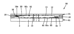
次に、このタッチパネル80の構成を図9、図10、図11を用いて説明する。このタッチパネル80は上基板と下基板とが主要構成部品となって構成している。上基板91は、図11に示すように、上基板91に第1のアイコン表示用絶縁膜95を設けた構成になっている。即ち、可撓性のある透明基板12の下面に方形形状に形成した上タッチ電極13と、この上タッチ電極13の対向する二辺に接続してFPC取付部Sに向かって引き回
して設けた一対の配線電極14、15と、一対の配線電極14、15の面上に設けた配線電極用絶縁膜16、17とで構成した従来技術の上基板に、更に、図11の中で左端側に設けた切欠部を有する第1のアイコン表示用絶縁膜95を設けたものから構成している。ここでの第1のアイコン表示用絶縁膜95は、配線電極14の面上に設けた配線電極用絶縁膜16を延設して形成し、この延設部分を第1のアイコン表示用絶縁膜95としたものである。配線電極14は、従来技術と同様に、電極14a部分と電極14b部分を持っており、配線電極15も15a部分と15b部分を持っている。第1のアイコン表示用絶縁膜95は、配線電極14a部分に設けた配線電極用絶縁膜16を横に延設して広げ、この広げた部分を第1のアイコン表示用絶縁膜95としている。従って、第1のアイコン表示用絶縁膜95は配線電極用絶縁膜16と同じ材料で同一工程で形成している。また、この第1のアイコン表示用絶縁膜95は切欠部95a、95b、95c、95d、95eを持っていて、この切欠部95a、95b、95c、95d、95eの形状でもって操作の手順などを示す固定キー用のアイコンの種類を表示している。切欠部の形状は文字や記号、図形などを用いてそれぞれのアイコンの種類がきっきり区別できるような形状を取っている。
Next, the configuration of the touch panel 80 will be described with reference to FIGS. 9, 10, and 11. The touch panel 80 includes an upper substrate and a lower substrate as main components. As shown in FIG. 11, the upper substrate 91 has a configuration in which a first icon display insulating film 95 is provided on the upper substrate 91. That is, the upper touch electrode 13 formed in a rectangular shape on the lower surface of the flexible transparent substrate 12 and a pair provided by being connected to two opposite sides of the upper touch electrode 13 and being routed toward the FPC attachment portion S. 11 and the upper substrate of the prior art constituted by the wiring electrode insulating films 16 and 17 provided on the surfaces of the pair of wiring electrodes 14 and 15, and further on the left end side in FIG. The first icon display insulating film 95 having a notch is provided. The first icon display insulating film 95 here is formed by extending the wiring electrode insulating film 16 provided on the surface of the wiring electrode 14, and this extended portion is formed as the first icon display insulating film. 95. Similar to the prior art, the wiring electrode 14 has an electrode 14a portion and an electrode 14b portion, and the wiring electrode 15 also has a 15a portion and a 15b portion. The first icon display insulating film 95 is formed by extending the wiring electrode insulating film 16 provided on the wiring electrode 14a sideways, and this expanded part is used as the first icon display insulating film 95. Accordingly, the first icon display insulating film 95 is formed of the same material and in the same process as the wiring electrode insulating film 16. The first icon display insulating film 95 has notches 95a, 95b, 95c, 95d, and 95e, and the operation procedure and the like are performed with the shapes of the notches 95a, 95b, 95c, 95d, and 95e. The type of icon for the fixed key shown is displayed. The shape of the notch is such that the type of each icon can be clearly distinguished using characters, symbols, figures, and the like.

一方、下基板81は、図10に示すように、従来技術で用いた下基板に第2のアイコン表示用絶縁膜85を設けた構成になっている。即ち、透明基板2の上面に方形形状に形成した下タッチ電極3と、この下タッチ電極3の対向する二辺に接続してFPC取付部Sに向かって引き回して設けた一対の配線電極4、5と、FPC取付部S近辺に設けた一対の接続電極8、9と、下タッチ電極上にマトリックス状に形成したドットスペーサ10と、一対の配線電極4、5の面上に設けた配線電極用絶縁膜6、7とで構成した従来技術の下基板に、更に、図10の中で上端側に設けた切欠部を有する第2のアイコン表示用絶縁膜85を設けたものから構成している。ここでの第2のアイコン表示用絶縁膜85は、配線電極5の面上に設けた配線電極用絶縁膜7を延設して形成し、この延設部分を第2のアイコン表示用絶縁膜85としたものである。配線電極5は、電極5a、5b、5c、5d部分を持っており、配線電極4も4a部分と4b部分を持っている。第2のアイコン表示用絶縁膜85は、電極5a部分に設けた配線電極用絶縁膜7を下側に延設して広げ、この広げた部分を第2のアイコン表示用絶縁膜85としている。従って、第2のアイコン表示用絶縁膜85は配線電極用絶縁膜7と同じ材料で同一工程で形成している。また、第2のアイコン表示用絶縁膜85は切欠部85a、85b、85c、85d、85eを持っていて、この切欠部85a、85b、85c、85d、85eの形状でもって食べ物の種類を示すアイコンを表示している。切欠部の形状は文字や記号、図形などを用いてそれぞれのアイコンの種類がはっきり区別できるような形状を取っている。   On the other hand, as shown in FIG. 10, the lower substrate 81 has a configuration in which a second icon display insulating film 85 is provided on the lower substrate used in the prior art. That is, a lower touch electrode 3 formed in a rectangular shape on the upper surface of the transparent substrate 2 and a pair of wiring electrodes 4 connected to two opposing sides of the lower touch electrode 3 and drawn toward the FPC mounting portion S, 5, a pair of connection electrodes 8 and 9 provided in the vicinity of the FPC attachment portion S, a dot spacer 10 formed in a matrix on the lower touch electrode, and a wiring electrode provided on the surface of the pair of wiring electrodes 4 and 5 In addition to the lower substrate of the prior art composed of the insulating films 6 and 7, the second icon display insulating film 85 having a notch provided on the upper end side in FIG. 10 is provided. Yes. Here, the second icon display insulating film 85 is formed by extending the wiring electrode insulating film 7 provided on the surface of the wiring electrode 5, and this extended portion is formed as the second icon display insulating film. 85. The wiring electrode 5 has electrodes 5a, 5b, 5c and 5d, and the wiring electrode 4 also has a 4a portion and a 4b portion. The second icon display insulating film 85 is extended by extending the wiring electrode insulating film 7 provided in the electrode 5a portion downward, and this expanded portion is used as the second icon display insulating film 85. Accordingly, the second icon display insulating film 85 is formed of the same material and in the same process as the wiring electrode insulating film 7. The second icon display insulating film 85 has notches 85a, 85b, 85c, 85d, and 85e. The shape of the notches 85a, 85b, 85c, 85d, and 85e indicates the type of food. Is displayed. The shape of the notch is such that the type of each icon can be clearly distinguished using characters, symbols, figures, and the like.

上記の構成を取る上基板91と下基板81とを、図9に示すように、所定の間隙を設けてシール材18でもって接着固定してタッチパネル80を形成する。尚、図示はしていないが、防眩性を高めて透視性や表示品質を良くするために上基板91上面に偏光板、下基板81の下面に位相差板を設けている。また、下基板81のFPC取付部SにはFPC19が取付いて導通が取れるようになっている。   As shown in FIG. 9, the touch panel 80 is formed by bonding and fixing the upper substrate 91 and the lower substrate 81 having the above configuration with a seal material 18 with a predetermined gap. Although not shown, a polarizing plate is provided on the upper surface of the upper substrate 91 and a phase difference plate is provided on the lower surface of the lower substrate 81 in order to improve the antiglare property and improve the transparency and display quality. Further, the FPC 19 is attached to the FPC attachment portion S of the lower substrate 81 so as to be conductive.

本実施例3においては、第1のアイコン表示用絶縁膜95は黒色で形成し、第2のアイコン表示用絶縁膜85は青色で形成していて、何れも不透明になっている。従って、上基板91の配線電極用絶縁膜16、17も黒色で形成されており、下基板81の配線電極用絶縁膜6、7も青色で形成されている。これら配線電極用絶縁膜16、17及び6、7は画面入力型表示装置として組み込んだときには枠部材などで何れも見えない部位に配されるので外観的な影響は与えない。このように、第1のアイコン表示用絶縁膜95と第2のアイコン表示用絶縁膜85の色を変えることによってアイコンの種別を分かり易くすることができる。また、切欠部は文字や記号、図形などを用いてはっきり区別できる形状を取っているのでアイコンの種類が一目にして区別できる。   In the third embodiment, the first icon display insulating film 95 is formed in black, and the second icon display insulating film 85 is formed in blue, both of which are opaque. Accordingly, the wiring electrode insulating films 16 and 17 on the upper substrate 91 are also formed in black, and the wiring electrode insulating films 6 and 7 on the lower substrate 81 are also formed in blue. These wiring electrode insulating films 16, 17 and 6, 7 are arranged in a portion that cannot be seen by a frame member or the like when incorporated as a screen input type display device, and thus do not affect the appearance. As described above, by changing the colors of the first icon display insulating film 95 and the second icon display insulating film 85, the type of icon can be easily understood. Moreover, since the notch has a shape that can be clearly distinguished using characters, symbols, figures, etc., the type of icon can be distinguished at a glance.

また、図8に示すように、上基板91に設ける第1のアイコン表示用絶縁膜95と下基板81に設ける第2のアイコン表示用絶縁膜85は重ならない位置に設けている。第1のアイコン表示用絶縁膜95と第2のアイコン表示用絶縁膜85とが重なり合うと切欠部が正常な形状で現れず、スイッチ動作が正常に行われなかったり、動作不能と云う問題が生じる。
他の用途として、上基板91に設ける第1のアイコン表示用絶縁膜95と下基板81に設ける第2のアイコン表示用絶縁膜85を重さなるようにしてもよい。このときにはアイコンのスイッチを作動させるために、対向する絶縁膜の切り欠き部が少なくとも一部で一致する必要がある。スイッチ機能を持たせないならアイコン表示の見栄えが悪くなるが絶縁膜を重ねることができる。
Further, as shown in FIG. 8, the first icon display insulating film 95 provided on the upper substrate 91 and the second icon display insulating film 85 provided on the lower substrate 81 are provided at positions where they do not overlap. When the first icon display insulating film 95 and the second icon display insulating film 85 overlap with each other, the notch portion does not appear in a normal shape, causing a problem that the switch operation is not performed normally or the operation is impossible. .
As another application, the first icon display insulating film 95 provided on the upper substrate 91 and the second icon display insulating film 85 provided on the lower substrate 81 may overlap each other. At this time, in order to operate the switch of the icon, it is necessary that at least a part of the notch portions of the opposing insulating film coincide with each other. If the switch function is not provided, the icon display looks worse, but an insulating film can be stacked.

本実施例3における第1のアイコン表示用絶縁膜95は配線電極用絶縁膜16の一部分を幅を広げて印刷し、広げた部分を第1のアイコン表示用絶縁膜95としている。上基板91の配線電極用絶縁膜16、17と第1のアイコン表示用絶縁膜95の形成はスクリーン印刷で形成している。下基板81の第2のアイコン表示用絶縁膜85の形成も全く同様である。1回の印刷でアイコン表示用絶縁膜と配線電極用絶縁膜が形成できるので印刷コストアップなしに形成できて効率的である。   In the first icon display insulating film 95 in the third embodiment, a part of the wiring electrode insulating film 16 is printed with an increased width, and the expanded part is used as the first icon display insulating film 95. The wiring electrode insulating films 16 and 17 and the first icon display insulating film 95 on the upper substrate 91 are formed by screen printing. The formation of the second icon display insulating film 85 on the lower substrate 81 is exactly the same. Since the icon display insulating film and the wiring electrode insulating film can be formed by one printing, it can be formed efficiently without increasing the printing cost.

本実施例3はレストランなどの食堂でお客様からの注文を受けるときに用いるハンディタイプの画面入力型装置のタッチパネルを用いて説明した。固定キーのアイコンが沢山ある場合には本実施例3で示した如く上基板側と下基板側に分けてアイコンを設けると効果的である。また、実施例3で示した構成のタッチパネルは電子手帳やカーナビゲーションなどの各種の画面入力型表示装置のタッチパネルにも利用できる。そして、前述の実施例1で説明したと同じ効果を得る。即ち、部品コスト、組立コストの低減、薄型化、液晶表示装置の小型化、アイコン表示の明るい照明などの効果を得ることができる。   The third embodiment has been described using the touch panel of a handy type screen input type device used when receiving orders from customers in restaurants such as restaurants. When there are many fixed key icons, it is effective to provide icons separately for the upper substrate side and the lower substrate side as shown in the third embodiment. The touch panel having the configuration shown in the third embodiment can also be used as a touch panel for various screen input type display devices such as an electronic notebook and a car navigation system. The same effect as described in the first embodiment is obtained. That is, effects such as reduction of parts cost, assembly cost, thinning, downsizing of the liquid crystal display device, and bright illumination of icon display can be obtained.

以上説明したタッチパネルは、下基板にガラスを用い、上基板にプラスチックを用いた構成としている。しかしながら、上下基板共にガラスを用いたものでも良く、また、上下基板共にプラスチックを用いたものでも良い。また、以上の説明では、ペン入力方式のタッチパネルを用いて説明したが、本発明は指入力などの他の入力方式のタッチパネルにも適用できる。   The touch panel described above has a configuration in which glass is used for the lower substrate and plastic is used for the upper substrate. However, the upper and lower substrates may be made of glass, and the upper and lower substrates may be made of plastic. In the above description, the pen input type touch panel has been described. However, the present invention can also be applied to other input type touch panels such as finger input.

本発明の実施形態に係るタッチパネルの平面図である。1 is a plan view of a touch panel according to an embodiment of the present invention. 図1におけるG−G断面図である。It is GG sectional drawing in FIG. 図1における下基板の平面図である。It is a top view of the lower board | substrate in FIG. アイコン表示用絶縁膜の切欠部における働きを説明する説明図である。It is explanatory drawing explaining the function in the notch part of the insulating film for icon displays. 本発明の実施例1に係る画面入力型表示装置を示したもので、図5の(a)は平面図、図5の(b)は要部分の断面を盛り込んだ側面図である。FIGS. 5A and 5B show a screen input type display device according to Embodiment 1 of the present invention, in which FIG. 5A is a plan view and FIG. 5B is a side view including a cross section of a main part. 本発明の実施例2におけるタッチパネルの要部断面図である。It is principal part sectional drawing of the touchscreen in Example 2 of this invention. 図6における上基板の平面図である。It is a top view of the upper board | substrate in FIG. 本発明の実施例3におけるタッチパネルの平面図である。It is a top view of the touch panel in Example 3 of the present invention. 図8におけるH−H断面図である。It is HH sectional drawing in FIG. 図8における下基板の平面図である。It is a top view of the lower board | substrate in FIG. 図8における上基板の平面図である。It is a top view of the upper board | substrate in FIG. 従来技術におけるタッチパネルの平面図である。It is a top view of the touch panel in a prior art. 図12おけるC−C断面図である。It is CC sectional drawing in FIG. 図12における下基板の平面図である。It is a top view of the lower board | substrate in FIG. 図12における上基板の平面図である。It is a top view of the upper board | substrate in FIG. 上記の特許文献1に示されたところの画面入力型表示装置の全体外観を示す斜視図である。It is a perspective view which shows the whole external appearance of the screen input type display apparatus as described in said patent document 1. FIG. 図16における画面入力型表示装置の分解斜視図である。It is a disassembled perspective view of the screen input type display apparatus in FIG.

符号の説明Explanation of symbols

1、41、61、81 下基板
2、12、62、72 透明基板
3 下タッチ電極
4、5、14、15 配線電極
6、7、16、17 配線電極用絶縁膜
8、9 接続電極
10 ドットスペーサ
11、71、91 上基板
13 上タッチ電極
18、78 シール材
40、60、80 タッチパネル
45、75 アイコン表示用絶縁膜
45a、45b、45c、45d、45e、75a、75b、75c、75d、75e、85a、85b、85c、85d、85e、95a、95b、95c、95d、95e、
切欠部
50 液晶表示装置
51 両面接着テープ
52 半透過反射層
55 導光板
56 拡散層
57 光源
58 支持固定枠
85 第2のアイコン表示用絶縁膜
95 第1のアイコン表示用絶縁膜
1, 41, 61, 81 Lower substrate 2, 12, 62, 72 Transparent substrate 3 Lower touch electrode 4, 5, 14, 15 Wiring electrode 6, 7, 16, 17 Wiring electrode insulating film 8, 9 Connection electrode 10 dots Spacer 11, 71, 91 Upper substrate 13 Upper touch electrode 18, 78 Sealing material 40, 60, 80 Touch panel 45, 75 Insulating film 45a, 45b, 45c, 45d, 45e, 75a, 75b, 75c, 75d, 75e for icon display 85a, 85b, 85c, 85d, 85e, 95a, 95b, 95c, 95d, 95e,
Notch 50 Liquid crystal display device 51 Double-sided adhesive tape 52 Transflective layer 55 Light guide plate 56 Diffusion layer 57 Light source 58 Support fixing frame 85 Second icon display insulating film 95 First icon display insulating film

Claims (7)

タッチ電極と前記タッチ電極と接続された配線電極を有する上基板とタッチ電極と前記タッチ電極と接続された配線電極を有する配線電極を有する下基板とを一定の間隙を設けて電極を対向させて配置し前記間隙の周辺にシール材を配設した情報入力装置において、前記上下基板の少なくとも一方の基板の前記タッチ電極上であり情報入力装置の有効操作領域であるアクティブエリアの一部分に光透過を抑止あるいは遮る絶縁膜を設け、前記絶縁膜の面に光透過が透過する切欠部を設けたことを特徴とする情報入力装置。   An upper substrate having a touch electrode and a wiring electrode connected to the touch electrode, and a lower substrate having a touch electrode and a wiring electrode having a wiring electrode connected to the touch electrode are provided with a certain gap therebetween and the electrodes are opposed to each other. In the information input device that is disposed and has a sealant disposed around the gap, light is transmitted to a part of an active area that is on the touch electrode of at least one of the upper and lower substrates and is an effective operation area of the information input device. An information input device comprising an insulating film for suppressing or blocking, and a cutout portion through which light is transmitted is provided on the surface of the insulating film. 前記絶縁膜の前記切欠部の形状が、文字や記号、図形、絵柄等の表示機能を有していることを特徴とする請求項1に記載の情報入力装置。   The information input device according to claim 1, wherein the shape of the cutout portion of the insulating film has a display function of characters, symbols, graphics, pictures, and the like. 前記絶縁膜の前記切欠部の大きさは、該切欠部上の前記上基板を押圧したときに上基板が撓み、切欠部の中で前記上基板の前記タッチ電極と前記下基板の前記タッチ電極が接触することができる大きさをなすことを特徴とする請求項1または2に記載の情報入力装置。   The size of the cutout portion of the insulating film is such that the upper substrate bends when the upper substrate on the cutout portion is pressed, and the touch electrode of the upper substrate and the touch electrode of the lower substrate are in the cutout portion. The information input device according to claim 1, wherein the information input device has a size that can be touched. 前記絶縁膜は、該絶縁膜を設ける側の基板の前記配線電極の面上に形成する配線電極用絶縁膜を延設して設けたことを特徴とする請求項1または2または3に記載の情報入力装置。   4. The insulating film for a wiring electrode according to claim 1, wherein the insulating film is provided by extending a wiring electrode insulating film formed on the surface of the wiring electrode of the substrate on the side on which the insulating film is provided. Information input device. 前記絶縁膜は、前記上下基板の両方に設けられていると共に、該両方に設けられた前記絶縁膜は前記アクティブエリアで互いに重ならない位置に配設してあることを特徴とする請求項1乃至4のいずれか一に記載の情報入力装置。   The insulating film is provided on both of the upper and lower substrates, and the insulating film provided on both of the insulating films is disposed in a position not overlapping each other in the active area. 4. The information input device according to any one of 4. タッチ電極と前記タッチ電極と接続された配線電極を有する上基板とタッチ電極と前記タッチ電極と接続された配線電極を有する配線電極を有する下基板とを一定の間隙を設けて電極を対向させて配置し前記間隙の周辺にシール材を配設した情報入力装置の製造方法において、
前記上下基板の少なくとも一方の基板の前記タッチ電極上の一部分に絶縁膜を配設工程で、前記絶縁膜に光透過切欠部を形成するための形状をなすマスクを用いて前記絶縁膜を印刷する絶縁膜印刷工程を有することを特徴とする情報入力装置の製造方法。
An upper substrate having a touch electrode and a wiring electrode connected to the touch electrode, and a lower substrate having a touch electrode and a wiring electrode having a wiring electrode connected to the touch electrode are provided with a certain gap therebetween and the electrodes are opposed to each other. In the method of manufacturing the information input device, in which the sealing material is disposed around the gap,
In the step of disposing an insulating film on a part of the touch electrode of at least one of the upper and lower substrates, the insulating film is printed using a mask having a shape for forming a light transmission cutout in the insulating film. A method for manufacturing an information input device, comprising an insulating film printing step.
前記絶縁膜を印刷する工程で、該絶縁膜を印刷する側の基板で前記配線電極の面上に形成する配線電極用絶縁膜にも同時に印刷するマスクを用いて印刷することを特徴とする請求項6に記載の情報入力装置の製造方法。
The step of printing the insulating film is characterized in that the wiring electrode insulating film formed on the surface of the wiring electrode on the substrate on which the insulating film is printed is printed using a mask that simultaneously prints. Item 7. A method for manufacturing the information input device according to Item 6.
JP2004289455A 2004-10-01 2004-10-01 Information input device and method for manufacturing the same Pending JP2006106912A (en)

Priority Applications (1)

Application Number Priority Date Filing Date Title
JP2004289455A JP2006106912A (en) 2004-10-01 2004-10-01 Information input device and method for manufacturing the same

Applications Claiming Priority (1)

Application Number Priority Date Filing Date Title
JP2004289455A JP2006106912A (en) 2004-10-01 2004-10-01 Information input device and method for manufacturing the same

Publications (1)

Publication Number Publication Date
JP2006106912A true JP2006106912A (en) 2006-04-20

Family

ID=36376612

Family Applications (1)

Application Number Title Priority Date Filing Date
JP2004289455A Pending JP2006106912A (en) 2004-10-01 2004-10-01 Information input device and method for manufacturing the same

Country Status (1)

Country Link
JP (1) JP2006106912A (en)

Cited By (10)

* Cited by examiner, † Cited by third party
Publication number Priority date Publication date Assignee Title
JP2008015885A (en) * 2006-07-07 2008-01-24 Alps Electric Co Ltd Input device
JP2010170515A (en) * 2008-12-26 2010-08-05 Sony Corp Touch panel, display device and electronic device
JP2011128932A (en) * 2009-12-18 2011-06-30 Sony Corp Electro-optical device, method of manufacturing the same, and electronic apparatus
JP5123952B2 (en) * 2007-12-14 2013-01-23 京セラ株式会社 Touch panel and touch panel display device
JP5165000B2 (en) * 2008-01-30 2013-03-21 京セラ株式会社 Touch panel and touch panel display device
WO2013038654A1 (en) * 2011-09-15 2013-03-21 シャープ株式会社 Display device
KR101338260B1 (en) * 2007-02-07 2013-12-09 엘지전자 주식회사 Terminal including Touch Screen and for Touch Key
WO2014013587A1 (en) * 2012-07-19 2014-01-23 三菱電機株式会社 Display apparatus
US9395857B2 (en) 2007-12-24 2016-07-19 Tpk Holding Co., Ltd. Capacitive touch panel
JP6177472B1 (en) * 2017-03-15 2017-08-09 京セラ株式会社 Electronics

Cited By (15)

* Cited by examiner, † Cited by third party
Publication number Priority date Publication date Assignee Title
JP2008015885A (en) * 2006-07-07 2008-01-24 Alps Electric Co Ltd Input device
KR101338260B1 (en) * 2007-02-07 2013-12-09 엘지전자 주식회사 Terminal including Touch Screen and for Touch Key
JP5123952B2 (en) * 2007-12-14 2013-01-23 京セラ株式会社 Touch panel and touch panel display device
US9395857B2 (en) 2007-12-24 2016-07-19 Tpk Holding Co., Ltd. Capacitive touch panel
JP5165000B2 (en) * 2008-01-30 2013-03-21 京セラ株式会社 Touch panel and touch panel display device
JP2010170515A (en) * 2008-12-26 2010-08-05 Sony Corp Touch panel, display device and electronic device
JP2011128932A (en) * 2009-12-18 2011-06-30 Sony Corp Electro-optical device, method of manufacturing the same, and electronic apparatus
WO2013038654A1 (en) * 2011-09-15 2013-03-21 シャープ株式会社 Display device
CN103718229A (en) * 2011-09-15 2014-04-09 夏普株式会社 Display device
JPWO2013038654A1 (en) * 2011-09-15 2015-03-23 シャープ株式会社 Display device
CN103718229B (en) * 2011-09-15 2015-12-23 夏普株式会社 Display device
WO2014013587A1 (en) * 2012-07-19 2014-01-23 三菱電機株式会社 Display apparatus
JP5863970B2 (en) * 2012-07-19 2016-02-17 三菱電機株式会社 Display device
JP6177472B1 (en) * 2017-03-15 2017-08-09 京セラ株式会社 Electronics
JP2018128654A (en) * 2017-03-15 2018-08-16 京セラ株式会社 Electronic apparatus

Similar Documents

Publication Publication Date Title
JP3463501B2 (en) I / O device
KR101431927B1 (en) Electro-optic displays with touch sensors
JP5413937B2 (en) Electro-optical device and electronic apparatus
JP5370944B2 (en) Touch panel and manufacturing method thereof
TWI391854B (en) Input device, display device with input function and electronic apparatus
JP5520093B2 (en) Manufacturing method of touch panel
JP4613979B2 (en) Touch panel, display device with input function, and electronic device
JP4052287B2 (en) Electro-optical device, electronic apparatus, and method of manufacturing electro-optical device
JP5739857B2 (en) Touch panel and method for manufacturing touch panel
US20110134075A1 (en) Touch panel, display, and electronic device
WO2009122473A1 (en) Display device, electronic device provided with the display device, and touch panel
JP4802778B2 (en) Input device, electro-optical device and electronic apparatus
US9395822B2 (en) Keycap including a liquid crystal panel and polarizing glyphs
JP2010160745A (en) Color filter and display
KR20090038823A (en) Touch panel, display device with input function, and electronic apparatus
JP5927915B2 (en) Touch panel sensor substrate and method for manufacturing the substrate
KR100519370B1 (en) Method for Forming Touch Panel with Polarizer Layer
JP2006106912A (en) Information input device and method for manufacturing the same
JP2001075075A (en) Liquid crystal device and electronic apparatus
JP2013077305A (en) Display device and electronic apparatus
KR100720446B1 (en) Touch Panel with Polarizer
JP2006011522A (en) Manufacturing method of input device, manufacturing method of electro-optical device, input device, electro-optical device, and electronic device
JP2006010748A (en) Optical sheet, electrooptical device, electronic equipment, and method for manufacturing optical sheet
TWI636390B (en) Touch panel
JP6238109B2 (en) Display device with touch panel sensor and touch position detection function