JP2005242501A - Panel structure and its mounting structure - Google Patents
Panel structure and its mounting structure Download PDFInfo
- Publication number
- JP2005242501A JP2005242501A JP2004048862A JP2004048862A JP2005242501A JP 2005242501 A JP2005242501 A JP 2005242501A JP 2004048862 A JP2004048862 A JP 2004048862A JP 2004048862 A JP2004048862 A JP 2004048862A JP 2005242501 A JP2005242501 A JP 2005242501A
- Authority
- JP
- Japan
- Prior art keywords
- base material
- panel
- outer peripheral
- upper base
- thermal expansion
- Prior art date
- Legal status (The legal status is an assumption and is not a legal conclusion. Google has not performed a legal analysis and makes no representation as to the accuracy of the status listed.)
- Pending
Links
Images


Abstract
Description
本発明はパネル構造及びその取り付け構造に関し、特に携帯電話機などの携帯端末に用いられる抵抗膜式タッチパネル構造及びその取り付け構造に関するものである。 The present invention relates to a panel structure and a mounting structure thereof, and more particularly to a resistive touch panel structure used in a mobile terminal such as a mobile phone and a mounting structure thereof.
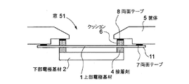
携帯電話機などの携帯端末に用いられる抵抗膜式タッチパネルの構造は、図5に示す如く、2枚の上部及び下部の電極基材1,2を、所定間隙をもって対抗するように両面テープなどの接着材4により接着して構成されている。上部電極基材(以下、上部基材と称する)1としては、一般的には、PETフィルムが用いられており、下部電極基材(以下、下部基材と称する)2としては、一般的には、ガラスが用いられている。
As shown in FIG. 5, the structure of a resistive touch panel used for a portable terminal such as a cellular phone is such that two upper and
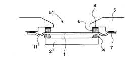
上部基材1の外周には、電極引き回しエリア3が設けられており、その一部から電極引き出し部9が導出されている。このように構成されたタッチパネルは、図6に示す如く、装置筐体5に設けられた窓51にクッション6を介して取付けられる。
An electrode routing area 3 is provided on the outer periphery of the
ここで、上部基材1はPETなどのフィルムで作られており、温度や温度による膨張や収縮があり、またガラスで作られることが多い下部基材2との熱膨張係数の相違があり、よって、図7に示す如く、両基材1と2とを接着する接着材4としては、横方向のずれに対する強度が低いものを用いて、横方向のずれを吸収するようになっている。
Here, the
そのために、従来の抵抗膜式タッチパネルの装置筐体5への組み込み方法は、図6に示しているように、筐体5とクッション6との間を、両面テープ8で接着し、クッション6と上部基材1の電極引き回しエリア3との間は接着せずに、筐体5へ押しつけるように取付けるか、筐体5とクッション6との間は接着せずに、クッション6と上部基材1の電極引き回しエリア3との間を接着して、筐体5へ押し付けるようになっている。よって、接着していない隙間から、塵埃や水滴が侵入し易くなる。
For this purpose, as shown in FIG. 6, the conventional method of assembling the resistive touch panel in the
ここで、特許文献1を参照すると、タッチパネルの構造において、充分な防塵や防水機能を施した技術が提案されている。
上述した図5、図6の構造においては、塵埃や水滴の侵入を防ぐことができないという問題があり、防塵や防水効果を向上させるために、上述した隙間を接着剤10(両面テープ)で接着してしまうと、温度や湿度により、上部基材1の膨張や収縮が発生し、図8に示す如く、タッチパネル面がシワになってしまい、外観上問題がある。また、特許文献1の技術でも、両基材の熱膨張係数の違いによる膨張や収縮については、何等考慮されておらず、やはり問題がある。
In the structure of FIG. 5 and FIG. 6 described above, there is a problem that intrusion of dust and water droplets cannot be prevented. If it does, expansion | swelling and shrinkage | contraction of the
本発明の目的は、防塵や防水効果を高めると同時に、外観上のシワの問題をも解決可能としたパネル構造及びその取り付け構造を提供することである。 It is an object of the present invention to provide a panel structure and its mounting structure that can improve the dustproof and waterproof effect and at the same time solve the problem of wrinkles on the appearance.
本発明によるパネル構造は、熱膨張が異なる上部及び下部基材を、所定間隙をもって対向するように接着剤により接着して構成され、装置筐体に設けられた窓に取り付けるためのパネル構造であって、前記接着材は前記基材の熱膨張差によるずれを吸収可能であり、前記上部基材は前記下部基材の面積よりも大とされ、かつその外周部分において面方向の変形力が吸収自在な構成であることを特徴とする。 The panel structure according to the present invention is a panel structure in which upper and lower substrates having different thermal expansions are bonded with an adhesive so as to face each other with a predetermined gap, and are attached to a window provided in the apparatus housing. The adhesive can absorb the deviation due to the difference in thermal expansion of the base material, the upper base material is made larger than the area of the lower base material, and the deformation force in the surface direction is absorbed in the outer peripheral portion thereof. It is a free configuration.
本発明によるパネル取り付け構造は、上述のパネル構造を前記基材より小なる筐体窓に取り付けるパネル取り付け構造であって、前記上部基材の最外周全体を前記筐体に接着してなることを特徴とする。 The panel mounting structure according to the present invention is a panel mounting structure in which the above-described panel structure is mounted on a housing window smaller than the base material, and the entire outermost periphery of the upper base material is bonded to the housing. Features.
本発明の作用を述べる。熱膨張が異なる上部及び下部基材を、所定間隙をもって対向するように接着剤により接着して構成され、装置筐体に設けられた窓に取り付けるためのパネル構造において、当該接着材によって上部及び下部基材間の熱膨張差によるずれを吸収可能とし、上部基材は下部基材の面積よりも大とし、かつその外周部分において面方向の変形力が吸収自在な構成とする。これにより、筐体との隙間を完全に密閉しても、両基材間の熱膨張差による面方向のずれが吸収でき、防塵及び防水効果が図れる。 The operation of the present invention will be described. In the panel structure for attaching the upper and lower base materials having different thermal expansion to each other with an adhesive so as to face each other with a predetermined gap, and attaching to the window provided in the apparatus housing, The shift due to the difference in thermal expansion between the substrates can be absorbed, the upper substrate is made larger than the area of the lower substrate, and the deformation force in the plane direction can be absorbed at the outer peripheral portion. Thereby, even if the gap with the housing is completely sealed, the deviation in the surface direction due to the difference in thermal expansion between both base materials can be absorbed, and a dustproof and waterproof effect can be achieved.
本発明によれば、上部及び下部基材間の熱膨張差によるずれを吸収可能とし、上部基材は下部基材の面積よりも大とし、かつその外周部分において面方向の変形力が吸収自在な構成としたので、上部基材のしわがなくなり、かつ筐体との間の密閉が、上部基材の外周部で可能になり、よって、防塵及び防水機能が果たせるという効果がある。 According to the present invention, it is possible to absorb the deviation due to the difference in thermal expansion between the upper and lower substrates, the upper substrate is larger than the area of the lower substrate, and the deformation force in the plane direction can be absorbed at the outer peripheral portion thereof. Since the upper base material is configured, the upper base material is free from wrinkles and can be sealed with the casing at the outer peripheral portion of the upper base material. Therefore, there is an effect that a dustproof and waterproof function can be achieved.
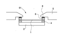
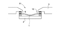
以下に、図面を用いて本発明の実施の形態について説明する。図1は本発明の一実施の形態を示す断面図であり図5〜図8と同等部分は同一符号により示している。図1を参照すると、上部基板1と下部基材2とは、接着材4により所定間隙をもって対向配置されており、この接着材4は、図7に示したように、両基材の熱膨張差に起因する面方向のずれを吸収自在な両面テープなどが用いられる。
Embodiments of the present invention will be described below with reference to the drawings. FIG. 1 is a cross-sectional view showing an embodiment of the present invention, and the same parts as those in FIGS. Referring to FIG. 1, the
上部基材1の面積は下部基材2のそれよりも大とされており、下部基材2よりも突出した外周部分11の最外周全体にわたって、装置筐体5に接着用両面テープ7により、取り付けられている。筐体5の窓51の周囲に対しては、クッション6により、上部基材1の電極引き回しエリア3(図5参照)部分が押し付けられており、クッション6と上部基材1とは接着されておらず、クッション6と窓51の周囲とが両面テープ8により接着されている。
The area of the
図2に示す如く、温度や温度により、上部基材1が面方向にひずむと、接着材4の面方向の変形の吸収作用により、窓51に相当する上部基材1の部分のひずみは吸収され、しわが生ずることはないが、上部基材1の外周部分11において、しわを逃がすことができる。従って、図3に示す如く、外周部分を予めジャバラ状12に屈曲して成形しておき、膨張収縮の吸収効果をより一層向上させるようにしても良く、また外周部分を、他部分より薄くするようにしても、上記の吸収効果は向上する。
As shown in FIG. 2, when the
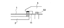
図4は筐体5と上部基材1との取り付け方法の他の例を示す断面図であり、接着材としての両面テープを用いる代りに筐体5に予め設けられている凹溝部52に、上部基材1の外周部分11の最外周全体を嵌め込むことにより、筐体5への取付けを、隙間なく完全に行うことができる。
FIG. 4 is a cross-sectional view showing another example of a method for attaching the
上記の実施の形態においては、携帯電話機などの携帯情報端末のタッチパネルに用いる場合について説明したが、一般に熱膨張が異なる2枚の上部及び下部基材を接着材により所定間隙をもって対向配置したパネル構造に広く適用できるものである。 In the above embodiment, the case where it is used for a touch panel of a portable information terminal such as a cellular phone has been described. Generally, a panel structure in which two upper and lower substrates having different thermal expansion are arranged opposite to each other with a predetermined gap by an adhesive. It can be widely applied to.
1 上部電極基材
2 下部電極基材
3 電極引き回しエリア
4 接着材
5 筐体
6 クッション
7,8 両面テープ
11 外周部
12 屈曲部
51 筐体窓
52 凹部溝
DESCRIPTION OF
Claims (7)
The panel mounting structure according to claim 5 or 6, wherein the panel mounting structure is used for a touch panel of a portable terminal.
Priority Applications (1)
| Application Number | Priority Date | Filing Date | Title |
|---|---|---|---|
| JP2004048862A JP2005242501A (en) | 2004-02-25 | 2004-02-25 | Panel structure and its mounting structure |
Applications Claiming Priority (1)
| Application Number | Priority Date | Filing Date | Title |
|---|---|---|---|
| JP2004048862A JP2005242501A (en) | 2004-02-25 | 2004-02-25 | Panel structure and its mounting structure |
Publications (1)
| Publication Number | Publication Date |
|---|---|
| JP2005242501A true JP2005242501A (en) | 2005-09-08 |
Family
ID=35024205
Family Applications (1)
| Application Number | Title | Priority Date | Filing Date |
|---|---|---|---|
| JP2004048862A Pending JP2005242501A (en) | 2004-02-25 | 2004-02-25 | Panel structure and its mounting structure |
Country Status (1)
| Country | Link |
|---|---|
| JP (1) | JP2005242501A (en) |
Cited By (10)
| Publication number | Priority date | Publication date | Assignee | Title |
|---|---|---|---|---|
| JP2007316861A (en) * | 2006-05-24 | 2007-12-06 | Sharp Corp | Sealing structure |
| WO2010064545A1 (en) | 2008-12-01 | 2010-06-10 | 株式会社 翔栄 | Input device utilizing touch panel |
| US8044938B2 (en) | 2006-07-07 | 2011-10-25 | Alps Electric Co., Ltd. | Input device with improved touch panel surface and electronic device having the input device |
| WO2012096113A1 (en) * | 2011-01-15 | 2012-07-19 | 京セラ株式会社 | Electronic apparatus and mobile terminal provided therewith |
| DE102011011982A1 (en) * | 2011-02-22 | 2012-08-23 | Bizerba Gmbh & Co Kg | Operating device for a product processing device |
| WO2012114768A1 (en) * | 2011-02-24 | 2012-08-30 | 京セラ株式会社 | Electronic device |
| WO2012140877A1 (en) * | 2011-04-11 | 2012-10-18 | 京セラ株式会社 | Electronic device |
| JP2012216205A (en) * | 2011-04-01 | 2012-11-08 | Kyocera Corp | Electronic device |
| JP2013114463A (en) * | 2011-11-29 | 2013-06-10 | Denso Corp | Operation device |
| JP2014127071A (en) * | 2012-12-27 | 2014-07-07 | Fujitsu Component Ltd | Touch input device |
-
2004
- 2004-02-25 JP JP2004048862A patent/JP2005242501A/en active Pending
Cited By (17)
| Publication number | Priority date | Publication date | Assignee | Title |
|---|---|---|---|---|
| JP2007316861A (en) * | 2006-05-24 | 2007-12-06 | Sharp Corp | Sealing structure |
| JP4619990B2 (en) * | 2006-05-24 | 2011-01-26 | シャープ株式会社 | Seal structure |
| CN101504581B (en) * | 2006-07-07 | 2011-12-21 | 阿尔卑斯电气株式会社 | Input device |
| US8044938B2 (en) | 2006-07-07 | 2011-10-25 | Alps Electric Co., Ltd. | Input device with improved touch panel surface and electronic device having the input device |
| US8525812B2 (en) | 2008-12-01 | 2013-09-03 | Shoei Co., Ltd. | Input device using touch panel |
| WO2010064545A1 (en) | 2008-12-01 | 2010-06-10 | 株式会社 翔栄 | Input device utilizing touch panel |
| WO2012096113A1 (en) * | 2011-01-15 | 2012-07-19 | 京セラ株式会社 | Electronic apparatus and mobile terminal provided therewith |
| JP5116902B2 (en) * | 2011-01-15 | 2013-01-09 | 京セラ株式会社 | Electronic device and portable terminal equipped with the same |
| US9060438B2 (en) | 2011-01-15 | 2015-06-16 | Kyocera Corporation | Electronic device and mobile terminal including the same |
| DE102011011982A1 (en) * | 2011-02-22 | 2012-08-23 | Bizerba Gmbh & Co Kg | Operating device for a product processing device |
| EP2492790A3 (en) * | 2011-02-22 | 2018-01-24 | Bizerba SE & Co. KG | Operating device for a product processing device |
| WO2012114768A1 (en) * | 2011-02-24 | 2012-08-30 | 京セラ株式会社 | Electronic device |
| JP5530026B2 (en) * | 2011-02-24 | 2014-06-25 | 京セラ株式会社 | Electronics |
| JP2012216205A (en) * | 2011-04-01 | 2012-11-08 | Kyocera Corp | Electronic device |
| WO2012140877A1 (en) * | 2011-04-11 | 2012-10-18 | 京セラ株式会社 | Electronic device |
| JP2013114463A (en) * | 2011-11-29 | 2013-06-10 | Denso Corp | Operation device |
| JP2014127071A (en) * | 2012-12-27 | 2014-07-07 | Fujitsu Component Ltd | Touch input device |
Similar Documents
| Publication | Publication Date | Title |
|---|---|---|
| JP5134327B2 (en) | Display device | |
| JP4833201B2 (en) | Stress sealing for touch screen systems | |
| JP2004046835A (en) | Lcd assembly for radio information terminal apparatus | |
| JP2010537240A (en) | Dust sealing tape, display using dust sealing tape, and sealing method | |
| JP2007256518A (en) | Liquid crystal display device | |
| JP2005242501A (en) | Panel structure and its mounting structure | |
| JP4267554B2 (en) | Display structure of electronic device and electronic device provided with the same | |
| JP5034628B2 (en) | Portable information equipment | |
| JP2008097012A (en) | Display panel module | |
| JP2019526062A (en) | Display module, display device having display module, and method of manufacturing display module | |
| CN113471258B (en) | Display device | |
| JP4299737B2 (en) | Display device and electronic apparatus using the display device | |
| JP2005077349A5 (en) | ||
| JP2008233217A (en) | Display device | |
| JP2016536196A (en) | Wind shield and sealing element | |
| WO2010073298A1 (en) | Panel structure and casing for electronic device | |
| JP4985552B2 (en) | Waterproof window structure and electronic equipment | |
| JP2016009371A (en) | Touch panel, fixing structure of front face design sheet, and display device with touch panel | |
| JP2004186171A (en) | Fixing structure of display section and portable terminal employing it | |
| JP5054501B2 (en) | Gas meter ventilation structure and affixed filter | |
| JP4066641B2 (en) | Touch panel | |
| JP4990225B2 (en) | Liquid crystal display | |
| JP2008111297A (en) | Setting block and sash using it | |
| US20140184981A1 (en) | Display apparatus | |
| JP2000047820A (en) | Transparent touch panel and display device using the panel |
Legal Events
| Date | Code | Title | Description |
|---|---|---|---|
| A621 | Written request for application examination |
Free format text: JAPANESE INTERMEDIATE CODE: A621 Effective date: 20070115 |
|
| A977 | Report on retrieval |
Free format text: JAPANESE INTERMEDIATE CODE: A971007 Effective date: 20090105 |
|
| A131 | Notification of reasons for refusal |
Free format text: JAPANESE INTERMEDIATE CODE: A131 Effective date: 20090324 |
|
| A521 | Request for written amendment filed |
Free format text: JAPANESE INTERMEDIATE CODE: A523 Effective date: 20090525 |
|
| A02 | Decision of refusal |
Free format text: JAPANESE INTERMEDIATE CODE: A02 Effective date: 20090714 |