JP4732991B2 - El装置 - Google Patents
El装置 Download PDFInfo
- Publication number
- JP4732991B2 JP4732991B2 JP2006260485A JP2006260485A JP4732991B2 JP 4732991 B2 JP4732991 B2 JP 4732991B2 JP 2006260485 A JP2006260485 A JP 2006260485A JP 2006260485 A JP2006260485 A JP 2006260485A JP 4732991 B2 JP4732991 B2 JP 4732991B2
- Authority
- JP
- Japan
- Prior art keywords
- light
- emitting layer
- light output
- color
- emission
- Prior art date
- Legal status (The legal status is an assumption and is not a legal conclusion. Google has not performed a legal analysis and makes no representation as to the accuracy of the status listed.)
- Active
Links
Images


Classifications
-
- H—ELECTRICITY
- H10—SEMICONDUCTOR DEVICES; ELECTRIC SOLID-STATE DEVICES NOT OTHERWISE PROVIDED FOR
- H10K—ORGANIC ELECTRIC SOLID-STATE DEVICES
- H10K50/00—Organic light-emitting devices
- H10K50/80—Constructional details
- H10K50/85—Arrangements for extracting light from the devices
- H10K50/852—Arrangements for extracting light from the devices comprising a resonant cavity structure, e.g. Bragg reflector pair
Landscapes
- Physics & Mathematics (AREA)
- Optics & Photonics (AREA)
- Electroluminescent Light Sources (AREA)
- Devices For Indicating Variable Information By Combining Individual Elements (AREA)
Description
する。
<色ずれの発生原理>
本実施形態の構成について説明する前に、まず色ずれの発生原理について説明する。
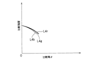
具体的には、出射角θ=0°からθが大きくなるのに伴って、赤色の光の出射強度の比率は増大するが、緑色及び青色の光の出射強度の比率は小さくなる。このため、正面方向D2を基準に白色光を出力していても、斜め方向からEL装置を見ると、赤色の成分の比率が相対的に上がっている分、赤みがかって見えるようになっている。
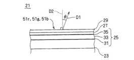
図9は、本発明の第1実施形態に係るEL装置の構成を概略的に示す断面図である。このEL装置21は、トップエミッションタイプであり、図9に示すように、透明基板であるガラス基板23と、そのガラス基板23上に形成された素子部25と、その素子部25の上に形成された調整層27と、その調整層27の上から素子部25全体を覆うように形成された封止膜29とを備えている。素子部25は、基板23側から順に、第1の電極31、有機層33及び第2の電極35を備えている。有機層33が第1及び第2の電極31,35によって挟み込まれている。
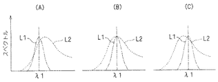
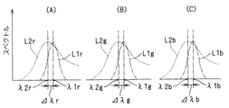
上述の色ずれの問題に対する本実施形態に係るEL装置21の構成について説明する。図11(A)ないし図11(C)は、本実施形態に係るEL装置における第1ないし第3の光出力部の発光スペクトルと透過スペクトルとの関係を例示的に示す図である。
以下に、従来のEL装置に対応する比較例と、本実施形態に係るEL装置21の具体的な実施例とを比較して説明する。なお、この実施例では、電極31,35間の共振器構造要素に主に着目し、比較例との比較を行っている。
(b) 正孔輸送層43
材料:NPB
膜厚:70nm(赤)、50nm(緑、青)
(c) 発光層45
ホスト材料:Alq3(赤、緑)、SDPVBi(青)
ホスト膜厚:60nm(赤)、50nm(緑)、20nm(青)
ドーパント材料:DCJTB(赤)、クマリン(緑)、スチリルアミン(青)
(d) 電子輸送層47:無し
(e) 電子注入層49
材料:マグネシウム
膜厚:10nm
(f) 第2の電極(陰極)35
材料:ITO
膜厚:100nm
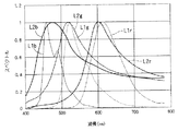
図13は、比較例の構成に基づいて各色の発光スペクトルと正面方向を基準とした透過スペクトルとの関係について行った光学シミュレーション結果を示す図である。図13が示すシミュレーション結果より、赤色の透過スペクトル(L2r)の共振ピーク波長は赤色の発光スペクトル(L1r)の発光ピーク波長の短波長側にあり、緑色の透過スペクトル(L2g)の共振ピーク波長は緑色の発光スペクトル(L1g)の発光ピーク波長とほぼ一致しており、青色の透過スペクトル(L2b)の共振ピーク波長は青色の発光スペクトル(L1b)の発光ピーク波長の長波長側にあることが分かる。
(b) 正孔輸送層43
材料:NPB
膜厚:70nm(赤)、50nm(緑、青)
(c) 発光層45
ホスト材料:Alq3(赤、緑)、SDPVBi(青)
ホスト膜厚:68nm(赤)、65nm(緑)、20nm(青)
ドーパント材料:DCJTB(赤)、クマリン(緑)、スチリルアミン(青)
(d) 電子輸送層47:無し
(e) 電子注入層49
材料:マグネシウム
膜厚:10nm
(f) 第2の電極(陰極)35
材料:ITO
膜厚:100nm
図15は、上記の実施例の構成に基づいて各色の発光スペクトルと正面方向を基準とした透過スペクトルとの関係について行った光学シミュレーション結果を示す図である。図15が示すシミュレーション結果より、赤、緑、青のすべての色の透過スペクトル(L2r,L2g,L2b)の共振ピーク波長が、対応する色の発光スペクトル(L1r,L1g,L1b)の発光ピーク波長の長波長側に設定されている。
本実施形態に係るEL装置21が上述の第1実施形態に係るEL装置21と実質的に異なる点は、第1ないし第3の各光出力部51r,51g,51bにおける発光スペクトルに対する透過スペクトルの設定条件が異なるのみであり、大まかな装置構成は互いに共通しており、重複する部分については同一の参照符号を用い、説明を省略する。
図19は、本発明の第3実施形態に係るEL装置の構成を概略的に示す断面図である。なお、図19の構成において、上記の図9の構成とおおよそ対応する部分には同一の参照符号を付し、説明の重複を回避することとする。
3 有機層
5,7 反射面
9 共振器構造
10 光出力部
21 EL装置
23 ガラス基板
25 素子部
27 調整層
29 封止膜
31 第1の電極
33 有機層
35 第2の電極
41 電荷注入層
43 電荷輸送層
45 発光層
47 電荷輸送層
49 電荷注入層
51r 第1の光出力部
51g 第2の光出力部
51b 第3の光出力部
61 EL装置
D1 出射方向
D2 正面方向
θ 出射角
Claims (8)
- EL装置において、
発光層と、該発光層の発する光を共振する共振器構造と、を備えた複数の光出力部を有し、
前記複数の光出力部は、第1の色の光を発する発光層を有する第1の光出力部と、前記第1の色と異なる色の光を発する発光層を有する第2の光出力部と、前記第1及び第2の光と異なる色の光を発する発光層を有する第3の光出力部と、を含んで構成され、
前記第1乃至第3の光出力部に関して、前記発光層の主面に対して直交する方向に前記共振器構造を透過した光の透過スペクトルのピーク値を示す共振ピーク波長が、前記発光層が発光する光の発光スペクトルのピーク値を示す発光ピーク波長よりも長波長側にあるとともに、
前記第1乃至第3の光出力部の発する光の前記発光ピーク波長とそれに対応する前記各共振ピーク波長との差をそれぞれΔλr、Δλg、Δλbとしたとき、0.5≦Δλg/Δλr≦2、及び0.5≦Δλb/Δλg≦2となることを特徴とするEL装置。 - 請求項1に記載のEL装置において、
前記第1乃至第3の光出力部の共振ピーク波長は、可視光領域に存在することを特徴とするEL装置。 - 請求項1に記載のEL装置において、
前記第1の色は赤色、前記第2の色は緑色、前記第3の色は青色であることを特徴とするEL装置。 - 請求項1に記載のEL装置において、
前記第1乃至第3の光出力部の前記共振器構造は、
前記発光層の厚み方向の両側に設けられる一対の2つの電極の間に形成される単数もしくは複数の層を含むことを特徴とするEL装置。 - EL装置において、
発光層と、該発光層の発する光を共振する共振器構造と、を備えた複数の光出力部を有し、
前記複数の光出力部は、第1の色の光を発する発光層を有する第1の光出力部と、前記第1の色と異なる色の光を発する発光層を有する第2の光出力部と、前記第1及び第2の光と異なる色の光を発する発光層を有する第3の光出力部と、を含んで構成され、
前記第1乃至第3の光出力部に関して、前記発光層の主面に対して直交する方向に前記共振器構造を透過した光の透過スペクトルのピーク値を示す共振ピーク波長が、前記発光層が発光する光の発光スペクトルのピーク値を示す発光ピーク波長よりも長波長側にあるとともに、
前記第1乃至第3の光出力部を搭載する基板と、前記第1乃至第3の光出力部を被覆し、前記第1乃至第3の光出力部が発する光を透過する封止膜と、を更に備え、
前記各光出力部の前記共振器構造は封止膜を含むことを特徴とするEL装置。 - EL装置において、
発光層と、該発光層の発する光を共振する共振器構造と、を備えた複数の光出力部を有し、
前記複数の光出力部は、第1の色の光を発する発光層を有する第1の光出力部と、前記第1の色と異なる色の光を発する発光層を有する第2の光出力部と、前記第1及び第2の光と異なる色の光を発する発光層を有する第3の光出力部と、を含んで構成され、
前記第1乃至第3の光出力部に関して、前記発光層の主面に対して直交する方向に前記共振器構造を透過した光の透過スペクトルのピーク値を示す共振ピーク波長が、前記発光層が発光する光の発光スペクトルのピーク値を示す発光ピーク波長よりも長波長側にあるとともに、
前記第1乃至第3の光出力部を搭載し、前記第1乃至第3の光出力部が発する光を透過する透明基板を更に備え、
前記各光出力部の前記共振器構造は、前記透明基板を含むことを特徴とするEL装置。 - EL装置において、
発光層と、該発光層の発する光を共振する共振器構造と、を備えた複数の光出力部を有し、
前記複数の光出力部は、第1の色の光を発する発光層を有する第1の光出力部と、前記第1の色と異なる色の光を発する発光層を有する第2の光出力部と、前記第1及び第2の光と異なる色の光を発する発光層を有する第3の光出力部と、を含んで構成され、
前記第1乃至第3の光出力部に関して、前記発光層の主面に対して直交する方向に前記共振器構造を透過した光の透過スペクトルのピーク値を示す共振ピーク波長が、前記発光層が発光する光の発光スペクトルのピーク値を示す発光ピーク波長よりも長波長側にあるとともに、
前記第1乃至第3の光出力部の前記共振器構造は、
前記第1乃至第3の光出力部の発する光が外部に向けて出射されるまでに通過する全ての層および部材を含むことを特徴とするEL装置。 - EL装置において、
発光層と、該発光層の発する光を共振する共振器構造と、を備えた複数の光出力部を有し、
前記複数の光出力部は、第1の色の光を発する発光層を有する第1の光出力部と、前記第1の色と異なる色の光を発する発光層を有する第2の光出力部と、前記第1及び第2の光と異なる色の光を発する発光層を有する第3の光出力部と、を含んで構成され、
前記第1乃至第3の光出力部に関して、前記発光層の主面に対して直交する方向に前記共振器構造を透過した光の透過スペクトルのピーク値を示す共振ピーク波長が、前記発光層が発光する光の発光スペクトルのピーク値を示す発光ピーク波長よりも長波長側にあるとともに、
前記第1乃至第3の光出力部の発する光の前記発光ピーク波長とそれに対応する前記各共振ピーク波長との差の絶対値は、前記共振器構造の厚みが大きい光出力部ほど大きく設定されていることを特徴とするEL装置。
Priority Applications (1)
| Application Number | Priority Date | Filing Date | Title |
|---|---|---|---|
| JP2006260485A JP4732991B2 (ja) | 2005-09-26 | 2006-09-26 | El装置 |
Applications Claiming Priority (3)
| Application Number | Priority Date | Filing Date | Title |
|---|---|---|---|
| JP2005278157 | 2005-09-26 | ||
| JP2005278157 | 2005-09-26 | ||
| JP2006260485A JP4732991B2 (ja) | 2005-09-26 | 2006-09-26 | El装置 |
Related Child Applications (1)
| Application Number | Title | Priority Date | Filing Date |
|---|---|---|---|
| JP2011077791A Division JP5073842B2 (ja) | 2005-09-26 | 2011-03-31 | El装置 |
Publications (2)
| Publication Number | Publication Date |
|---|---|
| JP2007115679A JP2007115679A (ja) | 2007-05-10 |
| JP4732991B2 true JP4732991B2 (ja) | 2011-07-27 |
Family
ID=38097653
Family Applications (1)
| Application Number | Title | Priority Date | Filing Date |
|---|---|---|---|
| JP2006260485A Active JP4732991B2 (ja) | 2005-09-26 | 2006-09-26 | El装置 |
Country Status (1)
| Country | Link |
|---|---|
| JP (1) | JP4732991B2 (ja) |
Families Citing this family (13)
| Publication number | Priority date | Publication date | Assignee | Title |
|---|---|---|---|---|
| JP4588603B2 (ja) * | 2005-09-30 | 2010-12-01 | 京セラ株式会社 | 電界発光装置 |
| JP2009170127A (ja) * | 2008-01-11 | 2009-07-30 | Seiko Epson Corp | 発光装置及び電子機器 |
| WO2010143231A1 (ja) * | 2009-06-11 | 2010-12-16 | パイオニア株式会社 | 発光素子及び表示装置 |
| CN102804921B (zh) * | 2009-06-11 | 2016-05-25 | 日本先锋公司 | 发光元件和显示装置 |
| JP2011210677A (ja) * | 2010-03-30 | 2011-10-20 | Fujifilm Corp | 有機電界発光装置 |
| JP2011210678A (ja) * | 2010-03-30 | 2011-10-20 | Fujifilm Corp | 有機電界発光装置 |
| JP5760699B2 (ja) * | 2011-05-27 | 2015-08-12 | セイコーエプソン株式会社 | 発光装置および電子機器 |
| JP5485966B2 (ja) * | 2011-10-25 | 2014-05-07 | パイオニア株式会社 | 発光素子 |
| JP6111478B2 (ja) * | 2012-07-04 | 2017-04-12 | 株式会社Joled | 発光素子及び表示装置 |
| US10529780B2 (en) * | 2017-02-28 | 2020-01-07 | Semiconductor Energy Laboratory Co., Ltd. | Display device, display module, and electronic device |
| JP7176552B2 (ja) | 2020-08-31 | 2022-11-22 | セイコーエプソン株式会社 | 電気光学装置および電子機器 |
| JP7753128B2 (ja) | 2021-04-13 | 2025-10-14 | キヤノン株式会社 | 発光装置、表示装置、光電変換装置、電子機器、照明装置、および移動体 |
| JP7703467B2 (ja) * | 2021-04-13 | 2025-07-07 | キヤノン株式会社 | 発光装置、表示装置、撮像装置、及び、電子機器 |
Family Cites Families (5)
| Publication number | Priority date | Publication date | Assignee | Title |
|---|---|---|---|---|
| JPH1167448A (ja) * | 1997-08-26 | 1999-03-09 | Toyota Central Res & Dev Lab Inc | ディスプレイ装置 |
| JP2001071558A (ja) * | 1999-09-03 | 2001-03-21 | Futaba Corp | Elプリンタ及びel素子 |
| EP2169738A3 (en) * | 1999-11-22 | 2012-11-07 | Sony Corporation | Display device |
| JP3508741B2 (ja) * | 2001-06-05 | 2004-03-22 | ソニー株式会社 | 表示素子 |
| JP2007052971A (ja) * | 2005-08-17 | 2007-03-01 | Seiko Epson Corp | 発光装置、その設計方法および電子機器 |
-
2006
- 2006-09-26 JP JP2006260485A patent/JP4732991B2/ja active Active
Also Published As
| Publication number | Publication date |
|---|---|
| JP2007115679A (ja) | 2007-05-10 |
Similar Documents
| Publication | Publication Date | Title |
|---|---|---|
| JP5073842B2 (ja) | El装置 | |
| US8593056B2 (en) | Electroluminescent device | |
| KR101434361B1 (ko) | 백색 유기 전계 발광소자 및 이를 이용한 컬러 디스플레이장치 | |
| US7102282B1 (en) | Display device with a cavity structure for resonating light | |
| CN101409330B (zh) | 白光有机发光器件及采用其的彩色显示设备 | |
| JP7495401B2 (ja) | 複数個の青色放射層を有するマルチモーダルマイクロキャビティoled | |
| US20090096358A1 (en) | White organic light emitting device and color display apparatus employing the same | |
| JP4732991B2 (ja) | El装置 | |
| TWI699022B (zh) | 發光裝置、顯示設備以及照明設備 | |
| JP4817789B2 (ja) | 有機el表示装置 | |
| JP2020043059A (ja) | 有機発光ダイオードマイクロスクリーン用のピクセル | |
| JP2005276662A (ja) | 発光表示装置 | |
| WO2016031757A1 (ja) | 有機エレクトロルミネッセンス装置、有機エレクトロルミネッセンス装置の製造方法、照明装置、および表示装置 | |
| JP4655959B2 (ja) | 表示素子 | |
| JP5309388B2 (ja) | 自発光素子および表示装置 | |
| JP4548404B2 (ja) | 表示装置 | |
| US7545096B2 (en) | Trans-reflective organic electroluminescent panel and method of fabricating the same | |
| JPH053081A (ja) | 面発光装置 | |
| JP7317614B2 (ja) | 表示装置 | |
| JP2013157276A (ja) | 発光装置、画像形成装置及び撮像装置 | |
| JP2011141965A (ja) | 有機el素子および表示装置 |
Legal Events
| Date | Code | Title | Description |
|---|---|---|---|
| A621 | Written request for application examination |
Free format text: JAPANESE INTERMEDIATE CODE: A621 Effective date: 20090316 |
|
| RD04 | Notification of resignation of power of attorney |
Free format text: JAPANESE INTERMEDIATE CODE: A7424 Effective date: 20090615 |
|
| A977 | Report on retrieval |
Free format text: JAPANESE INTERMEDIATE CODE: A971007 Effective date: 20110208 |
|
| A131 | Notification of reasons for refusal |
Free format text: JAPANESE INTERMEDIATE CODE: A131 Effective date: 20110215 |
|
| A521 | Request for written amendment filed |
Free format text: JAPANESE INTERMEDIATE CODE: A523 Effective date: 20110331 |
|
| TRDD | Decision of grant or rejection written | ||
| A01 | Written decision to grant a patent or to grant a registration (utility model) |
Free format text: JAPANESE INTERMEDIATE CODE: A01 Effective date: 20110419 |
|
| A01 | Written decision to grant a patent or to grant a registration (utility model) |
Free format text: JAPANESE INTERMEDIATE CODE: A01 |
|
| A61 | First payment of annual fees (during grant procedure) |
Free format text: JAPANESE INTERMEDIATE CODE: A61 Effective date: 20110421 |
|
| FPAY | Renewal fee payment (event date is renewal date of database) |
Free format text: PAYMENT UNTIL: 20140428 Year of fee payment: 3 |
|
| R150 | Certificate of patent or registration of utility model |
Ref document number: 4732991 Country of ref document: JP Free format text: JAPANESE INTERMEDIATE CODE: R150 Free format text: JAPANESE INTERMEDIATE CODE: R150 |
|
| S111 | Request for change of ownership or part of ownership |
Free format text: JAPANESE INTERMEDIATE CODE: R313113 |
|
| FPAY | Renewal fee payment (event date is renewal date of database) |
Free format text: PAYMENT UNTIL: 20140428 Year of fee payment: 3 |
|
| R350 | Written notification of registration of transfer |
Free format text: JAPANESE INTERMEDIATE CODE: R350 |
|
| R250 | Receipt of annual fees |
Free format text: JAPANESE INTERMEDIATE CODE: R250 |
|
| R250 | Receipt of annual fees |
Free format text: JAPANESE INTERMEDIATE CODE: R250 |
|
| R250 | Receipt of annual fees |
Free format text: JAPANESE INTERMEDIATE CODE: R250 |
|
| R250 | Receipt of annual fees |
Free format text: JAPANESE INTERMEDIATE CODE: R250 |
|
| R250 | Receipt of annual fees |
Free format text: JAPANESE INTERMEDIATE CODE: R250 |
|
| R250 | Receipt of annual fees |
Free format text: JAPANESE INTERMEDIATE CODE: R250 |
|
| R250 | Receipt of annual fees |
Free format text: JAPANESE INTERMEDIATE CODE: R250 |
|
| R250 | Receipt of annual fees |
Free format text: JAPANESE INTERMEDIATE CODE: R250 |
|
| R250 | Receipt of annual fees |
Free format text: JAPANESE INTERMEDIATE CODE: R250 |
|
| R250 | Receipt of annual fees |
Free format text: JAPANESE INTERMEDIATE CODE: R250 |
|
| R250 | Receipt of annual fees |
Free format text: JAPANESE INTERMEDIATE CODE: R250 |
|
| R250 | Receipt of annual fees |
Free format text: JAPANESE INTERMEDIATE CODE: R250 |