JP4732685B2 - Equipment for coating articles - Google Patents
Equipment for coating articles Download PDFInfo
- Publication number
- JP4732685B2 JP4732685B2 JP2003519960A JP2003519960A JP4732685B2 JP 4732685 B2 JP4732685 B2 JP 4732685B2 JP 2003519960 A JP2003519960 A JP 2003519960A JP 2003519960 A JP2003519960 A JP 2003519960A JP 4732685 B2 JP4732685 B2 JP 4732685B2
- Authority
- JP
- Japan
- Prior art keywords
- coating
- conductor
- rim
- waveguide
- chambers
- Prior art date
- Legal status (The legal status is an assumption and is not a legal conclusion. Google has not performed a legal analysis and makes no representation as to the accuracy of the status listed.)
- Expired - Lifetime
Links
- 238000000576 coating method Methods 0.000 title claims abstract description 87
- 239000011248 coating agent Substances 0.000 title claims abstract description 85
- 239000004020 conductor Substances 0.000 claims description 85
- 229910052751 metal Inorganic materials 0.000 claims description 9
- 239000002184 metal Substances 0.000 claims description 9
- 239000000758 substrate Substances 0.000 claims description 6
- 230000005670 electromagnetic radiation Effects 0.000 claims description 2
- 238000001514 detection method Methods 0.000 claims 1
- 230000005855 radiation Effects 0.000 claims 1
- 238000011144 upstream manufacturing Methods 0.000 claims 1
- 210000002381 plasma Anatomy 0.000 abstract 1
- 230000008859 change Effects 0.000 description 5
- 238000010586 diagram Methods 0.000 description 5
- 238000000034 method Methods 0.000 description 4
- 239000000203 mixture Substances 0.000 description 4
- 239000003708 ampul Substances 0.000 description 3
- 230000006837 decompression Effects 0.000 description 3
- 230000005672 electromagnetic field Effects 0.000 description 3
- 238000004519 manufacturing process Methods 0.000 description 3
- 230000008569 process Effects 0.000 description 3
- 238000006073 displacement reaction Methods 0.000 description 2
- 238000005265 energy consumption Methods 0.000 description 2
- 239000011521 glass Substances 0.000 description 2
- 239000011810 insulating material Substances 0.000 description 2
- 238000010884 ion-beam technique Methods 0.000 description 2
- 230000008901 benefit Effects 0.000 description 1
- 238000005229 chemical vapour deposition Methods 0.000 description 1
- 230000001419 dependent effect Effects 0.000 description 1
- 230000000694 effects Effects 0.000 description 1
- 238000005516 engineering process Methods 0.000 description 1
- 230000005284 excitation Effects 0.000 description 1
- UQEAIHBTYFGYIE-UHFFFAOYSA-N hexamethyldisiloxane Chemical compound C[Si](C)(C)O[Si](C)(C)C UQEAIHBTYFGYIE-UHFFFAOYSA-N 0.000 description 1
- 238000001764 infiltration Methods 0.000 description 1
- 230000008595 infiltration Effects 0.000 description 1
- 230000003993 interaction Effects 0.000 description 1
- 238000012806 monitoring device Methods 0.000 description 1
- 230000003287 optical effect Effects 0.000 description 1
- 239000002243 precursor Substances 0.000 description 1
- 239000000126 substance Substances 0.000 description 1
- XJDNKRIXUMDJCW-UHFFFAOYSA-J titanium tetrachloride Chemical compound Cl[Ti](Cl)(Cl)Cl XJDNKRIXUMDJCW-UHFFFAOYSA-J 0.000 description 1
- 230000007704 transition Effects 0.000 description 1
- 238000007740 vapor deposition Methods 0.000 description 1
Images


Classifications
-
- H—ELECTRICITY
- H01—ELECTRIC ELEMENTS
- H01J—ELECTRIC DISCHARGE TUBES OR DISCHARGE LAMPS
- H01J37/00—Discharge tubes with provision for introducing objects or material to be exposed to the discharge, e.g. for the purpose of examination or processing thereof
- H01J37/32—Gas-filled discharge tubes
- H01J37/32009—Arrangements for generation of plasma specially adapted for examination or treatment of objects, e.g. plasma sources
- H01J37/32192—Microwave generated discharge
- H01J37/32211—Means for coupling power to the plasma
- H01J37/32229—Waveguides
-
- C—CHEMISTRY; METALLURGY
- C23—COATING METALLIC MATERIAL; COATING MATERIAL WITH METALLIC MATERIAL; CHEMICAL SURFACE TREATMENT; DIFFUSION TREATMENT OF METALLIC MATERIAL; COATING BY VACUUM EVAPORATION, BY SPUTTERING, BY ION IMPLANTATION OR BY CHEMICAL VAPOUR DEPOSITION, IN GENERAL; INHIBITING CORROSION OF METALLIC MATERIAL OR INCRUSTATION IN GENERAL
- C23C—COATING METALLIC MATERIAL; COATING MATERIAL WITH METALLIC MATERIAL; SURFACE TREATMENT OF METALLIC MATERIAL BY DIFFUSION INTO THE SURFACE, BY CHEMICAL CONVERSION OR SUBSTITUTION; COATING BY VACUUM EVAPORATION, BY SPUTTERING, BY ION IMPLANTATION OR BY CHEMICAL VAPOUR DEPOSITION, IN GENERAL
- C23C16/00—Chemical coating by decomposition of gaseous compounds, without leaving reaction products of surface material in the coating, i.e. chemical vapour deposition [CVD] processes
- C23C16/44—Chemical coating by decomposition of gaseous compounds, without leaving reaction products of surface material in the coating, i.e. chemical vapour deposition [CVD] processes characterised by the method of coating
- C23C16/50—Chemical coating by decomposition of gaseous compounds, without leaving reaction products of surface material in the coating, i.e. chemical vapour deposition [CVD] processes characterised by the method of coating using electric discharges
- C23C16/511—Chemical coating by decomposition of gaseous compounds, without leaving reaction products of surface material in the coating, i.e. chemical vapour deposition [CVD] processes characterised by the method of coating using electric discharges using microwave discharges
-
- H—ELECTRICITY
- H01—ELECTRIC ELEMENTS
- H01J—ELECTRIC DISCHARGE TUBES OR DISCHARGE LAMPS
- H01J37/00—Discharge tubes with provision for introducing objects or material to be exposed to the discharge, e.g. for the purpose of examination or processing thereof
- H01J37/32—Gas-filled discharge tubes
- H01J37/32009—Arrangements for generation of plasma specially adapted for examination or treatment of objects, e.g. plasma sources
- H01J37/32192—Microwave generated discharge
Landscapes
- Chemical & Material Sciences (AREA)
- Engineering & Computer Science (AREA)
- Physics & Mathematics (AREA)
- Plasma & Fusion (AREA)
- Analytical Chemistry (AREA)
- Chemical Kinetics & Catalysis (AREA)
- General Chemical & Material Sciences (AREA)
- Materials Engineering (AREA)
- Mechanical Engineering (AREA)
- Metallurgy (AREA)
- Organic Chemistry (AREA)
- Chemical Vapour Deposition (AREA)
- Plasma Technology (AREA)
- Road Signs Or Road Markings (AREA)
Abstract
Description
本発明は、気相蒸着によって物品(objects)をコーティングする装置に関する。コーティング処理室がマイクロ波デバイスに接続される。 The present invention relates to an apparatus for coating objects by vapor deposition. A coating process chamber is connected to the microwave device.
好適な物品の例としては、たとえばランプの一部を形成することになるリフレクタのような光学的物品、ならびに医薬産業または化学産業に使用するボトルまたはバイアルも含む。しかしながら、これらは広範な実際の用途の例にすぎない。 Examples of suitable articles include optical articles such as reflectors that will form part of a lamp, as well as bottles or vials for use in the pharmaceutical or chemical industry. However, these are only examples of a wide range of practical applications.
DE 689 26 923 T2は、複数の同軸線を有するプラズマ室がマイクロ波発生器の同軸線に接続されるマイクロ波イオン源を開示している。この場合、プラズマ室は、互いに連通しているため、個々のプラズマ室の電磁場が互いに影響を及ぼし合う。イオンビームがマイクロ波イオン源の各プラズマ室から発生するが、プラズマ室間の相互作用によって広域のイオンビームが発生する。 DE 689 26 923 T2 discloses a microwave ion source in which a plasma chamber having a plurality of coaxial lines is connected to the coaxial line of a microwave generator. In this case, since the plasma chambers communicate with each other, the electromagnetic fields of the individual plasma chambers influence each other. An ion beam is generated from each plasma chamber of the microwave ion source, and a wide-range ion beam is generated by the interaction between the plasma chambers.
DE 195 03 205 C1は、交流電磁場により減圧容器でプラズマを発生させる装置に関しており、棒形状の導体が減圧容器を介して絶縁材からなる管の内側に誘導される。 DE 195 03 205 C1 relates to a device for generating plasma in a decompression vessel by means of an alternating electromagnetic field, in which a rod-shaped conductor is guided inside a tube made of an insulating material via the decompression vessel.
DE 41 36 297 A1は、マイクロ波励起によりプラズマを局所的に発生させる装置を記載している。この場合、減圧領域に対する境界線の役目を果たすとともに内側に金属からなる内部導体がある、絶縁材からなる管が処理室に設けられ、マイクロ波源からのマイクロ波が内部導体に導入される。この既知の装置は、マイクロ波を伝送するあるタイプの同軸線がイオン化ガスの特性により搬送導波管の外壁に形成される作用を利用する。 DE 41 36 297 A1 describes an apparatus for generating plasma locally by microwave excitation. In this case, a tube made of an insulating material serving as a boundary line with respect to the decompression region and having an inner conductor made of metal inside is provided in the processing chamber, and microwaves from the microwave source are introduced into the inner conductor. This known device takes advantage of the fact that a type of coaxial line transmitting microwaves is formed on the outer wall of the carrier waveguide due to the properties of the ionized gas.
このようなタイプの装置には多くの要求が課せられている。コーティングの結果は、たとえば物品ごとの層厚の均一性および再現性に関する要件を満たす必要がある。さらに、その設備は、単位時間あたりの可能な物品仕上り量(yield)が可能な限り最大であるべきである。エネルギー消費は可能な限り低くあるべきである。 There are many demands placed on these types of devices. The result of the coating needs to meet the requirements for layer thickness uniformity and reproducibility from one article to another, for example. In addition, the facility should have the maximum possible article yield per unit time possible. Energy consumption should be as low as possible.
これらの要求は既存の装置では満たされていない、すなわち十分に満たされていない。 These requirements are not met with existing equipment, i.e. not fully met.
本発明は、限定された投資コストに対し、これまでよりも高い生産能力を達成することが可能であり、エネルギー消費が既知の装置よりも少なく、省スペースであるように、序文に記載した、マイクロ波源およびコーティング室を備えたタイプの装置を構成する目的に基づいている。 The present invention has been described in the introduction so that for a limited investment cost, it is possible to achieve a higher production capacity than before, energy consumption is less than known equipment, and space saving, Based on the purpose of constructing a type of apparatus with a microwave source and a coating chamber.
本目的は、請求項1の特徴によって達成される。
This object is achieved by the features of
したがって、本発明の基本的な着想は、従来の場合のように1つのみでなく、2つ以上のコーティング室に供給する単一のマイクロ波源を提供することにある。この基本的な着想は、適当なインピーダンス構造または導波管構造を用いることにより、別個の室でコーティング用のプラズマを発生させるためにマイクロ波エネルギーを分割および導入するためにある。 Thus, the basic idea of the present invention is to provide a single microwave source that feeds more than one coating chamber, not just one as in the prior art. The basic idea is to split and introduce microwave energy to generate a plasma for coating in a separate chamber by using a suitable impedance structure or waveguide structure.
本発明の第1の実施形態では、マイクロ波エネルギーが導波管自体で分割される。たとえばy-分割器などの適当な導波管部品がこの目的に用いることができる。導波管部品内で分割されたマイクロ波エネルギーは次に、たとえば誘電体窓または同軸導体構造を介してそれぞれのコーティング室に導入される。任意の形状の導波管、たとえば矩形導波管または円形導波管が考えられる。本発明の別の実施形態は、たとえば同軸導体構造を含むインピーダンス構造でマイクロ波エネルギーを分割するためにある。 In the first embodiment of the invention, the microwave energy is divided by the waveguide itself. Any suitable waveguide component such as a y-divider can be used for this purpose. The microwave energy divided within the waveguide component is then introduced into the respective coating chamber via, for example, a dielectric window or coaxial conductor structure. Any shape of waveguide is conceivable, for example a rectangular waveguide or a circular waveguide. Another embodiment of the invention is for dividing microwave energy with an impedance structure including, for example, a coaxial conductor structure.
マイクロ波源は、PICVD動作に対しパルスモードで動作することが特に有利である。この動作は、たとえばパルスエネルギーの供給により実施されることができる。しかしながら、例として非パルス時間変調マイクロ波源すなわちそれに対応するエネルギーの供給も可能である。いずれの場合も、プラズマ強度が変調される。これにより、特にPICVD動作のパルス間期間中に、比較的小さいプラズマ強度でのガス交換が可能になり、熱負荷が低減される。 It is particularly advantageous for the microwave source to operate in a pulsed mode for PICVD operation. This operation can be performed, for example, by supplying pulse energy. However, as an example, it is also possible to supply a non-pulse time-modulated microwave source, ie corresponding energy. In either case, the plasma intensity is modulated. This allows gas exchange with a relatively low plasma intensity, especially during the inter-pulse period of the PICVD operation, and reduces the thermal load.
特に好適な実施形態では、単一のマイクロ波源のエネルギーが、金属内部導体、および外部導体として誘電体を有する同軸導体構造によりそれぞれのコーティング室に導入される。このようにしてエネルギーが導入される場合、個々の同軸導体の電気長を変更することを可能にする手段を設けることが特に有利である。この方策により、2つ以上のコーティング室の場合に、1つの導体分岐のインピーダンスが、プラズマが導体分岐のいずれでもすなわち全てにおいて点火するよう、影響を受けることが可能になる。このことを達成するため、たとえば、コーティングステーションすべてが同じエネルギー供給を受けるように、個々の同軸導体の電気長を変えることによって、インピーダンスが選択されるべきである。個々のコーティング室におけるプラズマの交互の点火(alternatic ignition)が、適当なインピーダンスの選択によって回避されるはずである。 In a particularly preferred embodiment, the energy of a single microwave source is introduced into each coating chamber by a coaxial conductor structure having a metal inner conductor and a dielectric as the outer conductor. When energy is introduced in this way, it is particularly advantageous to provide means that make it possible to change the electrical length of the individual coaxial conductors. This measure allows the impedance of one conductor branch to be affected in the case of more than one coating chamber, so that the plasma ignites in any or all of the conductor branches. To accomplish this, the impedance should be selected, for example, by changing the electrical length of the individual coaxial conductors so that all coating stations receive the same energy supply. Alternate ignition of the plasma in the individual coating chambers should be avoided by selecting an appropriate impedance.
コーティング室は、互いに離れて配置されることが有利である。特に、コーティング室は互いに遮蔽されており、そのためコーティング室のプラズマおよび電磁場が互いに影響を及ぼし合うことがない。コーティングされるべき1つの物品がそれぞれコーティング室のそれぞれに収容されることが可能であるか、あるいは、コーティング室(10、10’)がそれぞれ、コーティングされるべき物品により形成されることが好ましい。 The coating chambers are advantageously arranged away from each other. In particular, the coating chambers are shielded from each other so that the plasma and electromagnetic fields in the coating chamber do not affect each other. It is preferred that one article to be coated can be accommodated in each of the coating chambers, or that each coating chamber (10, 10 ') is formed by an article to be coated.
同軸導体の場合、インピーダンスは、誘電体で囲まれた個々の導体の長さを変えることによって変更することができる。 In the case of a coaxial conductor, the impedance can be changed by changing the length of the individual conductors surrounded by the dielectric.
さらに、本発明の構成は、従属請求項および添付の記載から明らかとなろう。 Furthermore, the structure of the invention will be apparent from the dependent claims and the accompanying description.
本発明は、図面を参照しながらより詳細に説明される。 The invention will be described in more detail with reference to the drawings.
図1は、単一のマイクロ波源からのマイクロ波エネルギーがインピーダンス分岐に分割される、本発明の第1の実施形態を示す。 FIG. 1 shows a first embodiment of the present invention in which microwave energy from a single microwave source is divided into impedance branches.
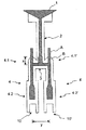
図1に示した装置は、マイクロ波源(ここでは図示せず)が接続される上部領域が示されており、下部領域はコーティング室を備える。この場合、装置は、内部導体Aおよび外部導体Bを備えた同軸構造を備える。内部導体Aは金属からなり、外部導体Bは誘電体で、この場合、空隙である。誘電体は、金属表面により境界を画される。本発明の状況(context)では、誘電体は、非金属媒体または金属性導電媒体を意味するものと理解されたい。したがって、本明細書で用いられた状況では、誘電体という用語は、たとえば空気または真空のような媒体も包含する。 The apparatus shown in FIG. 1 shows an upper region to which a microwave source (not shown here) is connected, and the lower region comprises a coating chamber. In this case, the device comprises a coaxial structure with an inner conductor A and an outer conductor B. The inner conductor A is made of metal, and the outer conductor B is a dielectric. In this case, it is a gap. The dielectric is bounded by the metal surface. In the context of the present invention, dielectric is to be understood as meaning a non-metallic medium or a metallic conductive medium. Thus, in the context used herein, the term dielectric also encompasses media such as air or vacuum.
この場合では、2つの処理室10、10’が設けられて、単一のマイクロ波源により供給される。この場合では、コーティング室が基材自体(たとえばガラスバイアル)から形成され、コーティング室がそれぞれガスノズル(図示せず)を割り当てられるか、あるいはそれぞれ1つの基材(たとえば外部コーティング用)がコーティング室の1つに収容される。処理されるべき基材は同じタイプであることが好ましい。ガラスのバイアルまたはボトルの代替として、プラスチックのバイアルまたはボトルまたはリフレクタも考慮されてよい。
In this case, two
上述の同軸導体構造の幾何学構造は、円錐1がマイクロ波源MwQ(詳細には図示せず)に接続されるように構成される。この円錐は、矩形導波管(ここでは図示せず)から上述の同軸導体構造への移行を形成するために用いられる。
The geometric structure of the coaxial conductor structure described above is configured such that the
導体2が円錐1に接続されている。H字形導体構造が導体2に接合している。このH字形導体構造は、ウェブ3および2つのリム4、4’を備える。この2つのリムは、上リム部4.1および下リム部4.2または上リム部4.1’および下リム部4.2’からなる。
A
コーティング室への供給導体、またはインピーダンス構造、特に導体2およびH字形導体構造は、固定または剛性導体として設計される。これにより、導体の位置が決まるため、電磁エネルギーの伝導および分割は、導体が動くことによる影響を受けることがない。
The supply conductor to the coating chamber, or the impedance structure, in particular the
以下で扱われるであろう寸法xが重要である。この寸法は、誘電体Bで囲われたリム部4.1または4.1’の長さの部分を示す。 The dimension x, which will be dealt with below, is important. This dimension indicates the length of the rim part 4.1 or 4.1 'surrounded by the dielectric B.
さらに重要な寸法は、下リム部4.2、4.2’間の距離y、すなわち処理室10、10’の領域にあるリム部間の距離である。本発明者らは、上記のパラメータxおよびyを適切に選択することで、処理室(コーティング室)の割合を調整することができ、処理室ごとに品質が異なることをなくすとともに許容可能なコーティング品質がすべての基材上に達成することができることを見い出した。
A further important dimension is the distance y between the lower rim parts 4.2, 4.2 ', i.e. the distance between the rim parts in the region of the
したがって、本発明のシステムにより、ダブルコーティングステーションまたはマルチコーティングステーションを提供することが可能となり、そのため生産量が大幅に増すとともに生産コストが大幅に低減される。この結果として、特にエネルギーコストが低減されることができる。コーティング品質が最適化されることができる。 Thus, the system of the present invention makes it possible to provide a double coating station or a multi-coating station, thereby greatly increasing production and reducing production costs. As a result, energy costs can be reduced in particular. The coating quality can be optimized.
この状況で、上述の2つのパラメータx、yのうち、調整を行うには一方のみを変更すればよいことを強調しておく。パラメータxは特に重要である。 In this situation, it is emphasized that only one of the two parameters x and y described above needs to be changed for adjustment. The parameter x is particularly important.
図2は、実際にこの調整を実施することができる方法を示す。この図もまた、同軸導体構造を示すとともに、H字形の幾何学構造も示す。 FIG. 2 shows how this adjustment can actually be performed. This figure also shows a coaxial conductor structure and an H-shaped geometric structure.
2つのリム部4.1、4.1’は、それぞれスリーブ5、5’で囲われている。これらのスリーブは、リム部に沿って変位することができる。この変位により、導体構造の電気長を変えることができる。この変更はリム部ごとに異なるため、このようにしてコーティング室10、10’のコーティング品質に影響を与えることができる。リム部4.1または4.1’それぞれに沿ったスリーブ5、5’の変位は、この実施形態では、調整装置43または43’それぞれにより行われ、各調整装置はそれぞれ、スリーブ5、5’それぞれに接続される調整ねじ44または44’をそれぞれ備える。
The two rim parts 4.1, 4.1 'are surrounded by
スリーブの調整はまた、スリーブの設定を異ならせると、2つのリム4および4’に対して異なるパラメータxをもたらす。これらの異なるパラメータxは以下ではx1およびx2と呼ぶ。しかしながら、装置が最適に設定される場合、パラメータ値x1およびx2は概して、パラメータ間の差がインピーダンス構造の2つの経路のインピーダンス間の小さな差を補償するような程度に異なるだけであろう。したがって、均一のパラメータxを得ることができるよう、パラメータx1およびx2の平均をとることができ(x=1/2(x1+x2))、それによって精度の優れた値のxが得られる。
Adjustment of the sleeve also results in different parameters x for the two
さらに、リム4、4’に、この場合はリム部4.2、4.2’にねじ6、6’を深くまたは浅くねじ込むことによって影響を与えることもできる。
Furthermore, it is also possible to influence the
本明細書では図示していないが、入力導体部2はまた、2つのスリーブ4.1、4.1’に対応するスリーブ、または2つのねじ6、6’に対応するねじ、あるいはこれらの手段のいずれも割り当てられてよいことが理解されよう。
Although not shown in the present description, the
例として本明細書に示した同軸導体構造には次のことが当てはまる。すなわち、内部導体の所与の直径について、無反射の整合(matching)は、外部導体の非常に特異な(specific)直径およびパラメータxとパラメータyとの非常に特異な比を用いることによってのみ得られる。 The following applies to the coaxial conductor structure shown here as an example. That is, for a given diameter of the inner conductor, non-reflective matching can only be obtained by using a very specific diameter of the outer conductor and a very specific ratio of parameter x to parameter y. It is done.
特に、ほぼ無反射の整合は、パラメータyが、用いられる電磁波の半波長の倍数である場合に、すなわちy=nλ/2、n∈[1、2、3、...]の関係がほぼ満たされている場合に達成されることができることが分かっている。インピーダンス構造における電力分割に対し良好な結果を得るため、所定の制約が装置の寸法に課される。2.45GHzの周波数であっても同軸導体の波長は12cmを上回るので、この周波数および構造が用いられる場合、距離yはもっぱら約6cmの整数倍として選択されることができる。さらに、波長もまた、同軸導体を用いるか導波管を用いるかによって決まる。同軸導体の場合、波長は真空波長に近い。R26導波管構造の場合、たとえば、2.45GHzでの波長は約17.4cmであるため、この場合の最適な設定では、yは約8.7cmであるべきである。 In particular, the nearly non-reflective matching is when the parameter y is a multiple of the half-wavelength of the electromagnetic wave used, i.e. y = nλ / 2, nε [1,2,3,. . . It has been found that this can be achieved if the relationship is nearly satisfied. In order to obtain good results for power splitting in an impedance structure, certain constraints are imposed on the dimensions of the device. Since the wavelength of the coaxial conductor exceeds 12 cm even at a frequency of 2.45 GHz, if this frequency and structure is used, the distance y can be chosen exclusively as an integer multiple of about 6 cm. Furthermore, the wavelength also depends on whether a coaxial conductor or a waveguide is used. In the case of a coaxial conductor, the wavelength is close to the vacuum wavelength. For the R26 waveguide structure, for example, the wavelength at 2.45 GHz is about 17.4 cm, so in the optimal setting in this case, y should be about 8.7 cm.
時として、CVD法においていっそう低い周波数が選択されるため、対応する波長はいっそう長くなる。特に均一なコーティングを得るための、たとえば広域のコーティングの場合等の所定の用途に対してPICVD法では、より低い周波数もまた用いられる。したがって、波長が長くなるにつれて、コーティング装置に対する関連する設計上の制約も多くなる。 Sometimes, lower frequencies are selected in the CVD method, so the corresponding wavelength is longer. Lower frequencies are also used in PICVD methods for certain applications, for example in the case of wide area coatings, to obtain a particularly uniform coating. Therefore, as the wavelength increases, the associated design constraints on the coating equipment also increase.
しかしながら、これらの制約は、インピーダンス構造が追加のリムを有する場合に回避できることが分かっている。この形式の実施形態は、図3Aないし図3Dに示されている。図3Aないし図3Dを参照して示す実施形態では、図1および図2を参照して説明した例示的な実施形態と同様に、単一のマイクロ波源からのマイクロ波エネルギーがインピーダンス分岐に分割される。 However, it has been found that these constraints can be avoided if the impedance structure has an additional rim. This type of embodiment is illustrated in FIGS. 3A-3D. In the embodiment shown with reference to FIGS. 3A-3D, as in the exemplary embodiment described with reference to FIGS. 1 and 2, the microwave energy from a single microwave source is divided into impedance branches. The
図3Aおよび図3Bに示した装置も同様に、内部導体Aおよび外部導体Bを有する同軸構造を備える。内部導体Aは、好ましくは、金属からなり、外部導体Bは導電面により境界を画される誘電体(たとえば空隙)からなる。 The device shown in FIGS. 3A and 3B similarly includes a coaxial structure having an inner conductor A and an outer conductor B. The inner conductor A is preferably made of metal, and the outer conductor B is made of a dielectric (for example, an air gap) delimited by a conductive surface.
インピーダンス構造によって分割された、マイクロ波源からのマイクロ波エネルギーは、処理室10、10’に供給するために用いられる。
The microwave energy from the microwave source divided by the impedance structure is used to supply the
上述の実施形態と同様に、ウェブ3および2つのリム4、4’を有するH字形導体構造は、導体2に接続されている。上述の実施形態とは異なり、インピーダンス構造は、ウェブ3に接続される追加のリム7を有する。
Similar to the embodiment described above, the H-shaped conductor structure having the
リム7は、ウェブ3の中央を始端とした、誘電体Bを満たす空隙の長さを示すパラメータzを定める。この実施形態では、リムは、導体2と同様に、2つのリム4および4’の間でウェブ3の中央に取り付けられる。
The
さらに、リム7は、リム7と導体2が位置合わせされるようにウェブ3に対し導体2と反対側に配置される。しかしながら、この配置は絶対に必要というわけではない。リム7および導体2が互いにある角度、たとえば約90°にある2つの方向に延びることもできる。この特徴を持つ実施形態では、導体2、ウェブ3、およびリム7は、互いに略垂直な3つの方向に延びる。
Further, the
図3Bは、図3Aで示した追加のリム7を有する実施形態の詳細を示す。同軸導体構造は、追加のリム7が横棒についたH字形の幾何学構造を有する。
FIG. 3B shows details of the embodiment with the
2つのリム部4.1、4.1’およびリム7はそれぞれスリーブ5、5’および71で囲われており、これらのスリーブは、調整装置43、43’、73によりリム部4.1、4.1’、またはリム7に沿って変位することができる。図1および図2を参照して示した実施形態と同様に、リム部4.1、4.1’の電気長はそれぞれ、調整装置43および43’により別個に変更することができる。この実施形態では、調整装置73により、他の設定とは別個にリム7の電気長を設定することも可能である。これにより、パラメータx、x’およびzを別個に設定することができるとともに、マイクロ波電力の均一な分割を達成することができるようになる。
The two rim parts 4.1, 4.1 'and the
図3Cおよび図3Dは、図3Aおよび図3Bを参照して示した実施形態の変形形態を示す。この変形形態では、インピーダンス構造は、図3Aおよび図3Bで示した同軸導体の代わりに導波管を備える。導波管は、円形導波管および矩形導波管のどちらを備えていてよい。導波管を有するこのような変形形態は、比較的高い周波数の場合に特に適している。 3C and 3D show a variation of the embodiment shown with reference to FIGS. 3A and 3B. In this variation, the impedance structure comprises a waveguide instead of the coaxial conductor shown in FIGS. 3A and 3B. The waveguide may comprise either a circular waveguide or a rectangular waveguide. Such a variant with a waveguide is particularly suitable for relatively high frequencies.
この変形形態はまた、パラメータx1、x2、およびzを、リム部4.1、4.1’、およびリム7に沿ってそれぞれ変位されることができるスリーブ5、5’、および71により調整かつ最適化することができる。
This variant also adjusts the parameters x1, x2, and z by means of
図3Dに示すように、コーティング室10、10’はたとえば、コーティングされるべきワークピース(work piece)によって形成されてよい。この場合、図3Dは、導体構造に結合され、そこを通ってマイクロ波がアンプルの内部に入るアンプルのベース領域を示している。アンプルのほかに、たとえばバイアル、ボトル、または球状キャップ等の中空体形状の他のワークピースの内部をコーティングすることもでき、あるいは、たとえばランプ球(lamp bulb)等の他のワークピースの外部を別個のコーティング室でコーティングすることもできる。この場合もまた、コーティング室10、10’への供給導体またはインピーダンス構造、特に導体2およびH字形導体構造が、固定または剛性導体として設計される。
As shown in FIG. 3D, the
図3Bおよび図3Dに示すように、すべての実施形態では、マイクロ波を誘電体窓8、8’を介してコーティング室10、10’に導入することができる。この誘電体窓により、プラズマがインピーダンス構造または導波管構造においてプラズマが点火することが防止されるが、この理由はプロセスガスの浸透が回避されるか、あるいはプラズマが点火しない圧力に維持することができるからである。
As shown in FIGS. 3B and 3D, in all embodiments, microwaves can be introduced into the
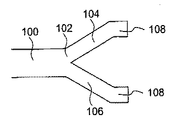
図4Aおよび図4B、ならびに図5は、マイクロ波源(図示せず)により発生するマイクロ波エネルギーの分割が、マイクロ波エネルギーが導波管100内にあるうちに行われる、本発明の実施形態を示す。マイクロ波源からのマイクロ波エネルギーはすべて、導波管100(たとえば矩形導波管)へ導入され、図示の実施形態の領域102で2つの部分に分割される。マイクロ波エネルギーの一部は矩形導波管104に送られ、もう一部は矩形導波管106へ送られる。これらの分岐104および106に導入されたマイクロ波エネルギーは、矩形導波管108に送られる。図4Bに示す矩形導波管108では、マイクロ波エネルギーは、同軸導体110を介して、コーティングされるべき個々のコーティング室112(この場合、事実上の3D(3次元)容器であってよい)導入される。本プロセスを用いてコーティングすることができる3D容器の例として、球状キャップ、シリンジ、アンプル、ボトル、バイアル、カテーテルが挙げられる。本発明の場合、各3D容器112が専用の真空供給源114および専用のガス供給源116を有することが重要である。専用の供給デバイスにより、マルチステーションコーティングシステムの個々のコーティング室が分離してすなわち個々に動作または制御することが可能となる。
4A and 4B, and FIG. 5 illustrate an embodiment of the present invention in which the division of microwave energy generated by a microwave source (not shown) is performed while the microwave energy is in the
個々のコーティング室それぞれが、パルスモードで個々に動作するように、プラズマまたはコーティングされるべき基材にから発生する熱放射および/または電磁放射を検知する分離したプラズマ監視装置118も有することが特に有利である。
In particular, each individual coating chamber also has a separate
図4Bに示すようにエネルギーが同軸導体によって導入される以外に、図5に示すように、分割した導波管の個々の分岐104および106のエネルギーを、誘電体窓として知られるものによって個々のコーティング室112.1および112.2に導入することもできる。
In addition to the energy introduced by the coaxial conductor as shown in FIG. 4B, as shown in FIG. 5, the energy of the
示した実施形態を組合わせることも可能である。 It is also possible to combine the embodiments shown.
図6および図7は、3つ以上のコーティングステーションを実現することが可能な本発明の例を示している。このことは、同軸導体および導波管のいずれを用いることでも可能である。 Figures 6 and 7 show examples of the present invention in which more than two coating stations can be realized. This is possible by using either a coaxial conductor or a waveguide.
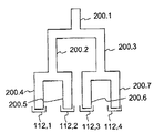
図6に示す実施形態では、本発明に従って、第1の同軸導体200.1は、2つの同軸導体200.2、200.3に分割される。同軸導体200.2、200.3は、次に、分岐カスケードの形式で2つの同軸導体または導波管200.4、200.5、200.6、200.7に分割される。個々のコーティング室112.1、112.2、112.3、112.4は分岐カスケードの端部に設置される。 In the embodiment shown in FIG. 6, in accordance with the present invention, the first coaxial conductor 200.1 is divided into two coaxial conductors 200.2, 200.3. The coaxial conductors 200.2, 200.3 are then divided into two coaxial conductors or waveguides 200.4, 200.5, 200.6, 200.7 in the form of a branch cascade. Individual coating chambers 112.1, 112.2, 112.3, 112.4 are installed at the end of the branch cascade.
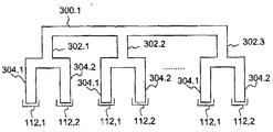
図6に示したカスケード状構成の代替として、それぞれが2つの矩形導波管または2つの同軸導体304.1、304.2を有する複数のダブルステーション302.1、302.2、302.3が共通の導波管300.1に接続されることも考えられてよい。コーティング室112.1、112.2が、それぞれ対応する同軸導体または導波管304.1、304.2の下側に配置される。 As an alternative to the cascaded configuration shown in FIG. 6, a plurality of double stations 302.1, 302.2, 302.3 each having two rectangular waveguides or two coaxial conductors 304.1, 304.2 are provided. It may also be conceivable to be connected to a common waveguide 300.1. Coating chambers 112.1, 112.2 are arranged below the corresponding coaxial conductors or waveguides 304.1, 304.2, respectively.
本発明は初めて、複数のコーティング室が単一のマイクロ波源を用いて動作することを可能にする、物品をコーティングする装置を提案する。 The present invention for the first time proposes an apparatus for coating articles that allows multiple coating chambers to operate using a single microwave source.
本発明は、パルス状あるいは非パルス状のマイクロ波エネルギーが、適当な分割によって用いられ、エネルギーを複数の分離したコーティングステーションに供給することを可能にする。コーティング技術上、たとえば隣接したコーティングステーションが互いに影響を及ぼし合うことを防止するため、コーティングステーションは、互いから分離したままであるが、1つのエネルギー源によって供給される。本発明により、あるコーティング室から別のコーティング室への交互の点火、すなわち統制されていない点火が起るのではなく、コーティング室すべてが同時に点火し、それと同じエネルギーの供給がコーティング持続期間中に維持される。 The present invention allows pulsed or non-pulsed microwave energy to be used with appropriate splitting to deliver energy to multiple separate coating stations. In coating technology, for example, to prevent adjacent coating stations from affecting each other, the coating stations remain separated from each other but are supplied by one energy source. In accordance with the present invention, instead of alternating ignition from one coating chamber to another, i.e. uncontrolled ignition, all coating chambers ignite simultaneously and the same supply of energy is applied during the coating duration. Maintained.
本発明による装置では、プラズマ体積およびガス組成は必ずしも重要ではない。本装置により、アンプルのコーティングに対し2ml〜10mlのプラズマ体積を用いる内部コーティング、約50mlのプラズマ体積を用いる球状キャップの内部コーティング、および最大100mlのプラズマ体積を用いるランプ球の外部コーティングのいずれも、プロセスパラメータを再調整する必要なく生成することが可能となる。インピーダンスの大幅な変更は、プラスマ体積の変化に関連する。さらに、異なるプラズマの体積に対して、異なるガス組成、特に異なる前駆体(たとえばヘキサメチルジシロキサンまたは塩化チタン)を有するガス組成を、それぞれの場合に、異なる濃度で、プラズマ特性およびコーティング品質を大幅に変えることがなく用いることが可能であり、このガス組成も、インピーダンスにかなりの影響を与える。 In the device according to the invention, the plasma volume and the gas composition are not necessarily important. With this apparatus, the inner coating using a plasma volume of 2 ml to 10 ml for the coating of the ampoule, the inner coating of a spherical cap using a plasma volume of about 50 ml, and the outer coating of a lamp bulb using a plasma volume of up to 100 ml, Process parameters can be generated without having to readjust. A significant change in impedance is associated with a change in plasma volume. In addition, for different plasma volumes, gas compositions with different gas compositions, especially with different precursors (eg hexamethyldisiloxane or titanium chloride), in each case with different concentrations, greatly increase plasma properties and coating quality. The gas composition also has a significant effect on the impedance.
Claims (20)
単一のマイクロ波源、および
2つ以上のコーティング室(10、10’)を有し、
前記コーティング室(10、10’)がすべて単一のマイクロ波源に接続され、
前記個々のコーティング室(10、10’)にプラズマを発生させるためにマイクロ波エネルギーを分割するための、同軸導体構造体又は導波管構造体からなるインピーダンス構造体を有し、
前記同軸導体構造体又は前記導波管構造体が、ウェブ(3)および2つのリム(4、4’)を含むH字形導体構造体を備え、
前記H字形導体構造体が少なくとも2つのコーティング室(10、10’)の上流に接続され、
前記ウェブ(3)が入力導体(2)を介して前記マイクロ波源に接続され、
前記H字形導体構造体の各リム(4、4’)が、対応する前記コーティング室(10、10’)から離隔している部分(4.1、4.1’)および該コーティング室(10、10’)の1つに面する部分(4.2、4.2’)を有し、
前記対応するコーティング室(10、10’)から離隔している前記リム部の電気長が調整可能である装置。An apparatus for coating an article,
Having a single microwave source, and two or more coating chambers (10, 10 '),
The coating chambers (10, 10 ') are all connected to a single microwave source;
An impedance structure comprising a coaxial conductor structure or a waveguide structure for dividing microwave energy to generate plasma in the individual coating chambers (10, 10 ');
The coaxial conductor structure or the waveguide structure comprises an H-shaped conductor structure comprising a web (3) and two rims (4, 4 ') ;
The H-shaped conductor structure is connected upstream of at least two coating chambers (10, 10 ');
The web (3) is connected to the microwave source via an input conductor (2);
Each rim (4, 4 ′) of the H-shaped conductor structure is spaced from the corresponding coating chamber (10, 10 ′) (4.1, 4.1 ′) and the coating chamber (10 10 ′) facing one part (4.2, 4.2 ′)
An apparatus in which the electrical length of the rim part spaced from the corresponding coating chamber (10, 10 ') is adjustable.
Applications Claiming Priority (3)
| Application Number | Priority Date | Filing Date | Title |
|---|---|---|---|
| DE10138693A DE10138693A1 (en) | 2001-08-07 | 2001-08-07 | Device for coating objects |
| DE10138693.1 | 2001-08-07 | ||
| PCT/EP2002/008852 WO2003015122A1 (en) | 2001-08-07 | 2002-08-07 | Device for the coating of objects |
Publications (3)
| Publication Number | Publication Date |
|---|---|
| JP2004538367A JP2004538367A (en) | 2004-12-24 |
| JP2004538367A5 JP2004538367A5 (en) | 2005-12-22 |
| JP4732685B2 true JP4732685B2 (en) | 2011-07-27 |
Family
ID=7694632
Family Applications (1)
| Application Number | Title | Priority Date | Filing Date |
|---|---|---|---|
| JP2003519960A Expired - Lifetime JP4732685B2 (en) | 2001-08-07 | 2002-08-07 | Equipment for coating articles |
Country Status (7)
| Country | Link |
|---|---|
| US (1) | US7434537B2 (en) |
| EP (1) | EP1415321B1 (en) |
| JP (1) | JP4732685B2 (en) |
| CN (1) | CN1328751C (en) |
| AT (1) | ATE295612T1 (en) |
| DE (2) | DE10138693A1 (en) |
| WO (1) | WO2003015122A1 (en) |
Families Citing this family (29)
| Publication number | Priority date | Publication date | Assignee | Title |
|---|---|---|---|---|
| DE10358329B4 (en) | 2003-12-12 | 2007-08-02 | R3T Gmbh Rapid Reactive Radicals Technology | Device for generating excited and / or ionized particles in a plasma and method for producing ionized particles |
| US7791280B2 (en) * | 2005-10-27 | 2010-09-07 | Luxim Corporation | Plasma lamp using a shaped waveguide body |
| US7825669B2 (en) * | 2007-03-29 | 2010-11-02 | Hamilton Sundstrand Corporation | Microwave position sensing for a turbo machine |
| CN101632330B (en) * | 2007-06-11 | 2012-11-21 | 东京毅力科创株式会社 | Plasma processing apparatus, power supply apparatus and method for using plasma processing apparatus |
| JP5324138B2 (en) * | 2008-06-11 | 2013-10-23 | 東京エレクトロン株式会社 | Plasma processing apparatus and plasma processing method |
| JP5324137B2 (en) * | 2008-06-11 | 2013-10-23 | 東京エレクトロン株式会社 | Plasma processing apparatus and plasma processing method |
| WO2009150971A1 (en) * | 2008-06-11 | 2009-12-17 | 東京エレクトロン株式会社 | Plasma processing apparatus and plasma processing method |
| WO2010067590A1 (en) * | 2008-12-11 | 2010-06-17 | 東洋製罐株式会社 | Microwave plasma treatment device |
| JP5222744B2 (en) * | 2009-01-21 | 2013-06-26 | 国立大学法人東北大学 | Plasma processing equipment |
| JP2012089334A (en) | 2010-10-19 | 2012-05-10 | Tokyo Electron Ltd | Microwave plasma source and plasma processing apparatus |
| GB201021855D0 (en) | 2010-12-23 | 2011-02-02 | Element Six Ltd | Microwave power delivery system for plasma reactors |
| GB201021870D0 (en) | 2010-12-23 | 2011-02-02 | Element Six Ltd | A microwave plasma reactor for manufacturing synthetic diamond material |
| GB201021913D0 (en) | 2010-12-23 | 2011-02-02 | Element Six Ltd | Microwave plasma reactors and substrates for synthetic diamond manufacture |
| GB201021853D0 (en) | 2010-12-23 | 2011-02-02 | Element Six Ltd | A microwave plasma reactor for manufacturing synthetic diamond material |
| GB201021865D0 (en) | 2010-12-23 | 2011-02-02 | Element Six Ltd | A microwave plasma reactor for manufacturing synthetic diamond material |
| GB201021860D0 (en) | 2010-12-23 | 2011-02-02 | Element Six Ltd | A microwave plasma reactor for diamond synthesis |
| US9637838B2 (en) | 2010-12-23 | 2017-05-02 | Element Six Limited | Methods of manufacturing synthetic diamond material by microwave plasma enhanced chemical vapor deposition from a microwave generator and gas inlet(s) disposed opposite the growth surface area |
| CN105244251B (en) * | 2015-11-03 | 2017-11-17 | 长飞光纤光缆股份有限公司 | A kind of high power plasma microwave cavity |
| CN105502918B (en) * | 2015-12-25 | 2019-01-25 | 长飞光纤光缆股份有限公司 | A kind of dual-chamber type plasma microwave cavity |
| CN106229595A (en) * | 2016-08-30 | 2016-12-14 | 广东通宇通讯股份有限公司 | Power dividers and their components |
| CA3065360A1 (en) * | 2017-05-30 | 2018-12-06 | Ellume Limited | Nanoparticle aggregates |
| JP2022151858A (en) | 2021-03-25 | 2022-10-07 | ショット シュヴァイツ アー・ゲー | Test method for quality evaluation and coated container |
| EP4063334A1 (en) | 2021-03-25 | 2022-09-28 | Schott Ag | Coated glass element |
| US12269645B2 (en) | 2021-03-25 | 2025-04-08 | Schott Ag | Coated glass element |
| EP4067318A3 (en) | 2021-03-25 | 2022-10-26 | Schott Ag | Coated glass element |
| EP4313894A1 (en) | 2021-03-25 | 2024-02-07 | SCHOTT Pharma AG & Co. KGaA | Pharmaceutical container |
| KR102765720B1 (en) * | 2021-10-20 | 2025-02-14 | 세메스 주식회사 | Apparatus for treating substrate and method for operating there of |
| KR102752563B1 (en) * | 2022-06-14 | 2025-01-10 | 세메스 주식회사 | Microwave providing apparatus, system including the same and method of manufacturing semiconductor device |
| EP4339171A1 (en) | 2022-09-13 | 2024-03-20 | Schott Ag | Treatment of a glass container |
Family Cites Families (22)
| Publication number | Priority date | Publication date | Assignee | Title |
|---|---|---|---|---|
| JPS5888086A (en) * | 1981-11-20 | 1983-05-26 | Sanki Eng Co Ltd | Apparatus for heat-treating waste matter |
| JPS61220486A (en) * | 1985-03-27 | 1986-09-30 | Mitsubishi Electric Corp | Laser oscillation device |
| JPH0616496B2 (en) * | 1986-09-24 | 1994-03-02 | 日本電気株式会社 | Excited seed CVD device |
| DE3711184A1 (en) * | 1987-04-02 | 1988-10-20 | Leybold Ag | DEVICE FOR THE APPLICATION OF MICROWAVE ENERGY WITH AN OPEN MICROWAVE LEAD |
| US4985227A (en) * | 1987-04-22 | 1991-01-15 | Indemitsu Petrochemical Co., Ltd. | Method for synthesis or diamond |
| DE68926923T2 (en) * | 1988-03-16 | 1996-12-19 | Hitachi Ltd | Microwave ion source |
| JPH02148715A (en) * | 1988-11-29 | 1990-06-07 | Canon Inc | Apparatus for forming semiconductor device continuously |
| US5202095A (en) | 1988-12-27 | 1993-04-13 | Matsushita Electric Industrial Co., Ltd. | Microwave plasma processor |
| US5236511A (en) * | 1990-03-16 | 1993-08-17 | Schott Glaswerke | Plasma CVD process for coating a dome-shaped substrate |
| US5103182A (en) * | 1990-04-02 | 1992-04-07 | Texas Instruments Incorporated | Electromagnetic wave measurement of conductive layers of a semiconductor wafer during processing in a fabrication chamber |
| DE4120176C1 (en) * | 1991-06-19 | 1992-02-27 | Schott Glaswerke, 6500 Mainz, De | |
| DE4136297A1 (en) * | 1991-11-04 | 1993-05-06 | Plasma Electronic Gmbh, 7024 Filderstadt, De | Localised plasma prodn. in treatment chamber - using microwave generator connected to coupling device which passes through the wall of the chamber without using a coupling window |
| US5311103A (en) * | 1992-06-01 | 1994-05-10 | Board Of Trustees Operating Michigan State University | Apparatus for the coating of material on a substrate using a microwave or UHF plasma |
| DE69318480T2 (en) * | 1992-06-23 | 1998-09-17 | Nippon Telegraph & Telephone | Plasma processing device |
| US5387288A (en) * | 1993-05-14 | 1995-02-07 | Modular Process Technology Corp. | Apparatus for depositing diamond and refractory materials comprising rotating antenna |
| DE19628949B4 (en) * | 1995-02-02 | 2008-12-04 | Muegge Electronic Gmbh | Device for generating plasma |
| DE19503205C1 (en) | 1995-02-02 | 1996-07-11 | Muegge Electronic Gmbh | Device for generating a plasma in low pressure container e.g. for hardware items surface treatment by plasma etching and plasma deposition |
| DE19608949A1 (en) * | 1996-03-08 | 1997-09-11 | Ralf Dr Spitzl | Device for generating powerful microwave plasmas |
| US5874706A (en) * | 1996-09-26 | 1999-02-23 | Tokyo Electron Limited | Microwave plasma processing apparatus using a hybrid microwave having two different modes of oscillation or branched microwaves forming a concentric electric field |
| US6186090B1 (en) * | 1999-03-04 | 2001-02-13 | Energy Conversion Devices, Inc. | Apparatus for the simultaneous deposition by physical vapor deposition and chemical vapor deposition and method therefor |
| DE19916478A1 (en) * | 1999-04-13 | 2000-10-19 | Ruediger Haaga Gmbh | Procedure for evacuation of a container in which a plasma discharge it to be set up in a plasma reactor for sterilization of components has a multi-stage pumping process with vacuum pumps efficient over different pressures |
| JP3792089B2 (en) * | 2000-01-14 | 2006-06-28 | シャープ株式会社 | Plasma process equipment |
-
2001
- 2001-08-07 DE DE10138693A patent/DE10138693A1/en not_active Withdrawn
-
2002
- 2002-08-07 EP EP02767344A patent/EP1415321B1/en not_active Expired - Lifetime
- 2002-08-07 WO PCT/EP2002/008852 patent/WO2003015122A1/en not_active Ceased
- 2002-08-07 US US10/486,140 patent/US7434537B2/en not_active Expired - Lifetime
- 2002-08-07 CN CNB028154231A patent/CN1328751C/en not_active Expired - Lifetime
- 2002-08-07 JP JP2003519960A patent/JP4732685B2/en not_active Expired - Lifetime
- 2002-08-07 DE DE50203097T patent/DE50203097D1/en not_active Expired - Lifetime
- 2002-08-07 AT AT02767344T patent/ATE295612T1/en not_active IP Right Cessation
Also Published As
| Publication number | Publication date |
|---|---|
| DE10138693A1 (en) | 2003-07-10 |
| CN1328751C (en) | 2007-07-25 |
| US20050005853A1 (en) | 2005-01-13 |
| DE50203097D1 (en) | 2005-06-16 |
| WO2003015122A1 (en) | 2003-02-20 |
| CN1539155A (en) | 2004-10-20 |
| EP1415321A1 (en) | 2004-05-06 |
| EP1415321B1 (en) | 2005-05-11 |
| ATE295612T1 (en) | 2005-05-15 |
| JP2004538367A (en) | 2004-12-24 |
| US7434537B2 (en) | 2008-10-14 |
Similar Documents
| Publication | Publication Date | Title |
|---|---|---|
| JP4732685B2 (en) | Equipment for coating articles | |
| US11721532B2 (en) | Modular microwave source with local lorentz force | |
| TWI719290B (en) | Plasma processing tool using modular microwave sources | |
| JP4116454B2 (en) | Apparatus for plasma treatment of dielectric objects | |
| US20200381217A1 (en) | Modular microwave plasma source | |
| US6396214B1 (en) | Device for producing a free cold plasma jet | |
| KR102029579B1 (en) | Plasma processing apparatus and control method | |
| CN110391125B (en) | Modular high-frequency source with integrated gas distribution | |
| JP2004538367A5 (en) | ||
| JP2002275635A (en) | Process and apparatus for microwave plasma treatment | |
| US11114282B2 (en) | Phased array modular high-frequency source | |
| KR102918592B1 (en) | Modular high-frequency source | |
| JP2007231386A (en) | Container processing equipment using plasma | |
| JP6501493B2 (en) | Plasma processing system | |
| US20070095281A1 (en) | System and method for power function ramping of microwave liner discharge sources | |
| US20090152243A1 (en) | Plasma processing apparatus and method thereof | |
| US10290471B2 (en) | Device for generating plasma by means of microwaves | |
| WO2016104205A1 (en) | Plasma processing device and plasma processing method | |
| WO2022044864A1 (en) | Plasma processing device, plasma processing method, and dielectric window | |
| CN120188256A (en) | Microwave plasma reactor with multiple emitters and absorbers and method for plasma processing a workpiece using the microwave plasma reactor | |
| JP2006089846A (en) | Microwave processing apparatus, microwave supply / processing system, and microwave processing method |
Legal Events
| Date | Code | Title | Description |
|---|---|---|---|
| A521 | Request for written amendment filed |
Free format text: JAPANESE INTERMEDIATE CODE: A523 Effective date: 20041019 |
|
| A621 | Written request for application examination |
Free format text: JAPANESE INTERMEDIATE CODE: A621 Effective date: 20041019 |
|
| A711 | Notification of change in applicant |
Free format text: JAPANESE INTERMEDIATE CODE: A711 Effective date: 20050831 |
|
| RD03 | Notification of appointment of power of attorney |
Free format text: JAPANESE INTERMEDIATE CODE: A7423 Effective date: 20051018 |
|
| RD04 | Notification of resignation of power of attorney |
Free format text: JAPANESE INTERMEDIATE CODE: A7424 Effective date: 20051205 |
|
| A977 | Report on retrieval |
Free format text: JAPANESE INTERMEDIATE CODE: A971007 Effective date: 20071121 |
|
| A131 | Notification of reasons for refusal |
Free format text: JAPANESE INTERMEDIATE CODE: A131 Effective date: 20071205 |
|
| A601 | Written request for extension of time |
Free format text: JAPANESE INTERMEDIATE CODE: A601 Effective date: 20080305 |
|
| A602 | Written permission of extension of time |
Free format text: JAPANESE INTERMEDIATE CODE: A602 Effective date: 20080312 |
|
| A601 | Written request for extension of time |
Free format text: JAPANESE INTERMEDIATE CODE: A601 Effective date: 20080404 |
|
| A602 | Written permission of extension of time |
Free format text: JAPANESE INTERMEDIATE CODE: A602 Effective date: 20080411 |
|
| A601 | Written request for extension of time |
Free format text: JAPANESE INTERMEDIATE CODE: A601 Effective date: 20080502 |
|
| A602 | Written permission of extension of time |
Free format text: JAPANESE INTERMEDIATE CODE: A602 Effective date: 20080513 |
|
| A521 | Request for written amendment filed |
Free format text: JAPANESE INTERMEDIATE CODE: A523 Effective date: 20080605 |
|
| A02 | Decision of refusal |
Free format text: JAPANESE INTERMEDIATE CODE: A02 Effective date: 20081008 |
|
| A521 | Request for written amendment filed |
Free format text: JAPANESE INTERMEDIATE CODE: A523 Effective date: 20090205 |
|
| A911 | Transfer to examiner for re-examination before appeal (zenchi) |
Free format text: JAPANESE INTERMEDIATE CODE: A911 Effective date: 20090226 |
|
| A912 | Re-examination (zenchi) completed and case transferred to appeal board |
Free format text: JAPANESE INTERMEDIATE CODE: A912 Effective date: 20090417 |
|
| A521 | Request for written amendment filed |
Free format text: JAPANESE INTERMEDIATE CODE: A523 Effective date: 20110302 |
|
| A61 | First payment of annual fees (during grant procedure) |
Free format text: JAPANESE INTERMEDIATE CODE: A61 Effective date: 20110421 |
|
| FPAY | Renewal fee payment (event date is renewal date of database) |
Free format text: PAYMENT UNTIL: 20140428 Year of fee payment: 3 |
|
| R150 | Certificate of patent or registration of utility model |
Ref document number: 4732685 Country of ref document: JP Free format text: JAPANESE INTERMEDIATE CODE: R150 Free format text: JAPANESE INTERMEDIATE CODE: R150 |
|
| R250 | Receipt of annual fees |
Free format text: JAPANESE INTERMEDIATE CODE: R250 |
|
| R250 | Receipt of annual fees |
Free format text: JAPANESE INTERMEDIATE CODE: R250 |
|
| R250 | Receipt of annual fees |
Free format text: JAPANESE INTERMEDIATE CODE: R250 |
|
| R250 | Receipt of annual fees |
Free format text: JAPANESE INTERMEDIATE CODE: R250 |
|
| R250 | Receipt of annual fees |
Free format text: JAPANESE INTERMEDIATE CODE: R250 |
|
| R250 | Receipt of annual fees |
Free format text: JAPANESE INTERMEDIATE CODE: R250 |
|
| R250 | Receipt of annual fees |
Free format text: JAPANESE INTERMEDIATE CODE: R250 |
|
| R250 | Receipt of annual fees |
Free format text: JAPANESE INTERMEDIATE CODE: R250 |
|
| R250 | Receipt of annual fees |
Free format text: JAPANESE INTERMEDIATE CODE: R250 |
|
| EXPY | Cancellation because of completion of term |