JP6501493B2 - Plasma processing system - Google Patents
Plasma processing system Download PDFInfo
- Publication number
- JP6501493B2 JP6501493B2 JP2014225390A JP2014225390A JP6501493B2 JP 6501493 B2 JP6501493 B2 JP 6501493B2 JP 2014225390 A JP2014225390 A JP 2014225390A JP 2014225390 A JP2014225390 A JP 2014225390A JP 6501493 B2 JP6501493 B2 JP 6501493B2
- Authority
- JP
- Japan
- Prior art keywords
- processing space
- gas
- processing
- injection hole
- side wall
- Prior art date
- Legal status (The legal status is an assumption and is not a legal conclusion. Google has not performed a legal analysis and makes no representation as to the accuracy of the status listed.)
- Active
Links
- 238000012545 processing Methods 0.000 title claims description 216
- 238000002347 injection Methods 0.000 claims description 128
- 239000007924 injection Substances 0.000 claims description 128
- 239000004020 conductor Substances 0.000 claims description 61
- 230000001902 propagating effect Effects 0.000 claims description 9
- 230000035699 permeability Effects 0.000 claims description 3
- 239000000243 solution Substances 0.000 claims 2
- 230000000903 blocking effect Effects 0.000 claims 1
- 239000007789 gas Substances 0.000 description 73
- 230000032258 transport Effects 0.000 description 31
- 230000005684 electric field Effects 0.000 description 26
- 238000001816 cooling Methods 0.000 description 25
- 230000002093 peripheral effect Effects 0.000 description 24
- 238000004088 simulation Methods 0.000 description 22
- 230000000979 retarding effect Effects 0.000 description 10
- 238000005516 engineering process Methods 0.000 description 5
- 238000003825 pressing Methods 0.000 description 5
- 230000005284 excitation Effects 0.000 description 4
- 239000000463 material Substances 0.000 description 4
- 238000000034 method Methods 0.000 description 4
- 238000010586 diagram Methods 0.000 description 3
- XKRFYHLGVUSROY-UHFFFAOYSA-N Argon Chemical compound [Ar] XKRFYHLGVUSROY-UHFFFAOYSA-N 0.000 description 2
- PNEYBMLMFCGWSK-UHFFFAOYSA-N aluminium oxide Inorganic materials [O-2].[O-2].[O-2].[Al+3].[Al+3] PNEYBMLMFCGWSK-UHFFFAOYSA-N 0.000 description 2
- 239000010453 quartz Substances 0.000 description 2
- VYPSYNLAJGMNEJ-UHFFFAOYSA-N silicon dioxide Inorganic materials O=[Si]=O VYPSYNLAJGMNEJ-UHFFFAOYSA-N 0.000 description 2
- 239000000758 substrate Substances 0.000 description 2
- 238000013459 approach Methods 0.000 description 1
- 229910052786 argon Inorganic materials 0.000 description 1
- 230000007423 decrease Effects 0.000 description 1
- 230000005672 electromagnetic field Effects 0.000 description 1
- 238000002474 experimental method Methods 0.000 description 1
- 238000004519 manufacturing process Methods 0.000 description 1
- 239000002184 metal Substances 0.000 description 1
- 230000000149 penetrating effect Effects 0.000 description 1
- 230000000644 propagated effect Effects 0.000 description 1
- 238000007789 sealing Methods 0.000 description 1
- 238000012546 transfer Methods 0.000 description 1
Images


Classifications
-
- H—ELECTRICITY
- H01—ELECTRIC ELEMENTS
- H01J—ELECTRIC DISCHARGE TUBES OR DISCHARGE LAMPS
- H01J37/00—Discharge tubes with provision for introducing objects or material to be exposed to the discharge, e.g. for the purpose of examination or processing thereof
- H01J37/32—Gas-filled discharge tubes
- H01J37/32431—Constructional details of the reactor
- H01J37/3244—Gas supply means
-
- H—ELECTRICITY
- H01—ELECTRIC ELEMENTS
- H01J—ELECTRIC DISCHARGE TUBES OR DISCHARGE LAMPS
- H01J37/00—Discharge tubes with provision for introducing objects or material to be exposed to the discharge, e.g. for the purpose of examination or processing thereof
- H01J37/32—Gas-filled discharge tubes
- H01J37/32009—Arrangements for generation of plasma specially adapted for examination or treatment of objects, e.g. plasma sources
- H01J37/32192—Microwave generated discharge
-
- H—ELECTRICITY
- H01—ELECTRIC ELEMENTS
- H01J—ELECTRIC DISCHARGE TUBES OR DISCHARGE LAMPS
- H01J37/00—Discharge tubes with provision for introducing objects or material to be exposed to the discharge, e.g. for the purpose of examination or processing thereof
- H01J37/32—Gas-filled discharge tubes
- H01J37/32431—Constructional details of the reactor
- H01J37/32798—Further details of plasma apparatus not provided for in groups H01J37/3244 - H01J37/32788; special provisions for cleaning or maintenance of the apparatus
- H01J37/32816—Pressure
Landscapes
- Engineering & Computer Science (AREA)
- Physics & Mathematics (AREA)
- Plasma & Fusion (AREA)
- Chemical & Material Sciences (AREA)
- Analytical Chemistry (AREA)
- Plasma Technology (AREA)
- General Physics & Mathematics (AREA)
- Manufacturing & Machinery (AREA)
- Computer Hardware Design (AREA)
- Microelectronics & Electronic Packaging (AREA)
- Power Engineering (AREA)
- Condensed Matter Physics & Semiconductors (AREA)
- Electromagnetism (AREA)
- Spectroscopy & Molecular Physics (AREA)
- Drying Of Semiconductors (AREA)
Description
本発明の種々の側面及び実施形態はプラズマ処理装置に関するものである。 Various aspects and embodiments of the present invention relate to plasma processing apparatus.
マイクロ波によるプロセスガスの励起を利用したプラズマ処理装置がある。このプラズマ処理装置は、アンテナを用いてプラズマ励起用のマイクロ波を放射し、処理容器の内部の処理空間に導入されたガスを解離させてプラズマを生成する。また、プラズマ処理装置は、処理容器の側壁に設けられた噴射孔から処理空間へガスを導入する。 There is a plasma processing apparatus using excitation of a process gas by microwaves. This plasma processing apparatus emits microwaves for plasma excitation using an antenna, and dissociates the gas introduced into the processing space inside the processing container to generate plasma. Further, the plasma processing apparatus introduces a gas into the processing space from the injection holes provided on the side wall of the processing container.
しかしながら、従来技術では、噴射孔における圧力が増大する場合に、圧力の増大に起因して、噴射孔において又は噴射孔の近傍において放電が発生する恐れがあるという問題がある。 However, in the prior art, when the pressure in the injection hole increases, there is a problem that an increase in pressure may cause discharge in the injection hole or in the vicinity of the injection hole.
本発明の一側面に係るプラズマ処理装置は、処理空間を画成する処理容器と、前記処理容器の側壁に設けられ、前記処理空間にガスを供給するガス供給部と、前記処理空間に対向する対向面を有する誘電体部材と、前記誘電体部材の前記対向面とは反対側の面上に設けられ、前記ガスをプラズマ化するマイクロ波を、前記誘電体部材を介して前記処理空間へ放射するアンテナとを備え、前記ガス供給部は、前記処理容器の側壁の内部において前記処理空間へ到達しない位置まで前記ガスを輸送する輸送孔と、前記輸送孔に連通され、前記位置まで輸送された前記ガスを前記処理空間へ噴射する噴射孔であって、前記輸送孔よりも直径が大きい噴射孔とを有する。 A plasma processing apparatus according to one aspect of the present invention includes a processing container that defines a processing space, a gas supply unit that is provided on a side wall of the processing container and supplies gas to the processing space, and faces the processing space. A dielectric member having an opposite surface, and microwaves provided on the surface opposite to the opposite surface of the dielectric member to plasmify the gas are radiated to the processing space through the dielectric member. The gas supply unit is communicated with the transport hole for transporting the gas to a position where the gas does not reach the processing space inside the side wall of the processing container, and the transport hole is transported to the position The injection holes for injecting the gas into the processing space, the injection holes having a diameter larger than that of the transport holes.
本発明の種々の側面及び実施形態によれば、放電を発生させることなくガスを導入することができるプラズマ処理装置が実現される。 According to various aspects and embodiments of the present invention, a plasma processing apparatus is provided that can introduce a gas without generating a discharge.
開示するプラズマ処理装置は、1つの実施形態において、処理空間を画成する処理容器と、前記処理容器の側壁に設けられ、処理空間にガスを供給するガス供給部と、処理空間に対向する対向面を有する誘電体部材と、誘電体部材の対向面とは反対側の面上に設けられ、ガスをプラズマ化するマイクロ波を、誘電体部材を介して処理空間へ放射するアンテナとを備え、ガス供給部は、処理容器の側壁の内部において処理空間へ到達しない位置までガスを輸送する輸送孔と、輸送孔に連通され、位置まで輸送されたガスを処理空間へ噴射する噴射孔であって、輸送孔よりも直径が大きい噴射孔とを有する。 In one embodiment, the disclosed plasma processing apparatus includes a processing container that defines a processing space, a gas supply unit that is provided on a side wall of the processing container, and that supplies a gas to the processing space, and a counter that faces the processing space. A dielectric member having a surface, and an antenna provided on the surface opposite to the facing surface of the dielectric member to radiate microwaves for plasmatizing gas into the processing space through the dielectric member; The gas supply unit is a transport hole that transports the gas to a position not reaching the processing space inside the side wall of the processing container, and a jet port that communicates with the transport hole and jets the gas transported to the position to the processing space And an injection hole having a diameter larger than that of the transfer hole.
開示するプラズマ処理装置は、1つの実施形態において、噴射孔の直径は、所定の上限値よりも小さく、所定の上限値は、以下の式(1)を用いて、決定される。
a<Pnm/(2πf(με)1/2) ・・・ (1)
ただし、
a:噴射孔の半径(所定の上限値/2)
Pnm:ベッセル関数
f:マイクロ波の周波数
μ:透磁率
ε:誘電率
In the disclosed plasma processing apparatus, in one embodiment, the diameter of the injection hole is smaller than a predetermined upper limit, and the predetermined upper limit is determined using the following equation (1).
a <P nm / (2πf (με) 1/2 ) (1)
However,
a: Radius of injection hole (predetermined upper limit / 2)
P nm: Bessel function f: Frequency of microwave μ: permeability ε: permittivity
開示するプラズマ処理装置は、1つの実施形態において、噴射孔の直径は、輸送孔から遠ざかるほど、大きくなる。 In the disclosed plasma processing apparatus, in one embodiment, the diameter of the injection holes increases with distance from the transport holes.
開示するプラズマ処理装置は、1つの実施形態において、一端が処理空間へ露出された状態で、噴射孔の周囲を囲むように処理容器の側壁に埋設され、アンテナによって処理空間へ放射されたマイクロ波を一端から他端へ導く筒状誘電体をさらに備える。 In one embodiment, the disclosed plasma processing apparatus is embedded in the side wall of the processing container so as to surround the injection hole with one end exposed to the processing space, and the microwaves radiated to the processing space by the antenna It further comprises a cylindrical dielectric for guiding one end to the other.
開示するプラズマ処理装置は、1つの実施形態において、一端が処理空間へ露出された状態で、処理容器の側壁のうち噴射孔と誘電体部材とに挟まれた領域に埋設され、アンテナによって処理空間へ放射されたマイクロ波を一端から他端へ導く板状誘電体をさらに備える。 In one embodiment, the disclosed plasma processing apparatus is embedded in a region of a side wall of a processing container, which is sandwiched between an injection hole and a dielectric member, with one end exposed to the processing space, and the processing space is processed by an antenna. It further comprises a plate-like dielectric for guiding the microwaves radiated thereto to the other end.
開示するプラズマ処理装置は、1つの実施形態において、筒状誘電体の内部又は板状誘電体の内部を伝播するマイクロ波の波長をλとすると、筒状誘電体又は板状誘電体において一端から他端までの長さは、λ/5以上3λ/5以下である。 In the plasma processing apparatus disclosed herein, in one embodiment, assuming that the wavelength of microwaves propagating inside the cylindrical dielectric or the inside of the plate-like dielectric is λ, the cylindrical dielectric or the plate-like dielectric starts from one end The length to the other end is λ / 5 or more and 3λ / 5 or less.
開示するプラズマ処理装置は、1つの実施形態において、処理容器の側壁のうち噴射孔と誘電体部材とに挟まれた領域から処理空間へ向けて突設され、アンテナによって処理空間へ放射されたマイクロ波を遮断する板状導体をさらに備える。 In one embodiment, the plasma processing apparatus disclosed herein projects from the region of the side wall of the processing container, which is sandwiched between the injection holes and the dielectric member, toward the processing space, and the micro is emitted to the processing space by the antenna. It further comprises a plate-like conductor that blocks waves.
以下、図面を参照して種々の実施形態について詳細に説明する。なお、各図面において同一又は相当の部分に対しては同一の符号を附すこととする。 Hereinafter, various embodiments will be described in detail with reference to the drawings. In the drawings, the same or corresponding parts will be denoted by the same reference numerals.
(第1の実施形態)
図1は、第1の実施形態に係るプラズマ処理装置の要部を示す概略断面図である。図2は、図1に示すプラズマ処理装置に備えられる同軸導波管の近辺を拡大して示す概略断面図である。図3は、図1に示すプラズマ処理装置に備えられるスロットアンテナ板を、図1中の矢印IIIの方向から見た図である。図4は、図1に示すプラズマ処理装置に備えられる同軸導波管を、図2中のIV−IVで切断した場合の断面図である。なお、図1および図2においては、紙面上下方向を装置の上下方向とする。また、本願明細書中、径方向とは、図4において、同軸導波管に含まれる内導体から外導体へ向かう方向を指す。
First Embodiment
FIG. 1 is a schematic cross-sectional view showing the main part of the plasma processing apparatus according to the first embodiment. FIG. 2 is a schematic cross-sectional view showing the vicinity of a coaxial waveguide provided in the plasma processing apparatus shown in FIG. 3 is a view of a slot antenna plate provided in the plasma processing apparatus shown in FIG. 1 as viewed in the direction of arrow III in FIG. FIG. 4 is a cross-sectional view of the coaxial waveguide provided in the plasma processing apparatus shown in FIG. 1 taken along the line IV-IV in FIG. In FIG. 1 and FIG. 2, the vertical direction of the drawing is the vertical direction of the apparatus. Further, in the present specification, the radial direction in FIG. 4 refers to the direction from the inner conductor included in the coaxial waveguide to the outer conductor.
図1及び図2に示すプラズマ処理装置11は、処理容器12、ガス供給部13、保持台14、マイクロ波発生器15、誘電体部材16、アンテナ20及び同軸導波管31を備えている。
The
処理容器12は、上部側が開口しており、その内部において被処理基板Wにプラズマ処理を行うための処理空間Sを画成している。処理容器12は、保持台14の下方側に位置する底部21と、底部21の外周部から上方向に延びる側壁22とを含む。側壁22は、円筒状である。処理容器12の底部21の径方向中央側には、排気用の排気孔23が設けられている。処理容器12の上部側は開口しており、処理容器12の上部側に配置される誘電体部材16、および誘電体部材16と処理容器12との間に介在するシール部材としてのOリング24によって、処理容器12は密封可能に構成されている。誘電体部材16は、処理空間Sに対向する対向面16aを有する。誘電体部材16の材質は、誘電体である。誘電体部材16の具体的な材質としては、石英やアルミナ等が挙げられる。
The
ガス供給部13は、処理容器12内にプラズマ励起用のガスおよびプラズマ処理用のガスを供給する。ガス供給部13の一部は、側壁22に埋め込まれるようにして設けられており、処理容器12の外部から処理容器12内の処理空間Sへガスを供給する。なお、ガス供給部13の詳細な構成は、後述する。
The
保持台14は、処理容器12内に配置され、被処理基板Wを保持する。
The holding table 14 is disposed in the
マイクロ波発生器15は、処理容器12の外部に配置され、プラズマ励起用のマイクロ波を発生させる。また、第1の実施形態においては、プラズマ処理装置11は、マイクロ波発生器15に一方端部38が接続される導波管39と、マイクロ波のモードを変換するモード変換器40とを含む。導波管39は、横方向、具体的には、図1中の紙面左右方向に延びるように設けられている。なお、導波管39としては、断面が円形状のものや断面が矩形状のものが使用される。
The
アンテナ20は、誘電体部材16の対向面16aとは反対側の面16b上に設けられ、
マイクロ波発生器15によって発生されるマイクロ波に基づいて、誘電体部材16を介してプラズマ生成用のマイクロ波を処理空間Sへ放射する。アンテナ20は、スロットアンテナ板18及び遅波板19を有する。
The
Based on the microwaves generated by the
スロットアンテナ板18は、誘電体部材16の対向面16aとは反対側の面16b上に配置され、マイクロ波を誘電体部材16に放射する薄板状の部材である。スロットアンテナ板18の板厚方向の両面は、それぞれ平らである。スロットアンテナ板18には、図3に示すように、板厚方向に貫通する複数のスロット孔17が設けられている。スロット孔17は、2つの矩形状の開口部が一対となって、略T字状となるように配置されて構成されている。設けられたスロット孔17は、内周側に配置される内周側スロット孔群26aと、外周側に配置される外周側スロット孔群26bとに大別される。内周側スロット孔群26aは、図3中の点線で囲まれた範囲内に設けられた8個のスロット孔17である。外周側スロット孔群26bは、図3中の一点鎖線で囲まれた範囲内に設けられた16個のスロット孔17である。内周側スロット孔群26aにおいて、8個のスロット孔17はそれぞれ、環状に等間隔に配置されている。外周側スロット孔群26bにおいて、16個のスロット孔17はそれぞれ、環状に等間隔に配置されている。スロットアンテナ板18は、径方向の中心28を中心とした回転対称性を有し、例えば、中心28を中心として45°回転しても同じ形状となる。
The
遅波板19は、スロットアンテナ板18の上方側に配置され、マイクロ波を径方向に伝播する。遅波板19の中央には、後述する同軸導波管31に備えられる内導体32を配置させるための開口が設けられている。開口の周囲を形成する遅波板19の内径側の端部は、板厚方向に突出している。すなわち、遅波板19は、内径側の端部から板厚方向に突出するリング状の遅波板突出部27を備える。遅波板19は、遅波板突出部27が上側になるように取り付けられる。遅波板19の材質は、誘電体である。遅波板19の具体的な材質としては、石英やアルミナ等が挙げられる。遅波板19の内部を伝播するマイクロ波の波長は、大気中を伝播するマイクロ波の波長よりも短くなる。
The
誘電体部材16、スロットアンテナ板18、および遅波板19はいずれも、円板状である。プラズマ処理装置11を製造する際には、誘電体部材16の径方向の中心と、スロットアンテナ板18の径方向の中心28と、遅波板19の径方向の中心とを、それぞれ一致するように製造される。こうすることにより、中心側から外径側に向かって伝播されるマイクロ波において、周方向におけるマイクロ波の伝播度合いを同じにして、誘電体部材16の下方側に生じさせるプラズマの周方向における均一性を確保するようにしている。なお、ここでは、スロットアンテナ板18の径方向の中心28を基準とする。
The
同軸導波管31は、アンテナ20にマイクロ波を供給する導波管である。同軸導波管31は、内導体32及び外導体33を含んでいる。内導体32は、略丸棒状に形成されている。内導体32の一方端部35は、スロットアンテナ板18の中心28に接続される。外導体33は、内導体32と径方向の隙間34を空けて内導体32の外径側に設けられる。外導体33は、略円筒状に形成される。すなわち、内導体32の外周面36と外導体33の内周面37とが対向するように内導体32と外導体33とを組み合わせて、同軸導波管31が構成されている。同軸導波管31は、図1中の紙面上下方向に延びるように設けられている。内導体32および外導体33はそれぞれ、別体で製造される。そして、内導体32の径方向の中心と外導体33の径方向の中心とを一致させるようにして組み合わされる。
The
マイクロ波発生器15において発生させたマイクロ波は、導波管39および同軸導波管31を介して、アンテナ20に伝播される。マイクロ波発生器15において発生させるマイクロ波の周波数としては、例えば、2.45GHzが選択される。
The microwaves generated in the
例えば、マイクロ波発生器15で発生させたTEモードのマイクロ波は、導波管39内を図1中の矢印A1で示す紙面左方向に伝播し、モード変換器40によりTEMモードへ変換される。そして、TEMモードへ変換されたマイクロ波は、同軸導波管31内を図1中の矢印A2で示す紙面下方向へ伝播する。具体的には、隙間34が形成される内導体32と外導体33との間、および内導体32と冷却板突出部47との間において、マイクロ波は伝播する。同軸導波管31を伝播したマイクロ波は、遅波板19内を径方向に伝播し、スロットアンテナ板18に設けられた複数のスロット孔17から誘電体部材16に放射される。誘電体部材16を透過したマイクロ波は、誘電体部材16の直下に電界を生じさせ、処理容器12内にプラズマを生成させる。
For example, the TE mode microwave generated by the
また、プラズマ処理装置11は、側壁22の開口側の上方端部の上方側に配置され、誘電体部材16を上方側から押さえる誘電体板押さえリング41と、誘電体板押さえリング41の上方側に配置され、スロットアンテナ板18等を上方側から押さえるアンテナ押さえ42と、遅波板19の上方側に配置され、遅波板19等を冷却する冷却板43と、アンテナ押さえ42と冷却板43との間に介在するように配置され、処理容器12内外で電磁界を遮蔽する電磁遮蔽弾力体44と、スロットアンテナ板18の外周部を固定する外周固定リング45と、スロットアンテナ板18の中心を固定する中心固定板46とを備える。
Further, the
冷却板43の中央には、図2に示すように、同軸導波管31を配置させるための開口が設けられている。開口の周囲を形成する冷却板43の内径側の端部は、板厚方向に突出している。すなわち、冷却板43は、内径側の端部から板厚方向に突出するリング状の冷却板突出部47を備える。冷却板43は、冷却板突出部47が上側になるように取り付けられる。
At the center of the cooling
冷却板突出部47の上方側には、円筒状の外導体33が配置される。冷却板突出部47の上方側端部と外導体33の下方側端部とが当接する構成である。この場合、外導体33の内周面37と冷却板突出部47の内周面50とが連なって、内導体32の外周面36と外導体33の内周面37との径方向の距離、および内導体32の外周面36と冷却板突出部47の内周面50との径方向の距離が同じとなるように構成される。外導体33の内周面37と冷却板突出部47の内周面50とが連なることによって、冷却板突出部47は、同軸導波管31の一部として構成される。なお、上記した遅波板突出部27の上方側には、内導体32と外導体33との間に形成される隙間34が位置することとなる。
The cylindrical
また、冷却板43の外周部分には、誘電体部材16側にリング状に突出する遅波板位置決め部48が設けられている。遅波板19は、遅波板位置決め部48により径方向に位置決めされる。遅波板位置決め部48が設けられた径方向の位置において、外周固定リング45は、スロットアンテナ板18を固定する。
Further, on the outer peripheral portion of the cooling
なお、誘電体部材16の上方側の面のうち、径方向の中央には、中心固定板46を受け入れるように、誘電体部材16の上方側の面から板厚を減ずるように凹んだ受け入れ凹部49が設けられている。
A receiving recess which is recessed from the upper surface of the
また、図2及び図4に示すように、プラズマ処理装置11は、内導体32の外周面36の一部と、径方向において内導体32の外周面の一部に対向する対向部との径方向の距離を変更させる変更手段として、外導体33側から内導体32側へ向かって延出可能な複数のスタブ部材51を備える。なお、本実施形態では、径方向において内導体32の外周面の一部に対向する対向部は、冷却板突出部47に相当する。
Further, as shown in FIG. 2 and FIG. 4, the
スタブ部材51は、外導体33側で支持され、径方向に延びるように設けられる棒状部52と、棒状部52の径方向の移動量を調整する移動量調整部材としてのねじ部53とを含む。ねじ部53は、棒状部52の外径側端部に設けられている。
The
スタブ部材51は、冷却板突出部47に挿入されている。具体的には、冷却板突出部47には、径方向に真直ぐに延びて貫通するねじ孔54が設けられており、このねじ孔54とねじ部53とを螺合させるようにして、スタブ部材51が冷却板突出部47に挿入されている。すなわち、スタブ部材51は、外導体33側において、冷却板突出部47に設けられたねじ孔54に螺合されたねじ部53によって、支持されている。
The
ねじ部53を回転させることにより、棒状部52を含むスタブ部材51全体を径方向に移動させることができる。図2においては、スタブ部材51は、紙面左右方向に移動可能である。また、その移動量は、ねじ部53の回転量により調整される。
By rotating the
スタブ部材51は、周方向に略等配となるように、内導体32の周囲の冷却板突出部47内に複数(図4では6個)設けられている。例えば、6個のスタブ部材が設けられる場合には、6個のスタブ部材51は、周方向において隣り合うスタブ部材間の角度が、60°間隔となるよう配置されている。
A plurality (six in FIG. 4) of the
複数のスタブ部材51はそれぞれ独立して、径方向に移動することができる。すなわち、各スタブ部材51に含まれる棒状部52の先端部55の径方向の位置が、それぞれ個別に調整される。
The plurality of
次に、図1に示したガス供給部13の詳細な構成について説明する。図5は、第1の実施形態におけるガス供給部及び処理容器の側壁の拡大断面図である。
Next, the detailed configuration of the
図5に示すように、ガス供給部13は、輸送孔13−1と、輸送孔13−1に連通される噴射孔13−2とを有する。輸送孔13−1は、処理容器12の側壁22の内部において処理空間Sに到達しない位置(以下「途中位置」という)までガスを輸送する。輸送孔13−1は、先端に近づくほど直径が小さくなる先細り形状に形成されている。輸送孔13−1が先細り形状に形成されることで、輸送孔13−1によって処理容器12の側壁22の途中位置まで輸送されたガスの圧力は、増大する。
As shown in FIG. 5, the
噴射孔13−2は、輸送孔13−1によって処理容器12の側壁22の途中位置まで輸送されたガスを処理空間Sへ噴射する。噴射孔13−2は、輸送孔13−1よりも直径が大きい。図5の例では、輸送孔13−1のうち最も直径が小さくなる先端部分の直径をD1とし、噴射孔13−2の直径をD2とすると、D1>D2の関係が成立する。噴射孔13−2の直径が輸送孔13−1の直径よりも大きいため、輸送孔13−1によって輸送されるガスの圧力と比較して、噴射孔13−2から処理空間Sへ噴射されるガスの圧力は、低下する。そのため、噴射孔13−2内の圧力又は噴射孔13−2の近傍の圧力が過度に増大することが防がれる。
The injection holes 13-2 inject the gas transported to the middle position of the
図6は、ガスの圧力と、放電を発生させる電界強度との関係を示す図である。図6の上側の曲線は、真空中のAr(アルゴン)ガスの圧力と、放電を発生させる電界強度との関係を示す曲線である。図6の上側の曲線は、パッシェン曲線とも呼ばれる。図6の下側の曲線は、プラズマ中のArガスの圧力と、放電を発生させる電界強度との関係を示す曲線である。なお、図6の下側の曲線は、図6の上側に示したパッシェン曲線から推測される曲線である。 FIG. 6 is a diagram showing the relationship between the pressure of the gas and the electric field strength that generates the discharge. The upper curve in FIG. 6 is a curve showing the relationship between the pressure of Ar (argon) gas in vacuum and the electric field strength that generates the discharge. The upper curve in FIG. 6 is also called Paschen curve. The lower curve in FIG. 6 is a curve showing the relationship between the pressure of Ar gas in the plasma and the electric field strength for generating a discharge. The lower curve in FIG. 6 is a curve estimated from the Paschen curve shown in the upper side of FIG.
図6の曲線から明らかなように、ガスの圧力が1〜10Torrである場合に、放電を発生させる電界強度が最低となる。すなわち、図6の曲線では、ガスの圧力が1〜10Torrである場合に、放電が発生する可能性が最も高まることを示している。発明者は、シミュレーションや実験等によってさらに鋭意検討を重ねた結果、噴射されるガスの圧力が1〜2Torrである場合に、放電が実際に発生することが分かった。 As apparent from the curve of FIG. 6, when the pressure of the gas is 1 to 10 Torr, the electric field strength for generating the discharge is the lowest. That is, the curve of FIG. 6 indicates that the possibility of the occurrence of the discharge is the highest when the pressure of the gas is 1 to 10 Torr. As a result of further intensive studies through simulations, experiments, etc., the inventor found that a discharge actually occurs when the pressure of the injected gas is 1 to 2 Torr.
図7及び図8は、第1の実施形態における噴射孔におけるガスの圧力と、処理容器12の側壁の内部における位置との関係のシミュレーション結果の一例を示す図である。図7及び図8に示したグラフにおいて、横軸は、予め定められた基準位置から処理容器12の側壁の内部における位置までの距離を示している。また、図7及び図8において、破線の位置は、処理容器12の側壁22の途中位置を示しており、破線よりも右側に存在する位置は、噴射孔13−2に対応する位置を示している。
FIGS. 7 and 8 are diagrams showing an example of a simulation result of the relationship between the pressure of the gas at the injection hole in the first embodiment and the position in the side wall of the
また、図7のシミュレーションでは、シミュレーション条件として、処理ガス:Ar=1100sccm、処理容器内の圧力:400mTorrが用いられた。また、図8のシミュレーションでは、シミュレーション条件として、処理ガス:Ar=1100sccm、処理容器内の圧力:750mTorrが用いられた。 Further, in the simulation of FIG. 7, a processing gas: Ar = 1100 sccm and a pressure in the processing container: 400 mTorr were used as simulation conditions. Further, in the simulation of FIG. 8, a processing gas: Ar = 1100 sccm and a pressure in the processing container: 750 mTorr were used as simulation conditions.
図7及び図8のシミュレーション結果から明らかなように、輸送孔13−1によって処理容器12の側壁22の途中位置まで輸送されたガスを噴射孔13−2に通流させることで、噴射孔13−2内の圧力は、処理容器内の圧力まで低下する。すなわち、輸送孔13−1の直径よりも直径が大きい噴射孔13−2にガスを通流させることで、噴射孔13−2から噴射されるガスの圧力を1Torrよりも低い圧力まで低下させることができる。
As is clear from the simulation results of FIGS. 7 and 8, the injection holes 13-2 are made to flow the gas transported to the midway position of the
図6の曲線と、図7及び図8のシミュレーション結果とから明らかなように、輸送孔13−1よりも直径が大きい噴射孔13−2から処理空間Sへガスを噴射することで、放電が発生し易い1〜2Torrの範囲以外の範囲までガスの圧力を低下させることが可能である。言い換えると、輸送孔13−1の直径よりも直径が大きい噴射孔13−2から処理空間Sへガスを噴射することで、圧力の増大に起因した放電の発生を回避することが可能である。 As apparent from the curves in FIG. 6 and the simulation results in FIGS. 7 and 8, the discharge is caused by injecting the gas from the injection holes 13-2 having a diameter larger than that of the transport holes 13-1 into the processing space S. It is possible to reduce the pressure of the gas to a range other than the range of 1 to 2 Torr which tends to be generated. In other words, by injecting the gas from the injection holes 13-2 whose diameter is larger than the diameter of the transport holes 13-1 to the processing space S, it is possible to avoid the occurrence of discharge due to the increase in pressure.
図5の説明に戻る。噴射孔13−2の直径D2は、所定の上限値よりも小さいことが好ましい。そして、所定の上限値は、以下の式(1)を用いて、決定されることが好ましい。 It returns to the explanation of FIG. The diameter D2 of the injection hole 13-2 is preferably smaller than a predetermined upper limit value. And it is preferable that a predetermined | prescribed upper limit is determined using the following formula (1).
a<Pnm/(2πf(με)1/2) ・・・ (1)
ただし、
a:噴射孔の半径(所定の上限値/2)
Pnm:ベッセル関数
f:マイクロ波の周波数
μ:透磁率
ε:誘電率
a <P nm / (2πf (με) 1/2 ) (1)
However,
a: Radius of injection hole (predetermined upper limit / 2)
P nm: Bessel function f: Frequency of microwave μ: permeability ε: permittivity
このように、噴射孔13−2の直径D2を、式(1)で決定される所定の上限値よりも小さくすることにより、処理空間Sから噴射孔13−2へ漏れ込むマイクロ波を抑制することが可能となる。 Thus, by making the diameter D2 of the injection hole 13-2 smaller than the predetermined upper limit value determined by the equation (1), the microwave leaking from the processing space S into the injection hole 13-2 is suppressed It becomes possible.
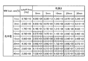
図9は、第1の実施形態における噴射孔の直径と、マイクロ波の漏洩率との関係のシミュレーション結果の一例を示す図である。図9において、「孔半径」は、噴射孔13−2の直径D2に対応する噴射孔13−2の半径を示している。また、「MW leak rate[%]」は、処理空間Sへ投入されたマイクロ波の強度に対する、噴射孔13−2へ漏れ込んだマイクロ波の強度の比率である漏洩率を示している。 FIG. 9 is a view showing an example of a simulation result of the relationship between the diameter of the injection hole and the leakage rate of the microwave in the first embodiment. In FIG. 9, "hole radius" indicates the radius of the injection hole 13-2 corresponding to the diameter D2 of the injection hole 13-2. Also, “MW leak rate [%]” indicates a leakage rate that is a ratio of the intensity of the microwaves leaking into the injection holes 13-2 to the intensity of the microwaves injected into the processing space S.
図9のシミュレーション結果から明らかなように、噴射孔13−2の直径D2を所定の上限値よりも小さくすることで、マイクロ波の漏洩率が、1%未満に改善される。ここで、所定の上限値とは、上記式(1)で決定される所定の上限値である。すなわち、噴射孔13−2の直径D2を、式(1)で決定される所定の上限値よりも小さくすることで、処理空間Sから噴射孔13−2へ漏れ込むマイクロ波の増大を抑制することが可能となることが分かった。 As apparent from the simulation result of FIG. 9, the microwave leakage rate is improved to less than 1% by making the diameter D2 of the injection holes 13-2 smaller than a predetermined upper limit value. Here, the predetermined upper limit value is a predetermined upper limit value determined by the equation (1). That is, by making the diameter D2 of the injection hole 13-2 smaller than the predetermined upper limit value determined by the equation (1), the increase of microwaves leaking from the processing space S to the injection hole 13-2 is suppressed. It turned out that it would be possible.
以上、第1の実施形態のプラズマ処理装置11によれば、輸送孔13−1によって処理容器12の側壁22の途中位置までガスを輸送し、輸送孔13−1よりも直径が大きい噴射孔13−2によって処理空間Sへガスを噴射する。その結果、第1の実施形態によれば、放電が発生し易い圧力の範囲以外の範囲までガスの圧力を低下させることができるので、圧力の増大に起因した放電を発生させることなくガスを導入することができる。
As described above, according to the
また、第1の実施形態のプラズマ処理装置11によれば、噴射孔13−2の直径を所定の上限値よりも小さくしているので、処理空間Sから噴射孔13−2へ漏れ込むマイクロ波の増大を抑制することができる。その結果、第1の実施形態によれば、噴射孔13−2又は噴射孔13−2の近傍の電界強度を低減することができるので、噴射孔13−2又は噴射孔13−2の近傍において放電が発生することを防止することができる。
Further, according to the
(第2の実施形態)
図10は、第2の実施形態におけるガス供給部、処理容器の側壁及び筒状誘電体の拡大断面図であり、図11は、図10に示したガス供給部、処理容器の側壁及び筒状誘電体を筒状誘電体の一端側から見た場合の正面図である。なお、以下に説明する点を除き、図10及び図11において、図5と同じ符号を付した構成は、図5における構成と同一又は同様の機能を有するため説明を省略する。
Second Embodiment
FIG. 10 is an enlarged sectional view of the gas supply unit, the side wall of the processing container, and the cylindrical dielectric in the second embodiment, and FIG. 11 is the gas supply unit shown in FIG. It is a front view at the time of seeing a dielectric from one end side of a cylindrical dielectric. 10 and FIG. 11, except for the points described below, have the same or similar functions as or to those of FIG.
図10及び図11に示すように、第2の実施形態に係るプラズマ処理装置は、一端61aが処理空間Sへ露出された状態で、噴射孔13−2の周囲を囲むように処理容器12の側壁22の側壁22に埋設された筒状誘電体61をさらに有する。筒状誘電体61は、アンテナ20によって処理空間Sへ放射されたマイクロ波を一端61aから、側壁22へ埋め込まれている他端61bへ導く。筒状誘電体61によって他端61bへ導かれたマイクロ波は、他端61bで反射し、反射前のマイクロ波と打ち消し合う。これにより、処理空間Sから噴射孔13−2へ漏れ込むマイクロ波の増大が抑制され、噴射孔13−2又は噴射孔13−2の近傍の電界強度が低減される。
As shown in FIGS. 10 and 11, in the plasma processing apparatus according to the second embodiment, with the one
筒状誘電体61の内部を伝播するマイクロ波の波長をλとすると、筒状誘電体61において一端61aから他端61bまでの長さは、λ/5以上3λ/5以下であることが好ましい。このように、筒状誘電体61において一端61aから他端61bまでの長さをλ/5以上3λ/5以下とすることによって、他端61bで反射したマイクロ波は、位相が反転されるので、誘電体に進入する前のマイクロ波を効率的に打ち消すことが可能となる。
Assuming that the wavelength of microwaves propagating inside the
図12は、第2の実施形態における筒状誘電体の有無に応じた噴射孔の電界強度のシミュレーション結果の一例を示す図である。図12に示したグラフにおいて、横軸は、処理空間Sの電子密度を示しており、縦軸は、筒状誘電体61が存在しない場合の噴射孔13−2の電界強度に対する、筒状誘電体61が埋設された場合の噴射孔13−2の電界強度の比を示している。
FIG. 12 is a view showing an example of a simulation result of the electric field strength of the injection hole according to the presence or absence of the cylindrical dielectric in the second embodiment. In the graph shown in FIG. 12, the horizontal axis shows the electron density in the processing space S, and the vertical axis shows the cylindrical dielectric relative to the electric field strength of the injection hole 13-2 when the
図12のシミュレーション結果から明らかなように、筒状誘電体61が埋設された場合、筒状誘電体61が存在しない場合と比較して、噴射孔13−2の電界強度を約70%だけ改善させることができた。
As apparent from the simulation result of FIG. 12, when the
以上、第2の実施形態のプラズマ処理装置によれば、処理容器12の側壁22の側壁22に噴射孔13−2の周囲を囲むように筒状誘電体61を埋設しているので、処理空間Sから噴射孔13−2へ漏れ込むマイクロ波の増大を抑制することができる。その結果、第2の実施形態によれば、噴射孔13−2又は噴射孔13−2の近傍の電界強度を低減することができるので、圧力の増大に起因した放電を発生させることなくガスを導入し、かつ、噴射孔13−2又は噴射孔13−2の近傍において放電が発生することをより効果的に防止することができる。
As described above, according to the plasma processing apparatus of the second embodiment, the
(第3の実施形態)
図13は、第3の実施形態におけるガス供給部、処理容器の側壁及び板状誘電体の拡大断面図である。なお、以下に説明する点を除き、図13において、図5と同じ符号を付した構成は、図5における構成と同一又は同様の機能を有するため説明を省略する。
Third Embodiment
FIG. 13 is an enlarged cross-sectional view of the gas supply unit, the side wall of the processing container, and the plate-like dielectric in the third embodiment. Note that, in FIG. 13, components denoted by the same reference numerals as in FIG. 5 have the same or similar functions as those in FIG.
図13に示すように、第3の実施形態に係るプラズマ処理装置は、一端71aが処理空間Sへ露出された状態で、処理容器12の側壁22のうち噴射孔13−2と誘電体部材16とに挟まれた領域に埋設された板状誘電体71をさらに有する。より具体的には、板状誘電体71は、処理容器12の側壁22のうち噴射孔13−2と誘電体部材16とに挟まれた領域に側壁22の周方向に沿って形成された凹部に、一端71aが処理空間Sへ露出された状態で、環状に埋め込まれている。板状誘電体71は、アンテナ20によって処理空間Sへ放射されたマイクロ波を一端71aから、側壁22へ埋め込まれている他端71bへ導く。板状誘電体71によって他端71bへ導かれたマイクロ波は、他端71bで反射し、反射前のマイクロ波と打ち消し合う。これにより、処理空間Sから噴射孔13−2へ漏れ込むマイクロ波の増大が抑制され、噴射孔13−2又は噴射孔13−2の近傍の電界強度が低減される。
As shown in FIG. 13, in the plasma processing apparatus according to the third embodiment, the injection holes 13-2 and the
板状誘電体71の内部を伝播するマイクロ波の波長をλとすると、板状誘電体71において一端71aから他端71bまでの長さは、λ/5以上3λ/5以下であることが好ましい。このように、板状誘電体71において一端71aから他端71bまでの長さをλ/5以上3λ/5以下とすることによって、他端71bで反射したマイクロ波は、位相が反転されるので、反射前のマイクロ波を効率的に打ち消すことが可能となる。
Assuming that the wavelength of microwaves propagating inside the plate-
以上、第3の実施形態のプラズマ処理装置によれば、処理容器12の側壁22のうち噴射孔13−2と誘電体部材16とに挟まれた領域に板状誘電体71を埋設しているので、処理空間Sから噴射孔13−2へ漏れ込むマイクロ波の増大を抑制することができる。その結果、第3の実施形態によれば、噴射孔13−2又は噴射孔13−2の近傍の電界強度を低減することができるので、圧力の増大に起因した放電を発生させることなくガスを導入し、かつ、噴射孔13−2又は噴射孔13−2の近傍において放電が発生することをより効果的に防止することができる。
As described above, according to the plasma processing apparatus of the third embodiment, the plate-
(第4の実施形態)
図14は、第4の実施形態におけるガス供給部、処理容器の側壁及び板状導電体の拡大断面図である。なお、以下に説明する点を除き、図14において、図5と同じ符号を付した構成は、図5における構成と同一又は同様の機能を有するため説明を省略する。
Fourth Embodiment
FIG. 14 is an enlarged cross-sectional view of the gas supply unit, the side wall of the processing container, and the plate-like conductor in the fourth embodiment. Note that, in FIG. 14, components denoted by the same reference numerals as in FIG. 5 have the same or similar functions as those in FIG.
図14に示すように、第4の実施形態に係るプラズマ処理装置は、処理容器12の側壁22のうち噴射孔13−2と誘電体部材16とに挟まれた領域から処理空間Sへ向けて突設された板状導電体81をさらに有する。より具体的には、板状導電体81は、処理容器12の側壁22のうち噴射孔13−2と誘電体部材16とに挟まれた領域から処理空間Sへ向けて環状に突設されている。板状導電体81は、アンテナ20によって処理空間Sへ放射されたマイクロ波を遮断する。これにより、処理空間Sから噴射孔13−2へ漏れ込むマイクロ波の増大が抑制され、噴射孔13−2又は噴射孔13−2の近傍の電界強度が低減される。
As shown in FIG. 14, in the plasma processing apparatus according to the fourth embodiment, a region of the
図15は、第3の実施形態における板状誘電体又は第4の実施形態における板状導電体の有無に応じた噴射孔の電界強度のシミュレーション結果の一例を示す図である。図15において、「STD」は、板状誘電体71及び板状導電体81のいずれも存在しない場合の噴射孔13−2の電界強度を示すグラフである。また、「Choke 2」は、板状誘電体71が埋設された場合の噴射孔13−2の電界強度を示すグラフである。また、「Metal Bar」は、板状導電体81が突設された場合の噴射孔13−2の電界強度を示すグラフである。また、図15に示した各グラフにおいて、横軸は、処理空間Sの電子密度を示しており、縦軸は、電界強度を示している。また、図15のシミュレーションでは、シミュレーション条件として、投入されるマイクロ波の電力:3kWが用いられたものとする。
FIG. 15 is a view showing an example of a simulation result of the electric field strength of the injection hole according to the presence or absence of the plate dielectric in the third embodiment or the plate conductor in the fourth embodiment. In FIG. 15, “STD” is a graph showing the electric field strength of the injection hole 13-2 when neither the plate-
図15のシミュレーション結果から明らかなように、板状誘電体71が埋設された場合、板状誘電体71及び板状導電体81のいずれも存在しない場合と比較して、噴射孔13−2の電界強度が低減された。
As apparent from the simulation result of FIG. 15, when the plate-
また、図15のシミュレーション結果から明らかなように、板状導電体81が突設された場合、板状誘電体71が埋設された場合と比較して、噴射孔13−2の電界強度が低減された。すなわち、板状導電体81を突設することによって、噴射孔13−2の電界強度を最も効率的に低減することができることが分かった。
Further, as apparent from the simulation result of FIG. 15, when the plate-like conductor 81 is provided in a protruding manner, the electric field strength of the injection hole 13-2 is reduced compared to the case where the plate-
以上、第4の実施形態のプラズマ処理装置によれば、処理容器12の側壁22のうち噴射孔13−2と誘電体部材16とに挟まれた領域から板状導電体81を突設しているので、処理空間Sから噴射孔13−2へ漏れ込むマイクロ波の増大を抑制することができる。その結果、第4の実施形態によれば、噴射孔13−2又は噴射孔13−2の近傍の電界強度を低減することができるので、圧力の増大に起因した放電を発生させることなくガスを導入し、かつ、噴射孔13−2又は噴射孔13−2の近傍において放電が発生することをより効果的に防止することができる。
As described above, according to the plasma processing apparatus of the fourth embodiment, the plate-like conductor 81 is provided so as to project from the region of the
なお、上記第1〜第4の実施形態では、噴射孔13−2の直径D2が一定である例を示したが、開示技術はこれには限定されない。例えば、噴射孔13−2の直径D2は、輸送孔13−1から遠ざかるほど、大きくなるようにしてもよい。これにより、噴射孔13−2からガスを円滑に噴射するとともに、放電が発生し易い圧力の範囲以外の範囲までガスの圧力を低下させることができるので、圧力の増大に起因した放電を発生させることなくガスを安定的に導入することができる。 In the first to fourth embodiments, the diameter D2 of the injection hole 13-2 is constant, but the disclosed technology is not limited to this. For example, the diameter D2 of the injection hole 13-2 may be made larger as it goes away from the transport hole 13-1. As a result, the gas can be smoothly injected from the injection holes 13-2 and the pressure of the gas can be reduced to a range other than the range of the pressure at which the discharge tends to occur. Therefore, the discharge due to the increase in pressure is generated. Gas can be introduced stably without
また、上記第2の実施形態では、筒状誘電体61は、輸送孔13−1に連通された噴射孔13−2の周囲を囲むように処理容器12の側壁22に埋設されるが、開示技術はこれには限定されない。例えば、輸送孔13−1と噴射孔13−2とを含む2段構造に代えて、1段の噴射孔のみが処理容器12の側壁22に形成される構造も採用され得る。このような構造では、筒状誘電体61は、1段の噴射孔の周囲を囲むように処理容器12の側壁22に埋設されてもよい。これにより、1段の噴射孔のみが処理容器12の側壁22に形成される構造が採用される場合であっても、圧力の増大に起因した放電を発生させることなくガスを導入することができる。
In the second embodiment, the
また、上記第3の実施形態では、板状誘電体71は、処理容器12の側壁22のうち輸送孔13−1に連通された噴射孔13−2と誘電体部材16とに挟まれた領域に埋設されるが、開示技術はこれには限定されない。例えば、輸送孔13−1と噴射孔13−2とを含む2段構造に代えて、1段の噴射孔のみが処理容器12の側壁22に形成される構造も採用され得る。このような構造では、板状誘電体71は、1段の噴射孔と誘電体部材16とに挟まれた領域に埋設されてもよい。これにより、1段の噴射孔のみが処理容器12の側壁22に形成される構造が採用される場合であっても、圧力の増大に起因した放電を発生させることなくガスを導入することができる。
In the third embodiment, the plate-
また、上記第4の実施形態では、板状導電体81は、処理容器12の側壁22のうち噴射孔13−2と誘電体部材16とに挟まれた領域から処理空間Sへ向けて突設されるが、開示技術はこれには限定されない。例えば、輸送孔13−1と噴射孔13−2とを含む2段構造に代えて、1段の噴射孔のみが処理容器12の側壁22に形成される構造も採用され得る。このような構造では、板状導電体81は、1段の噴射孔と誘電体部材16とに挟まれた領域から処理空間Sへ向けて突設されてもよい。これにより、1段の噴射孔のみが処理容器12の側壁22に形成される構造が採用される場合であっても、圧力の増大に起因した放電を発生させることなくガスを導入することができる。
In the fourth embodiment, the plate-like conductor 81 protrudes from the region of the
また、上記第2〜4の実施形態では、プラズマ処理装置は、筒状誘電体61、板状誘電体71又は板状導電体81を別個に備えるが、開示技術はこれには限られない。例えば、プラズマ処理装置は、筒状誘電体61、板状誘電体71及び板状導電体81のうち少なくともいずれか一つを備えていてもよい。
In the second to fourth embodiments, the plasma processing apparatus separately includes the
11 プラズマ処理装置
12 処理容器
13 ガス供給部
13−1 輸送孔
13−2 噴射孔
14 保持台
15 マイクロ波発生器
16 誘電体部材
16a 対向面
16b 面
17 スロット孔
18 スロットアンテナ板
19 遅波板
20 アンテナ
21 底部
22 側壁
23 排気孔
24 Oリング
26a 内周側スロット孔群
26b 外周側スロット孔群
27 遅波板突出部
28 中心
31 同軸導波管
32 内導体
33 外導体
34 隙間
35、38 端部
36 外周面
37 内周面
39 導波管
40 モード変換器
41 誘電体板押さえリング
42 アンテナ押さえ
43 冷却板
44 電磁遮蔽弾力体
45 外周固定リング
46 中心固定板
47 冷却板突出部
48 遅波板位置決め部
49 受け入れ凹部
50 内周面
51 スタブ部材
52 棒状部
53 ねじ部
54 ねじ孔
55 先端部
61 筒状誘電体
61a 一端
61b 他端
71 板状誘電体
71a 一端
71b 他端
81 板状導電体
11
Claims (8)
前記処理容器の側壁に設けられ、前記処理空間にガスを供給するガス供給部と、
前記処理空間に供給されるガスのプラズマを生成するプラズマ生成部と
を備え、
前記ガス供給部は、
前記処理容器の側壁の内部において前記処理空間へ到達しない位置まで前記ガスを輸送する輸送孔と、
前記輸送孔に連通され、前記位置まで輸送された前記ガスを前記処理空間へ噴射する噴射孔であって、前記輸送孔よりも直径が大きい噴射孔と
を有し、
前記噴射孔は、直径が略一定である内壁面を有することを特徴とするプラズマ処理装置。 A processing vessel defining a processing space;
A gas supply unit which is provided on a side wall of the processing container and supplies a gas to the processing space;
A plasma generation unit configured to generate a plasma of a gas supplied to the processing space;
The gas supply unit
A transport hole for transporting the gas to a position not reaching the processing space inside the side wall of the processing container;
It said communicating with the transport holes, the said gas is transported to a position a injection hole for injecting into the processing space, have a said transport injection hole even larger in diameter than the hole,
The plasma processing apparatus , wherein the injection hole has an inner wall surface having a substantially constant diameter .
前記処理空間に対向する対向面を有する誘電体部材と、
前記誘電体部材の前記対向面とは反対側の面上に設けられ、前記ガスをプラズマ化するマイクロ波を、前記誘電体部材を介して前記処理空間へ放射するアンテナと
を有することを特徴とする請求項1に記載のプラズマ処理装置。 The plasma generation unit is
A dielectric member having an opposing surface facing the processing space;
An antenna which is provided on the surface of the dielectric member opposite to the facing surface and radiates microwaves for plasmatizing the gas into the processing space through the dielectric member. The plasma processing apparatus according to claim 1 .
前記所定の上限値は、以下の式(1)を用いて、決定されることを特徴とする請求項1又は2に記載のプラズマ処理装置。
a<Pnm/(2πf(με)1/2) ・・・ (1)
ただし、
a:噴射孔の半径(所定の上限値/2)
Pnm:n次のベッセル関数Jn(P)が0となる複数の変数Pの解のうち、m番目に小さい変数Pの解(ただし、m、nは自然数)
f:マイクロ波の周波数
μ:前記噴射孔の内部における透磁率
ε:前記噴射孔の内部における誘電率 The diameter of the injection hole is smaller than a predetermined upper limit value,
The said predetermined upper limit is determined using the following formula | equation (1), The plasma processing apparatus of Claim 1 or 2 characterized by the above-mentioned.
a <P nm / (2πf (με) 1/2 ) (1)
However,
a: Radius of injection hole (predetermined upper limit / 2)
Pnm: n Bessel function Jn (P) is out of the solution of a plurality of variable P becomes 0, the solution of a small variable P to m-th (where, m, n are natural numbers)
f: microwave frequency μ: permeability in the inside of the injection hole ε: permittivity in the inside of the injection hole
前記処理容器の側壁に設けられ、前記処理空間にガスを供給するガス供給部と、
前記処理空間に供給されるガスのプラズマを生成するプラズマ生成部と
を備え、
前記ガス供給部は、
前記処理容器の側壁の内部において前記処理空間へ到達しない位置まで前記ガスを輸送する輸送孔と、
前記輸送孔に連通され、前記位置まで輸送された前記ガスを前記処理空間へ噴射する噴射孔であって、前記輸送孔よりも直径が大きい噴射孔と
を有し、
前記プラズマ生成部は、
前記処理空間に対向する対向面を有する誘電体部材と、
前記誘電体部材の前記対向面とは反対側の面上に設けられ、前記ガスをプラズマ化するマイクロ波を、前記誘電体部材を介して前記処理空間へ放射するアンテナと
を有し、
一端が前記処理空間へ露出された状態で、前記噴射孔の周囲を囲むように前記処理容器の側壁に埋設され、前記アンテナによって前記処理空間へ放射された前記マイクロ波を前記一端から他端へ導く筒状誘電体をさらに備えることを特徴とするプラズマ処理装置。 A processing vessel defining a processing space;
A gas supply unit which is provided on a side wall of the processing container and supplies a gas to the processing space;
A plasma generation unit for generating plasma of a gas supplied to the processing space;
Equipped with
The gas supply unit
A transport hole for transporting the gas to a position not reaching the processing space inside the side wall of the processing container;
An injection hole communicated with the transport hole and injecting the gas transported to the position into the processing space, the injection hole having a diameter larger than the transport hole, and
Have
The plasma generation unit is
A dielectric member having an opposing surface facing the processing space;
An antenna which is provided on the surface of the dielectric member opposite to the opposite surface, and which radiates microwaves for plasmatizing the gas into the processing space through the dielectric member;
Have
One end is embedded in a side wall of the processing container so as to surround the injection hole in a state of being exposed to the processing space, and the microwave radiated to the processing space by the antenna is transmitted from the one end to the other end features and to pulp plasma processing apparatus further comprising a cylindrical dielectric guiding.
前記処理容器の側壁に設けられ、前記処理空間にガスを供給するガス供給部と、
前記処理空間に供給されるガスのプラズマを生成するプラズマ生成部と
を備え、
前記ガス供給部は、
前記処理容器の側壁の内部において前記処理空間へ到達しない位置まで前記ガスを輸送する輸送孔と、
前記輸送孔に連通され、前記位置まで輸送された前記ガスを前記処理空間へ噴射する噴射孔であって、前記輸送孔よりも直径が大きい噴射孔と
を有し、
前記プラズマ生成部は、
前記処理空間に対向する対向面を有する誘電体部材と、
前記誘電体部材の前記対向面とは反対側の面上に設けられ、前記ガスをプラズマ化するマイクロ波を、前記誘電体部材を介して前記処理空間へ放射するアンテナと
を有し、
一端が前記処理空間へ露出された状態で、前記処理容器の側壁のうち前記噴射孔と前記誘電体部材とに挟まれた領域に埋設され、前記アンテナによって前記処理空間へ放射された前記マイクロ波を前記一端から他端へ導く板状誘電体をさらに備えることを特徴とするプラズマ処理装置。 A processing vessel defining a processing space;
A gas supply unit which is provided on a side wall of the processing container and supplies a gas to the processing space;
A plasma generation unit for generating plasma of a gas supplied to the processing space;
Equipped with
The gas supply unit
A transport hole for transporting the gas to a position not reaching the processing space inside the side wall of the processing container;
An injection hole communicated with the transport hole and injecting the gas transported to the position into the processing space, the injection hole having a diameter larger than the transport hole, and
Have
The plasma generation unit is
A dielectric member having an opposing surface facing the processing space;
An antenna which is provided on the surface of the dielectric member opposite to the opposite surface, and which radiates microwaves for plasmatizing the gas into the processing space through the dielectric member;
Have
The microwave which is embedded in a region of the side wall of the processing container sandwiched between the injection hole and the dielectric member in a state where one end is exposed to the processing space, and the microwave radiated to the processing space by the antenna it further comprises a plate-like dielectric which leads to the other end from the one end features and to pulp plasma processing apparatus.
前記筒状誘電体において前記一端から前記他端までの長さは、λ/5以上3λ/5以下であることを特徴とする請求項4に記載のプラズマ処理装置。 Assuming that the wavelength of the microwave propagating inside the cylindrical dielectric is λ,
5. The plasma processing apparatus according to claim 4 , wherein the length from the one end to the other end of the cylindrical dielectric is λ / 5 or more and 3λ / 5 or less.
前記板状誘電体において前記一端から前記他端までの長さは、λ/5以上3λ/5以下であることを特徴とする請求項5に記載のプラズマ処理装置。 Assuming that the wavelength of the microwave propagating inside the plate dielectric is λ,
The plasma processing apparatus according to claim 5 , wherein a length from the one end to the other end of the plate-like dielectric is λ / 5 or more and 3λ / 5 or less.
前記処理容器の側壁に設けられ、前記処理空間にガスを供給するガス供給部と、
前記処理空間に供給されるガスのプラズマを生成するプラズマ生成部と
を備え、
前記ガス供給部は、
前記処理容器の側壁の内部において前記処理空間へ到達しない位置まで前記ガスを輸送する輸送孔と、
前記輸送孔に連通され、前記位置まで輸送された前記ガスを前記処理空間へ噴射する噴射孔であって、前記輸送孔よりも直径が大きい噴射孔と
を有し、
前記プラズマ生成部は、
前記処理空間に対向する対向面を有する誘電体部材と、
前記誘電体部材の前記対向面とは反対側の面上に設けられ、前記ガスをプラズマ化するマイクロ波を、前記誘電体部材を介して前記処理空間へ放射するアンテナと
を有し、
前記処理容器の側壁のうち前記噴射孔と前記誘電体部材とに挟まれた領域から前記処理空間へ向けて突設され、前記アンテナによって前記処理空間へ放射された前記マイクロ波を遮断する板状導電体をさらに備えることを特徴とするプラズマ処理装置。 A processing vessel defining a processing space;
A gas supply unit which is provided on a side wall of the processing container and supplies a gas to the processing space;
A plasma generation unit for generating plasma of a gas supplied to the processing space;
Equipped with
The gas supply unit
A transport hole for transporting the gas to a position not reaching the processing space inside the side wall of the processing container;
An injection hole communicated with the transport hole and injecting the gas transported to the position into the processing space, the injection hole having a diameter larger than the transport hole, and
Have
The plasma generation unit is
A dielectric member having an opposing surface facing the processing space;
An antenna which is provided on the surface of the dielectric member opposite to the opposite surface, and which radiates microwaves for plasmatizing the gas into the processing space through the dielectric member;
Have
A plate-like shape projecting toward the processing space from a region of the side wall of the processing vessel sandwiched between the injection hole and the dielectric member and blocking the microwaves radiated to the processing space by the antenna features and to pulp plasma processing apparatus further comprises a conductor.
Priority Applications (4)
| Application Number | Priority Date | Filing Date | Title |
|---|---|---|---|
| JP2014225390A JP6501493B2 (en) | 2014-11-05 | 2014-11-05 | Plasma processing system |
| KR1020150154429A KR102426265B1 (en) | 2014-11-05 | 2015-11-04 | Plasma processing apparatus |
| US14/931,919 US10566174B2 (en) | 2014-11-05 | 2015-11-04 | Plasma processing apparatus |
| US16/752,153 US11456157B2 (en) | 2014-11-05 | 2020-01-24 | Plasma processing apparatus |
Applications Claiming Priority (1)
| Application Number | Priority Date | Filing Date | Title |
|---|---|---|---|
| JP2014225390A JP6501493B2 (en) | 2014-11-05 | 2014-11-05 | Plasma processing system |
Publications (3)
| Publication Number | Publication Date |
|---|---|
| JP2016091821A JP2016091821A (en) | 2016-05-23 |
| JP2016091821A5 JP2016091821A5 (en) | 2017-12-07 |
| JP6501493B2 true JP6501493B2 (en) | 2019-04-17 |
Family
ID=55853449
Family Applications (1)
| Application Number | Title | Priority Date | Filing Date |
|---|---|---|---|
| JP2014225390A Active JP6501493B2 (en) | 2014-11-05 | 2014-11-05 | Plasma processing system |
Country Status (3)
| Country | Link |
|---|---|
| US (2) | US10566174B2 (en) |
| JP (1) | JP6501493B2 (en) |
| KR (1) | KR102426265B1 (en) |
Families Citing this family (5)
| Publication number | Priority date | Publication date | Assignee | Title |
|---|---|---|---|---|
| JP6850636B2 (en) * | 2017-03-03 | 2021-03-31 | 東京エレクトロン株式会社 | Plasma processing equipment |
| JP7058485B2 (en) * | 2017-05-16 | 2022-04-22 | 東京エレクトロン株式会社 | Plasma processing equipment |
| CN108878248B (en) * | 2017-05-16 | 2020-03-17 | 东京毅力科创株式会社 | Plasma processing apparatus |
| CN107731649B (en) * | 2017-10-23 | 2018-06-08 | 北京大学 | A kind of device of multifunctional semiconductor doping |
| JP2021064508A (en) * | 2019-10-11 | 2021-04-22 | 東京エレクトロン株式会社 | Plasma processing apparatus |
Family Cites Families (28)
| Publication number | Priority date | Publication date | Assignee | Title |
|---|---|---|---|---|
| JPS53118557A (en) | 1977-03-22 | 1978-10-17 | Fujimoto Seiyaku Kk | Production of garlic extract having ascorbic acid staibilizing property |
| US4854263B1 (en) * | 1987-08-14 | 1997-06-17 | Applied Materials Inc | Inlet manifold and methods for increasing gas dissociation and for PECVD of dielectric films |
| US5134965A (en) * | 1989-06-16 | 1992-08-04 | Hitachi, Ltd. | Processing apparatus and method for plasma processing |
| US5824605A (en) * | 1995-07-31 | 1998-10-20 | Lam Research Corporation | Gas dispersion window for plasma apparatus and method of use thereof |
| JP3155199B2 (en) * | 1996-04-12 | 2001-04-09 | 東京エレクトロン株式会社 | Plasma processing equipment |
| US7196283B2 (en) * | 2000-03-17 | 2007-03-27 | Applied Materials, Inc. | Plasma reactor overhead source power electrode with low arcing tendency, cylindrical gas outlets and shaped surface |
| EP1398826A4 (en) * | 2001-06-20 | 2006-09-06 | Tadahiro Ohmi | Microwave plasma processing device, plasma processing method, and microwave radiating member |
| JP3969081B2 (en) * | 2001-12-14 | 2007-08-29 | 東京エレクトロン株式会社 | Plasma processing equipment |
| JP4062928B2 (en) * | 2002-02-06 | 2008-03-19 | 東京エレクトロン株式会社 | Plasma processing equipment |
| KR101153161B1 (en) * | 2005-04-01 | 2012-06-18 | 주성엔지니어링(주) | Gas injector and Apparatus including the same for fabricating Liquid Crystal Display Device |
| US20080254220A1 (en) * | 2006-01-20 | 2008-10-16 | Tokyo Electron Limited | Plasma processing apparatus |
| KR100978407B1 (en) * | 2006-03-06 | 2010-08-26 | 도쿄엘렉트론가부시키가이샤 | Plasma processing apparatus |
| WO2008123060A1 (en) * | 2007-03-28 | 2008-10-16 | Canon Anelva Corporation | Vacuum processing apparatus |
| JP5058727B2 (en) * | 2007-09-06 | 2012-10-24 | 東京エレクトロン株式会社 | Top plate structure and plasma processing apparatus using the same |
| JP4590597B2 (en) * | 2008-03-12 | 2010-12-01 | 国立大学法人東北大学 | Shower plate manufacturing method |
| JP2010074065A (en) * | 2008-09-22 | 2010-04-02 | Canon Anelva Corp | Substrate cleaning method for removing oxide film |
| JP5357486B2 (en) * | 2008-09-30 | 2013-12-04 | 東京エレクトロン株式会社 | Plasma processing equipment |
| JP2010118549A (en) * | 2008-11-13 | 2010-05-27 | Tokyo Electron Ltd | Plasma etching method and plasma etching device |
| WO2010073578A1 (en) * | 2008-12-24 | 2010-07-01 | 芝浦メカトロニクス株式会社 | Plasma generating apparatus and plasma processing apparatus |
| JP2010212277A (en) * | 2009-03-06 | 2010-09-24 | Sharp Corp | Film forming apparatus |
| KR101378304B1 (en) * | 2009-08-21 | 2014-03-27 | 도쿄엘렉트론가부시키가이샤 | Plasma processing apparatus and substrate processing method |
| JP5457109B2 (en) * | 2009-09-02 | 2014-04-02 | 東京エレクトロン株式会社 | Plasma processing equipment |
| KR101612741B1 (en) * | 2010-03-08 | 2016-04-18 | 주성엔지니어링(주) | Gas distributing plate and Apparatus for treating substrate including the same |
| JP5835985B2 (en) * | 2010-09-16 | 2015-12-24 | 東京エレクトロン株式会社 | Plasma processing apparatus and plasma processing method |
| US20120180954A1 (en) * | 2011-01-18 | 2012-07-19 | Applied Materials, Inc. | Semiconductor processing system and methods using capacitively coupled plasma |
| JP5955062B2 (en) * | 2011-04-25 | 2016-07-20 | 東京エレクトロン株式会社 | Plasma processing equipment |
| JP2014082354A (en) * | 2012-10-17 | 2014-05-08 | Hitachi High-Technologies Corp | Plasma processing apparatus |
| KR20160002543A (en) * | 2014-06-30 | 2016-01-08 | 세메스 주식회사 | Substrate treating apparatus |
-
2014
- 2014-11-05 JP JP2014225390A patent/JP6501493B2/en active Active
-
2015
- 2015-11-04 US US14/931,919 patent/US10566174B2/en active Active
- 2015-11-04 KR KR1020150154429A patent/KR102426265B1/en active IP Right Grant
-
2020
- 2020-01-24 US US16/752,153 patent/US11456157B2/en active Active
Also Published As
| Publication number | Publication date |
|---|---|
| US20200161090A1 (en) | 2020-05-21 |
| JP2016091821A (en) | 2016-05-23 |
| US11456157B2 (en) | 2022-09-27 |
| KR102426265B1 (en) | 2022-07-29 |
| US20160126066A1 (en) | 2016-05-05 |
| KR20160053816A (en) | 2016-05-13 |
| US10566174B2 (en) | 2020-02-18 |
Similar Documents
| Publication | Publication Date | Title |
|---|---|---|
| TWI719290B (en) | Plasma processing tool using modular microwave sources | |
| US11456157B2 (en) | Plasma processing apparatus | |
| TWI681073B (en) | Plasma treatment device | |
| JP5717888B2 (en) | Plasma processing equipment | |
| JP5082229B2 (en) | Plasma processing equipment | |
| KR101751200B1 (en) | Microwave radiation antenna, microwave plasma source and plasma processing apparatus | |
| JP5243457B2 (en) | Top plate of microwave plasma processing apparatus, plasma processing apparatus and plasma processing method | |
| TW202410131A (en) | Processing tool for remote modular high-frequency source | |
| JP2020009746A (en) | Phased array module type high frequency source | |
| KR101882608B1 (en) | Plasma processing apparatus and plasma processing method | |
| WO2016104205A1 (en) | Plasma processing device and plasma processing method | |
| JP2007035411A (en) | Plasma treatment device | |
| TWI839354B (en) | Modular high-frequency source | |
| KR102131539B1 (en) | Microwave plasma processing apparatus | |
| JP2016091603A (en) | Microwave plasma processing device | |
| TWI587751B (en) | Microwave radiation antenna, microwave plasma source and plasma processing device | |
| JP6700128B2 (en) | Microwave plasma processing equipment | |
| JP2022039821A (en) | Plasma processing device, plasma processing method, and dielectric window | |
| KR20210104756A (en) | Plasma treatment apparatus and plasma treatment method | |
| JP5667368B2 (en) | Plasma processing equipment | |
| JP2018006256A (en) | Microwave plasma processing device | |
| TW202431906A (en) | Modular high-frequency source | |
| KR20230026265A (en) | Plasma processing apparatus and lid member | |
| US20160358756A1 (en) | Plasma processing apparatus | |
| KR20160062699A (en) | Plasma processing device |
Legal Events
| Date | Code | Title | Description |
|---|---|---|---|
| A521 | Request for written amendment filed |
Free format text: JAPANESE INTERMEDIATE CODE: A523 Effective date: 20171027 |
|
| A621 | Written request for application examination |
Free format text: JAPANESE INTERMEDIATE CODE: A621 Effective date: 20171027 |
|
| A977 | Report on retrieval |
Free format text: JAPANESE INTERMEDIATE CODE: A971007 Effective date: 20180822 |
|
| A131 | Notification of reasons for refusal |
Free format text: JAPANESE INTERMEDIATE CODE: A131 Effective date: 20180904 |
|
| A521 | Request for written amendment filed |
Free format text: JAPANESE INTERMEDIATE CODE: A523 Effective date: 20181029 |
|
| TRDD | Decision of grant or rejection written | ||
| A01 | Written decision to grant a patent or to grant a registration (utility model) |
Free format text: JAPANESE INTERMEDIATE CODE: A01 Effective date: 20190219 |
|
| A61 | First payment of annual fees (during grant procedure) |
Free format text: JAPANESE INTERMEDIATE CODE: A61 Effective date: 20190319 |
|
| R150 | Certificate of patent or registration of utility model |
Ref document number: 6501493 Country of ref document: JP Free format text: JAPANESE INTERMEDIATE CODE: R150 |
|
| R250 | Receipt of annual fees |
Free format text: JAPANESE INTERMEDIATE CODE: R250 |
|
| R250 | Receipt of annual fees |
Free format text: JAPANESE INTERMEDIATE CODE: R250 |
|
| R250 | Receipt of annual fees |
Free format text: JAPANESE INTERMEDIATE CODE: R250 |