JP4702425B2 - Signal transmitting apparatus and signal transmitting method - Google Patents
Signal transmitting apparatus and signal transmitting method Download PDFInfo
- Publication number
- JP4702425B2 JP4702425B2 JP2008263243A JP2008263243A JP4702425B2 JP 4702425 B2 JP4702425 B2 JP 4702425B2 JP 2008263243 A JP2008263243 A JP 2008263243A JP 2008263243 A JP2008263243 A JP 2008263243A JP 4702425 B2 JP4702425 B2 JP 4702425B2
- Authority
- JP
- Japan
- Prior art keywords
- data
- reference signal
- bits
- timing reference
- bit
- Prior art date
- Legal status (The legal status is an assumption and is not a legal conclusion. Google has not performed a legal analysis and makes no representation as to the accuracy of the status listed.)
- Active
Links
Images


Classifications
-
- H—ELECTRICITY
- H04—ELECTRIC COMMUNICATION TECHNIQUE
- H04N—PICTORIAL COMMUNICATION, e.g. TELEVISION
- H04N5/00—Details of television systems
- H04N5/222—Studio circuitry; Studio devices; Studio equipment
- H04N5/262—Studio circuits, e.g. for mixing, switching-over, change of character of image, other special effects ; Cameras specially adapted for the electronic generation of special effects
- H04N5/268—Signal distribution or switching
-
- H—ELECTRICITY
- H04—ELECTRIC COMMUNICATION TECHNIQUE
- H04N—PICTORIAL COMMUNICATION, e.g. TELEVISION
- H04N21/00—Selective content distribution, e.g. interactive television or video on demand [VOD]
- H04N21/20—Servers specifically adapted for the distribution of content, e.g. VOD servers; Operations thereof
- H04N21/23—Processing of content or additional data; Elementary server operations; Server middleware
- H04N21/236—Assembling of a multiplex stream, e.g. transport stream, by combining a video stream with other content or additional data, e.g. inserting a URL [Uniform Resource Locator] into a video stream, multiplexing software data into a video stream; Remultiplexing of multiplex streams; Insertion of stuffing bits into the multiplex stream, e.g. to obtain a constant bit-rate; Assembling of a packetised elementary stream
- H04N21/23602—Multiplexing isochronously with the video sync, e.g. according to bit-parallel or bit-serial interface formats, as SDI
-
- H—ELECTRICITY
- H04—ELECTRIC COMMUNICATION TECHNIQUE
- H04N—PICTORIAL COMMUNICATION, e.g. TELEVISION
- H04N21/00—Selective content distribution, e.g. interactive television or video on demand [VOD]
- H04N21/40—Client devices specifically adapted for the reception of or interaction with content, e.g. set-top-box [STB]; Operations thereof
- H04N21/43—Processing of content or additional data, e.g. demultiplexing additional data from a digital video stream; Elementary client operations, e.g. monitoring of home network or synchronising decoder's clock; Client middleware
- H04N21/434—Disassembling of a multiplex stream, e.g. demultiplexing audio and video streams, extraction of additional data from a video stream; Remultiplexing of multiplex streams; Extraction or processing of SI; Disassembling of packetised elementary stream
- H04N21/4342—Demultiplexing isochronously with video sync, e.g. according to bit-parallel or bit-serial interface formats, as SDI
-
- H—ELECTRICITY
- H04—ELECTRIC COMMUNICATION TECHNIQUE
- H04N—PICTORIAL COMMUNICATION, e.g. TELEVISION
- H04N7/00—Television systems
- H04N7/015—High-definition television systems
-
- H—ELECTRICITY
- H04—ELECTRIC COMMUNICATION TECHNIQUE
- H04N—PICTORIAL COMMUNICATION, e.g. TELEVISION
- H04N7/00—Television systems
- H04N7/12—Systems in which the television signal is transmitted via one channel or a plurality of parallel channels, the bandwidth of each channel being less than the bandwidth of the television signal
Abstract
Description
本発明は、例えば、3840×2160/24P,24/1.001P,25P,30P,30/1.001P/4:4:4/12ビット信号をビットレート10Gbps以上でシリアル伝送する場合に適用して好適な信号送信装置及び信号送信方法に関する。 The present invention is applied to, for example, 3840 × 2160 / 24P, 24 / 1.001P, 25P, 30P, 30 / 1.001P / 4: 4: 4 / 12-bit signal serially transmitted at a bit rate of 10 Gbps or more. In particular, the present invention relates to a signal transmission apparatus and a signal transmission method.
本出願人は、3840×2160/24P,24/1.001P,25P,30P,30/1.001P/4:4:4/12ビット信号を、ビットレート10Gbps以上でシリアル伝送する技術を既に開示済みである。3840×2160/24P,24/1.001P,25P,30P,30/1.001P/4:4:4/12ビット信号は、4k×2k信号(4kサンプル×2kラインの超高解像度信号)の一種である。
ところで、特許文献1に開示された技術を用いて、4k×2k信号のシリアル伝送を行う場合、単一色のみからなる画面(フラットフィールド)を構成する映像信号の生成が行えなくなることが判明した。この点について図20を参照して説明する。
By the way, it has been found that when the 4k × 2k signal is serially transmitted using the technique disclosed in
図20は、従来のベーシックストリームの伝送例を示す。
図20Aは、ベーシックストリームCH1,3,5,7を伝送する場合におけるデータ構造の例を示す。
従来、ベーシックストリームCH1,3,5,7のEAVに続くフィールド101には、(LN0,LN0,LN1,LN1)が含まれる。CH1,3,5,7のSAV内における(3FFh,3FFh,000h,000h,000h,000h,XYZ,ZYZh)のフィールド102で示される(000h,000h,000h,000h)はそのままスクランブルが掛けられる。このとき、CXYZhの下位2ビットを、CH1,3,5,7でそれぞれ、(0,0),(0,1),(1,0),(1,1)に書き換える。
FIG. 20 shows an example of transmission of a conventional basic stream.
FIG. 20A shows an example of a data structure when basic streams CH1, 3, 5, and 7 are transmitted.
Conventionally, the
図20Bは、ベーシックストリームCH2,4,6,8を伝送する場合におけるデータ構造の例を示す。
ベーシックストリームCH2,4,6,8は、それぞれSAVとアクティブビデオとEAVによって構成される映像信号に変換される。ただし、この映像信号は、8B/10B変換される。
FIG. 20B shows an example of the data structure when basic streams CH2, 4, 6, and 8 are transmitted.
The basic streams CH2, 4, 6, and 8 are converted into video signals each composed of SAV, active video, and EAV. However, this video signal is 8B / 10B converted.
図20Cは、10ビット8ワードのデータ構造の例を示す。
図20Aにおけるフィールド103と、図20Bにおけるフィールド104は、それぞれ、10ビット8ワードのデータに挿入される。
FIG. 20C shows an example of a data structure of 10 bits and 8 words.
The
ここで、フィールド103は元データをスクランブルしたデータであるため、K28.5信号に相当する8B/10B符号のワード同期信号を誤って生成することがある。例えば、単一色の映像信号をスクランブルした場合に、K28.5信号に相当する8B/10B符号のワード同期信号を生成すると、この8B/10B符号のワード同期信号が1フィールドの同じ水平位置に出力されてしまう。映像信号の出力は、ステートマシンによって制御されており、この8B/10B符号のワード同期信号が1フィールドの同じ水平位置に連続して出力されると、映像信号の出力のワード区切りを誤ってしまい、フラットフィールドの映像信号を出力できなくなる。
Here, since the
本発明はこのような状況に鑑みて成されたものであり、フラットフィールドの映像信号を好適に出力することを目的とする。 The present invention has been made in view of such a situation, and an object thereof is to suitably output a flat field video signal.
上記課題を解決するために、本発明は、所定の伝送規格に従ってマッピングされたCH1〜CH8のHD−SDIフォーマットのシリアル・デジタルビデオ信号を、それぞれシリアル/パラレル変換する。ここで、CH1〜CH8は、LinkAであるCH1,CH3,CH5,CH7及びLinkBであるCH2,CH4,CH6,CH8である。
次に、シリアル/パラレル変換されたLinkAの各水平ラインのデータのうち、000h,000h,000h,000hで規定されるタイミング基準信号SAVを所定の値に書き換え、タイミング基準信号SAV内の最後のワードであるXYZの下位2ビットをチャンネル毎に変える。
次に、スクランブラによって、タイミング基準信号SAV,アクティブライン,タイミング基準信号EAV,ライン番号LN及び誤り検出符号CRCのデータのみに自己同期型スクランブルを掛ける。
次に、タイミング基準信号SAVの直前でスクランブラ内のレジスタの値を全て0にセットしてエンコードし、誤り検出符号CRCに続く少なくとも数ビットまでのデータを出力する。
次に、シリアル/パラレル変換されたLinkBの各水平ラインのデータのうち、タイミング基準信号SAV,アクティブライン,タイミング基準信号EAV,ライン番号LN及び誤り検出符号CRCのデータのみからRGBのビットを抜き出す。
次に、抜き出されたLinkBのRGBのビットを8ビット/10ビットエンコーディングする。
次に、自己同期型スクランブルを掛けられたLinkAのパラレル・デジタルデータと、8ビット/10ビットエンコーディングされたLinkBのパラレル・デジタルデータとを多重する。
そして、多重されたパラレル・デジタルデータから、所定のビットレートのシリアル・デジタルデータを生成する。
In order to solve the above-described problems, the present invention serial / parallel converts serial digital video signals of CH1 to CH8 HD-SDI format mapped according to a predetermined transmission standard. Here, CH1 to CH8 are CH1, CH3, CH5, and CH7 that are LinkA, and CH2, CH4, CH6, and CH8 that are LinkB.
Next, the timing reference signal SAV defined by 000h, 000h, 000h, 000h is rewritten to a predetermined value in the serial / parallel converted data of each horizontal line of Link A, and the last word in the timing reference signal SAV is rewritten . the lower 2 bits of the XYZ Ru changed for each channel is.
Next, self-synchronous scrambling is applied only to the data of the timing reference signal SAV, the active line, the timing reference signal EAV, the line number LN, and the error detection code CRC by the scrambler.
Next, all the register values in the scrambler are set to 0 and encoded immediately before the timing reference signal SAV, and data up to at least several bits following the error detection code CRC is output.
Next, RGB bits are extracted from only the data of the timing reference signal SAV, the active line, the timing reference signal EAV, the line number LN, and the error detection code CRC from the serial / parallel converted data of each horizontal line of LinkB.
Next, the extracted LinkB RGB bits are subjected to 8-bit / 10-bit encoding.
Next, the link A parallel digital data subjected to self-synchronization scrambling and the link B parallel digital data encoded by 8 bits / 10 bits are multiplexed.
Then, serial digital data having a predetermined bit rate is generated from the multiplexed parallel digital data.
これにより、伝送規格に従ってマッピングされたCH1〜CH8のHD−SDIフォーマットのシリアル・デジタルビデオ信号を、それぞれシリアル/パラレル変換する。LinkAについては、タイミング基準信号SAV,アクティブライン,タイミング基準信号EAV,ライン番号LN及び誤り検出符号CRCのデータのみに自己同期型スクランブルを掛ける。一方、水平ブランキング期間のデータには自己同期型スクランブルを掛けない。そして、タイミング基準信号SAVの直前でスクランブラ内のレジスタの値を全て0にセットしてエンコードし、誤り検出符号CRCに続く少なくとも数ビットまでのデータを出力する。 As a result, the serial digital video signals in the HD-SDI format of CH1 to CH8 mapped according to the transmission standard are respectively converted into serial / parallel. For Link A, only the data of the timing reference signal SAV, the active line, the timing reference signal EAV, the line number LN, and the error detection code CRC are subjected to self-synchronization scrambling. On the other hand, self-synchronous scrambling is not applied to data in the horizontal blanking period. Then, immediately before the timing reference signal SAV, all the register values in the scrambler are set to 0 and encoded, and data of at least several bits following the error detection code CRC is output.
LinkBについては、各水平ラインのデータのうち、タイミング基準信号SAV,アクティブライン,タイミング基準信号EAV,ライン番号LN及び誤り検出符号CRCのデータのみからRGBのビットが抜き出される。このRGBのビットが8ビット/10ビットエンコーディングされる。そして、自己同期型スクランブルを掛けられたLinkAのデータと、8ビット/10ビットエンコーディングされたLinkBのデータとが多重される。その多重されたパラレル・デジタルデータから、所定のビットレートのシリアル・デジタルデータが生成される。 For Link B, RGB bits are extracted from only the data of the timing reference signal SAV, the active line, the timing reference signal EAV, the line number LN, and the error detection code CRC among the data of each horizontal line. The RGB bits are 8 bits / 10 bits encoded. Then, Link A data subjected to self-synchronization scrambling and Link B data encoded with 8 bits / 10 bits are multiplexed. Serial digital data having a predetermined bit rate is generated from the multiplexed parallel digital data.
本発明によれば、シリアル/パラレル変換されたLinkAの各水平ラインのデータのうち、000h,000h,000h,000hで規定されるタイミング基準信号SAVを所定の値に書き換える。このデータがスクランブルされた結果、フラットフィールドの映像信号であっても、タイミング基準信号SAVの値は異なる値となる。このため、あるデータがスクランブルされたことによって8B/10B符号のワード同期信号を示すデータに変換されたとしても、この8B/10B符号のワード同期信号を示すデータは連続しない。これにより、フィールドの映像信号を好適に出力できるという効果がある。 According to the present invention, the timing reference signal SAV defined by 000h, 000h, 000h, 000h is rewritten to a predetermined value in the data of each horizontal line of Link A subjected to serial / parallel conversion. As a result of this data being scrambled, the value of the timing reference signal SAV becomes a different value even for a flat field video signal. For this reason, even if certain data is scrambled and converted to data indicating the word synchronization signal of the 8B / 10B code, the data indicating the word synchronization signal of the 8B / 10B code is not continuous. Thereby, there is an effect that the video signal of the field can be suitably output.
以下、発明を実施するための最良の形態(以下実施の形態とする。)について説明する。なお、説明は以下の順序で行う。
1.第1の実施の形態(スクランブル制御:SAVへのデータ書換え処理の例)
2.変形例
Hereinafter, the best mode for carrying out the invention (hereinafter referred to as an embodiment) will be described. The description will be given in the following order.
1. First embodiment (scramble control: example of data rewriting process to SAV)
2. Modified example
<1.第1の実施の形態>
[伝送システムの例]
図1は、本発明を適用したテレビジョン放送局用のカメラ伝送システムの全体構成を示す図である。このカメラ伝送システムは、複数台の放送用カメラ1とCCU(カメラコントロールユニット)2とで構成されており各放送用カメラ1が光ファイバーケーブル3でCCU2に接続されている。
<1. First Embodiment>
[Example of transmission system]
FIG. 1 is a diagram showing an overall configuration of a camera transmission system for a television broadcasting station to which the present invention is applied. This camera transmission system includes a plurality of
各放送用カメラ1は、同一構成のものであり、3840×2160/24P,24/1.001P,25P,30P,30/1.001P(以下単に24P,25P,30Pと記載する)/4:4:4/12ビット信号を生成するカメラである。この信号は、4k×2k信号(4kサンプル×2kラインの超高解像度信号)として用いられる。
Each
CCU2は、各放送用カメラ1を制御したり、各放送用カメラ1から映像信号を受信したり、各放送用カメラ1のモニタに他の放送用カメラ1で撮影中の映像を表示させるための映像信号(リターンビデオ)送信するユニットである。
The CCU 2 controls each
[放送用カメラの内部構成例]
図2は、放送用カメラ1の回路構成のうち、本発明に関連する部分を示すブロック図である。放送用カメラ1内の撮像部及び映像信号処理部(図示略)によって生成された3840×2160/24P,25P,30P/4:4:4/12ビット信号が、マッピング部11に送られる。
[Broadcast camera internal configuration example]
FIG. 2 is a block diagram showing a part related to the present invention in the circuit configuration of the
図3は、この3840×2160/24P,25P,30P/4:4:4/12ビット信号のフォーマットを示す図である。3840×2160/24P,25P,30P/4:4:4/12ビット信号は、ワード長が12ビットずつのGデータ系列,Bデータ系列,Rデータ系列の同期を取って並列配置した、36ビット幅の信号である。1フレーム期間は1/24秒,1/25秒,1/30秒のうちのいずれかであり、1フレーム期間内に2160の有効ライン期間が含まれている。 FIG. 3 is a diagram showing the format of this 3840 × 2160 / 24P, 25P, 30P / 4: 4: 4 / 12-bit signal. 3840 × 2160 / 24P, 25P, 30P / 4: 4: 4 / 12-bit signals are arranged in parallel by synchronizing the G data series, B data series, and R data series each having a word length of 12 bits. It is a width signal. One frame period is any one of 1/24 seconds, 1/25 seconds, and 1/30 seconds, and 2160 effective line periods are included in one frame period.
各有効ライン期間には、タイミング基準信号EAV(End of Active Video)と、ライン番号LNと、誤り検出符号CRCが配置される。また、水平ブランキング期間(補助データ/未定義ワードデータの区間)と、タイミング基準信号SAV(Start of Active Video)と、映像データの区間であるアクティブラインとが配置される。アクティブラインのサンプル数は3840であり、Gデータ系列,Bデータ系列,Rデータ系列のアクティブラインには、それぞれG,B,Rの映像データが配置される。 In each valid line period, a timing reference signal EAV (End of Active Video), a line number LN, and an error detection code CRC are arranged. Also, a horizontal blanking period (auxiliary data / undefined word data section), a timing reference signal SAV (Start of Active Video), and an active line that is a section of video data are arranged. The number of samples in the active line is 3840, and G, B, and R video data are arranged on the active lines of the G data series, B data series, and R data series, respectively.
図2のマッピング部11は、この3840×2160/24P,25P,30P/4:4:4/12ビット信号を、SMPTE435Mに従ってCH1〜CH8の8チャンネルのHD−SDI信号にマッピングする回路である。CH1〜CH8は、LinkAであるCH1,CH3,CH5,CH7及びLinkBであるCH2,CH4,CH6,CH8である。そして、8チャンネルのHD−SDI信号は、ビットレート1.485Gbpsまたは1.485Gbps/1.001(以下単に1.485Gbpsと記載する)である。 The mapping unit 11 in FIG. 2 is a circuit that maps the 3840 × 2160 / 24P, 25P, 30P / 4: 4: 4 / 12-bit signal to the 8-channel HD-SDI signals of CH1 to CH8 according to SMPTE435M. CH1 to CH8 are LinkA, CH1, CH3, CH5, CH7 and LinkB, CH2, CH4, CH6, and CH8. The 8-channel HD-SDI signal has a bit rate of 1.485 Gbps or 1.485 Gbps / 1.001 (hereinafter simply referred to as 1.485 Gbps).
SMPTE435Mは、10Gインタフェースの規格である。この規格は、複数チャンネルのHD−SDI信号を、2サンプル(40ビット)単位で8B/10Bエンコーディングして50ビットに変換することを定める。また、チャンネル毎に多重してビットレート10.692Gbpsまたは10.692Gbps/1.001(以下単に10.692Gbpsと記載する)でシリアル伝送することを定める。4k×2k信号をHD−SDI信号にマッピングする方法は、SMPTE 435M Part1の5.4 OctaLink 1.5 Gbps ClassのFigure3及びFigure4に示されており、図4はその概略を示す図である。4k×2k信号の1フレーム分のデータが、画面の上下左右に4分割した4つのサブイメージ1〜4に分割される。そして、各サブイメージ1,2,3,4から、SMPTE 372M(DualLink)によるCH1(LinkA)及びCH2(LinkB),CH3(LinkA)及びCH4(LinkB)がそれぞれ形成される。また、CH5(LinkA)及びCH6(LinkB),CH7(LinkA)及びCH8(LinkB)がそれぞれ形成される。
SMPTE435M is a 10G interface standard. This standard defines that a multi-channel HD-SDI signal is 8B / 10B encoded in units of 2 samples (40 bits) and converted to 50 bits. Further, it is determined that the data is multiplexed for each channel and serially transmitted at a bit rate of 10.692 Gbps or 10.692 Gbps / 1.001 (hereinafter simply referred to as 10.692 Gbps). A method of mapping a 4k × 2k signal to an HD-SDI signal is shown in FIG. 3 and FIG. 4 of 5.4 OctaLink 1.5 Gbps Class of SMPTE 435M Part1, and FIG. 4 is a diagram showing an outline thereof. Data for one frame of a 4k × 2k signal is divided into four
LinkA,LinkBのデータ構造は、SMPTE 372MのTable2及びFigure6に示されており、図5はその概略を示す図である。図5(a)に示すように、LinkAは、1サンプルが20ビットであり、全てのビットがRGBの値を表している。LinkBも、図5(a)に示すように1サンプルが20ビットである。しかし、図5(b)に示すように、LinkBのYchは10ビットのR‘G’B‘n:0−1のうち、ビットナンバー2〜7の6ビットのみがRGBの値を表しており、したがって1サンプル中でRGBの値を表しているビット数は16ビットである。
The data structure of Link A and Link B is shown in Table 2 and FIG. 6 of SMPTE 372M, and FIG. 5 is a diagram showing an outline thereof. As shown in FIG. 5A, in LinkA, one sample is 20 bits, and all bits represent RGB values. In Link B, one sample is 20 bits as shown in FIG. However, as shown in FIG. 5B, only 6 bits of the
マッピング部11によってこのようにマッピングされたCH1〜CH8のHD−SDI信号は、図2に示すようにS/P・スクランブル・8B/10B部12に送られる。
The CH1 to CH8 HD-SDI signals mapped in this way by the mapping unit 11 are sent to the S / P / scramble / 8B /
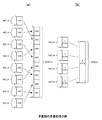
[S/P・スクランブル・8B/10B部の内部構成例]
図6は、S/P・スクランブル・8B/10B部12の構成を示すブロック図である。S/P・スクランブル・8B/10B部12は、各CH1〜CH8に一対一に対応した8個のブロック12−1〜12−8から成っている。
[S / P, scramble, 8B / 10B internal configuration example]
FIG. 6 is a block diagram showing the configuration of the S / P / scramble / 8B /
LinkAであるCH1,CH3,CH5,CH7用のブロック12−1,12−3,12−5,12−7は、ブロック12−1だけがブロック12−3,12−5,12−7と構成が相違する。一方、ブロック12−3,12−5,12−7は同一構成である(図ではブロック12−3について構成を記載し,12−5,12−7の構成の記載は省略している)。LinkBであるCH2,CH4,CH6,CH8用のブロック12−2,12−4,12−6,12−8は、全て同一構成である(図ではブロック12−2について構成を記載し,12−4,12−6,12−8の構成の記載は省略している)。また、各ブロックにおいて同一の処理を行う部分には同一符号を付している。 The blocks 12-1, 12-3, 12-5, and 12-7 for CH1, CH3, CH5, and CH7 that are LinkA are configured only by the block 12-1 as the blocks 12-3, 12-5, and 12-7. Is different. On the other hand, the blocks 12-3, 12-5, and 12-7 have the same configuration (in the figure, the configuration of the block 12-3 is described, and the description of the configuration of 12-5 and 12-7 is omitted). The blocks B-2, 12-4, 12-6, and 12-8 for CH2, CH4, CH6, and CH8, which are Link B, all have the same configuration (in the figure, the configuration is described for the block 12-2, and 12- 4, 12-6 and 12-8 are omitted.) In addition, the same reference numerals are given to portions that perform the same processing in each block.
最初に、LinkA用のブロック12−1,12−3,12−5,12−7について説明する。ブロック12−1,12−3,12−5,12−7では、入力したCH1,CH3,CH5,CH7のHD−SDI信号が、S/P(シリアル/パラレル)変換部21に送られる。S/P変換部21は、このHD−SDI信号をビットレート74.25Mbpsまたは74.25Mbps/1.001(以下単に74.25Mbpsと記載する)の20ビット幅のパラレル・デジタルデータにシリアル/パラレル変換する。そして、74.25MHzのクロックを抽出する。
First, the blocks 12-1, 12-3, 12-5, and 12-7 for Link A will be described. In blocks 12-1, 12-3, 12-5, and 12-7, the input HD-SDI signals of CH1, CH3, CH5, and CH7 are sent to an S / P (serial / parallel)
S/P変換部21によってシリアル/パラレル変換されたパラレル・デジタルデータは、TRS検出部22に送られる。S/P変換部21によって抽出された74.25MHzのクロックは、FIFOメモリ23に書込みクロックとして送られる。また、ブロック12−1内のS/P変換部21によって抽出された74.25MHzのクロックは、図2に示すPLL13にも送られる。
The parallel digital data subjected to serial / parallel conversion by the S /
TRS検出部22は、S/P変換部21から送られたパラレル・デジタルビデオ信号からタイミング基準信号SAV及びEAVを検出し、その検出結果に基づいてワード同期を確立する。
The
TRS検出部22の処理を経たパラレル・デジタルデータは、FIFOメモリ23に送られて、S/P変換部21からの74.25MHzのクロックによってFIFOメモリ23に書き込まれる。
The parallel digital data that has undergone the processing of the
図2のPLL13は、ブロック12−1内のS/P変換部21からの74.25MHzのクロックを1/2に分周した37.125MHzのクロックを、各ブロック12−1〜12−8内のFIFOメモリ23に読出しクロックとして送る。そして、各ブロック12−1〜12−8内のFIFOメモリ26及びブロック12−1内のFIFOメモリ27に書込みクロックとして送る。
The
またPLL13は、ブロック12−1内のS/P変換部21からの74.25MHzのクロックの周波数を9/8倍した83.5312MHzのクロックを、各ブロック12−1〜12−8内のFIFOメモリ26に読出しクロックとして送る。また、ブロック12−1内のFIFOメモリ27にも読出しクロックとして送る。そして、図2のFIFOメモリ16に書込みクロックとして送る。
In addition, the
またPLL13は、ブロック12−1内のS/P変換部21からの74.25MHzのクロックの周波数を9/4倍した167.0625MHzのクロックを、図2のFIFOメモリ16に読出しクロックとして送る。
Also, the
またPLL13は、ブロック12−1内のS/P変換部21からの74.25MHzのクロックの周波数を9倍した668.25MHzのクロックを、図2の多チャンネルデータ形成部17に読出しクロックとして送る。
The
図6に示すように、FIFOメモリ23からは、S/P変換部21からの74.25MHzのクロックによって書き込まれた20ビット幅のパラレル・デジタルデータが読出される。このとき、図2のPLL13からの37.125MHzのクロックにより、2サンプルを単位とした40ビット幅のパラレル・デジタルデータとして読み出されて、スクランブラ24に送られる。また、ブロック12−1では、FIFOメモリ23から読み出されたこの40ビット幅のパラレル・デジタルデータが、8B/10Bエンコーダ25にも送られる。
As shown in FIG. 6, from the
スクランブラ24は、自己同期型のスクランブラである。自己同期型スクランブル方式は、SMPTE292Mで採用されているスクランブル方式である。スクランブラ24は、送信側が、入力したシリアル信号を多項式とみなして9次の原始多項式
X9+X4+1
で順次割り算する。そして、割り算した結果である商を伝送することにより、統計的に伝送データのマーク率(1と0の割合)を平均1/2にする。このスクランブルは、原始多項式による信号の暗号化という意味も併せ持っている。この商をさらにX+1で割ることによって極性フリー(データとその反転データで同じ情報を持つこと)のデータにして送信する。受信側では、受信したシリアル信号にX+1を掛け、さらに上記原始多項式X9+X4+1を掛ける処理(デスクランブル)により、元のシリアル信号を再生する。
The
Divide sequentially with. Then, by transmitting the quotient obtained as a result of the division, the mark ratio (ratio of 1 and 0) of the transmission data is statistically halved. This scrambling also has the meaning of signal encryption using a primitive polynomial. The quotient is further divided by X + 1 to transmit the data as polarity-free (having the same information for the data and its inverted data). On the receiving side, the original serial signal is reproduced by a process (descrambling) of multiplying the received serial signal by X + 1 and further multiplying by the primitive polynomial X 9 + X 4 +1.
まず、スクランブラ24は、シリアル/パラレル変換部によってシリアル/パラレル変換されたLinkAの各水平ラインのデータのうち、000h,000h,000h,000hで規定されるタイミング基準信号SAVを所定の値に書き換える。本例では、000h,000h,000h,000hで規定されるタイミング基準信号SAVを、LinkAに含まれるタイミング基準信号EAVに続く、ライン番号LN0,LN0,LN1,LN1の順に書き換える。この処理については、図11を参照して後述する。
First, the
そして、スクランブラ24は、各水平ラインの全てのデータにスクランブルを掛けるのではなく、タイミング基準信号SAV,アクティブライン,タイミング基準信号EAV,ライン番号LN及び誤り検出符号CRCのデータのみにスクランブルを掛ける。一方、水平ブランキング期間のデータにはスクランブルを掛けない。そして、タイミング基準信号SAVの直前でスクランブラ内のレジスタの値を全て0にセットしてエンコードし、誤り検出符号CRCに続く10ビットまでのデータを出力する。
The
スクランブラ24でこうした処理を行うのは、次のような理由による。従来の自己同期型スクランブル方式では各水平ラインの全てのデータを途切れることなく送信するが、本発明では、自己同期型スクランブルを掛けた水平ブランキング期間のデータを送信しない。そのための方法としては、水平ブランキング期間も含めて各水平ラインの全てのデータにスクランブルを掛けるが水平ブランキング期間のデータだけは送信しない、という方法もある。しかし、その方法では、送信のスクランブラと受信のデスクランブラとでデータの連続性が保存されないので、受信側のデスクランブラでデータを再生する時にCRCの最後の数ビットで桁上がりの計算間違いを起こし、正確に誤り検出符号CRCが再生されない。また、データを送信しない水平ブランキング期間でスクランブラのクロックを止めることによって正確にCRCを再生できるようにするという方式もある。しかし、その方法を採用すると、CRCの計算時に次のタイミング基準信号SAVが必要となり、タイミング制御が困難になる等の問題が発生する。
The reason why such processing is performed by the
そこで、タイミング基準信号SAV,アクティブライン,タイミング基準信号EAV,ライン番号LN及び誤り検出符号CRCのデータのみにスクランブルを掛ける。また、タイミング基準信号SAVの直前でスクランブラ24内のレジスタの値を全て0にセットしてエンコードする。そして、誤り検出符号CRCに続く少なくとも数ビット(一例として10ビットとする)までのデータを出力するようにした。
Therefore, only the data of the timing reference signal SAV, the active line, the timing reference signal EAV, the line number LN, and the error detection code CRC is scrambled. Also, encoding is performed by setting all register values in the
こうすることにより、受信側の装置では、タイミング基準信号SAVの直前でデスクランブラ内のレジスタの値を全て0にセットしてデコードを開始できる。また、誤り検出符号CRCに続く少なくとも数ビットのデータにもデスクランブルを掛けることにより、掛け算回路であるデスクランブラの桁上がりを考慮した正確な計算を行って元のデータを再生できる。 In this way, the receiving apparatus can start decoding by setting all register values in the descrambler to 0 immediately before the timing reference signal SAV. Moreover, by multiplying at least several bits of data following the error detection code CRC by descrambling, the original data can be reproduced by performing an accurate calculation in consideration of the carry of the descrambler which is a multiplication circuit.
さらに、タイミング基準信号SAVの直前でスクランブラ内のレジスタの値を全て0にセットすると、スクランブルデータにパソロジカルパターンが発生しないことが計算によって判明した。パソロジカルパターンとは、自己同期型スクランブルを掛けた際に、シリアル伝送路上に、1水平ラインに亘り、所定のビット数で‘H’または‘L’が連続するパターン信号が発生するものである。例えば、図7(a)には、1ビットの‘H’に続いて19ビットの‘L’が続くパターン(あるいはその反転パターン)の信号が示される。また、図7(b)には、20ビットの‘H’が連続した後20ビットの‘L’が連続するパターン(あるいはその反転パターン)の信号が示される。 Further, it has been found by calculation that no pathological pattern is generated in the scrambled data when all the register values in the scrambler are set to 0 immediately before the timing reference signal SAV. A pathological pattern is a pattern signal in which 'H' or 'L' continues for a predetermined number of bits over one horizontal line on a serial transmission line when self-synchronizing scrambling is applied. . For example, FIG. 7A shows a signal of a pattern (or its inverted pattern) in which 19 bits of “L” follow 1 bit of “H”. FIG. 7B shows a signal of a pattern in which 20-bit ‘H’ continues and then 20-bit ‘L’ continues (or an inverted pattern thereof).
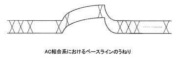
図7(a)のパターンやその反転パターンは、直流成分の多いパターンである。そして、10Gbpsというような高速な伝送レートを実現するためにはAC結合の伝送系を用いることが一般的である。しかし、AC結合の伝送系では、直流成分が多い場合に図8に示すようなベースラインのうねりを起こしてしまうので、受信側の装置で直流成分を再生することが必要になってしまう。 The pattern shown in FIG. 7A and its inverted pattern are patterns having a large direct current component. In order to realize a high transmission rate such as 10 Gbps, it is common to use an AC-coupled transmission system. However, in an AC-coupled transmission system, when there are many DC components, the baseline undulation as shown in FIG. 8 occurs, and it is necessary to regenerate the DC components by the receiving device.
図7(b)のパターンやその反転パターンは、0から1への遷移や1から0への遷移が少ないパターンなので、受信装置の側でシリアル信号からクロックを再生することが困難になってしまう。 Since the pattern in FIG. 7B and its inversion pattern have few transitions from 0 to 1 and transitions from 1 to 0, it is difficult for the receiver to reproduce the clock from the serial signal. .
これに対し、前述のように、タイミング基準信号SAVの直前でスクランブラ内のレジスタの値を全て0にセットすることにより、こうしたパソロジカルパターンが発生しないことが計算によって判明したので、伝送符号として良好な信号であるといえる。 On the other hand, as described above, it was found by calculation that such a pathological pattern does not occur by setting all the register values in the scrambler to 0 immediately before the timing reference signal SAV. It can be said that it is a good signal.
また、図9に示すように、タイミング基準信号SAV内の最後のワードであるXYZ(同一フレームの第1フィールド/第2フィールドを識別したり、SAVとEAVとを識別するためのワード)の下位2ビットは(0,0)になっている。しかし、例えば、ブロック12−1内のスクランブラ24ではこの下位2ビットを(0,0)にしたままスクランブルを掛ける。次に、ブロック12−3内のスクランブラ24ではこの下位2ビットを(0,1)に書き換えた後スクランブルを掛ける。次に、ブロック12−5内のスクランブラ24ではこの下位2ビットを(1,0)に書き換えた後スクランブルを掛ける。そして、ブロック12−7内のスクランブラ24ではこの下位2ビットを(1,1)に書き換えた後スクランブルを掛ける。このように、CH1,CH3,CH5,CH7のチャンネル毎にこの下位2ビットの値を変えてスクランブルを掛ける。
Further, as shown in FIG. 9, the lower word of XYZ (word for identifying the first field / second field of the same frame or the SAV and the EAV) is the last word in the timing reference signal SAV. The 2 bits are (0, 0). However, for example, the
このような処理を行うのは、次のような理由による。3840×2160/24P,25P,30P/4:4:4/12ビット信号がフラットな(画面全体でRGBの値がほぼ同じ)信号である場合を想定する。この場合、CH1,CH3,CH5,CH7とCH2,CH4,CH6,CH8とでデータ値が均一になると、EMI(電磁輻射)等が発生して好ましくない。これに対し、SAV内のXYZの下位2ビットの値をCH1,CH3,CH5,CH7のチャンネル毎に変えてスクランブルを掛ける場合を想定する。この場合、スクランブル後のデータは、XYZの下位2ビットを(0,0)にしたデータに加えて、(0,1),(1,0),(1,1)を生成多項式で割った結果を伝送することになる。このため、データの均一性を回避することが可能になる。 Such a process is performed for the following reason. Assume that the 3840 × 2160 / 24P, 25P, 30P / 4: 4: 4 / 12-bit signal is a flat signal (the RGB values are substantially the same throughout the screen). In this case, if the data values are uniform between CH1, CH3, CH5, CH7 and CH2, CH4, CH6, CH8, EMI (electromagnetic radiation) or the like is generated, which is not preferable. On the other hand, it is assumed that the lower two bits of XYZ in the SAV are changed for each channel of CH1, CH3, CH5, and CH7 and scrambled. In this case, the scrambled data is obtained by dividing (0, 1), (1, 0), (1, 1) by the generator polynomial in addition to the data in which the lower 2 bits of XYZ are set to (0, 0). The result will be transmitted. For this reason, it is possible to avoid data uniformity.
さらに、このようにXYZの下位2ビットの値をチャンネル毎に変えても、前述のようにタイミング基準信号SAVの直前でスクランブラ内のレジスタの値を全て0にセットすると、パソロジカルパターンが発生しないことが計算によって判明した。 Further, even if the lower 2 bits of XYZ are changed for each channel in this way, if all the register values in the scrambler are set to 0 immediately before the timing reference signal SAV as described above, a pathological pattern is generated. Not found by calculation.
このようにしてスクランブラ24でスクランブルを掛けられた40ビット幅のパラレル・デジタルデータは、図2のPLL13からの37.125MHzのクロックによってFIFOメモリ26に書き込まれる。その後、PLL13からの83.5312MHzのクロックによって40ビット幅のままFIFOメモリ26から読み出されて、図2に示す多重部14に送られる。
The 40-bit width parallel digital data scrambled by the
ブロック12−1内の8B/10Bエンコーダ25は、FIFOメモリ23から読み出された40ビット幅のパラレル・デジタルデータのうち、水平ブランキング期間のデータのみを8ビット/10ビットエンコーディングする。
The 8B /
8B/10Bエンコーダ25によって8ビット/10ビットエンコーディングされた50ビットのビット幅のパラレル・デジタルデータは、図2のPLL13からの37.125MHzのクロックによってFIFOメモリ27に書き込まれる。その後、PLL13からの83.5312MHzのクロックによって50ビット幅のままFIFOメモリ27から読み出されて、図2に示す多重部14に送られる。
The 50-bit width parallel digital data encoded by the 8B /
なお、ブロック12−1からのみ(すなわちCH1についてのみ)水平ブランキング期間のデータを多重部14に送る。ブロック12−3,12−5,12−7からは(CH3,CH5,CH7については)水平ブランキング期間のデータを多重部14に送らない。このようにするのは、データ量の制約上の理由からである。 Note that the data of the horizontal blanking period is sent to the multiplexing unit 14 only from the block 12-1 (that is, only for CH1). From the blocks 12-3, 12-5, and 12-7 (for CH3, CH5, and CH7), data in the horizontal blanking period is not sent to the multiplexing unit 14. This is done for the reason of restriction on the amount of data.
次に、LinkB用のブロック12−2,12−4,12−6,12−8について説明する。このブロックでは、入力したCH2,CH4,CH6,CH8のHD−SDI信号が、S/P変換部21及びTRS検出部22によってブロック12−1,12−3,12−5,12−7におけるのと同一の処理を施された後、抜き出し部28に送られる。
Next, the blocks 12-2, 12-4, 12-6, and 12-8 for LinkB will be described. In this block, the input HD-SDI signals of CH2, CH4, CH6, and CH8 are received in blocks 12-1, 12-3, 12-5, and 12-7 by the S /
抜き出し部28は、LinkBの各水平ラインのデータから、RGBのビット(図5に示したLinkBの1サンプルの20ビットのうちの、RGBの値を表している16ビット)を抜き出す回路である。このとき、抜き出し部28は、タイミング基準信号SAV,アクティブライン,タイミング基準信号EAV,ライン番号LN及び誤り検出符号CRCのデータのみからRGBのビットを抜き出す。
The
抜き出し部28によって抜き出された16ビット幅のパラレル・デジタルデータは、S/P変換部21からの74.25MHzのクロックによってFIFOメモリ23に書き込まれる。その後、図2のPLL13からの37.125MHzのクロックにより、2サンプルを単位とした32ビット幅のパラレル・デジタルデータとして読み出されて、K28.5挿入部29に送られる。
The 16-bit width parallel digital data extracted by the
K28.5挿入部29は、タイミング基準信号SAVまたはEAVの先頭部分に、2個の8ビットワードデータを挿入する。この8ビットワードデータは、8ビット/10ビットエンコーディングした際に、映像信号を表すワードデータとしては用いられない10ビットワードデータ(K28.5というコードネームで呼ばれるもの)に変換されるものである。
The K28.5
K28.5挿入部29の処理を経た32ビット幅のパラレル・デジタルデータは、8B/10Bエンコーダ30に送られる。8B/10Bエンコーダ30は、この32ビット幅のパラレル・デジタルデータを8ビット/10ビットエンコーディングして出力する。
The 32-bit width parallel digital data that has undergone the processing of the K28.5
2サンプルを単位とした32ビット幅のパラレル・デジタルデータを8B/10Bエンコーダ30で8ビット/10ビットエンコーディングさせるのは、次の理由による。つまり、10Gインタフェース規格であるSMPTE 435Mにおける50ビットのContent IDの上位の40ビットとの互換をとるためである。
The reason why the 8-bit / 10-bit encoding of the 32-bit-wide parallel digital data in units of 2 samples is performed by the 8B /
8B/10Bエンコーダ30によって8ビット/10ビットエンコーディングされた40ビット幅のパラレル・デジタルデータは、図2のPLL13からの37.125MHzのクロックによってFIFOメモリ26に書き込まれる。その後、PLL13からの83.5312MHzのクロックによって40ビット幅のままFIFOメモリ26から読み出されて、図2に示す多重部14に送られる。
The 40-bit width parallel digital data encoded by the 8B /
図2の多重部14は、S/P・スクランブル・8B/10B部12の各ブロック12−1〜12−8内のFIFOメモリ26から読み出されたCH1〜CH8の40ビット幅のパラレル・デジタルデータを、40ビット単位で、順に320ビット幅に多重する。この様子は図10(a)に示される。40ビット幅のパラレル・デジタルデータとは、タイミング基準信号SAV,アクティブライン,タイミング基準信号EAV,ライン番号LN及び誤り検出符号CRCのみのデータである。320ビット幅に多重する順は、CH2,CH1,CH4,CH3,CH6,CH5,CH8,CH7である。CH2,CH4,CH6,CH8は、8ビット/10ビットエンコーディングしたチャンネルである。CH1,CH3,CH5,CH7は、自己同期型スクランブルを掛けたチャンネルである。
2 is a 40-bit parallel digital signal of CH1 to CH8 read from the
このように、8ビット/10ビットエンコーディングしたデータを、自己同期型スクランブルを掛けたデータに40ビット毎にはさむことによって、パソロジカルパターンの発生を防止できる。このとき、スクランブル方式によるマーク率(0と1の割合)変動や、0−1、1−0の遷移の不安定さを解消できる。 In this way, the generation of a pathological pattern can be prevented by interposing the data encoded by 8 bits / 10 bits with the self-synchronized scrambled data every 40 bits. At this time, fluctuations in the mark ratio (ratio of 0 and 1) due to the scramble method and instability of transitions of 0-1 and 1-0 can be eliminated.
また、多重部14は、S/P・スクランブル・8B/10B部12のブロック12−1内のFIFOメモリ27から読み出されたCH1の水平ブランキング期間のみの50ビット幅のパラレル・デジタルデータを、4サンプル分多重して200ビット幅にする。この様子は、図10(b)に示す。
Further, the multiplexing unit 14 receives 50-bit parallel digital data of only the horizontal blanking period of CH1 read from the
多重部14によって多重されたこの320ビット幅のパラレル・デジタルデータと200ビット幅のパラレル・デジタルデータとは、データ長変換部15に送られる。データ長変換部15は、シフトレジスタを用いて構成されている。この320ビット幅のパラレル・デジタルデータを256ビット幅に変換したデータと、この200ビット幅のパラレル・デジタルデータを256ビット幅に変換したデータとを用いて、256ビット幅のパラレル・デジタルデータを形成する。そして、この256ビット幅のパラレル・デジタルデータをさらに128ビット幅に変換する。
The 320-bit width parallel digital data and the 200-bit width parallel digital data multiplexed by the multiplexing unit 14 are sent to the data
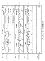
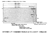
図11は、本実施の形態に係るベーシックストリームの伝送例を示す。
図11Aは、ベーシックストリームCH1,3,5,7を伝送する場合におけるデータ構造の例を示す。
フラットフィールドに対する安定性を向上させるために以下の処理を行う。すなわち、スクランブラ24は、スクランブルを掛ける前に、CH1,3,5,7のSAV(3FFh,3FFh,000h,000h,000h,000h,XYZh,XYZh)の(000h,000h,000h,000h)を、所定の値に書き換える。本例において、スクランブラ24は、フィールド51に含まれるライン番号(LN0,LN0,LN1,LN1)の内容を、フィールド52に含まれるSAV(000h,000h,000h,000h)の内容と書き換える処理を行う。つまり、CH1,3,5,7のSAVが多重してある同じラインのEAVに続く(LN0,LN0,LN1,LN1)に書き換えた後、スクランブルを掛ける。この処理によって、ベーシックストリームCH1,3,5,7は、それぞれSAVとアクティブビデオとEAVによって構成される映像信号に変換される。このとき、CXYZhの下位2ビットを、CH1,3,5,7でそれぞれ、(0,0),(0,1),(1,0),(1,1)に書き換える。
FIG. 11 shows an example of basic stream transmission according to the present embodiment.
FIG. 11A shows an example of a data structure when basic streams CH1, 3, 5, and 7 are transmitted.
The following processing is performed to improve stability against a flat field. That is, the
図11Bは、ベーシックストリームCH2,4,6,8を伝送する場合におけるデータ構造の例を示す。
ベーシックストリームCH2,4,6,8は、それぞれSAVとアクティブビデオとEAVによって構成されるHD−SDIフォーマット信号に変換される。ただし、このHD−SDIフォーマット信号は、8B/10B変換される。
FIG. 11B shows an example of a data structure when basic streams CH2, 4, 6, and 8 are transmitted.
The basic streams CH2, 4, 6, and 8 are converted into HD-SDI format signals each composed of SAV, active video, and EAV. However, this HD-SDI format signal is 8B / 10B converted.
図11Cは、10ビット8ワードのデータ構造の例を示す。
図11Aにおけるフィールド53と、図11Bにおけるフィールド54は、それぞれ、10ビット8ワードのデータに挿入される。
FIG. 11C shows an example of a data structure of 10 bits and 8 words.
The
このように、CH1,3,5,7はタイミング基準信号SAVとタイミング基準信号EAVとアクティブビデオのみスクランブルして多重される。このとき、SAVの直前でスクランブラのレジスタ値を全て0にセットしてエンコードし、タイミング基準信号EAV,ライン番号LN及び誤り検出符号CRCに続く10ビットまでのデータを送る。一方、受信側の後述するデスクランブラ41は、レジスタ値をSAVの直前で全て0にセットしてデコードを開始する。そして、10ビット余計に送られてきたデータにもデスクランブル処理する。これにより、掛け算回路であるデスクランブラの桁上がりを計算して元のデータを正確に再生できる。
Thus, CH1,3,5,7 is multiplexed with the scramble only timing reference signal SAV and timing reference signal EAV, active video. At this time, the register values of the scrambler are all set to 0 immediately before SAV for encoding, and data up to 10 bits following the timing reference signal EAV, line number LN, and error detection code CRC is sent. On the other hand, a
また、4k画面がフラットフィールドである場合、CH1,3,5,7とCH2,4,6,8のデータ値が同じになり、EMI等で好ましくない。このため、スクランブル時にSAV内の000h,000h,000h,000hを、入力HD−SDIの同一ライン内のEAVに続くCLN0,YLN0,CLN1,YLN1に書き換える。そして、XYZ下位2ビット(リザーブ0)をチャンネル毎に変えてスクランブルする。これによりデータの均一性を回避できる。XYZ下位2ビットは、受信側で元の00に戻すように処理すればよい。 When the 4k screen is a flat field, the data values of CH1, 3, 5, 7 and CH2, 4, 6, 8 are the same, which is not preferable for EMI or the like. Therefore, 000h, 000h, 000h, 000h in the SAV is rewritten to CLN0, YLN0, CLN1, YLN1 following the EAV in the same line of the input HD-SDI at the time of scrambling. Then, XYZ lower 2 bits (reserve 0) are changed for each channel and scrambled. This avoids data uniformity. The lower 2 bits of XYZ may be processed so as to return to the original 00 on the receiving side.
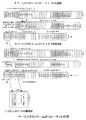
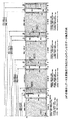
図12〜図14は、データ長変換部15によって形成される256ビット幅のパラレル・デジタルデータの構造を示す図である。
図12は30Pの場合の1ライン分のデータ構造を示す。
図13は25Pの場合の1ライン分のデータ構造を示す。
図14は24Pの場合の4ライン分のデータ構造を示す。
ただし、24Pの場合には、4ライン周期で最後のワードのビット数が128ビットになるので、4ライン分を描いている。
SMPTE435Mでは、フレームレート及びライン数が、CH1のHD−SDI信号と同じにされる。そして、S/P・スクランブル・8B/10B部12では、スクランブルと8B/10Bエンコーディングとを併用しているが、CH1にはスクランブル(SMPTE292Mで採用されているもの)を掛けている。したがって、図12〜図14に示したデータ構造は、基本的にはHD−SDI信号と同じになっている。
12 to 14 are diagrams showing the structure of 256-bit width parallel digital data formed by the data
FIG. 12 shows a data structure for one line in the case of 30P.
FIG. 13 shows a data structure for one line in the case of 25P.
FIG. 14 shows a data structure for four lines in the case of 24P.
However, in the case of 24P, since the number of bits of the last word is 128 bits in a 4-line cycle, 4 lines are drawn.
In SMPTE 435M, the frame rate and the number of lines are the same as those of the HD-SDI signal of CH1. In the S / P / scramble / 8B /
図12〜図14に示すように、1ライン分のデータは、次の3つの領域で構成されている。
・斜線を付した領域:CH2,CH1,CH4,CH3,CH6,CH5,CH8,CH7の順に40ビット単位で多重された各CH1〜CH8のタイミング基準信号SAV,アクティブライン,タイミング基準信号EAV,ライン番号LN及び誤り検出符号CRCのデータの領域
・ 白地の領域:8B/10BエンコーディングされたCH1の50ビットずつの水平ブランキング期間のデータの領域
・ ドット模様を付した領域:データ量調整のための付加データの領域
As shown in FIGS. 12 to 14, the data for one line is composed of the following three areas.
Areas with diagonal lines: timing reference signal SAV, active line, timing reference signal EAV, line of each of CH1 to CH8 multiplexed in units of 40 bits in the order of CH2, CH1, CH4, CH3, CH6, CH5, CH8, and CH7 Number LN and error detection code CRC data area White area: 8B / 10B encoded CH1 50-bit horizontal blanking period data area Dot pattern area: for data amount adjustment Additional data area
図2に示すように、データ長変換部15によって128ビット幅に変換されたパラレル・デジタルデータは、FIFOメモリ16に送られて、PLL13からの83.5312MHzのクロックによってFIFOメモリ16に書き込まれる。
As shown in FIG. 2, the parallel digital data converted into the 128-bit width by the data
FIFOメモリ16に書き込まれたこの128ビット幅のパラレル・デジタルデータは、図2のPLL13からの167.0625MHzのクロックにより、64ビット幅のパラレル・デジタルデータとしてFIFOメモリ16から読み出される。その後、多チャンネルデータ形成部17に送られる。
The 128-bit width parallel digital data written in the
多チャンネルデータ形成部17は、例えばXSBI(Ten gigabit Sixteen Bit Interface:10ギガビットイーサネット(登録商標)のシステムで使用される16ビットインタフェース)である。多チャンネルデータ形成部17は、FIFOメモリ16からの64ビット幅のパラレル・デジタルデータから、各々がビットレート668.25Mbpsを有する16チャンネル分のシリアル・デジタルデータを形成する。このとき、多チャンネルデータ形成部17は、PLL13からの668.25MHzのクロックを用いる。多チャンネルデータ形成部17によって形成された16チャンネルのシリアル・デジタルデータは、多重・P/S変換部18に送られる。
The multi-channel data forming unit 17 is, for example, XSBI (Tengigabit Sixteen Bit Interface: a 16-bit interface used in a 10 Gigabit Ethernet (registered trademark) system). The multi-channel data forming unit 17 forms 16-channel serial digital data each having a bit rate of 668.25 Mbps from the 64-bit parallel digital data from the
多重・P/S変換部18は、多チャンネルデータ形成部17からの16チャンネルのシリアル・デジタルデータを多重し、その多重したパラレル・デジタルデータをパラレル/シリアル変換する。これにより、668.25Mbps×16=10.692Gbpsのシリアル・デジタルデータを生成する。
The multiplexing / P /
図15は、この10.692Gbpsのシリアル・デジタルデータの1ライン分のデータ構造を示す図であり、図15(a)は24Pの場合の構造、図15(b)は25Pの場合の構造、図15(c)は30Pの場合の構造である。この図では、ライン番号LN及び誤り検出符号CRCを含めたものをSAV,アクティブライン及びEAVとして示すとともに、図12〜図14に示した付加データの領域を含めたものを水平ブランキング期間として示している。 FIG. 15 is a diagram showing a data structure for one line of the 10.692 Gbps serial digital data. FIG. 15A is a structure in the case of 24P, and FIG. 15B is a structure in the case of 25P. FIG. 15C shows a structure in the case of 30P. In this figure, the line number LN and the error detection code CRC are shown as SAV, active line and EAV, and the additional data area shown in FIGS. 12 to 14 is shown as a horizontal blanking period. ing.
24P,25P,30Pの場合の1ラインのビット数は、それぞれ下記式によって求められる。
10.692Gbps÷24フレーム/秒÷1125ライン/フレーム=396000ビット
10.692Gbps÷25フレーム/秒÷1125ライン/フレーム=380160ビット
10.692Gbps÷30フレーム/秒÷1125ライン/フレーム=316800ビット
The number of bits per line in the case of 24P, 25P, and 30P is obtained by the following formulas.
10.692 Gbps ÷ 24 frames / second ÷ 1125 lines / frame = 396000 bits 10.692 Gbps ÷ 25 frames / second ÷ 1125 lines / frame = 380 160 bits 10.692 Gbps ÷ 30 frames / second ÷ 1125 lines / frame = 316 800 bits
タイミング基準信号SAV,アクティブライン,タイミング基準信号EAV,ライン番号LN及び誤り検出符号CRCのビット数は、下記式によって求められる。
(1920T+12T)×36ビット×4ch×40/36=309120ビット
The number of bits of the timing reference signal SAV, the active line, the timing reference signal EAV, the line number LN, and the error detection code CRC is obtained by the following equation.
(1920T + 12T) × 36 bits × 4ch × 40/36 = 309120 bits
24P,25P,30Pの場合の水平ブランキング期間のビット数は、それぞれ下記式によって求められる。
(1)24Pの場合:396000ビット−309120ビット=86880ビット
(2750T−1920T−12T(SAV+EAV+LN+CRC))×20ビット×10/8=20450ビット
86880ビット>20450ビット
(2)25Pの場合:380160ビット−309120ビット=71040ビット
(2640T−1920T−12T(SAV+EAV+LN+CRC))×20ビット×10/8=17700ビット
71040ビット>17700ビット
(3)30Pの場合:316800ビット−309120ビット=7680ビット
(22T−1920T−12T(SAV+EAV+LN+CRC))×20ビット×10/8=6700ビット
7680ビット>6700ビット
The number of bits in the horizontal blanking period in the case of 24P, 25P, and 30P is obtained by the following equations, respectively.
(1) For 24P: 396000 bits-309120 bits = 86880 bits (2750T-1920T-12T (SAV + EAV + LN + CRC)) x 20 bits x 10/8 = 20450 bits 86880 bits> 20450 bits (2) For 25P: 380 160 bits- 309120 bits = 71040 bits (2640T-1920T-12T (SAV + EAV + LN + CRC)) × 20 bits × 10/8 = 17700 bits 71040 bits> 17700 bits (3) In the case of 30P: 316800 bits−309120 bits = 7680 bits (22T-1920T− 12T (SAV + EAV + LN + CRC)) × 20 bits × 10/8 = 6700 bits 7680 bits> 6700 bits
上記式に示したように、
24Pの場合、SMPTE435Mによる水平ブランキング期間のビット数である86880ビットの方が、20450ビットより大きい。
25Pの場合、SMPTE435Mによる水平ブランキング期間のビット数である71040ビットの方が、17700ビットより大きい。
30Pの場合、SMPTE435Mによる水平ブランキング期間のビット数である7680ビットの方が、6700ビットより大きい。
ここで、24Pの場合における20450ビットは、CH1の{水平ブランキング期間のデータ−(タイミング基準信号SAV,タイミング基準信号EAV,ライン番号LN及び誤り検出符号CRCのデータ)}のビット数である。以下、25Pの場合における17700ビット、30Pの場合における6700ビットも同様である。
このため、CH1の水平ブランキング期間のデータを多重することが可能である。
As shown in the above formula,
In the case of 24P, 86880 bits, which is the number of bits in the horizontal blanking period according to SMPTE 435M, is larger than 20450 bits.
In the case of 25P, 71040 bits, which is the number of bits in the horizontal blanking period according to SMPTE 435M, is larger than 17700 bits.
In the case of 30P, 7680 bits, which is the number of bits in the horizontal blanking period according to SMPTE 435M, is larger than 6700 bits.
Here, 20450 bits in the case of 24P is the number of bits of {data of horizontal blanking period- (data of timing reference signal SAV, timing reference signal EAV, line number LN and error detection code CRC)} of CH1. The same applies to 17700 bits in the case of 25P and 6700 bits in the case of 30P.
For this reason, it is possible to multiplex data in the horizontal blanking period of CH1.
図2に示すように、多重・P/S変換部18によって生成されたビットレート10.692Gbpsのシリアル・デジタルデータは、光電変換部19に送られる。そして、光電変換部19によって光信号に変換されたビットレート10.692Gbpsのシリアル・デジタルデータが、放送用カメラ1から図1の光ファイバーケーブル3経由でCCU2に伝送される。
As shown in FIG. 2, serial digital data having a bit rate of 10.692 Gbps generated by the multiplexing / P /
[CCUの内部構成例]
図16は、CCU2の回路構成のうち、本発明に関連する部分を示すブロック図である。CCU2には、図16に示すような回路が、各放送用カメラ1に一対一に対応して複数組設けられている。
[Example of internal configuration of CCU]
FIG. 16 is a block diagram showing a part related to the present invention in the circuit configuration of the
放送用カメラ1から光ファイバーケーブル3経由で伝送されたビットレート10.692Gbpsのシリアル・デジタルデータは、光電変換部31によって電気信号に変換された後、S/P変換・多チャンネルデータ形成部32に送られる。S/P変換・多チャンネルデータ形成部32は、例えば前述したXSBIである。
Serial digital data with a bit rate of 10.692 Gbps transmitted from the
S/P変換・多チャンネルデータ形成部32は、ビットレート10.692Gbpsのシリアル・デジタルデータをシリアル/パラレル変換する。そして、シリアル/パラレル変換したパラレル・デジタルデータから、各々がビットレート668.25Mbpsを有する16チャンネル分のシリアル・デジタルデータを形成する。そして、668.25MHzのクロックを抽出する。
The S / P conversion / multi-channel
S/P変換・多チャンネルデータ形成部32によって形成された16チャンネルのパラレル・デジタルデータは、多重部33に送られる。また、S/P変換・多チャンネルデータ形成部32によって抽出された668.25MHzのクロックは、PLL34に送られる。
The 16-channel parallel digital data formed by the S / P conversion / multi-channel
多重部33は、S/P変換・多チャンネルデータ形成部32からの16チャンネルのシリアル・デジタルデータを多重して、64ビット幅のパラレル・デジタルデータをFIFOメモリ35に送る。
The multiplexing
PLL34は、S/P変換・多チャンネルデータ形成部32からの668.25MHzのクロックを4分の1に分周した167.0625MHzのクロックをFIFOメモリ35に書込みクロックとして送る。
The
またPLL34は、S/P変換・多チャンネルデータ形成部32からの668.25MHzのクロックを8分の1に分周した83.5312MHzのクロックを、FIFOメモリ35に読出しクロックとして送る。そして、後述するデスクランブル・8B/10B・P/S部38内のFIFOメモリ44に書込みクロックとして送る。
Further, the
またPLL34は、S/P変換・多チャンネルデータ形成部32からの668.25MHzのクロックを18分の1に分周した37.125MHzのクロックを、デスクランブル・8B/10B・P/S部38内のFIFOメモリ44に読出しクロックとして送る。そして、デスクランブル・8B/10B・P/S部38内のFIFOメモリ45に書込みクロックとして送る。
Further, the
またPLL34は、S/P変換・多チャンネルデータ形成部32からの668.25MHzのクロックを9分の1に分周した74.25MHzのクロックを、デスクランブル・8B/10B・P/S部38内のFIFOメモリ45に読出しクロックとして送る。
In addition, the
FIFOメモリ35では、多重部33からの64ビット幅のパラレル・デジタルデータが、PLL34からの167.0625MHzのクロックによって書き込まれる。FIFOメモリ35に書き込まれたパラレル・デジタルデータは、PLL34からの83.5312MHzのクロックによって128ビット幅のパラレル・デジタルデータとして読み出されて、データ長変換部36に送られる。
In the
データ長変換部36は、シフトレジスタを用いて構成されており、この128ビット幅のパラレル・デジタルデータを、256ビット幅(図12〜図14に示した構造のデータ)に変換する。次に、タイミング基準信号SAVまたはEAVに挿入されているK28.5を検出することによって各ライン期間を判別する。次に、タイミング基準信号SAV,アクティブライン,タイミング基準信号EAV,ライン番号LN及び誤り検出符号CRCのデータを320ビット幅に変換する。そして、水平ブランキング期間のデータ(前述のように、8B/10BエンコーディングされたCH1の水平ブランキング期間のデータ)を200ビット幅に変換する。図12〜図14に示した付加データは破棄する。
The data
データ長変換部36によってデータ長を変換された320ビット幅のパラレル・デジタルデータと200ビット幅のパラレル・デジタルデータとは、分離部37に送られる。
The 320-bit width parallel digital data and the 200-bit width parallel digital data whose data length has been converted by the data
分離部37は、データ長変換部36からのこの320ビット幅のパラレル・デジタルデータを、放送用カメラ1内の多重部14(図2)によって多重される前の40ビットずつのCH1〜CH8のデータ(図10参照)に分離する。320ビット幅のパラレル・デジタルデータとは、タイミング基準信号SAV,アクティブライン,タイミング基準信号EAV,ライン番号LN及び誤り検出符号CRCのデータである。そして、各CH1〜CH8の40ビット幅のパラレル・デジタルデータを、デスクランブル・8B/10B・P/S部38に送る。
The
また分離部37は、データ長変換部36からのこの200ビット幅のパラレル・デジタルデータを、多重部14によって多重される前の50ビットずつのデータ(図10参照)に分離する。200ビット幅のパラレル・デジタルデータとは、8B/10BエンコーディングされたCH1の水平ブランキング期間のデータである。そして、この50ビット幅のパラレル・デジタルデータを、デスクランブル・8B/10B・P/S部38に送る。
The
[デスクランブル・8B/10B・P/S部の内部構成例]
図17は、デスクランブル・8B/10B・P/S部38の構成を示すブロック図である。デスクランブル・8B/10B・P/S部38は、各CH1〜CH8に一対一に対応した8個のブロック38−1〜38−8から成っている。
[Internal configuration example of descrambling /
FIG. 17 is a block diagram showing the configuration of the descrambling /
LinkAであるCH1,CH3,CH5,CH7用のブロック38−1,38−3,38−5,38−7は、ブロック38−1だけがブロック38−3,38−5,38−7と構成が相違する。そして、ブロック38−3,38−5,38−7は同一構成である。図17ではブロック38−3について構成を記載し,38−5,38−7の構成の記載は省略している。LinkBであるCH2,CH4,CH6,CH8用のブロック38−2,38−4,38−6,38−8は、全て同一構成である。図17ではブロック38−2について構成を記載し,38−4,38−6,38−8の構成の記載は省略している。また、各ブロックにおいて同一の処理を行う部分には同一符号を付している。 The blocks 38-1, 38-3, 38-5, and 38-7 for CH1, CH3, CH5, and CH7 that are Link A are configured only by the block 38-1 and the blocks 38-3, 38-5, and 38-7. Is different. The blocks 38-3, 38-5, and 38-7 have the same configuration. In FIG. 17, the configuration of the block 38-3 is described, and the configuration of the configurations 38-5 and 38-7 is omitted. The blocks B-2, 38-4, 38-6, and 38-8 for CH2, CH4, CH6, and CH8 that are Link B have the same configuration. In FIG. 17, the configuration of the block 38-2 is described, and the configuration of the configurations 38-4, 38-6, and 38-8 is omitted. In addition, the same reference numerals are given to portions that perform the same processing in each block.
最初に、LinkA用のブロック38−1,38−3,38−5,38−7について説明する。ブロック38−1,38−3,38−5,38−7では、入力したCH1,CH3,CH5,CH7の40ビット幅のパラレル・デジタルデータが、デスクランブラ41に送られる。40ビット幅のパラレル・デジタルデータとは、自己同期型スクランブルを掛けられたタイミング基準信号SAV,アクティブライン,タイミング基準信号EAV,ライン番号LN及び誤り検出符号CRCのデータである。
First, the blocks 38-1, 38-3, 38-5, and 38-7 for Link A will be described. In blocks 38-1, 38-3, 38-5, and 38-7, the input 40-bit parallel digital data of
デスクランブラ41は、自己同期型のデスクランブラである。デスクランブラ41は、送られたパラレル・デジタルデータにデスクランブルを掛けるが、タイミング基準信号SAVの直前でデスクランブラ41内のレジスタの値を全て0にセットしてデコードを開始する。そして、10ビット余計に送られてきたデータにもデスクランブル処理する。これにより、掛け算回路であるデスクランブラの桁上がりを計算して元のデータを正確に再生できる。また、誤り検出符号CRCに続く10ビットのデータにも自己同期型デスクランブルを掛ける。
The
これにより、自己同期型スクランブルを掛けた水平ブランキング期間のデータが送信されないにもかかわらず、掛け算回路であるデスクランブラ41の桁上がりを考慮した正確な計算を行って元のデータを再生できる。このことは、放送用カメラ1内のスクランブラ24(図6)の箇所でも説明している。
Thus, the original data can be reproduced by performing an accurate calculation considering the carry of the
またデスクランブラ41は、自己同期型スクランブルを掛けた後、CH1,CH3,CH5,CH7のチャンネル毎に値を変えてスクランブルを掛けられたビットの値を、元の値である(0,0)(図9参照)に変更する。このことは、タイミング基準信号SAV内のXYZの下位2ビットの値を元の値である(0,0)に変更する。この下位2ビットについては、上述したスクランブラ24の箇所で説明済みである。
ブロック38−1内のデスクランブラ41でデスクランブルを掛けられた40ビット幅のパラレル・デジタルデータは、セレクタ43に送られる。ブロック38−1では、入力した50ビット幅のパラレル・デジタルデータ(8B/10BエンコーディングされたCH1の水平ブランキング期間のデータ)が、8B/10Bデコーダ42に送られる。8B/10Bデコーダ42は、このパラレル・デジタルデータを8ビット/10ビットデコーディングする。8B/10Bデコーダ42によって8ビット/10ビットデコーディングされた40ビット幅のパラレル・デジタルデータが、セレクタ43に送られる。
The 40-bit width parallel digital data descrambled by the
セレクタ43は、デスクランブラ41からのパラレル・デジタルデータと8B/10Bデコーダ42からのパラレル・デジタルデータとを交互に選択する。これにより、各水平ラインの全てのデータを一本化した40ビット幅のパラレル・デジタルデータを形成して、この40ビット幅のパラレル・デジタルデータをFIFOメモリ44に送る。
The
他方、ブロック38−3,38−5,38−7では、50ビット幅のパラレル・デジタルデータは入力しないので8B/10Bデコーダ42及びセレクタ43は設けられていない。デスクランブラ41でデスクランブルを掛けられた40ビット幅のパラレル・デジタルデータは、そのままFIFOメモリ44に送られる。
On the other hand, the blocks 38-3, 38-5, and 38-7 are not provided with the 8B /
FIFOメモリ44に送られた40ビット幅のパラレル・デジタルデータは、PLL34(図16)からの83.5312MHzのクロックによってFIFOメモリ44に書き込まれる。その後、PLL34からの37.125MHzのクロックによって40ビット幅のままFIFOメモリ44から読み出されて、FIFOメモリ45に送られる。
The 40-bit width parallel digital data sent to the
FIFOメモリ45に送られた40ビット幅のパラレル・デジタルデータは、PLL34(図16)からの37.125MHzのクロックによってFIFOメモリ45に書き込まれる。その後、PLL34からの74.25MHzのクロックによって20ビット幅(図5に示したLinkAの1サンプル分ずつ)のパラレル・デジタルデータとしてFIFOメモリ45から読み出されて、P/S(パラレル/シリアル)変換部46に送られる。
The 40-bit width parallel digital data sent to the
P/S変換部46は、このパラレル・デジタルデータをビットレート1.485GbpsのHD−SDI信号にパラレル/シリアル変換して、HD−SDI信号を再生する。各ブロック38−1,38−3,38−5,38−7で再生されたCH1,CH3,CH5,CH7のHD−SDI信号は、図16の4k×2k再生部39に送られる。
P /
次に、LinkB用のブロック38−2,38−4,38−6,38−8について説明する。ブロック38−2,38−4,38−6,38−8では、入力したCH2,CH4,CH6,CH8の40ビット幅のパラレル・デジタルデータが、8B/10Bデコーダ47に送られる。40ビット幅のパラレル・デジタルデータとは、8B/10Bエンコーディングされたタイミング基準信号SAV,アクティブライン,タイミング基準信号EAV,ライン番号LN及び誤り検出符号CRCのデータである。
Next, the Block B blocks 38-2, 38-4, 38-6, and 38-8 will be described. In blocks 38-2, 38-4, 38-6, and 38-8, the input 40-bit parallel digital data of
8B/10Bデコーダ47は、このパラレル・デジタルデータを8ビット/10ビットデコーディングする。8B/10Bデコーダ47によって8ビット/10ビットデコーディングされた32ビット幅のパラレル・デジタルデータは、FIFOメモリ44に送られる。
The 8B /
FIFOメモリ44に送られた32ビット幅のパラレル・デジタルデータは、PLL34(図16)からの83.5312MHzのクロックによってFIFOメモリ44に書き込まれる。その後、PLL34からの37.125MHzのクロックによって32ビット幅のままFIFOメモリ44から読み出されて、FIFOメモリ45に送られる。
The 32-bit width parallel digital data sent to the
FIFOメモリ45に送られた32ビット幅のパラレル・デジタルデータは、PLL34(図16)からの37.125MHzのクロックによってFIFOメモリ45に書き込まれる。その後、PLL34からの74.25MHzのクロックによって16ビット幅(図5に示したLinkBの1サンプル分ずつのRGBのビット)のパラレル・デジタルデータとしてFIFOメモリ45から読み出されて、サンプルデータ形成部48に送られる。
The 32-bit width parallel digital data sent to the
サンプルデータ形成部48は、このLinkBのRGBのビットから、図5に示したR‘G’B‘n:0−1のビットナンバー0,1,8及び9の4ビットを付加したLinkBの20ビットずつの各サンプルのデータを形成する。このようにして形成された20ビット幅のパラレル・デジタルデータは、サンプルデータ形成部48からP/S変換部46に送られる。
The sample
P/S変換部46は、このパラレル・デジタルデータをビットレート1.485GbpsのHD−SDI信号にパラレル/シリアル変換して、HD−SDI信号を再生する。各ブロック38−2,38−4,38−6,38−8で再生されたCH2,CH4,CH6,CH8のHD−SDI信号は、図16の4k×2k再生部39に送られる。
P /
図16の4k×2k再生部39は、デスクランブル・8B/10B・P/S部38から送られたCH1〜CH8(LinkA及びLinkB)のHD−SDI信号に、所定の処理を施す回路である。この処理は、SMPTE 435Mに従って放送用カメラ1内のマッピング部11(図2)の処理(図4)と逆の処理を施すことにより、3840×2160/24P,25P,30P/4:4:4/12ビット信号を再生できる。
The 4k ×
4k×2k再生部39によって再生された3840×2160/24P,25P,30P/4:4:4/12ビット信号は、CCU2から出力されて、例えばVTR等(図示略)に送られる。
The 3840 × 2160 / 24P, 25P, 30P / 4: 4: 4 / 12-bit signal reproduced by the 4k ×
なお、このようにして各放送用カメラ1からCCU2に3840×2160/24P,25P,30P/4:4:4/12ビット信号に伝送されるだけでなく、CCU2からも前述のリターンビデオが光ファイバーケーブル3経由で各放送用カメラ1に伝送される。リターンビデオとは、他の放送用カメラ1で撮影中の映像を表示させるための映像信号である。リターンビデオは周知の技術を用いて生成されるので、そのための回路構成の説明は省略する。例えば、2チャンネル分のHD−SDI信号を、それぞれ8ビット/10ビットエンコーディングした後、多重してシリアル・デジタルデータに変換する処理によって、リターンビデオが生成される。
In this way, not only the
図18,図19は、以上に説明した3840×2160/24P,25P,30P/4:4:4/12ビット信号の伝送のための放送用カメラ1,CCU2の処理の概要をそれぞれ示す図である。
FIGS. 18 and 19 are diagrams respectively showing an outline of processing of the
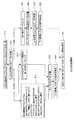
[放送用カメラの処理例]
図18に示すように、放送用カメラ1では、3840×2160/24P,25P,30P/4:4:4/12ビット信号が、CH1〜CH8のHD−SDI信号にマッピングされる(ステップS1)。CH1〜CH8は、LinkAであるCH1,CH3,CH5,CH7及びLinkBであるCH2,CH4,CH6,CH8である。放送用カメラ1のマッピングは、SMPTE 435MPart1の5.4 Octa Link 1.5 GbpsClassに従って行われる。このステップS1は、図2のマッピング部11の処理である。
[Broadcast camera processing example]
As shown in FIG. 18, in the
続いて、これらのHD−SDI信号をシリアル/パラレル変換する(ステップS2)。そして、LinkAについては、2サンプルを単位とした40ビット幅のデータにし(ステップS3)、その後自己同期型スクランブルを掛ける。このとき、タイミング基準信号SAV,アクティブライン,タイミング基準信号EAV,ライン番号LN及び誤り検出符号CRCのデータのみに自己同期型スクランブルを掛ける。そして、タイミング基準信号SAVの直前でスクランブラ内のレジスタの値を全て0にセットしてエンコードする。誤り検出符号CRCに続く10ビットまでのデータを出力する。また、タイミング基準信号SAV内のXYZの下位2ビットの値をチャンネル毎に変えて自己同期型スクランブルを掛ける。そして、各ラインの000h,000h,000h,000hで規定されるタイミング基準信号SAVを所定の値に書き換え、ライン毎に異なるデータを入れる。(ステップS4)。 Subsequently, these HD-SDI signals are serial / parallel converted (step S2). Then, LinkA is converted into 40-bit width data in units of 2 samples (step S3) and then subjected to self-synchronization scrambling. At this time, only the data of the timing reference signal SAV, the active line, the timing reference signal EAV, the line number LN, and the error detection code CRC are subjected to self-synchronization scrambling. Then, the register values in the scrambler are all set to 0 and encoded immediately before the timing reference signal SAV. Data up to 10 bits following the error detection code CRC is output. In addition, self-synchronous scrambling is performed by changing the lower two bits of XYZ in the timing reference signal SAV for each channel. Then, the timing reference signal SAV defined by 000h, 000h, 000h, 000h for each line is rewritten to a predetermined value, and different data is entered for each line. (Step S4).
また、CH1については、水平ブランキング期間のデータを8ビット/10ビットエンコーディングする(ステップS5)。 For CH1, the data in the horizontal blanking period is encoded by 8 bits / 10 bits (step S5).
他方、LinkBについては、各サンプルのデータからRGBのビットを抜き出す(ステップS6)。そして、このRGBのビットを、2サンプルを単位とした32ビット幅のデータにする(ステップS7)。そして、タイミング基準信号SAV,アクティブライン,タイミング基準信号EAV,ライン番号LN及び誤り検出符号CRCのデータのみを8B/10Bエンコーディングする(ステップS8)。このステップS2〜ステップS8は、図2及び図6のS/P・スクランブル・8B/10B部12の処理である。
On the other hand, for Link B, RGB bits are extracted from the data of each sample (step S6). The RGB bits are converted into 32-bit width data in units of 2 samples (step S7). Then, only the timing reference signal SAV, active line, timing reference signal EAV, line number LN, and error detection code CRC data are 8B / 10B encoded (step S8). Steps S2 to S8 are processes of the S / P / scramble / 8B /
このようにして自己同期型スクランブルを掛けたLinkAのデータと、このようにして8B/10BエンコーディングしたLinkBのデータとを多重する(ステップS9)。この多重したパラレル・デジタルデータから、ビットレート10.692Gbpsのシリアル・デジタルデータを生成する(ステップS10)。このステップS9は、図2の多重部14の処理であり、このステップS10は、図2のデータ長変換部15〜多重・P/S変換部18の処理である。
The LinkA data thus self-synchronized scrambled and the LinkB data thus 8B / 10B encoded are multiplexed (step S9). Serial digital data with a bit rate of 10.692 Gbps is generated from the multiplexed parallel digital data (step S10). This step S9 is a process of the multiplexing unit 14 in FIG. 2, and this step S10 is a process of the data
[CCUの処理例]
図19に示すように、CCU2では、ビットレート10.692Gbpsのシリアル・デジタルデータからパラレル・デジタルデータを生成する。(ステップS11)。そして、このパラレル・デジタルデータをLinkA,LinkBの各チャンネルのデータに分離する(ステップS12)。このステップS11は、図16のS/P変換・多チャンネルデータ形成部32〜データ長変換部36の処理であり、このステップS12は、図16の分離部37の処理である。
[CCU processing example]
As shown in FIG. 19, the
続いて、LinkAについては自己同期型デスクランブルを掛ける。ここでは、タイミング基準信号SAVの直前でデスクランブラ内のレジスタの値を全て0にセットしてデコードを開始するとともに、誤り検出符号CRCに続く10ビットのデータにも自己同期型デスクランブルを掛ける。また、自己同期型スクランブルを掛けた後、タイミング基準信号SAV内のXYZの下位2ビットの値を(0,0)に戻す。そして、異なるデータが入れられた各ラインのSAVのデータを元に戻す(ステップS13)。 Subsequently, self-synchronous descrambling is applied to LinkA. Here, all the register values in the descrambler are set to 0 immediately before the timing reference signal SAV to start decoding, and self-synchronous descrambling is also applied to 10-bit data following the error detection code CRC. Further, after the self-synchronization scrambling is applied, the value of the lower 2 bits of XYZ in the timing reference signal SAV is returned to (0, 0). Then, the SAV data of each line in which different data is entered is restored (step S13).
また、CH1については、水平ブランキング期間のデータを8B/10Bデコーディングする(ステップS14)。 For CH1, 8B / 10B decoding is performed on the data in the horizontal blanking period (step S14).
そして、1サンプル分ずつのデータを分離し(ステップS15)、分離したパラレル・デジタルデータをパラレル/シリアル変換して、LinkAのHD−SDI信号を再生する(ステップS16)。 Then, the data for each sample is separated (step S15), the parallel digital data thus separated is subjected to parallel / serial conversion, and the LinkA HD-SDI signal is reproduced (step S16).
他方、LinkBについては、8B/10Bデコーディングし(ステップS17)、1サンプル分ずつのRGBのビットを分離する(ステップS18)。続いて、このRGBのビットから、LinkBの各サンプルのデータを形成する(ステップS19)。そして、このようにして形成したパラレル・デジタルデータをパラレル/シリアル変換して、LinkBのHD−SDI信号を再生する(ステップS20)。このステップS13〜S20は、図16,18のデスクランブル・8B/10B・P/S部38の処理である。
On the other hand, 8B / 10B decoding is performed for LinkB (step S17), and RGB bits for one sample are separated (step S18). Subsequently, data of each sample of LinkB is formed from the RGB bits (step S19). The parallel digital data thus formed is converted from parallel to serial, and the LinkB HD-SDI signal is reproduced (step S20). Steps S13 to S20 are processes of the descrambling /
そして、再生したLinkA,LinkBのHD−SDI信号から、3840×2160/24P,25P,30P/4:4:4/12ビット信号を再生する(ステップS21)。このステップS21は、図16の4k×2k再生部39の処理である。
Then, 3840 × 2160 / 24P, 25P, 30P / 4: 4: 4 / 12-bit signals are reproduced from the reproduced Link A and Link B HD-SDI signals (step S21). This step S21 is a process of the 4k ×
以上に説明したように、このカメラ伝送システムでは、シリアル/パラレル変換されたLinkAの各水平ラインのデータのうち、000h,000h,000h,000hで規定されるタイミング基準信号SAVを所定の値に書き換える。このデータがスクランブルされた結果、フラットフィールドの映像信号であっても、タイミング基準信号SAVの値は異なる値となる。このため、あるデータがスクランブルされたことによってエラー信号を示すデータに変換されたとしても、このエラー信号を示すデータは連続しない。これにより、フラットフィールドの映像信号を好適に出力できるという効果がある。 As described above, in this camera transmission system, the timing reference signal SAV defined by 000h, 000h, 000h, 000h is rewritten to a predetermined value in the data of each horizontal line of Link A subjected to serial / parallel conversion. . As a result of this data being scrambled, the value of the timing reference signal SAV becomes a different value even for a flat field video signal. For this reason, even if certain data is scrambled and converted to data indicating an error signal, the data indicating the error signal is not continuous. Accordingly, there is an effect that a flat field video signal can be suitably output.
また、3840×2160/24P,25P,30P/4:4:4/12ビット信号を、所定の伝送規格に従って、CH1〜CH8(LinkA及びLinkB)のHD−SDI信号にマッピングする。本例における伝送規格は、SMPTE435M Part1の5.4 Octa Link 1.5 GbpsClassである。これにより、ビットレート10.692Gbpsのシリアル・デジタルデータに変換して伝送できる。このとき、3840×2160/24P,25P,30P/4:4:4/12bit信号がフラットなデータの場合に、第1,3,5,7chと第2,4,6,8chのデータ値が同じになり、EMI等好ましくない。このため、スクランブル時にSAV内の000h,000h,000h,000hを、入力HD−SDIの同一ライン内のEAVに続くCLN0,YLN0,CLN1,YLN1に書き換える。また、XYZ下位2ビット(リザーブ0)をチャンネル毎に変えてスクランブルする。これにより、Ch1,3,5,7毎だけではなく、フラットフィールドに対してもCh1,3,5,7のデータの均一性を回避できる。 Further, the 3840 × 2160 / 24P, 25P, 30P / 4: 4: 4 / 12-bit signal is mapped to the HD-SDI signals of CH1 to CH8 (Link A and Link B) according to a predetermined transmission standard. The transmission standard in this example is 5.4 Octa Link 1.5 Gbps Class of SMPTE 435M Part1. Thereby, it can be converted into serial digital data having a bit rate of 10.692 Gbps and transmitted. At this time, when the 3840 × 2160 / 24P, 25P, 30P / 4: 4: 4 / 12-bit signal is flat data, the data values of the first, third, fifth, seventh and second, fourth, fourth, sixth, and eighth channels are the same. It becomes the same, and EMI etc. are not preferable. Therefore, 000h, 000h, 000h, 000h in the SAV is rewritten to CLN0, YLN0, CLN1, YLN1 following the EAV in the same line of the input HD-SDI at the time of scrambling. Further, the lower 2 bits (reserve 0) of XYZ are changed for each channel and scrambled. Thereby, the uniformity of data of Ch1, 3, 5, and 7 can be avoided not only for every Ch1, 3, 5, and 7 but also for the flat field.
また、送信側である放送用カメラ1では、タイミング基準信号SAVの直前でスクランブラ24内のレジスタの値を全て0にセットしてエンコードし、誤り検出符号CRCに続く10ビットまでのデータを出力する。受信側であるCCU2では、タイミング基準信号SAVの直前でデスクランブラ41内のレジスタの値を全て0にセットしてデコードを開始するとともに、誤り検出符号CRCに続く10ビットのデータにもデスクランブルを掛ける。このため、自己同期型スクランブルを掛けた水平ブランキング期間のデータを送信しないにもかかわらず、受信側であるCCU2で正確に元のデータを再生できる。
Also, the
<2.変形例>
なお、以上の例ではカメラ伝送システムに本発明を適用しているが、本発明は、3840×2160/24P,25P,30P/4:4:4/12ビット信号を伝送するあらゆるシステムに適用してよい。
<2. Modification>
In the above example, the present invention is applied to a camera transmission system. However, the present invention is applied to any system that transmits 3840 × 2160 / 24P, 25P, 30P / 4: 4: 4/12 bit signals. It's okay.
また、SAV中の(000h,000h,000h,000h)の書き換える数値として、上述した実施の形態以外の数値を用いてもよい。例えば、000h,000h,000h,000hで規定されるタイミング基準信号SAVをランダムな数値に書き換えてもよい。また、000h,000h及びLinkAに含まれる前記タイミング基準信号EAVに続く、ライン番号LN0,LN1の順に書き換えてもよい。また、LinkAに含まれる前記タイミング基準信号EAVに続く、ライン番号LN0,LN1及び000h,000hの順に書き換えてもよい。 In addition, a numerical value other than the above-described embodiment may be used as a numerical value to be rewritten (000h, 000h, 000h, 000h) in SAV. For example, the timing reference signal SAV defined by 000h, 000h, 000h, 000h may be rewritten to a random numerical value. Further, the line numbers LN0 and LN1 may be rewritten in the order of the timing reference signal EAV included in 000h, 000h and LinkA. Further, the line numbers LN0, LN1 and 000h, 000h may be rewritten in the order following the timing reference signal EAV included in LinkA.
1…放送用カメラ、2…CCU、3…光ファイバーケーブル、11…マッピング部、12…S/P・スクランブル・8B/10B部、13…PLL、14…多重部、15…データ長変換部、16…FIFOメモリ、17…多チャンネルデータ形成部、18…多重・P/S変換部、19…光電変換部、21…S/P変換部、22…TRS検出部、23…FIFOメモリ、24…スクランブラ、25…8B/10Bエンコーダ、26…FIFOメモリ、27…FIFOメモリ、28…抜き出し部、30…8B/10Bエンコーダ、31…光電変換部、32…S/P変換・多チャンネルデータ形成部、33…多重部、34…PLL、35…FIFOメモリ、36…データ長変換部、37…分離部、38…デスクランブル・8B/10B・P/S部、39…2k再生部、41…デスクランブラ、42…8B/10Bデコーダ、43…セレクタ、44…FIFOメモリ、45…FIFOメモリ、46…P/S変換部、47…8B/10Bデコーダ、48…サンプルデータ形成部
DESCRIPTION OF
Claims (6)
前記シリアル/パラレル変換部によってシリアル/パラレル変換されたLinkAの各水平ラインのデータのうち、000h,000h,000h,000hで規定されるタイミング基準信号SAVを所定の値に書き換え、タイミング基準信号SAV内の最後のワードであるXYZの下位2ビットをチャンネル毎に変えて、タイミング基準信号SAV,アクティブライン,タイミング基準信号EAV,ライン番号LN及び誤り検出符号CRCのデータのみに自己同期型スクランブルを掛け、タイミング基準信号SAVの直前でスクランブラ内のレジスタの値を全て0にセットしてエンコードし、誤り検出符号CRCに続く少なくとも数ビットまでのデータを出力するスクランブラと、
前記シリアル/パラレル変換部によってシリアル/パラレル変換されたLinkBの各水平ラインのデータのうち、タイミング基準信号SAV,アクティブライン,タイミング基準信号EAV,ライン番号LN及び誤り検出符号CRCのデータのみからRGBのビットを抜き出す抜き出し部と、
前記抜き出し部によって抜き出されたLinkBのRGBのビットを8ビット/10ビットエンコーディングする8ビット/10ビットエンコーダと、
前記スクランブラによって自己同期型スクランブルを掛けられたLinkAのパラレル・デジタルデータと、前記8ビット/10ビットエンコーダによって8ビット/10ビットエンコーディングされたLinkBのパラレル・デジタルデータとを多重する多重部と、
前記多重部によって多重されたパラレル・デジタルデータから、所定のビットレートのシリアル・デジタルデータを生成するシリアル・デジタルデータ生成部と
を備える信号送信装置。 Serial / parallel conversion of serial digital video signals in HD-SDI format of CH1, CH3, CH5, and CH7 as links A and CH2, CH4, CH6, and CH8 as links B mapped according to a predetermined transmission standard. A parallel conversion unit;
Wherein among the data of the horizontal lines of LinkA that is serial / parallel conversion by the serial / parallel converter, 000h, 000h, 000h, rewrites the timing reference signal SAV specified as 000h to a predetermined value, the timing reference signal By changing the lower 2 bits of XYZ, which is the last word in SAV, for each channel , self-synchronization scrambling is performed only on data of timing reference signal SAV, active line, timing reference signal EAV, line number LN and error detection code CRC. A scrambler that encodes by setting all the register values in the scrambler to 0 immediately before the timing reference signal SAV and outputs data of at least several bits following the error detection code CRC;
Of the data of each horizontal line of LinkB serial / parallel converted by the serial / parallel converter, only the data of RGB from only the data of the timing reference signal SAV, active line, timing reference signal EAV, line number LN and error detection code CRC is obtained. An extraction part for extracting the bit;
An 8-bit / 10-bit encoder that performs 8-bit / 10-bit encoding of LinkB RGB bits extracted by the extraction unit;
A multiplexing unit that multiplexes Link A parallel digital data self-synchronized by the scrambler, and Link B parallel digital data encoded by the 8-bit / 10-bit encoder by the 8-bit / 10-bit encoder;
A signal transmission apparatus comprising: a serial digital data generation unit that generates serial digital data of a predetermined bit rate from parallel digital data multiplexed by the multiplexing unit.
前記000h,000h,000h,000hで規定されるタイミング基準信号SAVを、LinkAに含まれるタイミング基準信号EAVに続く、ライン番号LN0,LN0,LN1,LN1の順に書き換える
信号送信装置。 The signal transmission device according to claim 1,
A signal transmission device that rewrites the timing reference signal SAV defined by 000h, 000h, 000h, 000h in the order of line numbers LN0, LN0, LN1, and LN1 following the timing reference signal EAV included in LinkA.
前記000h,000h,000h,000hで規定されるタイミング基準信号SAVをランダムな数値に書き換える
信号送信装置。 The signal transmission device according to claim 1,
A signal transmission device that rewrites the timing reference signal SAV defined by 000h, 000h, 000h, 000h to a random numerical value.
前記000h,000h,000h,000hで規定されるタイミング基準信号SAVを、000h,000h及びLinkAに含まれるタイミング基準信号EAVに続く、ライン番号LN0,LN1の順に書き換える
信号送信装置。 The signal transmission device according to claim 1,
A signal transmission device that rewrites the timing reference signal SAV defined by the 000h, 000h, 000h, and 000h in the order of line numbers LN0 and LN1 following the timing reference signal EAV included in 000h, 000h and LinkA.
前記000h,000h,000h,000hで規定されるタイミング基準信号SAVを、LinkAに含まれるタイミング基準信号EAVに続く、ライン番号LN0,LN1及び000h,000hの順に書き換える
信号送信装置。 The signal transmission device according to claim 1,
A signal transmission device that rewrites the timing reference signal SAV defined by 000h, 000h, 000h, 000h in the order of line numbers LN0, LN1, and 000h, 000h following the timing reference signal EAV included in LinkA.
前記第1のステップでシリアル/パラレル変換したLinkAの各水平ラインのデータのうち、000h,000h,000h,000hで規定されるタイミング基準信号SAVを所定の値に書き換え、タイミング基準信号SAV内の最後のワードであるXYZの下位2ビットをチャンネル毎に変えて、タイミング基準信号SAV,アクティブライン,タイミング基準信号EAV,ライン番号LN及び誤り検出符号CRCのデータのみに自己同期型スクランブルを掛けるステップであって、タイミング基準信号SAVの直前でスクランブラ内のレジスタの値を全て0にセットしてエンコードし、誤り検出符号CRCに続く少なくとも数ビットまでのデータを出力する第2のステップと、
前記第1のステップでシリアル/パラレル変換したLinkBの各水平ラインのデータのうち、タイミング基準信号SAV,アクティブライン,タイミング基準信号EAV,ライン番号LN及び誤り検出符号CRCのデータのみからRGBのビットを抜き出す第3のステップと、
前記第3のステップで抜き出したLinkBのRGBのビットを8ビット/10ビットエンコーディングする第4のステップと、
前記第2のステップで自己同期型スクランブルを掛けたLinkAのパラレル・デジタルデータと、前記第4のステップで8ビット/10ビットエンコーディングしたLinkBのパラレル・デジタルデータとを多重する第5のステップと、
前記第5のステップで多重したパラレル・デジタルデータから、所定のビットレートのシリアル・デジタルデータを生成する第6のステップと、を有する
信号送信方法。 A first serial / parallel conversion is performed on serial digital video signals in the HD-SDI format of CH1, CH3, CH5, and CH7 that are LinkA mapped according to a predetermined transmission standard and CH2, CH4, CH6, and CH8 that are LinkB. And the steps
Wherein among the data of the horizontal lines of LinkA that serial / parallel conversion in the first step, 000h, 000h, 000h, conversion example write timing reference signal SAV to a predetermined value defined by 000h, the timing reference signal SAV Step of changing self-synchronous scramble only to timing reference signal SAV, active line, timing reference signal EAV, line number LN and error detection code CRC data by changing lower 2 bits of XYZ which is the last word of each channel for each channel A second step of encoding by setting all register values in the scrambler to 0 immediately before the timing reference signal SAV, and outputting data of at least several bits following the error detection code CRC;
Of the link B horizontal line data serial / parallel converted in the first step, RGB bits are obtained only from the data of the timing reference signal SAV, active line, timing reference signal EAV, line number LN and error detection code CRC. A third step to extract,
A fourth step of encoding 8 bits / 10 bits of RGB bits of LinkB extracted in the third step;
A fifth step of multiplexing the LinkA parallel digital data subjected to self-synchronization scrambling in the second step and the LinkB parallel digital data encoded in 8 bits / 10 bits in the fourth step;
And a sixth step of generating serial digital data of a predetermined bit rate from the parallel digital data multiplexed in the fifth step.
Priority Applications (7)
| Application Number | Priority Date | Filing Date | Title |
|---|---|---|---|
| JP2008263243A JP4702425B2 (en) | 2008-10-09 | 2008-10-09 | Signal transmitting apparatus and signal transmitting method |
| AT09252322T ATE493843T1 (en) | 2008-10-09 | 2009-09-30 | SIGNAL TRANSMISSION DEVICE AND SIGNAL TRANSMISSION METHOD |
| BRPI0903985-6A BRPI0903985A2 (en) | 2008-10-09 | 2009-09-30 | Signal transmission apparatus and method |
| DE200960000497 DE602009000497D1 (en) | 2008-10-09 | 2009-09-30 | Signal transmission device and signal transmission method |
| EP20090252322 EP2175637B1 (en) | 2008-10-09 | 2009-09-30 | Signal transmission apparatus and signal transmission method |
| US12/574,743 US8396215B2 (en) | 2008-10-09 | 2009-10-07 | Signal transmission apparatus and signal transmission method |
| CN200910179402A CN101719807A (en) | 2008-10-09 | 2009-10-09 | Signal transmission apparatus and signal transmission method |
Applications Claiming Priority (1)
| Application Number | Priority Date | Filing Date | Title |
|---|---|---|---|
| JP2008263243A JP4702425B2 (en) | 2008-10-09 | 2008-10-09 | Signal transmitting apparatus and signal transmitting method |
Publications (2)
| Publication Number | Publication Date |
|---|---|
| JP2010093658A JP2010093658A (en) | 2010-04-22 |
| JP4702425B2 true JP4702425B2 (en) | 2011-06-15 |
Family
ID=41441502
Family Applications (1)
| Application Number | Title | Priority Date | Filing Date |
|---|---|---|---|
| JP2008263243A Active JP4702425B2 (en) | 2008-10-09 | 2008-10-09 | Signal transmitting apparatus and signal transmitting method |
Country Status (7)
| Country | Link |
|---|---|
| US (1) | US8396215B2 (en) |
| EP (1) | EP2175637B1 (en) |
| JP (1) | JP4702425B2 (en) |
| CN (1) | CN101719807A (en) |
| AT (1) | ATE493843T1 (en) |
| BR (1) | BRPI0903985A2 (en) |
| DE (1) | DE602009000497D1 (en) |
Cited By (1)
| Publication number | Priority date | Publication date | Assignee | Title |
|---|---|---|---|---|
| JP2015119348A (en) * | 2013-12-18 | 2015-06-25 | 日本放送協会 | Video data transmission device and transmission method |
Families Citing this family (10)
| Publication number | Priority date | Publication date | Assignee | Title |
|---|---|---|---|---|
| JP5879545B2 (en) | 2010-10-12 | 2016-03-08 | パナソニックIpマネジメント株式会社 | Transmission circuit, reception circuit, transmission method, reception method, communication system and communication method thereof |
| CN102065208B (en) * | 2010-12-08 | 2013-03-13 | 南开大学 | Realization method of digital audio and video signal SerDes |
| JP5870508B2 (en) * | 2011-05-19 | 2016-03-01 | ソニー株式会社 | Signal transmission device, signal transmission method, signal reception device, signal reception method, and signal transmission system |
| JP2012253689A (en) * | 2011-06-06 | 2012-12-20 | Sony Corp | Signal transmitter, signal transmission method, signal receiver, signal reception method and signal transmission system |
| WO2013042264A1 (en) | 2011-09-22 | 2013-03-28 | Necディスプレイソリューションズ株式会社 | Video processing device and video processing method |
| CN103402068B (en) * | 2013-08-09 | 2016-08-17 | 西安电子科技大学 | Uncompressed formula audio/video player system and player method |
| CN104699219B (en) * | 2013-12-10 | 2020-06-23 | 联想(北京)有限公司 | Electronic equipment and information processing method |
| US20160112723A1 (en) * | 2014-10-17 | 2016-04-21 | Ross Video Limited | Transfer of video and related data over serial data interface (sdi) links |
| US9967476B2 (en) | 2014-10-17 | 2018-05-08 | Ross Video Limited | Parallel video effects, mix trees, and related methods |
| CN105680871B (en) * | 2016-04-07 | 2018-09-28 | 武汉芯泰科技有限公司 | For data serial transmission and go here and there, serioparallel exchange device |
Citations (3)
| Publication number | Priority date | Publication date | Assignee | Title |
|---|---|---|---|---|
| JP2008028651A (en) * | 2006-07-20 | 2008-02-07 | Sony Corp | Signal processor and signal processing method |
| JP2008042408A (en) * | 2006-08-03 | 2008-02-21 | Sony Corp | Signal processor and signal processing method |
| JP2008099189A (en) * | 2006-10-16 | 2008-04-24 | Sony Corp | Signal processor and signal processing method |
Family Cites Families (1)
| Publication number | Priority date | Publication date | Assignee | Title |
|---|---|---|---|---|
| JP4645638B2 (en) * | 2007-11-22 | 2011-03-09 | ソニー株式会社 | Signal transmitting apparatus, signal transmitting method, signal receiving apparatus, and signal receiving method |
-
2008
- 2008-10-09 JP JP2008263243A patent/JP4702425B2/en active Active
-
2009
- 2009-09-30 EP EP20090252322 patent/EP2175637B1/en active Active
- 2009-09-30 AT AT09252322T patent/ATE493843T1/en not_active IP Right Cessation
- 2009-09-30 DE DE200960000497 patent/DE602009000497D1/en active Active
- 2009-09-30 BR BRPI0903985-6A patent/BRPI0903985A2/en not_active IP Right Cessation
- 2009-10-07 US US12/574,743 patent/US8396215B2/en active Active
- 2009-10-09 CN CN200910179402A patent/CN101719807A/en active Pending
Patent Citations (3)
| Publication number | Priority date | Publication date | Assignee | Title |
|---|---|---|---|---|
| JP2008028651A (en) * | 2006-07-20 | 2008-02-07 | Sony Corp | Signal processor and signal processing method |
| JP2008042408A (en) * | 2006-08-03 | 2008-02-21 | Sony Corp | Signal processor and signal processing method |
| JP2008099189A (en) * | 2006-10-16 | 2008-04-24 | Sony Corp | Signal processor and signal processing method |
Cited By (1)
| Publication number | Priority date | Publication date | Assignee | Title |
|---|---|---|---|---|
| JP2015119348A (en) * | 2013-12-18 | 2015-06-25 | 日本放送協会 | Video data transmission device and transmission method |
Also Published As
| Publication number | Publication date |
|---|---|
| EP2175637B1 (en) | 2010-12-29 |
| ATE493843T1 (en) | 2011-01-15 |
| CN101719807A (en) | 2010-06-02 |
| EP2175637A1 (en) | 2010-04-14 |
| US8396215B2 (en) | 2013-03-12 |
| DE602009000497D1 (en) | 2011-02-10 |
| US20100091989A1 (en) | 2010-04-15 |
| BRPI0903985A2 (en) | 2011-02-01 |
| JP2010093658A (en) | 2010-04-22 |
Similar Documents
| Publication | Publication Date | Title |
|---|---|---|
| JP4702425B2 (en) | Signal transmitting apparatus and signal transmitting method | |
| JP4645638B2 (en) | Signal transmitting apparatus, signal transmitting method, signal receiving apparatus, and signal receiving method | |
| JP4557016B2 (en) | Signal transmitter | |
| JP4506852B2 (en) | Signal input device and signal input method | |
| JP4692576B2 (en) | Signal transmitting apparatus and signal transmitting method | |
| JP4165587B2 (en) | Signal processing apparatus and signal processing method | |
| US8854540B2 (en) | Signal transmission apparatus, signal transmission method, signal reception apparatus, signal reception method, and signal transmission system | |
| JP6221606B2 (en) | Signal processing apparatus, signal processing method, program, and signal transmission system | |
| US8982959B2 (en) | Signal transmission apparatus, signal transmission method, signal reception apparatus, signal reception method, and signal transmission system | |
| US9071375B2 (en) | Signal transmitting apparatus, signal transmitting method, signal receiving apparatus, signal receiving method, and signal transmission system | |
| US11044439B2 (en) | Signal processing apparatus, signal processing method, program, and signal transmission system | |
| US20110273623A1 (en) | Signal transmission apparatus and signal transmission method | |
| JP4910621B2 (en) | Signal processing apparatus and signal processing method | |
| US7477168B2 (en) | Apparatus for and method of processing data | |
| JP2007274533A (en) | Transmission apparatus for serial transmission, scramble processing method, and reception apparatus and system | |
| JP2014168152A (en) | Signal transmitter, signal receiver, and signal transmission system |
Legal Events
| Date | Code | Title | Description |
|---|---|---|---|
| A131 | Notification of reasons for refusal |
Free format text: JAPANESE INTERMEDIATE CODE: A131 Effective date: 20100629 |
|
| A521 | Request for written amendment filed |
Free format text: JAPANESE INTERMEDIATE CODE: A523 Effective date: 20100820 |
|
| TRDD | Decision of grant or rejection written | ||
| A01 | Written decision to grant a patent or to grant a registration (utility model) |
Free format text: JAPANESE INTERMEDIATE CODE: A01 Effective date: 20110208 |
|
| A61 | First payment of annual fees (during grant procedure) |
Free format text: JAPANESE INTERMEDIATE CODE: A61 Effective date: 20110221 |
|
| R151 | Written notification of patent or utility model registration |
Ref document number: 4702425 Country of ref document: JP Free format text: JAPANESE INTERMEDIATE CODE: R151 |
|
| R250 | Receipt of annual fees |
Free format text: JAPANESE INTERMEDIATE CODE: R250 |
|
| R250 | Receipt of annual fees |
Free format text: JAPANESE INTERMEDIATE CODE: R250 |
|
| R250 | Receipt of annual fees |
Free format text: JAPANESE INTERMEDIATE CODE: R250 |
|
| R250 | Receipt of annual fees |
Free format text: JAPANESE INTERMEDIATE CODE: R250 |
|
| R250 | Receipt of annual fees |
Free format text: JAPANESE INTERMEDIATE CODE: R250 |
|
| R250 | Receipt of annual fees |
Free format text: JAPANESE INTERMEDIATE CODE: R250 |
|
| R250 | Receipt of annual fees |
Free format text: JAPANESE INTERMEDIATE CODE: R250 |