JP4688984B2 - Silicon wafer and crystal growth method - Google Patents
Silicon wafer and crystal growth method Download PDFInfo
- Publication number
- JP4688984B2 JP4688984B2 JP36770297A JP36770297A JP4688984B2 JP 4688984 B2 JP4688984 B2 JP 4688984B2 JP 36770297 A JP36770297 A JP 36770297A JP 36770297 A JP36770297 A JP 36770297A JP 4688984 B2 JP4688984 B2 JP 4688984B2
- Authority
- JP
- Japan
- Prior art keywords
- crystal
- carbon
- pulling
- atoms
- wafer
- Prior art date
- Legal status (The legal status is an assumption and is not a legal conclusion. Google has not performed a legal analysis and makes no representation as to the accuracy of the status listed.)
- Expired - Fee Related
Links
Images
Landscapes
- Crystals, And After-Treatments Of Crystals (AREA)
Description
【0001】
【発明の属する技術分野】
本発明は、半導体デバイスの素材として使用されるシリコンウエーハ、及びそのウエーハを製造するための結晶育成方法に関する。
【0002】
【従来の技術】
半導体デバイスの素材として使用されるシリコンウエーハは、主にCZ法により育成されたシリコン単結晶から採取される。CZ法とは、周知の如く、石英坩堝内に生成されたシリコンの原料融液に種結晶を漬け、種結晶及び石英坩堝を逆方向に回転させながら種結晶を引き上げることにより、その下にシリコンの単結晶を育成する方法である。
【0003】
このようなCZ法による育成プロセスを経て製造されたシリコンウエーハは、熱酸化処理を受けたときに、OSFリングと呼ばれるリング状の酸化誘起積層欠陥を生じることが知られている。OSFリングはそれ自体が半導体素子の特性を劣化させる原因になるだけでなく、リングの外側と内側では物性が異なり、OSFリングの外側には格子間原子の凝集が原因とされる転位クラスタが発生するが、OSFリングの内側は比較的健全とされている。一方、このOSFリングについては、引き上げ速度が速くなるに連れて単結晶の外周側へ移動することが知られている。
【0004】
このような事情から、これまでは、OSFリングが、デバイス形成の際の有効部から除外される結晶最外周部に分布するような高速引き上げ条件で単結晶の育成を行っており、生産性の点からもこの高速引き上げは好ましいものである。
【0005】
しかし、OSFリングの内側にも問題がないわけではない。この部分には空孔の凝集が原因とされる空孔クラスタが発生している。この欠陥は、ウエーハの表面をエッチングすると小さなピットとなって現れるが、非常に小さなため、これまでは特に問題視されることはなかった。しかし、近年の著しい集積度の増大に伴ってパターン幅が非常に微細化したため、高グレードのウエーハではこの空孔クラスタさえも問題になり始めた。
【0006】
この空孔クラスタは、ウエーハ上にシリコン単結晶の薄膜を成長させた所謂エピタキシャルウエーハには殆ど発生しないが、このウエーハは非常に高価であるため、CZ法による単結晶の引き上げで空孔クラスタの少ない結晶を育成することが要求されるようになり、この観点から、高グレードの結晶育成では、これまでとは逆に引き上げ速度を遅くし、OSFリングを引き上げ結晶の最外周部より内側に発生させて欠陥部分を中心部に集中させるか、若しくは中心部で消滅させて空孔クラスタ個数の低減を図る低速引き上げ法が考えられている。
【0007】
【発明が解決しようとする課題】
しかしながら、この低速引き上げでは、高速引き上げに比べて生産性が著しく低下するという問題がある。また、引き上げ速度を遅くすることにより、引き上げ時間が長くなるため、有転位化を生じる危険性が大きくなり、この有転位化による歩留りの低下も問題になる。
【0008】
従って、この低速引き上げによる育成工程を経て製造されるシリコンウエーハは、高速引き上げによるものに比べて高価となる。
【0009】
ちなみに、OSFリングを結晶半径方向の1/2位置に発生させる場合は、最大引き上げ速度の0.7倍程度の低速で引き上げを行うことが必要とされており、OSFリングを結晶中心部で消滅させる場合は、最大引き上げ速度の0.6倍程度の低速引き上げが必要とされている。
【0010】
本発明の目的は空孔クラスタが少なく、しかも製造コストが安いシリコンウエーハを提供することにある。
【0011】
本発明の他の目的は、引き上げ速度を低下させずとも、空孔クラスタの発生を抑制することができる結晶育成方法を提供することにある。
【0012】
【課題を解決するための手段】
ところで、半導体デバイス材料として使用される一般のシリコン単結晶では、炭素は不純物として扱われており、不可避的に混入する分を除き、この炭素は含まれていないのが通例である。不可避的に混入する炭素としては、大きく別けてシリコンの多結晶原料に不純物として含まれるものと、単結晶の育成過程で周囲のグラファイト製ヒータから混入するものの2つがあるが、その濃度は一般のウエーハで0.5×10¹⁶atoms/cm3 以下である。また、一部ではウエーハを強化するために炭素を積極的に添加することも行われているが、そのような炭素強化型ウエーハでも、炭素濃度は1×10¹⁶atoms/cm3 未満である。
【0013】
ところが、この炭素は意図的に多量添加された場合に、空孔クラスタの発生を抑制する因子になり得ることが本発明者らによる種々の実験調査から明らかとなった。これを踏まえて、本発明者らは空孔クラスタに及ぼす炭素濃度の影響を子細に調査した結果、炭素濃度が1×10¹⁶atoms/cm3 以上の場合に、OSFリング内側での空孔クラスタの発生が顕著に抑制され、低速引き上げが必要とされなくなることを知見した。
【0014】
炭素によって空孔クラスタの発生が抑制される理由は現時点では定かではないが、一応次のように考えられる。炭素起因の析出物により、その周辺のSi格子が圧縮して歪み、この歪みを緩和させるのに空孔が消費されるためと考えられる。
【0015】
炭素が積極添加されたウエーハを簡易に製造するためには、炭素がドープされた原料融液から単結晶を引き上げる必要がある。本発明者らは、坩堝内の原料融液に炭素をドープする方法についても調査検討した。その結果、以下の知見を得ることができた。
【0016】
炭素はシリコンより融点が高いために、原料融液に炭素粉末を添加する方法では、溶け残りや飛散が生じ、原料融液の炭素濃度が正確に管理されないだけでなく、溶け残った粉末や飛散した粉末が単結晶に取り込まれて有転位化を生じるという問題がある。
【0017】
本発明者らはこの問題を解決するために炭素粉末の添加方法について検討した結果、坩堝内で多結晶原料を溶解して原料融液を生成する際に、多結晶原料の装填に先立って坩堝の内底面上に炭素粉末を敷いておくと、その粉末の飛散が防止されるだけでなく、高温の坩堝底部によって炭素粉末が効率的に加熱され、その粉末の溶け残りが生じなくなることを知見した。
【0018】
本発明のシリコンウエーハは、OSFリングが最外周部に生じるか又はその外側に消滅したシリコンウエーハであって、炭素濃度が1×10¹⁶atoms/cm3以上であり、且つ、空孔クラスタ発生域における0.13μm以上の空孔クラスタの単位面積当たりの発生個数が、1回のSC1洗浄後で0.5個/cm 2 以下であることを構成上の特徴点とする。
【0019】
シリコンウエーハ中の炭素濃度を1×10¹⁶atoms/cm3 以上とすることにより、空孔クラスタ発生域における空孔クラスタの発生が顕著に抑制される。また、最近の結晶育成は低酸素化及び低温化により酸素が析出しにくい傾向にあり、その結果、ウエーハは酸素析出物によるゲッタリング能力を低下させているが、結晶中の炭素は酸素が析出するときの析出核となり、その酸素析出を促進するので、炭素濃度の増大はウエーハのゲッタリング能力を高める点からも好都合である。
【0020】
この炭素濃度は、空孔クラスタの発生を抑制する点から2×10¹⁶atoms/cm3 以上が好ましく、5×10¹⁶atoms/cm3 以上が特に好ましい。しかし、余りに高濃度であると、有転位化の原因となるので、上限については5×10¹⁷atoms/cm3 以下が好ましく、2×10¹⁷atoms/cm3 以下が特に好ましい。
【0021】
空孔クラスタ発生域とは、OSFリングが発生するものについてはそのリングの内側を意味し、OSFリングが外側に消滅したものについてはウエーハ全体を意味する。また、OSFリングが結晶中心部で消滅したものにおいては、空孔クラスタ発生域は存在しない。
【0022】
空孔クラスタはウエーハ表面をエッチング処理することによりその表面に発現し観察が可能となり、その処理程度によって観察可能な空孔クラスタの大きさ及び個数が変化する。本発明で言う空孔クラスタの大きさ及び個数は、1回のSC1洗浄を行った段階で発現する空孔クラスタについてのものである。なお、SC1洗浄は、ウエーハの欠陥検査に広く用いられている前処理法であり、代表的なものとしてNH4 OH:H2 O2 :H2 O=1:1:5のSC1洗浄液により75℃×20分の条件でウエーハを洗浄する処理を挙げることができる。
【0023】
クラスタ個数は、本発明では0.5個/cm2 以下としたが、0.1個/cm2 以下が好ましく、0.03個/cm2 以下が特に好ましい。
【0024】
また、本発明の結晶成長方法は、CZ法を用いてシリコン単結晶を育成する結晶育成方法において、育成結晶中の炭素濃度が1×10¹⁶atoms/cm3以上となるように炭素がドープされたシリコン融液より、OSFリングが結晶の最外周部に生じるか又はその外側に消滅する引き上げ速度で単結晶を引き上げるものである。
【0025】
その原料融液の生成方法としては、坩堝の内底面上に炭素粉末を投入し、その後に多結晶原料を装填する方法が好ましい。
【0026】
本発明において育成結晶中の炭素濃度を1×10¹⁶atoms/cm3 以上としたのは、これ未満ではウエーハの炭素濃度として1×10¹⁶atoms/cm3 以上が確保されなくなり、空孔クラスタの発生が十分に抑制されないからである。好ましい下限は2×10¹⁶atoms/cm3 以上であり、5×10¹⁶atoms/cm3 以上が特に好ましい。炭素濃度の上限は特に規定しないが、極端に高濃度となると有転位化の原因となるので、5×10¹⁷atoms/cm3 以下が好ましく、2×10¹⁷atoms/cm3 以下が特に好ましい。
【0027】
引き上げ速度については、生産性を上げ、且つ有転位化による歩留り低下を抑制するために、OSFリングが結晶の最外周部に発生するか外側に消滅する高速引き上げが好ましいが、OSFリングが結晶の最外周部より内側に発生する低速引き上げを採用して、空孔クラスタの発生域を狭めることも可能である。
【0028】
【発明の実施の形態】
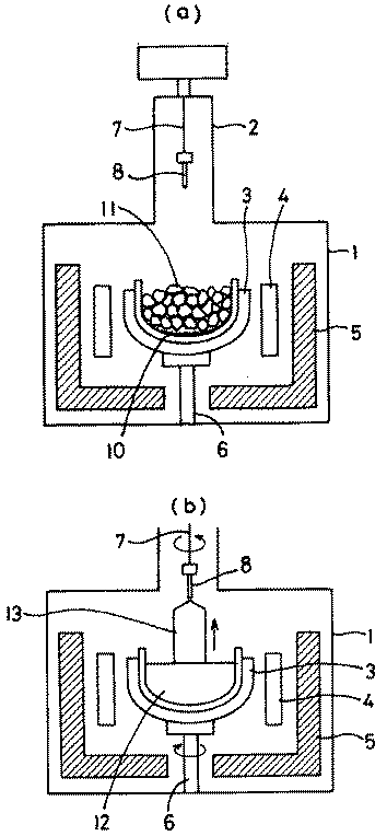
以下に本発明の実施形態を図面に基づいて説明する。図1は本発明の実施形態に係る結晶育成方法の説明図で、(a)は原料溶解工程、(b)は引き上げ工程を示す。
【0029】
結晶育成装置は、メインチャンバ1と、その上面中心部に連結されたプルチャンバ2とを備えている。これらは、軸方向を垂直とした略円筒状の真空容器からなり、図示されない水冷機構を有している。メインチャンバ1の内部には、略中央に位置して坩堝3が配置されると共に、坩堝3の外側に位置してヒータ4及び保温筒5が配置されている。
【0030】
坩堝3は石英製の内層容器と黒鉛製の外層容器とからなり、回転式かつ昇降式の支持軸6により支持されている。坩堝3の上方には、回転式かつ昇降式の引き上げ軸7がプルチャンバ2を通して吊り下げられ、引き上げ軸7の下端には種結晶8が装着されている。
【0031】
結晶成長を行うには先ず、図1(a)に示すように、チャンバを解体した状態で、坩堝3の内底面上に炭素粉末10を投入し、その上からシリコンの多結晶原料11を装填する。炭素粉末10の投入量は、結晶前半部の炭素濃度が1×10¹⁶atoms/cm3 以上となるように調整され、これにより結晶後半部の炭素濃度は5×10¹⁶atoms/cm3 以上となる。
【0032】
原料装填が終わると、チャンバを組み立て、その内部を真空排気した状態でヒータ4を作動させて、坩堝3内の原料を溶解する。このようにして、所定量の炭素がドープされたシリコンの原料融液12を坩堝3内に生成する〔図1(b)参照〕。
【0033】
原料融液12の生成が終わると、図1(b)に示すように、引き上げ軸7の下端に装着された種結晶8を原料融液12に浸漬し、この状態から坩堝3と引き上げ軸7を逆方向に回転させながら引き上げ軸7を上昇させる。これにより、種結晶8の下方にシリコンの単結晶13が育成される。ここにおける引き上げ速度は、OSFリングが結晶の最外周部に生じるか若しくはその外側に消滅する高速度とされる。
【0034】
育成された単結晶13は、1×10¹⁶atoms/cm3 以上の炭素を含むものとなり、その結果、高速引き上げによって育成された単結晶であるにもかかわらず空孔クラスタの発生が抑制された高品質結晶となる。
【0035】
そして、この単結晶13は、高速引き上げによって育成されているので、生産性が高く安価である。加えて、有転位化の危険性が低いので、歩留りが高く、この点からも経済性に優れる。
【0036】
また、炭素ドープのための炭素粉末を坩堝3の内底面上に敷いて原料溶解を行うので、炭素粉末が完全に溶け、その溶け残りによる炭素濃度のバラツキ及び有転位化が防止される。しかも、炭素粉末の飛散が生じないので、飛散粉末の落下による有転位化も防止される。従って、無転位化引き上げ歩留りが一層高い。
【0037】
【実施例】
次に本発明の実施例を示し、従来例と比較することにより、本発明の効果を明らかにする。
【0038】
坩堝の内底面上に種々の量の炭素粉末を投入した。粉末サイズは約1μmである。次に、通常のシリコン多結晶原料100kgを装填し、その後、p型ドーパントとしてボロン−シリコン合金0.6g添加した。このようにして原料の装填を行った後、チャンバ内を10TorrのAr雰囲気にし、ヒータパワーを70kwに設定して、多結晶原料を溶解した。そして、この溶解により生成された原料融液から、100方位の種結晶により直径が8インチのシリコン単結晶を1000mm育成した。このときの結晶成長速度(引き上げ速度)は、OSFリングが結晶の最外周部に発生する0.8mm/分に設定した。
【0039】
比較のために、炭素粉末を投入しない場合、及び多結晶原料の装填後に炭素粉末を投入した場合についても、同様の結晶育成を実施した。炭素粉末を投入しない場合の引き上げ速度は、上述の0.8mm/分(高速引き上げ)と、OSFリングが中心部に発生する0.5mm/分(低速引き上げ)の2種類とした。
【0040】
炭素粉末の投入法及び投入量、無転位引き上げ率、育成結晶のトップから500mmの位置で切り出したサンプルウエーハの炭素濃度及び空孔クラスタ個数を調査した結果を表1に示す。空孔クラスタ個数は、サンプルウエーハを鏡面研磨し、SC1洗浄後パーティクルカウンタにより0.13μm以上の空孔クラスタの個数(COP数)をカウントしたものである。
【0041】
表1から分かるように、原料融液中に炭素が積極的にドープされていない場合は、ウエーハ1枚当たり180個(密度は0.57個/cm2 )の空孔クラスタが発生するが、結晶中の炭素濃度が1×10¹⁶atoms/cm3 以上となるように炭素粉末を投入することにより、空孔クラスタ数は35個以下(密度は0.112個/cm2 以下)に減少する。但し、多結晶原料装填後に炭素粉末を投入した場合は、粉末の溶け残り等のため無転位引き上げ率が低下し、結晶中の炭素濃度も狙い値より低下する。
【0042】
炭素をドープしなくても引き上げ速度を低下させた場合も空孔クラスタの個数はウエーハ1枚当たり25個に減少するが、無転位引き上げ率は20%に低下する。また、速度低下による生産性の低下が大きいことは言うまでもない。
【0043】
【表1】
【発明の効果】
以上の説明から明らかなように、本発明のシリコンウエーハは、空孔クラスタが少ない上に、結晶育成工程で引き上げ速度を低下させずとも製造されるので、低速育成工程を経て製造されたウエーハと比べて安価である。
【0045】
また、本発明の結晶育成方法は、引き上げ速度を低下させずとも空孔クラスタの発生を抑えることができるので、生産性及び無転位歩留りが高い。従って、高品質のウエーハを安価に製造することができる。
【図面の簡単な説明】
【図1】本発明の実施形態に係る結晶成長方法の説明図であり、(a)は原料溶解工程、(b)は引き上げ工程を示す。
【符号の説明】
1 メインチャンバ
2 プルチャンバ
3 坩堝
4 ヒータ
5 保温筒
6 支持軸
7 引き上げ軸
8 種結晶
10 炭素粉末
11 多結晶原料
12 原料融液
13 単結晶[0001]
BACKGROUND OF THE INVENTION
The present invention relates to a silicon wafer used as a material for a semiconductor device and a crystal growth method for manufacturing the wafer.
[0002]
[Prior art]
A silicon wafer used as a material for a semiconductor device is collected mainly from a silicon single crystal grown by a CZ method. As is well known, the CZ method is a method in which a seed crystal is immersed in a silicon raw material melt produced in a quartz crucible, and the seed crystal is pulled up while rotating the seed crystal and the quartz crucible in the opposite direction. This is a method for growing a single crystal.
[0003]
It is known that a silicon wafer manufactured through such a growth process by the CZ method generates a ring-shaped oxidation-induced stacking fault called an OSF ring when subjected to a thermal oxidation treatment. The OSF ring itself not only causes deterioration of the characteristics of the semiconductor device, but also has different physical properties on the outside and inside of the ring, and dislocation clusters are generated outside the OSF ring due to aggregation of interstitial atoms. However, the inside of the OSF ring is relatively healthy. On the other hand, it is known that the OSF ring moves to the outer peripheral side of the single crystal as the pulling speed increases.
[0004]
Under these circumstances, so far, single crystal growth has been performed under high-speed pulling conditions such that the OSF ring is distributed in the outermost peripheral portion of the crystal that is excluded from the effective portion during device formation. From this point, this high-speed pulling is preferable.
[0005]
However, the inside of the OSF ring is not without problems. In this portion, vacancy clusters caused by flocculation are generated. Although this defect appears as a small pit when the wafer surface is etched, it is so small that it has not been particularly regarded as a problem until now. However, since the pattern width has become very fine as the degree of integration has increased significantly in recent years, even these high-quality wafers have become a problem.
[0006]
This vacancy cluster hardly occurs in a so-called epitaxial wafer in which a silicon single crystal thin film is grown on a wafer. However, since this wafer is very expensive, the vacancy cluster is raised by pulling up the single crystal by the CZ method. From this point of view, it is required to grow fewer crystals. From this point of view, in high-grade crystal growth, the pulling speed is slowed and the OSF ring is pulled inside the outermost periphery of the crystal. Thus, a low-speed pulling method is conceived in which the defect portion is concentrated in the central portion or disappears in the central portion to reduce the number of hole clusters.
[0007]
[Problems to be solved by the invention]
However, this low speed raising has a problem that the productivity is remarkably lowered as compared with the high speed raising. Moreover, since the pulling time becomes longer by slowing the pulling speed, the risk of causing dislocation increases, and the yield decreases due to this dislocation.
[0008]
Therefore, the silicon wafer manufactured through the growing process by the low speed pulling is more expensive than that by the high speed pulling.
[0009]
Incidentally, when the OSF ring is generated at a half position in the radial direction of the crystal, it is necessary to pull the OSF ring at a speed about 0.7 times the maximum pulling speed, and the OSF ring disappears at the center of the crystal. In order to do this, it is necessary to raise the speed by about 0.6 times the maximum pulling speed.
[0010]
An object of the present invention is to provide a silicon wafer having a small number of vacancy clusters and a low manufacturing cost.
[0011]
Another object of the present invention is to provide a crystal growth method capable of suppressing the generation of vacancy clusters without reducing the pulling rate.
[0012]
[Means for Solving the Problems]
By the way, in a general silicon single crystal used as a semiconductor device material, carbon is treated as an impurity, and this carbon is usually not included except for the inevitable mixing. There are two types of carbon that are inevitably mixed: those that are included as impurities in the polycrystalline silicon material of silicon, and those that are mixed from the surrounding graphite heater during the growth process of the single crystal. The wafer is 0.5 × 10 16 atoms / cm 3 or less. Further, in some cases, carbon is actively added to strengthen the wafer. However, even in such a carbon-reinforced wafer, the carbon concentration is less than 1 × 10 16 atoms / cm 3 .
[0013]
However, it has become clear from various experimental investigations by the present inventors that when carbon is intentionally added in a large amount, it can be a factor that suppresses the generation of vacancy clusters. Based on this, the present inventors have investigated the influence of the carbon concentration on the vacancy cluster. As a result, when the carbon concentration is 1 × 10 16 atoms / cm 3 or more, the vacancy cluster inside the OSF ring It has been found that the occurrence of water is remarkably suppressed and low speed raising is not required.
[0014]
The reason why the generation of vacancy clusters is suppressed by carbon is not clear at present, but it is thought to be as follows. It is considered that the precipitates resulting from carbon compress and strain the surrounding Si lattice, and vacancies are consumed to alleviate this strain.
[0015]
In order to easily manufacture a wafer to which carbon is positively added, it is necessary to pull up the single crystal from the raw material melt doped with carbon. The present inventors also investigated and studied the method of doping carbon into the raw material melt in the crucible. As a result, the following findings could be obtained.
[0016]
Since carbon has a higher melting point than silicon, the method of adding carbon powder to the raw material melt causes undissolved or scattered carbon, and the carbon concentration of the raw material melt is not accurately controlled. There is a problem that the obtained powder is taken into the single crystal and causes dislocation.
[0017]
In order to solve this problem, the present inventors have studied a method of adding carbon powder. As a result, when the polycrystalline raw material is melted in the crucible to produce a raw material melt, the crucible is charged prior to loading of the polycrystalline raw material. It is found that if carbon powder is laid on the inner bottom surface of the steel, not only the powder is prevented from scattering, but also the carbon powder is efficiently heated by the high temperature crucible bottom, and the powder remains undissolved. did.
[0018]
The silicon wafer of the present invention is a silicon wafer in which an OSF ring is generated in the outermost peripheral portion or disappears outside thereof, and has a carbon concentration of 1 × 10 16 atoms / cm 3 or more and a hole cluster generation region The number of generated pore clusters per unit area of 0.13 μm or more in FIG. 5 is 0.5 or less per cm 2 after one SC1 cleaning.
[0019]
By setting the carbon concentration in the silicon wafer to 1 × 10 16 atoms / cm 3 or more, the generation of vacancy clusters in the vacancy cluster generation region is remarkably suppressed. Also, recent crystal growth tends to make it difficult for oxygen to precipitate due to low oxygen and low temperatures, and as a result, the wafer has reduced the gettering ability due to oxygen precipitates, but the carbon in the crystal precipitates oxygen. Therefore, increasing the carbon concentration is advantageous from the viewpoint of increasing the gettering ability of the wafer.
[0020]
The carbon concentration is preferably 2 × 10 16 atoms / cm 3 or more, particularly preferably 5 × 10 16 atoms / cm 3 or more, from the viewpoint of suppressing the generation of vacancy clusters. However, if the concentration is too high, it causes dislocation, and therefore the upper limit is preferably 5 × 10 17 atoms / cm 3 or less, particularly preferably 2 × 10 17 atoms / cm 3 or less.
[0021]
The hole cluster generation region means the inside of the ring when the OSF ring is generated, and the whole wafer when the OSF ring disappears to the outside. Further, in the case where the OSF ring disappears at the center of the crystal, there is no vacancy cluster generation region.
[0022]
The vacancy clusters appear on the surface of the wafer by etching and can be observed, and the size and number of vacancy clusters that can be observed vary depending on the degree of the treatment. The size and the number of the vacancy clusters referred to in the present invention are those for the vacancy clusters that appear at the stage of one SC1 cleaning. Note that the SC1 cleaning is a pretreatment method widely used for wafer defect inspection, and a typical one is 75 with a SC1 cleaning solution of NH 4 OH: H 2 O 2 : H 2 O = 1: 1: 5. The process which wash | cleans a wafer on the conditions for 20 degreeC * can be mentioned.
[0023]
The number of clusters is 0.5 / cm 2 or less in the present invention, but is preferably 0.1 / cm 2 or less, and particularly preferably 0.03 / cm 2 or less.
[0024]
The crystal growth method of the present invention is a crystal growth method for growing a silicon single crystal using the CZ method. Carbon is doped so that the carbon concentration in the grown crystal is 1 × 10 16 atoms / cm 3 or more. The single crystal is pulled from the silicon melt at a pulling speed at which an OSF ring is generated at the outermost peripheral portion of the crystal or disappears outside the crystal.
[0025]
As a method for producing the raw material melt, a method of charging carbon powder on the inner bottom surface of the crucible and then charging a polycrystalline raw material is preferable.
[0026]
In the present invention, the carbon concentration in the grown crystal is set to 1 × 10 16 atoms / cm 3 or more. If the carbon concentration is less than 1 × 10 16 atoms / cm 3, a carbon concentration of 1 × 10 16 atoms / cm 3 or more cannot be secured. This is because the generation is not sufficiently suppressed. A preferable lower limit is 2 × 10 16 atoms / cm 3 or more, and 5 × 10 16 atoms / cm 3 or more is particularly preferable. Although the upper limit of the carbon concentration is not particularly defined, 5 × 10 17 atoms / cm 3 or less is preferable and 2 × 10 17 atoms / cm 3 or less is particularly preferable because an extremely high concentration causes dislocation.
[0027]
With respect to the pulling speed, in order to increase productivity and suppress a decrease in yield due to dislocations, high-speed pulling in which the OSF ring is generated at the outermost peripheral portion of the crystal or disappears outside is preferable. It is also possible to narrow the generation area of the hole clusters by adopting the low speed pulling generated inside the outermost peripheral part.
[0028]
DETAILED DESCRIPTION OF THE INVENTION
Embodiments of the present invention will be described below with reference to the drawings. FIG. 1 is an explanatory view of a crystal growth method according to an embodiment of the present invention, where (a) shows a raw material melting step and (b) shows a pulling step.
[0029]
The crystal growing apparatus includes a main chamber 1 and a pull chamber 2 connected to the center of the upper surface thereof. These are formed of a substantially cylindrical vacuum vessel whose axial direction is vertical, and has a water cooling mechanism (not shown). Inside the main chamber 1, a
[0030]
The
[0031]
In order to perform crystal growth, first, as shown in FIG. 1A, with the chamber disassembled,
[0032]
When the material loading is completed, the chamber is assembled, the heater 4 is operated in a state where the inside is evacuated, and the material in the
[0033]
When the production of the
[0034]
The grown
[0035]
And since this
[0036]
Further, since carbon powder for carbon doping is spread on the inner bottom surface of the
[0037]
【Example】
Next, examples of the present invention will be shown, and the effects of the present invention will be clarified by comparing with the conventional examples.
[0038]
Various amounts of carbon powder were placed on the inner bottom surface of the crucible. The powder size is about 1 μm. Next, 100 kg of a normal silicon polycrystalline material was charged, and then 0.6 g of a boron-silicon alloy was added as a p-type dopant. After the raw materials were charged in this manner, the polycrystalline raw material was dissolved by setting the interior of the chamber to an Ar atmosphere of 10 Torr and setting the heater power to 70 kW. And from the raw material melt produced | generated by this melt | dissolution, 1000 mm of silicon single crystals with a diameter of 8 inches were grown by 100-direction seed crystals. The crystal growth rate (pull-up rate) at this time was set to 0.8 mm / min at which the OSF ring was generated at the outermost periphery of the crystal.
[0039]
For comparison, the same crystal growth was performed when carbon powder was not added and when carbon powder was charged after the polycrystalline raw material was charged. The pulling speeds when carbon powder was not charged were two types, 0.8 mm / min (high speed pulling) described above and 0.5 mm / min (low speed pulling) at which the OSF ring was generated at the center.
[0040]
Table 1 shows the results of investigating the charging method and amount of carbon powder, the dislocation-free pulling rate, the carbon concentration of the sample wafer cut out at a position 500 mm from the top of the grown crystal, and the number of hole clusters. The number of hole clusters is obtained by mirror-polishing the sample wafer and counting the number of hole clusters (number of COPs) of 0.13 μm or more with a particle counter after SC1 cleaning.
[0041]
As can be seen from Table 1, when carbon is not actively doped in the raw material melt, 180 vacancy clusters are generated per wafer (density is 0.57 / cm 2 ). By introducing carbon powder so that the carbon concentration in the crystal is 1 × 10 16 atoms / cm 3 or more, the number of vacancy clusters is reduced to 35 or less (the density is 0.112 pieces / cm 2 or less). . However, when carbon powder is charged after the polycrystalline raw material is charged, the dislocation-free pulling rate decreases due to undissolved powder and the like, and the carbon concentration in the crystal also decreases from the target value.
[0042]
Even when carbon is not doped, the number of vacancy clusters is reduced to 25 per wafer even when the pulling rate is reduced, but the dislocation-free pulling rate is reduced to 20%. Needless to say, the decrease in productivity due to the decrease in speed is large.
[0043]
[Table 1]
【The invention's effect】
As is clear from the above explanation, the silicon wafer of the present invention has few vacancy clusters and is manufactured without lowering the pulling speed in the crystal growth process. It is cheaper than that.
[0045]
Further, the crystal growth method of the present invention can suppress the generation of vacancy clusters without lowering the pulling rate, so that the productivity and the dislocation yield are high. Therefore, a high quality wafer can be manufactured at low cost.
[Brief description of the drawings]
BRIEF DESCRIPTION OF DRAWINGS FIG. 1 is an explanatory diagram of a crystal growth method according to an embodiment of the present invention, where (a) shows a raw material melting step and (b) shows a pulling step.
[Explanation of symbols]
DESCRIPTION OF SYMBOLS 1 Main chamber 2
Claims (2)
Priority Applications (1)
| Application Number | Priority Date | Filing Date | Title |
|---|---|---|---|
| JP36770297A JP4688984B2 (en) | 1997-12-26 | 1997-12-26 | Silicon wafer and crystal growth method |
Applications Claiming Priority (1)
| Application Number | Priority Date | Filing Date | Title |
|---|---|---|---|
| JP36770297A JP4688984B2 (en) | 1997-12-26 | 1997-12-26 | Silicon wafer and crystal growth method |
Related Child Applications (1)
| Application Number | Title | Priority Date | Filing Date |
|---|---|---|---|
| JP2007335974A Division JP4453756B2 (en) | 2007-12-27 | 2007-12-27 | Crystal growth method |
Publications (2)
| Publication Number | Publication Date |
|---|---|
| JPH11199380A JPH11199380A (en) | 1999-07-27 |
| JP4688984B2 true JP4688984B2 (en) | 2011-05-25 |
Family
ID=18489986
Family Applications (1)
| Application Number | Title | Priority Date | Filing Date |
|---|---|---|---|
| JP36770297A Expired - Fee Related JP4688984B2 (en) | 1997-12-26 | 1997-12-26 | Silicon wafer and crystal growth method |
Country Status (1)
| Country | Link |
|---|---|
| JP (1) | JP4688984B2 (en) |
Families Citing this family (5)
| Publication number | Priority date | Publication date | Assignee | Title |
|---|---|---|---|---|
| JP4012350B2 (en) * | 1999-10-06 | 2007-11-21 | 株式会社ルネサステクノロジ | Semiconductor integrated circuit device and manufacturing method thereof |
| JP2004175620A (en) * | 2002-11-27 | 2004-06-24 | Shin Etsu Handotai Co Ltd | Manufacturing method of single crystal |
| JP4507690B2 (en) * | 2004-05-10 | 2010-07-21 | 信越半導体株式会社 | Silicon single crystal manufacturing method and silicon single crystal |
| JP5104437B2 (en) * | 2008-03-18 | 2012-12-19 | 株式会社Sumco | Carbon doped single crystal manufacturing method |
| JP5136253B2 (en) * | 2008-07-11 | 2013-02-06 | 株式会社Sumco | Method for growing silicon single crystal |
Family Cites Families (6)
| Publication number | Priority date | Publication date | Assignee | Title |
|---|---|---|---|---|
| JPH03183685A (en) * | 1989-12-13 | 1991-08-09 | Nippon Steel Corp | Silicon single crystal rod and production thereof |
| JPH0729878B2 (en) * | 1990-06-07 | 1995-04-05 | 三菱マテリアル株式会社 | Silicon wafer |
| JPH08290995A (en) * | 1995-04-19 | 1996-11-05 | Sumitomo Metal Ind Ltd | Silicon single crystal and method for manufacturing the same |
| US5994761A (en) * | 1997-02-26 | 1999-11-30 | Memc Electronic Materials Spa | Ideal oxygen precipitating silicon wafers and oxygen out-diffusion-less process therefor |
| JPH1192300A (en) * | 1997-09-19 | 1999-04-06 | Nec Corp | Production of semiconductor substrate |
| JP3353681B2 (en) * | 1997-12-26 | 2002-12-03 | 三菱住友シリコン株式会社 | Silicon wafer and crystal growing method |
-
1997
- 1997-12-26 JP JP36770297A patent/JP4688984B2/en not_active Expired - Fee Related
Also Published As
| Publication number | Publication date |
|---|---|
| JPH11199380A (en) | 1999-07-27 |
Similar Documents
| Publication | Publication Date | Title |
|---|---|---|
| TW522456B (en) | Silicon single crystal wafer and method for manufacturing the same | |
| US6517632B2 (en) | Method of fabricating a single crystal ingot and method of fabricating a silicon wafer | |
| JP5515406B2 (en) | Silicon wafer and manufacturing method thereof | |
| KR20000005886A (en) | Silicon Single Crystal Wafer having few defects wherein nitrogen is doped and a method for producing it | |
| JPWO2002002852A1 (en) | Silicon single crystal wafer and its manufacturing method | |
| US6139625A (en) | Method for producing a silicon single crystal wafer and a silicon single crystal wafer | |
| KR100747726B1 (en) | Silicon Wafer and Manufacturing Method Thereof | |
| JP2010222241A (en) | Silicon single crystal wafer for igbt and method for manufacturing silicon single crystal wafer for igbt | |
| KR20020019025A (en) | Silicon wafer and method for producing silicon single crystal | |
| US7323048B2 (en) | Method for producing a single crystal and a single crystal | |
| JP3614019B2 (en) | Manufacturing method of silicon single crystal wafer and silicon single crystal wafer | |
| EP1152074A1 (en) | Silicon single crystal wafer and production method therefor | |
| JP4634553B2 (en) | Silicon single crystal wafer and manufacturing method thereof | |
| KR20020018904A (en) | A Single Crystal Silicon Wafer, Ingot and Methods thereof | |
| JP3353681B2 (en) | Silicon wafer and crystal growing method | |
| JP4688984B2 (en) | Silicon wafer and crystal growth method | |
| JP3719088B2 (en) | Single crystal growth method | |
| WO2004065666A1 (en) | Process for producing p doped silicon single crystal and p doped n type silicon single crystal wafe | |
| JP3612974B2 (en) | Crystal growth method | |
| JP2002198375A (en) | Semiconductor wafer heat treatment method and semiconductor wafer manufactured by the method | |
| JP2004161566A (en) | Method for manufacturing silicon wafer, apparatus for manufacturing the same, and silicon wafer | |
| JP4453756B2 (en) | Crystal growth method | |
| JP4080657B2 (en) | Method for producing silicon single crystal ingot | |
| JPH11236293A (en) | High quality silicon single crystal wafer | |
| JP4016471B2 (en) | Crystal growth method |
Legal Events
| Date | Code | Title | Description |
|---|---|---|---|
| RD05 | Notification of revocation of power of attorney |
Free format text: JAPANESE INTERMEDIATE CODE: A7425 Effective date: 20040722 |
|
| A621 | Written request for application examination |
Free format text: JAPANESE INTERMEDIATE CODE: A621 Effective date: 20040831 |
|
| A977 | Report on retrieval |
Free format text: JAPANESE INTERMEDIATE CODE: A971007 Effective date: 20061030 |
|
| A131 | Notification of reasons for refusal |
Free format text: JAPANESE INTERMEDIATE CODE: A131 Effective date: 20070626 |
|
| RD02 | Notification of acceptance of power of attorney |
Free format text: JAPANESE INTERMEDIATE CODE: A7422 Effective date: 20070807 |
|
| A521 | Written amendment |
Free format text: JAPANESE INTERMEDIATE CODE: A523 Effective date: 20070827 |
|
| A02 | Decision of refusal |
Free format text: JAPANESE INTERMEDIATE CODE: A02 Effective date: 20071030 |
|
| A521 | Written amendment |
Free format text: JAPANESE INTERMEDIATE CODE: A523 Effective date: 20071227 |
|
| A911 | Transfer of reconsideration by examiner before appeal (zenchi) |
Free format text: JAPANESE INTERMEDIATE CODE: A911 Effective date: 20080131 |
|
| A912 | Removal of reconsideration by examiner before appeal (zenchi) |
Free format text: JAPANESE INTERMEDIATE CODE: A912 Effective date: 20080229 |
|
| A01 | Written decision to grant a patent or to grant a registration (utility model) |
Free format text: JAPANESE INTERMEDIATE CODE: A01 |
|
| A61 | First payment of annual fees (during grant procedure) |
Free format text: JAPANESE INTERMEDIATE CODE: A61 Effective date: 20110216 |
|
| R150 | Certificate of patent or registration of utility model |
Free format text: JAPANESE INTERMEDIATE CODE: R150 |
|
| FPAY | Renewal fee payment (event date is renewal date of database) |
Free format text: PAYMENT UNTIL: 20140225 Year of fee payment: 3 |
|
| R250 | Receipt of annual fees |
Free format text: JAPANESE INTERMEDIATE CODE: R250 |
|
| R250 | Receipt of annual fees |
Free format text: JAPANESE INTERMEDIATE CODE: R250 |
|
| R250 | Receipt of annual fees |
Free format text: JAPANESE INTERMEDIATE CODE: R250 |
|
| LAPS | Cancellation because of no payment of annual fees |