JP4680655B2 - Solid-state imaging device and manufacturing method thereof - Google Patents
Solid-state imaging device and manufacturing method thereof Download PDFInfo
- Publication number
- JP4680655B2 JP4680655B2 JP2005106681A JP2005106681A JP4680655B2 JP 4680655 B2 JP4680655 B2 JP 4680655B2 JP 2005106681 A JP2005106681 A JP 2005106681A JP 2005106681 A JP2005106681 A JP 2005106681A JP 4680655 B2 JP4680655 B2 JP 4680655B2
- Authority
- JP
- Japan
- Prior art keywords
- transfer
- transfer electrode
- vertical
- horizontal
- imaging device
- Prior art date
- Legal status (The legal status is an assumption and is not a legal conclusion. Google has not performed a legal analysis and makes no representation as to the accuracy of the status listed.)
- Expired - Fee Related
Links
- 238000003384 imaging method Methods 0.000 title claims description 154
- 238000004519 manufacturing process Methods 0.000 title claims description 60
- 239000011229 interlayer Substances 0.000 claims description 116
- 239000000758 substrate Substances 0.000 claims description 112
- 239000004065 semiconductor Substances 0.000 claims description 110
- 238000000034 method Methods 0.000 claims description 79
- 238000006243 chemical reaction Methods 0.000 claims description 35
- 238000005530 etching Methods 0.000 claims description 33
- 238000000926 separation method Methods 0.000 claims description 26
- 238000000059 patterning Methods 0.000 claims description 13
- 239000004020 conductor Substances 0.000 claims description 6
- 239000011159 matrix material Substances 0.000 claims description 6
- 238000005520 cutting process Methods 0.000 description 53
- 229910021420 polycrystalline silicon Inorganic materials 0.000 description 25
- 229920005591 polysilicon Polymers 0.000 description 25
- 101100115215 Caenorhabditis elegans cul-2 gene Proteins 0.000 description 14
- 238000001020 plasma etching Methods 0.000 description 14
- 230000015572 biosynthetic process Effects 0.000 description 12
- 238000000206 photolithography Methods 0.000 description 12
- 238000004518 low pressure chemical vapour deposition Methods 0.000 description 9
- 230000002093 peripheral effect Effects 0.000 description 7
- 239000007769 metal material Substances 0.000 description 6
- 230000000149 penetrating effect Effects 0.000 description 6
- 238000005498 polishing Methods 0.000 description 5
- 238000010586 diagram Methods 0.000 description 4
- 230000003647 oxidation Effects 0.000 description 4
- 238000007254 oxidation reaction Methods 0.000 description 4
- XUIMIQQOPSSXEZ-UHFFFAOYSA-N Silicon Chemical compound [Si] XUIMIQQOPSSXEZ-UHFFFAOYSA-N 0.000 description 3
- 229910052782 aluminium Inorganic materials 0.000 description 3
- XAGFODPZIPBFFR-UHFFFAOYSA-N aluminium Chemical compound [Al] XAGFODPZIPBFFR-UHFFFAOYSA-N 0.000 description 3
- 229910052710 silicon Inorganic materials 0.000 description 3
- 239000010703 silicon Substances 0.000 description 3
- WFKWXMTUELFFGS-UHFFFAOYSA-N tungsten Chemical compound [W] WFKWXMTUELFFGS-UHFFFAOYSA-N 0.000 description 3
- 229910052721 tungsten Inorganic materials 0.000 description 3
- 239000010937 tungsten Substances 0.000 description 3
- 238000005229 chemical vapour deposition Methods 0.000 description 2
- 238000010924 continuous production Methods 0.000 description 2
- 230000007547 defect Effects 0.000 description 2
- 230000000694 effects Effects 0.000 description 2
- 238000009413 insulation Methods 0.000 description 2
- 239000010410 layer Substances 0.000 description 2
- 150000004767 nitrides Chemical class 0.000 description 2
- 239000003990 capacitor Substances 0.000 description 1
- 238000001444 catalytic combustion detection Methods 0.000 description 1
- 239000012535 impurity Substances 0.000 description 1
- 238000002955 isolation Methods 0.000 description 1
- 230000003287 optical effect Effects 0.000 description 1
- 230000035945 sensitivity Effects 0.000 description 1
- 239000000126 substance Substances 0.000 description 1
Images


Classifications
-
- H—ELECTRICITY
- H01—ELECTRIC ELEMENTS
- H01L—SEMICONDUCTOR DEVICES NOT COVERED BY CLASS H10
- H01L27/00—Devices consisting of a plurality of semiconductor or other solid-state components formed in or on a common substrate
- H01L27/14—Devices consisting of a plurality of semiconductor or other solid-state components formed in or on a common substrate including semiconductor components sensitive to infrared radiation, light, electromagnetic radiation of shorter wavelength or corpuscular radiation and specially adapted either for the conversion of the energy of such radiation into electrical energy or for the control of electrical energy by such radiation
- H01L27/144—Devices controlled by radiation
- H01L27/146—Imager structures
- H01L27/14683—Processes or apparatus peculiar to the manufacture or treatment of these devices or parts thereof
- H01L27/14685—Process for coatings or optical elements
-
- H—ELECTRICITY
- H01—ELECTRIC ELEMENTS
- H01L—SEMICONDUCTOR DEVICES NOT COVERED BY CLASS H10
- H01L27/00—Devices consisting of a plurality of semiconductor or other solid-state components formed in or on a common substrate
- H01L27/14—Devices consisting of a plurality of semiconductor or other solid-state components formed in or on a common substrate including semiconductor components sensitive to infrared radiation, light, electromagnetic radiation of shorter wavelength or corpuscular radiation and specially adapted either for the conversion of the energy of such radiation into electrical energy or for the control of electrical energy by such radiation
- H01L27/144—Devices controlled by radiation
- H01L27/146—Imager structures
- H01L27/148—Charge coupled imagers
- H01L27/14806—Structural or functional details thereof
- H01L27/14812—Special geometry or disposition of pixel-elements, address lines or gate-electrodes
- H01L27/14818—Optical shielding
-
- H—ELECTRICITY
- H01—ELECTRIC ELEMENTS
- H01L—SEMICONDUCTOR DEVICES NOT COVERED BY CLASS H10
- H01L27/00—Devices consisting of a plurality of semiconductor or other solid-state components formed in or on a common substrate
- H01L27/14—Devices consisting of a plurality of semiconductor or other solid-state components formed in or on a common substrate including semiconductor components sensitive to infrared radiation, light, electromagnetic radiation of shorter wavelength or corpuscular radiation and specially adapted either for the conversion of the energy of such radiation into electrical energy or for the control of electrical energy by such radiation
- H01L27/144—Devices controlled by radiation
- H01L27/146—Imager structures
- H01L27/148—Charge coupled imagers
- H01L27/14831—Area CCD imagers
- H01L27/14843—Interline transfer
Description
本発明は、固体撮像装置及びその製造方法に関する。 The present invention relates to a solid-state imaging device and a manufacturing method thereof.
近年、デジタルカメラやデジタルムービーカメラ、更にはカメラ付携帯電話の急速な普及により、固体撮像装置の需要が急速に伸びている。特に最近では、多画素化や動画対応の求めにより、固体撮像装置の高速駆動化が求められている。その一つの解決策として、遮光膜が垂直CCDの転送電極への転送パルスの供給も兼ねるシャント配線構造が知られている(例えば、特許文献1参照。)。 In recent years, with the rapid spread of digital cameras, digital movie cameras, and camera-equipped mobile phones, the demand for solid-state imaging devices has increased rapidly. In particular, recently, due to demands for increasing the number of pixels and moving images, it is required to drive the solid-state imaging device at high speed. One solution is a shunt wiring structure in which the light shielding film also serves as a transfer pulse supply to the transfer electrode of the vertical CCD (see, for example, Patent Document 1).
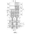
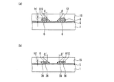
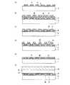
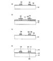
図21〜図29を用いて、シャント配線構造を有する固体撮像装置の一例(従来例1)について説明する。最初に、固体撮像装置の全体構成について説明する。図21は、従来からのシャント配線構造を有する固体撮像装置の全体構成を概略的に示す構成図である。図21に示すように、固体撮像装置は、半導体基板101上の受光領域101aに複数の画素104をマトリックス状に配置して形成されている。半導体基板101としては、例えば、シリコン基板が挙げられる。
An example (conventional example 1) of a solid-state imaging device having a shunt wiring structure will be described with reference to FIGS. First, the overall configuration of the solid-state imaging device will be described. FIG. 21 is a configuration diagram schematically showing an overall configuration of a solid-state imaging device having a conventional shunt wiring structure. As shown in FIG. 21, the solid-state imaging device is formed by arranging a plurality of
また、図21に示す固体撮像装置はインターライン転送を採用しており、各画素は垂直CCD(charge coupled device)102とフォトダイオード(Photo diode)部111とを備えている。半導体基板101には、最終行の垂直CCD102に隣接して水平CCD103が形成されている。水平CCD103の出力端には出力アンプ103bが設けられている。垂直CCD102及び水平CCD103は電荷転送装置として機能する。図21中の矢印は電荷の転送方向を示している。
The solid-state imaging device shown in FIG. 21 employs interline transfer, and each pixel includes a vertical CCD (charge coupled device) 102 and a photodiode (Photo diode)
図21においては図示していないが、垂直CCD102及び水平CCD103それぞれは、転送チャネルと、第1転送電極と、第2転送電極とを備えている。なお、本明細書においては、垂直CCDの転送電極を「垂直転送電極」と称し、水平CCDの転送電極を「水平転送電極」と称する。
Although not shown in FIG. 21, each of the
受光領域101aの周辺領域には、受光領域101aの外縁に沿って垂直バスライン部116が設けられている。垂直バスライン部116は、垂直バスライン配線116a〜116dを備えている。垂直バスライン配線116a〜116dそれぞれには、異なる転送パルスΦV1〜ΦV4が外部から供給されている。水平CCD103における垂直CCD側の反対側(図中下側)には、水平CCD103に沿って、水平バスライン部117が設けられている。水平バスライン部117は、水平バスライン配線117a及び117bを備えている。水平バスライン配線117a及び117bそれぞれには、異なる転送パルスΦH1及びΦH2が外部から供給されている。
In the peripheral area of the
また、垂直CCD102に光が入射しないようにするため、垂直CCD102を列毎に覆うストライプ状の遮光膜113が形成されている。遮光膜113は金属材料で形成されており、垂直バスライン配線116a〜116dのいずれかと接続されている。また、遮光膜113は、コンタクトホール114によって垂直転送電極に接続される。このため、遮光膜113は、垂直CCD102の転送電極へ転送パルスを供給するシャント配線としても機能する。なお、図21においては、遮光膜113の一部を省略している。
Further, in order to prevent light from entering the
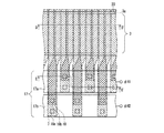
次に、図21に示す固体撮像装置の画素及び垂直CCDの構成について図22を用いて具体的に説明する。図22は、図21に示す固体撮像装置の画素の構成を拡大して示す構成図であり、図22(a)は遮光膜より下層を示し、図22(b)は遮光膜が設けられた状態を示している。 Next, the configuration of the pixels and the vertical CCD of the solid-state imaging device shown in FIG. 21 will be specifically described with reference to FIG. 22 is an enlarged configuration diagram showing the pixel configuration of the solid-state imaging device shown in FIG. 21. FIG. 22A shows a lower layer than the light shielding film, and FIG. 22B shows a light shielding film provided. Indicates the state.
図22(a)に示すように、垂直CCD102は、半導体基板101に形成された転送チャネル102aと、その上に形成された第1垂直転送電極106及び第2垂直転送電極109とを備えている。フォトダイオード部111は、光電変換部111aと、読み出し部111bと、画素分離部111cとを備えている。これらは半導体基板101に形成されている。
As shown in FIG. 22A, the
光電変換部111aは、光が入射すると、信号電荷を生成し、これを蓄積する。読み出し部111bは、光電変換部111aとそれに対応する垂直CCD102との間の領域に形成されており、光電変換部111aに蓄積された電荷の読み出しを行う。読み出された電荷は転送チャネル102aに転送される。画素分離部111cは、光電変換部111aを、隣接する他の光電変換部111aと対応していない垂直CCD102とから電気的に分離している。
When light enters, the
第1垂直転送電極106及び第2垂直転送電極109は、転送チャネル102a、読み出し部111b及び画素分離部111cを覆うように形成されている。図22(a)において、第1垂直転送電極106及び第2垂直転送電極109には、ハッチングを施している。
The first
また、図22(b)に示すように、遮光膜113は、光電変換部111aの上面が開口され、転送チャネル102a、第1垂直転送電極106及び第2垂直転送電極109が遮光されるように形成されている。遮光膜113の開口を通る光のみが光電変換部111aへと入射する。図22(b)の例では、コンタクトホール114は、遮光膜113と第2垂直転送電極109とを接続している。
Further, as shown in FIG. 22B, the
図21及び図22に示した固体撮像装置の動作について説明する。以下の説明においては適宜図21及び図22を参酌する。先ず、半導体基板101の受光領域101aに光学像が結像されると、各フォトダイオード部111の光電変換部111aは、光電変換を行い、光の強さと光の入射時間とに応じた信号電荷を蓄積する。この状態において、第2垂直転送電極109に、垂直バスライン部116及び遮光膜113を通じてハイレベル電圧(10V〜15V)を印加する。これにより、各フォトダイオード部111の光電変換部111aに蓄積された信号電荷は、読み出し部111bを通って、垂直CCD102の転送チャネル102aに転送される。
The operation of the solid-state imaging device shown in FIGS. 21 and 22 will be described. In the following description, FIGS. 21 and 22 are referred to as appropriate. First, when an optical image is formed on the
次に、上記と同様に、垂直バスライン部116及び遮光膜113を通じて、第1垂直転送電極106および第2垂直転送電極109に、ミドルレベル電圧(0V)とローレベル電圧(−5V〜−10V)とを交互に印加する。これにより、信号電荷は、垂直方向に並んだ垂直CCD102を順次転送され、水平CCD103に到達する。
Next, similarly to the above, the middle level voltage (0 V) and the low level voltage (−5 V to −10 V) are applied to the first
その後、水平CCD103の第1水平転送電極(図示せず)及び第2水平転送電極に、水平バスライン部117を介してハイレベル電圧(2V〜5V)とローレベル電圧(0V)とを交互に印加する。これにより、信号電荷は、水平CCD103から出力アンプ103bへと転送される。
Thereafter, a high level voltage (2 V to 5 V) and a low level voltage (0 V) are alternately applied to the first horizontal transfer electrode (not shown) and the second horizontal transfer electrode of the
出力アンプ103bは、信号電荷を電圧に変換し、外部に信号電圧を出力する。このように、光電変換部111aに蓄積された信号電荷は、垂直CCD102によって垂直方向に転送され、水平CCD103によって水平方向に転送された後、外部に出力される。
The
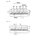
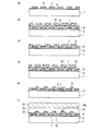
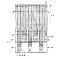
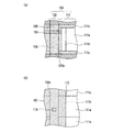
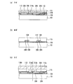
次に、図21に示す従来1の固体撮像装置の垂直CCD及び水平CCDにおける転送電極、遮光膜、バスライン部の構成について図23〜図26を用いて具体的に説明する。先ず、垂直CCDについて説明する。図23は、図21に示す固体撮像装置の垂直CCD及び垂直バスライン部の構成を示す平面図であり、図21中の破線で囲まれた領域Xに対応
している。図24は、図23に示す構成を切断して得られた断面図であり、図24(a)は切断線Q−Q´に沿った断面図、図24(b)は切断線R−R´に沿った断面図、図24(c)は切断線S−S´に沿った断面図である。なお、図24においては、導電性の部材(半導体基板を除く)にのみハッチングを施している。
Next, the configuration of the transfer electrode, the light shielding film, and the bus line portion in the vertical CCD and horizontal CCD of the conventional solid-state imaging device shown in FIG. 21 will be described in detail with reference to FIGS. First, the vertical CCD will be described. FIG. 23 is a plan view showing the configuration of the vertical CCD and the vertical bus line unit of the solid-state imaging device shown in FIG. 21, and corresponds to a region X surrounded by a broken line in FIG. 24 is a cross-sectional view obtained by cutting the configuration shown in FIG. 23. FIG. 24A is a cross-sectional view taken along the cutting line Q-Q ', and FIG. 24B is a cutting line RR. FIG. 24C is a cross-sectional view taken along the cutting line SS ′. In FIG. 24, only conductive members (excluding the semiconductor substrate) are hatched.
図23に示すように、第1垂直転送電極106及び第2垂直転送電極109は、垂直方向に沿って形成された複数の転送チャネル102aを横切るように形成されている。遮光膜113は、転送チャネル102aに沿って、つまり、第1垂直転送電極106及び第2垂直転送電極109を横切るように形成されている。
As shown in FIG. 23, the first
また、第1垂直転送電極106は、コンタクトホール118aによって、垂直バスライン配線116b又は116dに接続されている。第2垂直転送電極109は、コンタクトホール118bによって、垂直バスライン配線116a又は116cに接続されている。遮光膜113は、コンタクトホール114aによって第1垂直転送電極106に接続され、コンタクトホール114bによって第2垂直転送電極109に接続されている。
The first
図24(a)〜(c)に示すように、複数の第1垂直転送電極106は、ゲート絶縁膜105上に、一定の間隔を隔てて形成されている。第1垂直転送電極106の周囲には、第1層間絶縁膜108が形成されている。また、図24(b)及び(c)に示すように、第2垂直転送電極109は、転送チャネル102aが形成されていない領域上では、第1層間絶縁膜108を介して、第1垂直転送電極106の上に形成されている。
As shown in FIGS. 24A to 24C, the plurality of first
一方、図24(a)に示すように、第2垂直転送電極109は、転送チャネル102aが形成された領域上においては、電荷を転送するため、隣り合う第1垂直転送電極106の間のゲート絶縁膜105上に形成されている。但し、第2垂直転送電極109は、その端部109a及び109bが第1垂直転送電極106の端部と重なるように形成されている。
On the other hand, as shown in FIG. 24A, the second
また、図24(a)に示すように、ゲート絶縁膜105、第1垂直転送電極106及び第2垂直転送電極109を被覆するように第2層間絶縁膜112が形成されている。更に、遮光膜113は第2層間絶縁膜112の上に形成されている。遮光膜113と第1垂直転送電極106とを接続する箇所には、第1層間絶縁膜108及び第2層間絶縁膜112を貫通するコンタクトホール114aが形成されている。また、図24には図示していないが、遮光膜113と第2垂直転送電極109とを接続する箇所には、第2層間絶縁膜112を貫通するコンタクトホール114bが形成されている(図23参照)。
Also, as shown in FIG. 24A, a second
また、遮光膜113を被覆するように(遮光膜113が形成されていない領域においては第2層間絶縁膜112を被覆するように)、第3層間絶縁膜115が形成されている。垂直バスライン部116は、第3層間絶縁膜115の上に形成されている。図24(c)に示すように、垂直バスライン配線116b(又は116d)と第1垂直転送電極106とを接続する箇所には、第1層間絶縁膜108、第2層間絶縁膜112及び第3層間絶縁膜115を貫通するコンタクトホール118aが形成されている。垂直バスライン配線116c(又は116a)と第2垂直転送電極109とを接続する箇所には、第2層間絶縁膜112及び第3層間絶縁膜115を貫通するコンタクトホール118bが形成されている。
A third
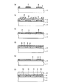
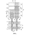
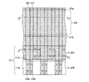
次いで、水平CCDについて説明する。図25は、図21に示す固体撮像装置の水平転送電極、水平バスライン部の構成を具体的に示す平面図である。図26は、図25に示す構成を切断して得られた断面図であり、図26(a)は切断線T−T´に沿った断面図、図26(b)は切断線U−U´に沿った断面図である。なお、図26においては、導電性の部材(半導体基板を除く)にのみハッチングを施している。 Next, the horizontal CCD will be described. FIG. 25 is a plan view specifically showing the configuration of the horizontal transfer electrode and the horizontal bus line portion of the solid-state imaging device shown in FIG. 26 is a cross-sectional view obtained by cutting the configuration shown in FIG. 25. FIG. 26A is a cross-sectional view taken along the cutting line TT ′, and FIG. 26B is a cutting line U-U. It is sectional drawing along '. In FIG. 26, only the conductive members (excluding the semiconductor substrate) are hatched.
図25に示すように、水平CCD103は、水平方向に沿って半導体基板101(図21参照)に設けられた転送チャネル103aと、転送チャネル103aの上にこれを横切るように形成された第1水平転送電極107及び第2水平転送電極110とを備えている。第1水平転送電極107は、コンタクトホール119aによって、水平バスライン配線117a又は117bに接続されている。第2水平転送電極109は、コンタクトホール119bによって、水平バスライン配線117a又は117bに接続されている。
As shown in FIG. 25, the
図26(a)及び(b)に示すように、垂直CCDの場合と同様に(図24参照)、第1水平転送電極107は、ゲート絶縁膜105の上に形成されており、その周囲には第1層間絶縁膜108が形成されている。また、図26(b)に示すように、水平CCD103の転送チャネル103aが形成されていない領域では、第2水平転送電極110は、第1層間絶縁膜108を介して、第1水平転送電極107の上に形成されている。
As shown in FIGS. 26A and 26B, as in the case of the vertical CCD (see FIG. 24), the first
更に、垂直CCDと同様に、図26(a)に示すように、第2水平転送電極110は、転送チャネル103aが形成された領域上では、電荷を転送するため、隣り合う第1水平転送電極107の間のゲート絶縁膜105上に形成されている。また、転送チャネル103aが形成された領域上では、第2水平転送電極110は、その端部110a及び110bが第1水平転送電極107の端部と重なり合うように形成されている。
Further, as in the case of the vertical CCD, as shown in FIG. 26A, the second
また、図26(a)及び(b)に示すように、ゲート絶縁膜105、第1水平転送電極107及び第2水平転送電極110は、第2層間絶縁膜112によって被覆されている。第2層間絶縁膜112は第3層間絶縁膜115によって被覆されている。更に、図26(b)に示すように、第3層間絶縁膜115の上に、金属材料によって、水平バスライン配線117a又は117bが形成されている。
26A and 26B, the
水平バスライン配線117a(又は117b)と第1水平転送電極107とを接続する箇所には、第1層間絶縁膜108、第2層間絶縁膜112及び第3層間絶縁膜115を貫通するコンタクトホール119aが形成されている。また、水平バスライン配線117a(又は117b)と第2水平転送電極109とを接続する箇所には、第2層間絶縁膜112及び第3層間絶縁膜115を貫通するコンタクトホール119bが形成されている。
A
また、図26(a)に示すように、転送チャネル103aが設けられた領域では、第3層間絶縁膜115の上に遮光膜120が形成されている。遮光膜120は、バスライン配線117a及び117bと同じ金属材料によって、同一のプロセスで形成されている。
Further, as shown in FIG. 26A, a
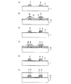
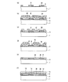
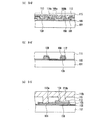
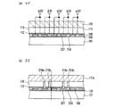
次に、図21〜図26に示した従来例1の固体撮像装置の製造方法について図27〜図29を用いて説明する。図27〜図29は、図21〜図26に示した固体撮像装置の製造方法を示す断面図である。図27(a)〜(d)はそれぞれ主な一連の工程を示している。同様に、図28(a)〜(d)、図29(a)〜(d)もそれぞれ主な一連の工程を示している。また、図27は図24(a)に示した断面図に対応し、図28は図24(b)に示した断面図に対応し、図29は図26(a)に示した断面図に対応する。なお、図27〜図29においては、導電性の部材(半導体基板を除く)とレジストパターンにのみハッチングを施している。 Next, a method for manufacturing the solid-state imaging device of the first conventional example shown in FIGS. 21 to 26 will be described with reference to FIGS. 27 to 29 are cross-sectional views illustrating a method for manufacturing the solid-state imaging device illustrated in FIGS. 21 to 26. 27A to 27D each show a main series of steps. Similarly, FIGS. 28 (a) to 28 (d) and FIGS. 29 (a) to 29 (d) each show a main series of steps. 27 corresponds to the cross-sectional view shown in FIG. 24A, FIG. 28 corresponds to the cross-sectional view shown in FIG. 24B, and FIG. 29 corresponds to the cross-sectional view shown in FIG. Correspond. 27 to 29, only the conductive members (excluding the semiconductor substrate) and the resist pattern are hatched.
最初に、図27(a)、図28(a)及び図29(a)に示すように、例えばシリコン基板などの半導体基板101の表面に、熱酸化法や減圧CVD(化学気相成長)法を利用して、酸化膜や窒化膜等で形成されたゲート絶縁膜105を形成する。その上に、減圧CVD法を利用して、第1垂直転送電極106又は第1水平転送電極107となるポリシリコン膜を形成する。
First, as shown in FIGS. 27A, 28A, and 29A, a thermal oxidation method or a low pressure CVD (chemical vapor deposition) method is performed on the surface of a
次いで、フォトリソグラフィー法及びRIE(反応性イオンエッチング)法を実施し、ポリシリコン膜をパターニング除去する。これにより、第1垂直転送電極106及び第1水平転送電極107が設定された間隔を隔てて形成される。その後、熱酸化法等を実施して、第1垂直転送電極106及び第1水平転送電極107の周囲に第1層間絶縁膜108を形成する。
Next, photolithography and RIE (reactive ion etching) are performed to remove the polysilicon film by patterning. As a result, the first
次に、図27(b)、図28(b)及び図29(b)に示すように、減圧CVD法を利用して、第1垂直転送電極106及び第1水平転送電極107の上に、ポリシリコン膜121を形成する。ポリシリコン膜121は、第2垂直転送電極109及び第2水平転送電極110となる。
Next, as shown in FIGS. 27 (b), 28 (b), and 29 (b), the low-pressure CVD method is used to form the first
次に、図27(c)、図28(c)及び図29((c)に示すように、フォトリソグラフィー法を実施して、第2垂直転送電極109及び第2水平転送電極110の形成領域のみを覆うレジストパターン121を形成する。更に、レジストパターン121をマスクとしてRIE法を実施して、ポリシリコン膜121をパターニング除去する。これにより、第2垂直転送電極109及び第2水平転送電極110が形成される。RIE法の終了後、レジストパターン21を除去する。
Next, as shown in FIGS. 27 (c), 28 (c), and 29 (c), a photolithography method is performed to form regions where the second
その後、図27(d)、図28(d)及び図29(d)に示すように、第2層間絶縁膜112、第3層間絶縁膜115、コンタクトホール114a、114b、119a、119b、遮光膜113を形成する。遮光膜113は、例えば、アルミやタングステンといった金属材料によって形成する。また、図示していないが、コンタクトホール118a及び118b、垂直バスライン配線116a〜116d、水平バスライン配線117a及び117bも形成する。更に、遮光膜120も形成する。これにより、図21〜図26に示した固体撮像装置が得られる。
Thereafter, as shown in FIGS. 27D, 28D, and 29D, the second
このようなシャント配線構造を有する固体撮像装置では、上述したように、第1垂直転送電極106及び第2垂直転送電極109は、コンタクトホール114a又は114bを介して遮光膜113に電気的に接続されている。第1垂直転送電極106及び第2垂直転送電極109には、遮光膜113からも転送パルスが供給される。また、一般的に、転送電極は、比較的抵抗の高いポリシリコン(シート抵抗:約50Ω/□)によって形成されるが、遮光膜113は、アルミ(シート抵抗:0.1Ω/□)やタングステン(シート抵抗:0.5Ω/□)によって形成される。
In the solid-state imaging device having such a shunt wiring structure, as described above, the first
このため、シャント配線構造を有する固体撮像装置を用いれば、シャント配線構造を有さない(ポリシリコンの転送電極のみに転送パルスが印加される)固体撮像装置に比べて、転送パルスの波形なまりを劇的に抑制でき、10倍以上の高速駆動が可能となる。 For this reason, if a solid-state imaging device having a shunt wiring structure is used, the transfer pulse waveform is rounded compared to a solid-state imaging device having no shunt wiring structure (transfer pulses are applied only to polysilicon transfer electrodes). It can be drastically suppressed and a high-speed driving of 10 times or more is possible.
また、シャント配線構造を有する固体撮像装置としては、図21〜図29に示した固体撮像装置(従来例1)以外のものも提案されている(例えば、特許文献2参照)。図30〜図36を用いて、シャント配線構造を有する固体撮像装置の他の例(従来例2)について説明する。先ず、従来例2の垂直CCDについて説明する。 As a solid-state imaging device having a shunt wiring structure, devices other than the solid-state imaging device (conventional example 1) shown in FIGS. 21 to 29 have been proposed (see, for example, Patent Document 2). Another example (conventional example 2) of the solid-state imaging device having the shunt wiring structure will be described with reference to FIGS. First, the vertical CCD of Conventional Example 2 will be described.
図30は、従来からのシャント配線構造を有する固体撮像装置の他の例における垂直転送電極、垂直バスライン部及び遮光膜の構成を示す平面図である。図31は、図30に示す構成を切断線に沿って切断して得られた断面図であり、図31(a)は切断線V−V´に沿った断面図、図31(b)は切断線W−W´に沿った断面図、図31(c)は切断線X−X´に沿った断面図である。なお、図31においても、導電性の部材(半導体基板を除く)にのみハッチングを施している。また、図30及び図31において、従来例1と同様に構成された部分については図23及び図24で示した符号を使用している。 FIG. 30 is a plan view showing a configuration of a vertical transfer electrode, a vertical bus line portion, and a light shielding film in another example of a solid-state imaging device having a conventional shunt wiring structure. 31 is a cross-sectional view obtained by cutting the configuration shown in FIG. 30 along the cutting line. FIG. 31A is a cross-sectional view taken along the cutting line VV ′, and FIG. FIG. 31C is a cross-sectional view taken along the cutting line XX ′. FIG. 31C is a cross-sectional view taken along the cutting line XX ′. In FIG. 31 as well, only the conductive members (excluding the semiconductor substrate) are hatched. In FIGS. 30 and 31, the reference numerals shown in FIGS. 23 and 24 are used for the parts configured in the same manner as in the first conventional example.
図30に示すように、垂直CCD202は、転送チャネル102aと、第1垂直転送電極206及び第2垂直転送電極209とを備えている。従来例2においても、従来例1と同様に、第1垂直転送電極106及び第2垂直転送電極109は、転送チャネル102aを横切るように形成されている。遮光膜113は、転送チャネル102aに沿って形成されている。
As shown in FIG. 30, the
また、従来例1と同様に、第1垂直転送電極206は、コンタクトホール218aによって、垂直バスライン配線116b又は116dに接続されている。第2垂直転送電極209は、コンタクトホール218bによって、垂直バスライン配線116a又は116cに接続されている。遮光膜113は、コンタクトホール214aによって第1垂直転送電極206に接続され、コンタクトホール214bによって第2垂直転送電極209に接続されている。図31(a)〜(c)に示すように、従来例1と同様に、第1垂直転送電極206は、ゲート絶縁膜105上に、一定の間隔を隔てて形成されている。第1垂直転送電極206の周囲には、第1層間絶縁膜108が形成されている。
Similarly to the first conventional example, the first
但し、図30及び図31に示すように、従来例2では、従来例1と異なり、第2垂直転送電極109は、転送チャネル102aが形成されていない領域においても、隣り合う第1垂直転送電極106の間のゲート絶縁膜105上に形成されている。また、第2垂直転送電極109は、転送チャネル102aが形成された領域上において、その端部が第1垂直転送電極106と重なり合わないように形成されている。
However, as shown in FIGS. 30 and 31, in the second conventional example, unlike the first conventional example, the second
なお、図31(a)〜(c)に示すように、従来例1と同様に、第2層間絶縁膜112、遮光膜113、及び第3層間絶縁膜115が形成される(図24参照)。また、コンタクトホール214aは、第1層間絶縁膜108及び第2層間絶縁膜112を貫通する。図31には図示していないが、コンタクトホール214bは、第2層間絶縁膜112を貫通する。更に、図31(c)に示すように、コンタクトホール218aは、第1層間絶縁膜108、第2層間絶縁膜112及び第3層間絶縁膜115を貫通し、コンタクトホール218bは、第2層間絶縁膜112及び第3層間絶縁膜115を貫通する。
As shown in FIGS. 31A to 31C, the second
次に、従来例2の水平CCDについて説明する。図32は、従来からのシャント配線構造を有する固体撮像装置の他の例における水平転送電極、水平バスライン部の構成を示す平面図である。図33は、図32に示す構成を切断線に沿って切断して得られた断面図であり、図33(a)は切断線Y−Y´に沿った断面図、図33(b)は切断線Z−Z´に沿った断面図である。なお、図33においても、導電性の部材(半導体基板を除く)にのみハッチングを施している。また、図32及び図33において、従来例1と同様に構成された部分については図25及び図26で示した符号を使用している。 Next, the horizontal CCD of Conventional Example 2 will be described. FIG. 32 is a plan view showing a configuration of horizontal transfer electrodes and horizontal bus line portions in another example of a solid-state imaging device having a conventional shunt wiring structure. 33 is a cross-sectional view obtained by cutting the configuration shown in FIG. 32 along the cutting line. FIG. 33A is a cross-sectional view taken along the cutting line YY ′, and FIG. It is sectional drawing along the cutting line ZZ '. Also in FIG. 33, only the conductive members (excluding the semiconductor substrate) are hatched. Further, in FIGS. 32 and 33, the reference numerals shown in FIGS. 25 and 26 are used for the parts configured in the same manner as in the first conventional example.
図32に示すように、水平CCD203は、転送チャネル103aと、第1水平転送電極207及び第2水平転送電極210とを備えている。従来例2においても、従来1と同様に、第1水平転送電極207及び第2水平転送電極210は、転送チャネル103aの上にこれを横切るように形成されている。
As shown in FIG. 32, the
また、従来例1と同様に、第1水平転送電極207は、コンタクトホール219aによって、水平バスライン配線117a又は117bに接続されている。第2水平転送電極209は、コンタクトホール219bによって、水平バスライン配線117a又は117bに接続されている。また、第1水平転送電極207は、ゲート絶縁膜105上に、一定の間隔を隔てて形成されている。第1水平転送電極207の周囲には、第1層間絶縁膜108が形成されている。
Similarly to the first conventional example, the first
但し、図33(a)及び(b)に示すように、従来例2では、垂直CCD203の場合と同様に、水平CCD203においても、第2水平転送電極210は、全領域で、隣り合う第1水平転送電極207の間のゲート絶縁膜105上に形成されている。また、第2水平転送電極210は、転送チャネル103aが形成された領域上において、その端部が第1水平転送電極207と重なり合わないように形成されている。よって、転送チャネル103aが形成されていない領域上では、第1水平転送電極207及び第2水平転送電極210の幅は、従来例1の場合よりも狭くなっている。
However, as shown in FIGS. 33A and 33B, in the conventional example 2, as in the case of the
また、従来例1と同様に、第2層間絶縁膜112及び第3層間絶縁膜115が形成されている。第3層間絶縁膜115の上には、水平バスライン配線117a、117b、及び遮光膜120が形成されている。また、図33(b)に示すように、コンタクトホール219aは、第1層間絶縁膜108、第2層間絶縁膜112及び第3層間絶縁膜115を貫通している。コンタクトホール219bは、第2層間絶縁膜112及び第3層間絶縁膜115を貫通している。
Further, as in Conventional Example 1, a second
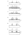
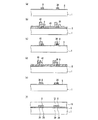
次に、図30〜図33に示した従来例2の固体撮像装置の製造方法について図34〜図36を用いて説明する。図34〜図36は、図30〜図33に示した固体撮像装置の製造方法を示す断面図である。図34(a)〜(f)はそれぞれ主な一連の工程を示している。同様に、図35(a)〜(f)、図36(a)〜(f)もそれぞれ主な一連の工程を示している。また、図34は図31(a)に示した断面図に対応し、図35は図31(b)に示した断面図に対応し、図36は図33(a)に示した断面図に対応する。なお、図34〜図36においては、導電性の部材(半導体基板を除く)とレジストパターンにのみハッチングを施している。 Next, a method of manufacturing the solid-state imaging device of the second conventional example shown in FIGS. 30 to 33 will be described with reference to FIGS. 34 to 36 are cross-sectional views illustrating a method for manufacturing the solid-state imaging device illustrated in FIGS. 30 to 33. FIGS. 34A to 34F show a main series of steps. Similarly, FIGS. 35 (a) to 35 (f) and FIGS. 36 (a) to 36 (f) each show a main series of steps. 34 corresponds to the cross-sectional view shown in FIG. 31A, FIG. 35 corresponds to the cross-sectional view shown in FIG. 31B, and FIG. 36 shows the cross-sectional view shown in FIG. Correspond. 34 to 36, only the conductive members (excluding the semiconductor substrate) and the resist pattern are hatched.
最初に、図34(a)、図35(a)及び図36(a)に示すように、半導体基板101の上に、ゲート絶縁膜105、ポリシリコン膜を順次形成し、フォトリソグラフィー法及びRIE法を実施する。これにより第1垂直転送電極206及び第1水平転送電極207が形成される。その後、第1層間絶縁膜108を形成する。図34(a)、図35(a)及び図36(a)に示す工程は、図27(a)、図28(a)及び図29(a)に示す工程と同様の工程である。
First, as shown in FIGS. 34 (a), 35 (a), and 36 (a), a
次に、図34(b)、図35(b)及び図36(b)に示すように、減圧CVD法を利用して、半導体基板101の上面を覆うように、新たなポリシリコン膜221を形成する。次いで、フォトリソグラフィー法によってレジストパターン222を形成する。レジストパターン222は、半導体基板101の厚み方向において第1層間絶縁膜208と重ならないように形成する。
Next, as shown in FIGS. 34B, 35B, and 36B, a
次に、図34(c)、図35(c)及び図36(c)に示すように、CMP(化学的機械研磨:Chemical Mechanical Polishing)法を実施して、レジストパターン222及びポリシリコン膜221を研磨する。この時、ポリシリコン膜221の研磨レートは、第1層間絶縁膜108の研磨レートに比べて大きく設定されている。よって、第1層間絶縁膜108は研磨されず、ポリシリコン膜221のみが研磨及び除去される。CMPの実施により、第1層間絶縁膜108の上面とポリシリコン膜221の上面とは、連続した平面となる。
Next, as shown in FIGS. 34 (c), 35 (c) and 36 (c), a CMP (Chemical Mechanical Polishing) method is performed to form the resist
次に、図34(d)、図35(d)及び図36(d)に示すように、研磨後のポリシリコン膜221を第2垂直転送電極209及び第2水平転送電極210とするため、フォトリソグラフィー法によってレジストパターン223を形成する。更に、図34(e)、図35(e)及び図36(e)に示すように、レジストパターン223をマスクとしてRIE法を実施する。これにより、ポリシリコン膜221はパターニングされ、第2垂直転送電極209及び第2水平転送電極210が形成される。
Next, as shown in FIGS. 34D, 35D, and 36D, the
その後、図34(f)、図35(f)及び図36(f)に示すように、従来例1と同様に、第2層間絶縁膜112、第3層間絶縁膜115、コンタクトホール214a、214b、219a、219b、遮光膜113及び120を形成する。また、図示していないが、コンタクトホール118a及び118b、垂直バスライン配線116a〜116d、水平バスライン配線117a及び117b、遮光膜120も形成する。これにより、図30〜図33に示した従来例2の固体撮像装置が得られる。従来例2では、従来例1と異なり、CMP法が利用される点で、従来例1と大きく異なる。
上述した従来例1及び従来例2の固体撮像装置は、以下の問題を有している。この点について以下に説明する。 The above-described solid-state imaging devices of Conventional Example 1 and Conventional Example 2 have the following problems. This will be described below.
従来例1の固体撮像装置では、図23及び図24に示すように、第2垂直転送電極109は、転送チャネル102aが形成された領域上では、その端部109a及び109bが第1垂直転送電極106の端部と重なるように形成される。このため、遮光膜113と第1垂直転送電極106とを接続するコンタクトホール114aは、隣り合う第2垂直転送電極109の一方の端部109aと他方の端部109bとの間に形成する必要がある。
In the solid-state imaging device of Conventional Example 1, as shown in FIGS. 23 and 24, the second
しかし、隣り合う第2垂直転送電極109の一方の端部109aと他方の端部109bとの距離は小さく、例えば、画素サイズが3μm角よりも小さくなると、0.6μm未満となる。この場合、コンタクトホール114aは0.3μm角よりも小さく形成しなければならず、その形成は極めて困難になる。
However, the distance between one
更に、隣り合う第2垂直転送電極109の一方の端部109aと他方の端部109bとの距離が小さくなるため、コンタクトホール114aと第2垂直転送電極の端部109a又は109bとの距離も小さくなる。この結果、コンタクトホール114aのホール寸法のばらつきや、コンタクトホール114aおよび第2垂直転送電極109の形成時のマスク合わせのずれ等によって、遮光膜113と第2垂直転送電極109とが接触してショートする場合もある。
Furthermore, since the distance between one
また、上述したように、垂直CCD102の転送チャネル102aが形成された領域上で、第1垂直転送電極106と第2垂直転送電極109とは、互いの端部が重なり合うように形成されており、両者間には層間容量が形成される。また、両者には、それぞれ異なるパルスが印加されるため(図23参照)、この層間容量に起因する消費電力の増加が大きな問題となる。
Further, as described above, the first
同様に、水平CCD103の転送チャネル103aが形成された領域上でも、異なるパルスが印加される第1水平転送電極107と第2水平転送電極110とが、それぞれの端部が互いに重なり合うように形成され(図26(a)参照)、両者には層間容量が形成される。このため、従来例1の固体撮像装置では、水平CCD103においても、この層間容量に起因する消費電力の増加が問題となる。
Similarly, on the region where the
一方、従来例2の固体撮像装置では、図30及び図31に示すように、第2垂直転送電極209は、いずれの領域においても、第1垂直転送電極206に重なっていない。よって、従来例1に比べ、遮光膜113と第1垂直転送電極206とを接続するコンタクトホール214aのホール寸法を大きくできる。従って、例えば、画素サイズが3μm角の場合でも、0.3μm角以上のコンタクトホール214aを形成できる。また、従来例1に比べ、第2垂直転送電極209と遮光膜113とのショートも発生しにくい。
On the other hand, in the solid-state imaging device of Conventional Example 2, as shown in FIGS. 30 and 31, the second
また、従来例2の固体撮像装置では、第1垂直転送電極206と第2垂直転送電極209、第1水平転送電極207と第2水平転送電極210は、互いに重ならないよう形成されているため、従来例1に比べ、層間容量を低減でき、消費電力を低減できる。
In the solid-state imaging device of Conventional Example 2, the first
しかしながら、従来例2の固体撮像装置では、転送電極を重なり合わせないため、垂直バスライン部116が形成される領域において、第1垂直転送電極206及び第2垂直転送電極209の幅(短辺方向の長さ)は、従来例1に比べて小さくなる。同様に、水平バスライン部117が形成される領域においても、第1水平転送電極207及び第2水平転送電極210の幅(短辺方向の長さ)は、従来例1に比べて小さくなる。
However, in the solid-state imaging device of Conventional Example 2, since the transfer electrodes are not overlapped, the widths of the first
このため、垂直転送電極と垂直バスライン部116とを接続するコンタクトホール218a及び218b、水平転送電極と水平バスライン部117とを接続するコンタクトホール219a及び219bのホール寸法を小さくする必要がある。この結果、ホール形成や、水平転送電極207及び210とバスライン配線117a及び117bとのコンタクトが困難となる。
For this reason, the
特に、従来例2のように水平CCD103が2相駆動方式の場合、水平バスライン部217には、1画素当たり4つの水平転送電極207及び210を形成しなければならない。このため、高画素化を図ろうとすると、水平転送電極207及び210の幅(短辺方向の長さ)は非常に小さくなり、コンタクトホール219a及び219bの形成や、水平転送電極207及び210と水平バスライン配線117a及び117bとのコンタクトが非常に困難となる。
In particular, when the
また、固体撮像装置が、全画素読み出し方式を採用する場合は、垂直バスライン部116には、1画素辺り3つ以上の垂直転送電極206及び209を形成しなければならない。このため、垂直CCD102においても、水平CCD103と同様に、垂直転送電極206及び209の幅(短辺方向の長さ)は非常に小さくなる。よって、コンタクトホール218a及び218bの形成や、垂直転送電極206及び209と垂直バスライン配線116a〜116dとのコンタクトも非常に困難となる。
Further, when the solid-state imaging device adopts the all-pixel readout method, three or more
また、従来例2の固体撮像装置の製造は、CMP法を用いるため、図37及び図38に示す問題が発生する。図37は、図30〜図33に示した固体撮像装置の製造方法における一工程のみを示す断面図であり、図37(a)〜(c)は同一工程中の異なる部位の断面を示している。図37(a)は図31(c)に示した断面図に対応し、図37(b)は図31(b)に示した断面図に対応し、図37(c)は図33(a)に示した断面図に対応する。 Also, since the manufacturing of the solid-state imaging device of Conventional Example 2 uses the CMP method, the problems shown in FIGS. 37 and 38 occur. 37 is a cross-sectional view showing only one step in the method of manufacturing the solid-state imaging device shown in FIGS. 30 to 33, and FIGS. 37 (a) to 37 (c) show cross-sections of different parts in the same step. Yes. 37 (a) corresponds to the cross-sectional view shown in FIG. 31 (c), FIG. 37 (b) corresponds to the cross-sectional view shown in FIG. 31 (b), and FIG. This corresponds to the cross-sectional view shown in FIG.
図37に示すように、従来例2の製造方法を利用した場合、第1垂直転送電極206及び第1水平転送電極207のパターンの密度が領域毎に異なるため、CMP後のポリシリコン膜221の膜厚(t1〜t3)にバラツキが発生する。
As shown in FIG. 37, when the manufacturing method of Conventional Example 2 is used, the pattern density of the first
具体的に説明すると、第1水平転送電極207の密度は、第1垂直転送電極206の密度よりも高くなっている。よって、水平CCDの形成領域では、例えば、ポリシリコン膜221の研磨レートよりもレジストパターン222(図34〜図36参照)の研磨レートが速い場合、ポリシリコン膜221の厚みt3は第1層間絶縁膜108の厚みと略同一となる。一方、第1垂直転送電極206の密度は、第1水平転送電極207の密度より低くなっている。このため、垂直CCDの形成領域では、ポリシリコン膜221の厚みt1及びt2は、水平CCDの形成領域におけるポリシリコン膜221よりも薄く形成されてしまう。
More specifically, the density of the first
特に、図37(b)に示すように、フォトダイオード部の周辺領域では、第1垂直転送電極206の密度は最も低いため、ポリシリコン膜221の厚みt2は、更に薄くなる。従って、従来例2においては、第2垂直転送電極209及び第2水平転送電極210における抵抗バラツキが大きくなり、結果、転送パルスの波形なまりが大きくなって、転送効率が低下する恐れがある。また、ポリシリコン膜221の厚みが極端に薄くなった場合は、第2垂直転送電極209及び第2水平転送電極210が断線してしまう恐れもある。
In particular, as shown in FIG. 37B, since the density of the first
図38は、図30〜図33に示した固体撮像装置の製造方法における第2垂直転送電極の形成工程を示す断面図であり、図38(a)及び(b)は連続した工程を示している。従来例2の固体撮像装置の製造工程では、フォトダイオード部の周辺領域において、第1層間絶縁膜108の一方の端部とレジストパターン223の端部とを一致させる必要がある(図35(d)参照)。
FIG. 38 is a cross-sectional view showing the formation process of the second vertical transfer electrode in the method of manufacturing the solid-state imaging device shown in FIGS. 30 to 33, and FIGS. 38 (a) and 38 (b) show the continuous process. Yes. In the manufacturing process of the solid-state imaging device of Conventional Example 2, it is necessary to match one end of the first
しかし、図38(a)に示すように、レジストパターン223が、画素の垂直方向に沿ってずれて形成されてしまうことがある。この状態で、レジストパターン223をマスクとしてRIE法を実施すると、図38(b)に示すように、フォトダイオード部の周辺領域(画素分離部が形成される領域)において第1垂直転送電極206の側壁に、孤立したポリシリコン膜221のエッチング残り224が形成される。この場合、エッチング残り224と第1層間絶縁膜108とで容量が形成され、消費電力が増加してしまう。更に、エッチング残り224を原因として、垂直転送電極間のショートや、画像の黒キズなども発生してしまう。
However, as shown in FIG. 38A, the resist
本発明の目的は、上記問題を解消し、層間容量に起因する消費電力を低減しつつ、配線設計の自由度を高め得る固体撮像装置、及びその製造方法を提供することにある。 An object of the present invention is to provide a solid-state imaging device capable of solving the above-described problems and increasing the degree of freedom in wiring design while reducing power consumption due to interlayer capacitance, and a manufacturing method thereof.
上記目的を達成するために本発明における固体撮像装置は、信号電荷を転送する電荷転送部と、電荷転送部に転送パルスを供給するバスライン部とが設けられた半導体基板を備え、電荷転送部は、前記半導体基板に形成された転送チャネルと、前記転送チャネル上にそれを横切るように設けられた複数の第1転送電極及び複数の第2転送電極と、前記第1転送電極及び前記第2転送電極の上に前記転送チャネルを覆うように形成された遮光膜とを備え、前記バスライン部は、異なる転送パルスを供給する複数のバスライン配線を有し、前記複数のバスライン配線それぞれは、前記複数の第1転送電極及び前記複数の第2転送電極のうちのいずれかと接続されている固体撮像装置であって、前記複数の第1転送電極及び前記複数の第2転送電極は、少なくとも前記バスライン配線が形成される領域に前記半導体基板の厚み方向において重なる領域において、前記第2転送電極が前記第1転送電極の上に位置するように配置され、前記転送チャネルが形成された領域上において、前記第1転送電極と前記第2転送電極とが隣り合うように配置され、前記第2転送電極は、前記転送チャネルが形成された領域上の部分が、少なくとも、異なる転送パルスが印加される前記第1転送電極に、前記半導体基板の厚み方向において重ならないように形成されていることを特徴とする。 In order to achieve the above object, a solid-state imaging device according to the present invention includes a semiconductor substrate provided with a charge transfer unit that transfers a signal charge and a bus line unit that supplies a transfer pulse to the charge transfer unit. Includes a transfer channel formed in the semiconductor substrate, a plurality of first transfer electrodes and a plurality of second transfer electrodes provided on the transfer channel so as to cross the transfer channel, the first transfer electrode, and the second transfer electrode. A light-shielding film formed on the transfer electrode so as to cover the transfer channel, and the bus line section includes a plurality of bus line wirings for supplying different transfer pulses, and each of the plurality of bus line wirings A solid-state imaging device connected to any one of the plurality of first transfer electrodes and the plurality of second transfer electrodes, wherein the plurality of first transfer electrodes and the plurality of second transfer electrodes The second transfer electrode is disposed on the first transfer electrode in a region that overlaps at least the region in which the bus line wiring is formed in the thickness direction of the semiconductor substrate, and the transfer channel is formed. In the region, the first transfer electrode and the second transfer electrode are arranged adjacent to each other, and the second transfer electrode has at least a different transfer pulse at a portion on the region where the transfer channel is formed. The first transfer electrode to which is applied is formed so as not to overlap in the thickness direction of the semiconductor substrate.
また、上記目的を達成するため本発明における固体撮像装置の製造方法は、信号電荷を転送する電荷転送部と、電荷転送部に転送パルスを供給するバスライン部とが設けられた半導体基板を備え、電荷転送部は、前記半導体基板に形成された転送チャネルと、前記転送チャネル上にそれを横切るように設けられた複数の第1転送電極及び複数の第2転送電極とを備える固体撮像装置の製造方法であって、(a)前記半導体基板に前記転送チャネルを形成する工程と、(b)前記半導体基板上に第1導電膜を成膜し、前記第1導電膜をパターニングして前記複数の第1転送電極を形成する工程と、(c)前記第1転送電極の周囲に、前記第1転送電極と前記第2転送電極とを絶縁する第1層間絶縁膜を形成する工程と、(d)前記第1転送電極及び前記半導体基板を覆うように第2導電膜を成膜する工程と、(e)少なくとも前記バスライン配線が形成される領域に前記半導体基板の厚み方向において重なる領域において、前記第1転送電極の上に前記第2導電膜が残存するように前記第2導電膜をパターニングする工程と、(f)前記転送チャネルが形成された領域上において、前記第2導電膜の前記第1層間絶縁膜と前記半導体基板の厚み方向において重なる部分の全部又は一部が開口するようにレジストパターンを形成し、前記レジストパターンをマスクとして等方性エッチングを行って、前記第2転送電極を形成する工程とを有することを特徴とする。 In order to achieve the above object, a method of manufacturing a solid-state imaging device according to the present invention includes a semiconductor substrate provided with a charge transfer unit that transfers signal charges and a bus line unit that supplies transfer pulses to the charge transfer unit. The charge transfer unit includes: a transfer channel formed on the semiconductor substrate; and a plurality of first transfer electrodes and a plurality of second transfer electrodes provided on the transfer channel so as to cross the transfer channel. (A) forming the transfer channel in the semiconductor substrate; (b) forming a first conductive film on the semiconductor substrate; patterning the first conductive film; (C) forming a first interlayer insulating film that insulates the first transfer electrode and the second transfer electrode around the first transfer electrode; d) the first transfer electrode Forming a second conductive film so as to cover the semiconductor substrate, and (e) at least a region of the first transfer electrode in a region overlapping with the bus line wiring in the thickness direction of the semiconductor substrate. Patterning the second conductive film so that the second conductive film remains thereon; and (f) the first interlayer insulating film of the second conductive film on the region where the transfer channel is formed; Forming a resist pattern so as to open all or part of the overlapping portion in the thickness direction of the semiconductor substrate, and performing isotropic etching using the resist pattern as a mask to form the second transfer electrode; It is characterized by having.
以上の特徴により、本発明における固体撮像装置及びその製造方法によれば、転送チャネルが形成された領域において、第2垂直転送電極間の距離を大きくとることができる。よって、第1転送電極に接続するコンタクトホールを形成するための領域を広くできる。また、少なくとも、バスライン配線が形成される領域に半導体基板の厚み方向において重なる領域、即ち、第1転送電極及び第2転送電極をバスライン配線に接続する領域では、第1転送電極と第2転送電極とを上下に配置する。よって、これらの幅が狭くなるのを抑制できる。これらの点から、本発明における固体撮像装置及びその製造方法によれば、配線設計の自由度を高めることができる。 With the above characteristics, according to the solid-state imaging device and the manufacturing method thereof according to the present invention, the distance between the second vertical transfer electrodes can be increased in the region where the transfer channel is formed. Therefore, a region for forming a contact hole connected to the first transfer electrode can be widened. In addition, at least in a region overlapping with the bus line wiring in the thickness direction of the semiconductor substrate, that is, in a region where the first transfer electrode and the second transfer electrode are connected to the bus line wiring, the first transfer electrode and the second transfer electrode The transfer electrodes are arranged above and below. Therefore, it can suppress that these width | variety becomes narrow. From these points, according to the solid-state imaging device and the manufacturing method thereof in the present invention, the degree of freedom in wiring design can be increased.
また、本発明における固体撮像装置及びその製造方法によれば、転送チャネルが形成された領域において、第2転送電極は、少なくとも、異なる転送パルスが供給される第1転送電極には重ならないように形成される。よって、第1転送電極、第2転送電極及びこれらを絶縁する絶縁膜によって形成される層間容量が大きくなるのを抑制でき、消費電力の増加も抑制できる。 Further, according to the solid-state imaging device and the manufacturing method thereof in the present invention, in the region where the transfer channel is formed, the second transfer electrode does not overlap at least the first transfer electrode to which a different transfer pulse is supplied. It is formed. Therefore, an increase in interlayer capacitance formed by the first transfer electrode, the second transfer electrode, and the insulating film that insulates them can be suppressed, and an increase in power consumption can also be suppressed.
本発明における固体撮像装置は、信号電荷を転送する電荷転送部と、電荷転送部に転送パルスを供給するバスライン部とが設けられた半導体基板を備え、電荷転送部は、前記半導体基板に形成された転送チャネルと、前記転送チャネル上にそれを横切るように設けられた複数の第1転送電極及び複数の第2転送電極と、前記第1転送電極及び前記第2転送電極の上に前記転送チャネルを覆うように形成された遮光膜とを備え、前記バスライン部は、異なる転送パルスを供給する複数のバスライン配線を有し、前記複数のバスライン配線それぞれは、前記複数の第1転送電極及び前記複数の第2転送電極のうちのいずれかと接続されている固体撮像装置であって、前記複数の第1転送電極及び前記複数の第2転送電極は、少なくとも前記バスライン配線が形成される領域に前記半導体基板の厚み方向において重なる領域において、前記第2転送電極が前記第1転送電極の上に位置するように配置され、前記転送チャネルが形成された領域上において、前記第1転送電極と前記第2転送電極とが隣り合うように配置され、前記第2転送電極は、前記転送チャネルが形成された領域上の部分が、少なくとも、異なる転送パルスが印加される前記第1転送電極に、前記半導体基板の厚み方向において重ならないように形成されていることを特徴とする。 The solid-state imaging device according to the present invention includes a semiconductor substrate provided with a charge transfer unit that transfers signal charges and a bus line unit that supplies a transfer pulse to the charge transfer unit, and the charge transfer unit is formed on the semiconductor substrate. Transfer channels, a plurality of first transfer electrodes and a plurality of second transfer electrodes provided on and crossing the transfer channel, and the transfer over the first transfer electrodes and the second transfer electrodes. A light-shielding film formed so as to cover the channel, and the bus line section includes a plurality of bus line wirings for supplying different transfer pulses, and each of the plurality of bus line wirings includes the plurality of first transfer lines. A solid-state imaging device connected to any one of an electrode and the plurality of second transfer electrodes, wherein the plurality of first transfer electrodes and the plurality of second transfer electrodes are at least the basula In the region overlapping the region in which the semiconductor wiring is formed in the thickness direction of the semiconductor substrate, the second transfer electrode is disposed on the first transfer electrode, and on the region where the transfer channel is formed. The first transfer electrode and the second transfer electrode are arranged adjacent to each other, and at least a different transfer pulse is applied to the second transfer electrode at a portion on the region where the transfer channel is formed. The first transfer electrode is formed so as not to overlap in the thickness direction of the semiconductor substrate.
また、上記本発明における固体撮像装置は、前記電荷転送部が、前記信号電荷を垂直方向に転送する垂直電荷転送部を含み、前記垂直電荷転送部の前記転送チャネルは、垂直方向に沿って複数設けられ、前記垂直電荷転送部の前記第1転送電極及び前記第2転送電極は、前記垂直電荷転送部の前記複数の転送チャネルを横切るように設けられ、前記垂直電荷転送部の前記第2転送電極は、前記垂直電荷転送部の前記転送チャネルが形成された領域上の部分が、前記垂直電荷転送部の前記第1転送電極に、前記半導体基板の厚み方向において重ならないように形成されている態様とできる。 In the solid-state imaging device according to the present invention, the charge transfer unit includes a vertical charge transfer unit that transfers the signal charge in a vertical direction, and a plurality of transfer channels of the vertical charge transfer unit are provided along the vertical direction. The first transfer electrode and the second transfer electrode of the vertical charge transfer unit are provided across the plurality of transfer channels of the vertical charge transfer unit, and the second transfer of the vertical charge transfer unit The electrode is formed such that a portion of the vertical charge transfer portion on the region where the transfer channel is formed does not overlap the first transfer electrode of the vertical charge transfer portion in the thickness direction of the semiconductor substrate. It can be an embodiment.
また、上記態様においては、前記垂直電荷転送部の前記遮光膜は、前記垂直電荷転送部の前記複数の転送チャネルそれぞれを個別に覆うように形成され、前記遮光膜は、前記転送チャネルが形成された領域上において、コンタクトホールを介して、前記垂直電荷転送部の前記第1転送電極又は前記第2転送電極に接続されていても良い。 In the above aspect, the light shielding film of the vertical charge transfer unit is formed to individually cover each of the plurality of transfer channels of the vertical charge transfer unit, and the light shielding film is formed with the transfer channel. On the other region, it may be connected to the first transfer electrode or the second transfer electrode of the vertical charge transfer section through a contact hole.
上記態様とすれば、垂直電荷転送部(垂直CCD)において、第1転送電極及び第2転送電極のバスライン部と接続する部分の幅を狭めることなく、第1転送電極と遮光膜とを接続するコンタクトホールの形成領域を広くとれる。よって、第1転送電極と遮光膜とを接続するコンタクトホールや、第1転送電極及び第2転送電極とバスライン部とを接続するコンタクトホールの設計の自由度を高めることができる。また、第1転送電極と遮光膜とを接続するコンタクトホールが第2転送電極の端部に接触して、ショートが発生するのも抑制できる。更に、垂直電荷転送部での層間容量を低減できる。 According to the above aspect, in the vertical charge transfer portion (vertical CCD), the first transfer electrode and the light shielding film are connected without reducing the width of the portion of the first transfer electrode and the second transfer electrode connected to the bus line portion. The contact hole forming region to be formed can be widened. Therefore, it is possible to increase the degree of freedom in designing the contact hole that connects the first transfer electrode and the light shielding film, and the contact hole that connects the first transfer electrode and the second transfer electrode and the bus line portion. In addition, it is possible to suppress the occurrence of a short circuit due to the contact hole connecting the first transfer electrode and the light shielding film contacting the end of the second transfer electrode. Furthermore, the interlayer capacitance in the vertical charge transfer portion can be reduced.
また、上記本発明における固体撮像装置においては、前記半導体基板に、入射光を信号電荷に変換する光電変換部が更に設けられ、前記光電変換部が、前記半導体基板上に、垂直方向及び水平方向に沿ってマトリクス状に複数配置されていても良い。この場合は、前記半導体基板に、垂直方向において互いに隣り合う前記光電変換部を分離する画素分離部が形成されており、前記垂直電荷転送部の前記第2転送電極は、前記画素分離部が形成された領域上の部分も、前記垂直電荷転送部の前記第1転送電極に、前記半導体基板の厚み方向において重ならないように形成されているのが好ましい。このようにすることにより、光電変換部の周辺領域の段差を小さくできるため、光電変換部に入射する光の入射角を広げることができ、高感度の画素を得ることができる。 In the solid-state imaging device according to the present invention, a photoelectric conversion unit that converts incident light into signal charges is further provided on the semiconductor substrate, and the photoelectric conversion unit is disposed on the semiconductor substrate in a vertical direction and a horizontal direction. A plurality of them may be arranged in a matrix along the line. In this case, a pixel separation portion that separates the photoelectric conversion portions adjacent to each other in the vertical direction is formed on the semiconductor substrate, and the second transfer electrode of the vertical charge transfer portion is formed by the pixel separation portion. It is preferable that a portion on the formed region is also formed so as not to overlap the first transfer electrode of the vertical charge transfer portion in the thickness direction of the semiconductor substrate. By doing so, the step in the peripheral region of the photoelectric conversion unit can be reduced, so that the incident angle of light incident on the photoelectric conversion unit can be widened, and a highly sensitive pixel can be obtained.
また、上記本発明における固体撮像装置は、前記電荷転送部が、前記信号電荷を前記水平方向に転送する水平電荷転送部を含み、前記水平電荷転送部の前記転送チャネルは、水平方向に沿って設けられ、前記水平電荷転送部の前記第1転送電極及び前記第2転送電極は、前記水平電荷転送部の前記転送チャネルを横切るように設けられ、前記水平電荷転送部の前記第2転送電極は、前記水平電荷転送部の前記転送チャネルが形成された領域上の部分が、少なくとも、異なる転送パルスが印加される前記水平電荷転送部の前記第1転送電極に、前記半導体基板の厚み方向において重ならないように形成されている態様とできる。 In the solid-state imaging device according to the present invention, the charge transfer unit includes a horizontal charge transfer unit that transfers the signal charge in the horizontal direction, and the transfer channel of the horizontal charge transfer unit extends along the horizontal direction. And the first transfer electrode and the second transfer electrode of the horizontal charge transfer unit are provided so as to cross the transfer channel of the horizontal charge transfer unit, and the second transfer electrode of the horizontal charge transfer unit is A portion of the horizontal charge transfer portion on the region where the transfer channel is formed overlaps at least the first transfer electrode of the horizontal charge transfer portion to which a different transfer pulse is applied in the thickness direction of the semiconductor substrate. It can be made the aspect formed so that it may not become.
上記態様とすれば、水平電荷転送部(水平CCD)において、第1転送電極及び第2転送電極のバスライン部と接続する部分の幅が狭められるのを抑制しつつ、高画素化に対応できる。つまり、高画素化により、第1転送電極と第2転送電極のピッチが小さくなった場合でも、第1転送電極及び第2転送電極とバスライン部とを接続するコンタクトホールの設計の自由度を確保できる。更に、水平電荷転送部での層間容量を低減できる。 According to the above aspect, in the horizontal charge transfer portion (horizontal CCD), it is possible to cope with an increase in the number of pixels while suppressing the narrowing of the width of the portion connected to the bus line portion of the first transfer electrode and the second transfer electrode. . That is, even when the pitch between the first transfer electrode and the second transfer electrode is reduced due to the increase in the number of pixels, the degree of freedom in designing the contact hole that connects the first transfer electrode, the second transfer electrode, and the bus line portion is increased. It can be secured. Furthermore, the interlayer capacitance in the horizontal charge transfer section can be reduced.
また、上記態様においては、前記水平電荷転送部の前記第2転送電極における前記転送チャネルが形成された領域上の部分が、異なる転送パルスが印加される前記水平電荷転送部の前記第1転送電極及び同一の転送パルスが印加される前記水平電荷転送の前記第1転送電極に、前記半導体基板の厚み方向において重ならないように、前記水平電荷転送部の前記第2転送電極を形成するのが好ましい。この場合は、水平電荷転送部での層間容量をよりいっそう低減できる。更に、水平電荷転送部の第2転送電極による段差を小さくできるため、その上に導電性の遮光膜が形成された場合において、配線間容量を低減できる。 In the above aspect, a portion of the second transfer electrode of the horizontal charge transfer portion on the region where the transfer channel is formed is applied to the first transfer electrode of the horizontal charge transfer portion to which a different transfer pulse is applied. Preferably, the second transfer electrode of the horizontal charge transfer portion is formed so as not to overlap the first transfer electrode of the horizontal charge transfer to which the same transfer pulse is applied in the thickness direction of the semiconductor substrate. . In this case, the interlayer capacitance in the horizontal charge transfer section can be further reduced. Furthermore, since the step due to the second transfer electrode of the horizontal charge transfer portion can be reduced, the inter-wiring capacitance can be reduced when a conductive light shielding film is formed thereon.
また、本発明における固体撮像装置の製造方法は、信号電荷を転送する電荷転送部と、電荷転送部に転送パルスを供給するバスライン部とが設けられた半導体基板を備え、電荷転送部は、前記半導体基板に形成された転送チャネルと、前記転送チャネル上にそれを横切るように設けられた複数の第1転送電極及び複数の第2転送電極とを備える固体撮像装置の製造方法であって、(a)前記半導体基板に前記転送チャネルを形成する工程と、
(b)前記半導体基板上に第1導電膜を成膜し、前記第1導電膜をパターニングして前記複数の第1転送電極を形成する工程と、(c)前記第1転送電極の周囲に、前記第1転送電極と前記第2転送電極とを絶縁する第1層間絶縁膜を形成する工程と、(d)前記第1転送電極及び前記半導体基板を覆うように第2導電膜を成膜する工程と、(e)少なくとも前記バスライン配線が形成される領域に前記半導体基板の厚み方向において重なる領域において、前記第1転送電極の上に前記第2導電膜が残存するように前記第2導電膜をパターニングする工程と、(f)前記転送チャネルが形成された領域上において、前記第2導電膜の前記第1層間絶縁膜と前記半導体基板の厚み方向において重なる部分の全部又は一部が開口するようにレジストパターンを形成し、前記レジストパターンをマスクとして等方性エッチングを行って、前記第2転送電極を形成する工程とを有することを特徴とする。
The solid-state imaging device manufacturing method according to the present invention includes a semiconductor substrate provided with a charge transfer unit that transfers a signal charge and a bus line unit that supplies a transfer pulse to the charge transfer unit. A method for manufacturing a solid-state imaging device, comprising: a transfer channel formed on the semiconductor substrate; and a plurality of first transfer electrodes and a plurality of second transfer electrodes provided on the transfer channel so as to cross the channel. (A) forming the transfer channel in the semiconductor substrate;
(B) forming a first conductive film on the semiconductor substrate and patterning the first conductive film to form the plurality of first transfer electrodes; and (c) around the first transfer electrode. Forming a first interlayer insulating film that insulates the first transfer electrode and the second transfer electrode; and (d) forming a second conductive film so as to cover the first transfer electrode and the semiconductor substrate. (E) the second conductive film remains on the first transfer electrode in a region that overlaps at least a region where the bus line wiring is formed in the thickness direction of the semiconductor substrate. Patterning the conductive film; and (f) all or part of a portion of the second conductive film overlapping the first interlayer insulating film in the thickness direction of the semiconductor substrate on the region where the transfer channel is formed. Regis to open Forming a pattern, the resist pattern by performing isotropic etching as a mask, characterized by a step of forming the second transfer electrodes.
上記本発明における固体撮像装置の製造方法は、前記(f)の工程を実施した後に、前記(e)の工程を実施して前記第2転送電極を形成する態様とすることができる。この態様によれば、第2転送電極の上面の平坦化を容易に達成でき、段差の少ない構造を得ることができる。 The method for manufacturing a solid-state imaging device according to the present invention may be configured such that after the step (f) is performed, the step (e) is performed to form the second transfer electrode. According to this aspect, it is possible to easily achieve the flattening of the upper surface of the second transfer electrode and to obtain a structure with few steps.
また、上記本発明における固体撮像装置の製造方法は、前記半導体基板に、垂直方向及び水平方向に沿ってマトリクス状配置され、且つ、入射光を信号電荷に変換する複数の光電変換部を形成する工程と、前記半導体基板に、垂直方向において互いに隣り合う前記光電変換部を分離する画素分離部を形成する工程とを更に有し、前記(f)の工程において、前記画素分離部が形成された領域上においても、前記第2導電膜の前記第1層間絶縁膜と前記半導体基板の厚み方向において重なる部分が開口するように前記レジストパターンを形成して、前記等方性エッチングを行う態様とすることもできる。この態様とすれば、得られた固体撮像装置において、光電変換部の周辺領域の段差を小さくできるため、光電変換部に入射する光の入射角を広げることができ、高感度の画素を得ることができる。
請求項7または8に記載の固体撮像装置の製造方法。
In the method of manufacturing a solid-state imaging device according to the present invention, a plurality of photoelectric conversion units that are arranged in a matrix along the vertical direction and the horizontal direction and convert incident light into signal charges are formed on the semiconductor substrate. And a step of forming, on the semiconductor substrate, a pixel separation portion that separates the photoelectric conversion portions adjacent to each other in the vertical direction. In the step (f), the pixel separation portion is formed. Also in the region, the isotropic etching is performed by forming the resist pattern so that a portion overlapping the first interlayer insulating film of the second conductive film in the thickness direction of the semiconductor substrate is opened. You can also. According to this aspect, in the obtained solid-state imaging device, the step in the peripheral region of the photoelectric conversion unit can be reduced, so that the incident angle of light incident on the photoelectric conversion unit can be widened, and a highly sensitive pixel is obtained. Can do.
The manufacturing method of the solid-state imaging device of
更に、上記本発明における固体撮像装置の製造方法は、前記第1転送電極及び前記第2転送電極を覆う第2層間絶縁膜を形成する工程と、前記転送チャネルが形成された領域上において、前記第2層間絶縁膜に、前記第1転送電極又は前記第2転送電極が底面に露出するコンタクトホールを形成する工程と、前記コンタクトホール内に導電性材料を充填し、更に、前記第2層間絶縁膜の上に前記導電性材料の膜を形成する工程と、前記導電性材料の膜をパターニングして前記遮光膜を形成する工程とを更に有する態様とすることもできる。 Furthermore, in the method for manufacturing a solid-state imaging device according to the present invention, a step of forming a second interlayer insulating film covering the first transfer electrode and the second transfer electrode, and a region where the transfer channel is formed, Forming a contact hole in which the first transfer electrode or the second transfer electrode is exposed to the bottom surface in the second interlayer insulating film; filling the contact hole with a conductive material; and further, the second interlayer insulation An embodiment may further include a step of forming the conductive material film on the film and a step of patterning the conductive material film to form the light shielding film.
(実施の形態1)
以下、本発明の実施の形態1における固体撮像装置及び固体撮像装置の製造方法について、図1〜図7を参照しながら説明する。最初に、本実施の形態1における固体撮像装置の構成について図1〜図4を用いて説明する。
(Embodiment 1)
Hereinafter, a solid-state imaging device and a method for manufacturing the solid-state imaging device according to
本実施の形態1における固体撮像装置も、背景技術に示した従来例1及び2に示した固体撮像装置と同様に、半導体基板上の受光領域に複数の画素をマトリクス状に配置して形成されている。また、各画素は、垂直電荷転送部(以下、「垂直CCD」。)と、フォトダイオード部とを備えている。更に、半導体基板には、水平電荷転送部(以下、「水平CCD」。)や、垂直バスライン部及び水平バスライン部も形成されている。 The solid-state imaging device according to the first embodiment is also formed by arranging a plurality of pixels in a matrix in a light receiving region on a semiconductor substrate, similarly to the solid-state imaging devices shown in Conventional Examples 1 and 2 shown in the background art. ing. Each pixel includes a vertical charge transfer unit (hereinafter, “vertical CCD”) and a photodiode unit. Further, a horizontal charge transfer portion (hereinafter referred to as “horizontal CCD”), a vertical bus line portion, and a horizontal bus line portion are also formed on the semiconductor substrate.
また、本実施の形態1においても、固体撮像装置はインターライン転送を採用したインターライン転送CCDである。但し、本発明においては、転送方式は特に限定されるものではなく、固体撮像装置は、フルフレームCCDや、フレーム転送CCDであっても良い。また、固体撮像装置がフルフレームCCDやフレーム転送CCDである場合は、垂直電荷転送部が、入射光を信号電荷に変換する光電変換部として機能する。 Also in the first embodiment, the solid-state imaging device is an interline transfer CCD that employs interline transfer. However, in the present invention, the transfer method is not particularly limited, and the solid-state imaging device may be a full frame CCD or a frame transfer CCD. When the solid-state imaging device is a full frame CCD or a frame transfer CCD, the vertical charge transfer unit functions as a photoelectric conversion unit that converts incident light into signal charges.
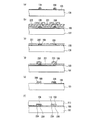
本実施の形態1における固体撮像装置の構成を部分毎に説明する。先ず、本実施の形態1における垂直CCDについて説明する。図1は、本発明の実施の形態1における固体撮像装置の垂直CCD及び垂直バスライン部の構成を示す平面図である。図2は、図1に示す垂直CCD及び垂直バスライン部を切断して得られた断面図であり、図2(a)は切断線A−A´に沿った断面図、図2(b)は切断線B−B´に沿った断面図、図2(c)は切断線C−C´に沿った断面図である。なお、図2においては、導電性の部材(半導体基板を除く)にのみハッチングを施している。
The configuration of the solid-state imaging device according to the first embodiment will be described for each part. First, the vertical CCD in the first embodiment will be described. FIG. 1 is a plan view showing a configuration of a vertical CCD and a vertical bus line unit of the solid-state imaging device according to
図1に示すように、本実施の形態1においても、背景技術に示した従来例1及び2と同様に、垂直CCD2は、垂直方向に沿って形成された複数の転送チャネル2aと、それらを横切るように形成された第1転送電極6及び第2転送電極9とを備えている。転送チャネル2aは、半導体基板1(図2参照)に形成されている。なお、以降の説明においては、垂直CCD2の第1転送電極6は「第1垂直転送電極」6、垂直CCD2の第2転送電極9は「第2水平転送電極」9とする。
As shown in FIG. 1, also in the first embodiment, the
また、図2(a)〜(c)に示すように、第1垂直転送電極6は半導体基板1上のゲート絶縁膜5の上に形成されている。第1垂直転送電極6と第2垂直転送電極9とは、第1層間絶縁膜8によって絶縁されている。転送チャネル2aが形成された領域上においては、第1転送電極6と第2転送電極9とは隣り合うように配置されている。
Further, as shown in FIGS. 2A to 2C, the first
更に、本実施の形態1においても、フォトダイオード部11は、入射光の強さと入射時間とに応じて信号電荷を蓄積する光電変換部11aと、信号電荷の読み出しを行う読み出し部(図1において図示せず(図22(a)参照))と、画素分離部11cとを備えている。第1垂直転送電極6及び第2垂直転送電極9の上には、複数の転送チャネル2aを個別に覆うストライプ状の遮光膜13が形成されている。また、図1及び図2(a)に示すように、遮光膜13は、コンタクトホール14aを介して第1垂直転送電極6に接続され、コンタクトホール14bを介して第2垂直転送電極9に接続されている。
Furthermore, also in the first embodiment, the photodiode unit 11 includes a
また、本実施の形態1においても、垂直バスライン部16は、垂直バスライン配線16a〜16dを備えており、垂直バスライン配線16a〜16dそれぞれには、異なる転送パルスΦV1〜ΦV4が供給されている。また、第1垂直転送電極6は、コンタクトホール18aを介して、垂直バスライン配線16b及び16dに接続されている。第2垂直転送電極9は、コンタクトホール18bを介して、垂直バスライン配線16a及び16bに接続されている。この構成により、第1垂直転送電極6と第2垂直転送電極9とには異なる転送パルスが印加される。
Also in the first embodiment, the vertical
但し、本実施の形態1における固体撮像装置の垂直CCD2及び垂直バスライン部16の構成は、背景技術に示した従来例1及び2と以下の点で異なっている。本実施の形態1では、図1、図2(b)及び(c)に示すように、複数の第1垂直転送電極6及び複数の第2垂直転送電極9は、転送チャネル2aが形成されていない領域上においては、第2垂直転送電極9が第1垂直転送電極6の上に位置するように配置されている。
However, the configurations of the
また、本実施の形態1では、図1及び図2(a)に示すように、第2垂直転送電極9は、転送チャネル2aが形成された領域上の部分が、第1転送電極6に、半導体基板1の厚み方向において重ならないように、即ち、第2垂直転送電極9の端部が第1垂直転送電極6の上へと突き出さないように形成されている。
In the first embodiment, as shown in FIGS. 1 and 2A, the second
このように、本実施の形態1においては、転送チャネル2aが形成された領域上において、第1垂直転送電極6の上には第2垂直転送電極9が存在しないため、コンタクトホール14aの形成領域は、従来例1に比べて広くなっている。例えば、画素サイズが3μm角の場合、垂直CCD2の第1垂直転送電極6の転送方向の長さは1μmを確保することができるため、第1コンタクトホール14aを0.3μm角以上の大きさで容易に形成することができる。
As described above, in the first embodiment, the second
また、転送チャネル2aが形成されていない領域上、具体的には、バスライン配線16a〜16dが形成される領域に半導体基板の厚み方向において重なる領域において、第1垂直転送電極6及び第2垂直転送電極9の幅の制約は小さい。このため、コンタクトホール18a及び18bの形成領域は、従来例2に比べて広くなっている。例えば、画素サイズが3μm角の場合、第1垂直転送電極6及び第2垂直転送電極9における垂直バスライン配線16a〜16dと接触する部分の幅は、1μmを確保することができる。よって、コンタクトホール18a及び18bを0.3μm角以上の大きさで容易に形成することができる。
The first
以上のように、本実施の形態1によれば、従来例1及び2に比べて、垂直CCD2及び水平バスライン部16における設計の自由度を高めることができ、画素の微細化を容易にできる。また、本実施の形態1によれば、従来例1のように第2垂直転送電極9の端部が第1垂直転送電極6と重ならないため、垂直CCD2における垂直転送電極間の層間容量Cを低減できる。よって、従来例1に比べて層間容量Cによる消費電力(=4CV2f)を低減することができる。なお、垂直CCD2において、電圧Vは4V〜10V、好ましくは6V〜8Vに設定される。また、周波数fは1kHz〜100kHz、好ましくは5kHz〜30kHzに設定される。
As described above, according to the first embodiment, the design freedom in the
次に、本実施の形態1における水平CCDについて説明する。図3は、本発明の実施の形態1における固体撮像装置の水平CCD及び水平バスライン部の構成を示す平面図である。図4は、図3に示す水平CCD及び水平バスライン部を切断して得られた断面図であり、図4(a)は切断線D−D´に沿った断面図、図4(b)は切断線E−E´に沿った断面図である。なお、図4においても、導電性の部材(半導体基板を除く)にのみハッチングを施している。
Next, the horizontal CCD in the first embodiment will be described. FIG. 3 is a plan view showing the configuration of the horizontal CCD and the horizontal bus line unit of the solid-state imaging device according to
図3に示すように、本実施の形態1においても、背景技術に示した従来例1及び2と同様に、水平CCD3は、水平方向沿って形成された転送チャネル3aと、これを横切るように形成された第1転送電極7及び第2転送電極9とを備えている。転送チャネル3aも半導体基板1(図4参照)に形成されている。なお、以降の説明においては、水平CCD3の第1転送電極7は「第1水平転送電極」7、水平CCD3の第2転送電極10は「第2水平転送電極」10とする。
As shown in FIG. 3, also in the first embodiment, the
また、後述するように、第1水平転送電極7は、第1垂直転送電極6と同一のプロセスによって形成され、第2水平転送電極10は、第2垂直転送電極9と同一のプロセスによって形成されている。よって、第1水平転送電極7も半導体基板1上のゲート絶縁膜5の上に形成されている。また、第1水平転送電極7と第2水平転送電極10も、第1層間絶縁膜8によって絶縁されている。転送チャネル3aが形成された領域上においては、第1水平転送電極7と第2水平転送電極10とは隣り合うように配置されている。
As will be described later, the first
更に、本実施の形態1においても、水平バスライン部17は、水平バスライン配線17a及び17bを備えており、水平バスライン配線17a及び17bそれぞれには、異なる転送パルスΦH1及びΦH2が供給されている。また、第1水平転送電極7は、コンタクトホール19aを介して水平バスライン配線17a又は17bに接続されている。第2垂直転送電極9はコンタクトホール19bを介して水平バスライン配線17a又は17bに接続されている。
Further, also in the first embodiment, the horizontal
また、隣り合う1本の第1水平転送電極7と1本の第2水平転送電極10とは、一組となって、同一の水平バスライン配線17a又は17bに接続されている。よって、一組となった第1水平転送電極7及び第2水平転送電極10には同一の転送パルスが印加される。一方、隣接するが、組の異なる第1水平転送電極7と第2水平転送電極10とには、それぞれ異なる転送パルスが印加される。
Further, one adjacent first
更に、本実施の形態1においても、図4(a)に示すように、転送チャネル3aが設けられた領域では、第3層間絶縁膜15の上に遮光膜20が形成されている。遮光膜20は、水平バスライン配線17a及び17bと同じ金属材料によって、同一のプロセスで形成されている。
Further, also in the first embodiment, as shown in FIG. 4A, the
但し、本実施の形態1における固体撮像装置の水平CCD3及び水平バスライン部17の構成は、背景技術に示した従来例1及び2と以下の点で異なっている。本実施の形態1では、図3及び図4(b)に示すように、複数の第1水平転送電極7及び複数の第2水平転送電極10は、転送チャネル3aが形成されていない領域上、例えば水平バスライン部17の形成領域においては、第2水平転送電極10が第1水平転送電極7の上に位置するように配置されている。
However, the configurations of the
従って、転送チャネル3aが形成されていない領域上において、第1水平転送電極7及び第2水平転送電極10の幅の制約は小さくなるため、コンタクトホール19a及び19bの形成領域は、従来例2に比べて広くなっている。例えば、画素サイズが3μm角の場合、第1水平転送電極7及び第2水平転送電極10における水平バスライン配線17a又は17bと接触する部分の幅は、1μmを確保することができる。このため、コンタクトホール19a及び19bを0.3μm角以上の大きさで容易に形成することができる。
Accordingly, since the restriction on the width of the first
このことから、本実施の形態1によれば、高画素化により、第1水平転送電極7と第2水平転送電極10のピッチが小さくなった場合でも、従来例2に比べて、水平バスライン部17における設計の自由度を高めることができ、画素の微細化を容易にできる。
Therefore, according to the first embodiment, even when the pitch between the first
また、本実施の形態1では、図3及び図4(a)に示すように、第2水平転送電極10は、転送チャネル3aが形成された領域上の部分が、異なる転送パルスが印加される第1水平転送電極7に、半導体基板1の厚み方向において重ならないように形成されている。即ち、本実施の形態1では、第2垂直転送電極9の端部のうち、同一の水平バスライン配線に接続された第1水平転送電極7側の端部9aのみが、第1水平転送電極7の上へと突き出している。
In the first embodiment, as shown in FIG. 3 and FIG. 4A, the second
このため、本実施の形態1によれば、従来例1に比べて、水平CCD3における水平転送電極間の層間容量Cを低減できる。よって、従来例1に比べて層間容量Cによる消費電力(=2CV2f)を低減でき、ひいては水平CCDの消費電力も低減できる。なお、水平CCD3において、電圧Vは1V〜5V、好ましくは3V程度に設定される。また、周波数fは1kHz〜100kHz、好ましくは10kHz〜40kHzに設定される。
Therefore, according to the first embodiment, the interlayer capacitance C between the horizontal transfer electrodes in the
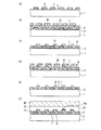
次に、本実施の形態1における固体撮像装置の製造方法について図5〜図7を用いて説明する。図5〜図7は、図1〜図4に示した固体撮像装置の製造方法を示す断面図である。図5(a)〜(f)はそれぞれ主な一連の工程を示している。同様に、図6(a)〜(f)、図7(a)〜(f)もそれぞれ主な一連の工程を示している。また、図5は図2(a)に示した断面図に対応し、図6は図2(b)に示した断面図に対応し、図7は図4(a)に示した断面図に対応する。なお、図5〜図7においては、導電性の部材(半導体基板を除く)とレジストパターンにのみハッチングを施している。 Next, a method for manufacturing the solid-state imaging device according to the first embodiment will be described with reference to FIGS. 5-7 is sectional drawing which shows the manufacturing method of the solid-state imaging device shown in FIGS. 1-4. FIGS. 5A to 5F each show a main series of steps. Similarly, FIGS. 6A to 6F and FIGS. 7A to 7F show a main series of steps. 5 corresponds to the cross-sectional view shown in FIG. 2A, FIG. 6 corresponds to the cross-sectional view shown in FIG. 2B, and FIG. 7 corresponds to the cross-sectional view shown in FIG. Correspond. 5 to 7, only the conductive members (except for the semiconductor substrate) and the resist pattern are hatched.
最初に、例えばシリコン基板などの半導体基板1に不純物をイオン注入して、光電変換部11a(図1参照)、画素分離部11c(図1参照)、転送チャネル2a及び3a(図1及び図3参照)等を形成する。次いで、図5(a)、図6(a)及び図7(a)に示すように、半導体基板1の表面に、熱酸化法や減圧CVD(化学気相成長)法を利用して、酸化膜や窒化膜等で形成されたゲート絶縁膜5を形成する。その上に、減圧CVD法を利用して、ポリシリコン膜等の第1導電膜を形成する。第1導電膜は、第1垂直転送電極6又は第1水平転送電極7となる。
First, impurities are ion-implanted into a
次いで、フォトリソグラフィー法及びRIE(反応性イオンエッチング)法を実施し、第1の導電膜をパターニング除去する。これにより、第1垂直転送電極6及び第1水平転送電極7が、設定された間隔を隔てて形成される。その後、熱酸化法等を実施して、第1垂直転送電極6及び第1水平転送電極7の周囲に第1層間絶縁膜8を形成する。
Next, a photolithography method and an RIE (reactive ion etching) method are performed, and the first conductive film is removed by patterning. As a result, the first
次に、図5(b)、図6(b)及び図7(b)に示すように、減圧CVD法を利用して、第1垂直転送電極6及び第1水平転送電極7の上に、ポリシリコン膜等の第2導電膜21を形成する。第2導電膜21は、第2垂直転送電極9及び第2水平転送電極10となる。
Next, as shown in FIGS. 5B, 6B, and 7B, on the first
次いで、フォトリソグラフィー法を実施して、レジストパターン22を形成する。レジストパターン22は、転送チャネル2a及び3aが形成されていない領域上では、第1垂直転送電極6及び第1水平転送電極7の上方の領域がマスクされるように形成されている(図6(b)参照)。一方、レジストパターン22は、転送チャネル2a及び3aが形成された領域上では、第1垂直転送電極6及び第1水平転送電極7の上方の領域が開口するように形成されている(図5(b)及び図7(b)参照)。
Next, a photolithography method is performed to form a resist
次に、図5(c)、図6(c)及び図7(c)に示すように、レジストパターン22をマスクとして異方性エッチングを行って、第2導電膜21をパターニング除去する。具体的には、RIE法を実施する。これにより、転送チャネル2a及び3aが形成されていない領域上においては、第1垂直転送電極6及び第1水平転送電極7の上にのみ第2導電膜21が残存することになる(図6(c)参照)。また、転送チャネル2a及び3aが形成された領域上においては、第1垂直転送電極6又は第1水平転送電極7の端部と第2導電膜21とが重なった状態となる(図5(c)及び図7(c)参照)。RIE法の終了後、レジストパターン22を除去する。
Next, as shown in FIGS. 5C, 6C, and 7C, anisotropic etching is performed using the resist
次に、図5(d)、図6(d)及び図7(d)に示すように、フォトリソグラフィー法を実施して、レジストパターン23を形成する。レジストパターン23は、垂直CCDの転送チャネル2aが形成された領域上においては、第2導電膜21における、第1層間絶縁膜8(第1垂直転送電極6)と半導体基板1の厚み方向において重なる部分が開口されるように形成されている(図5(d)参照)。
Next, as shown in FIGS. 5D, 6D, and 7D, a photolithography method is performed to form a resist
また、レジストパターン23は、水平CCDの転送チャネル3aが形成された領域上においては、第2導電膜21における、第1層間絶縁膜8(第1水平転送電極7)と半導体基板1の厚み方向において重なる部分の一部が開口されるように形成されている(図7(d)参照。)。本例では、レジストパターン23は、第1水平転送電極7における、同一の水平バスライン配線に接続されていない第2導電膜21側の端部上面を開口している。
The resist
次いで、レジストパターン23をマスクとして等方性エッチングを行う。このとき、第2導電膜21のエッチングは、レジストパターン23の開口部の下方だけでなく、横にも進行するため、第2導電膜21の上面は、第1層間絶縁膜8の上面と略一致するようになる。そして、レジストパターン23を除去する。この結果、図5(e)、図6(e)及び図7(e)に示すように第2垂直転送電極9と第2水平転送電極10とが同時に形成される。
Next, isotropic etching is performed using the resist
その後、図5(f)、図6(f)及び図7(f)に示すように、第2層間絶縁膜12、第3層間絶縁膜15、コンタクトホール14a、14b、19a、19b、遮光膜13を形成する。遮光膜13は、例えば、アルミやタングステンといった金属材料によって形成する。また、図示していないが、コンタクトホール18a及び18b、垂直バスライン配線16a〜16d、水平バスライン配線17a及び17bも形成する。更に遮光膜20も形成する。これにより、図1〜図4に示した固体撮像装置が得られる。
Thereafter, as shown in FIGS. 5 (f), 6 (f) and 7 (f), the second
このように、本実施の形態1における固体撮像装置の製造方法を実施すれば、図1〜図4に示した本実施の形態1における固体撮像装置を得ることができる。また、本実施の形態1における固体撮像装置の製造方法によれば、従来例2のようにCMP法を実施しないで、第1垂直転送電極6に重なる第2垂直転送電極9の端部と、第1水平転送電極7に重なる第2水平転送電極10の端部とを除去できる。このため、従来例2のように、第1垂直転送電極6及び第1水平転送電極7のパターンの粗密によって、第2導電膜21の厚みがばらつくのを抑制でき、膜厚の安定した第2垂直転送電極9及び第2水平転送電極10を得ることができる。よって、本実施の形態1によれば、第2垂直転送電極9及び第2水平転送電極10における抵抗バラツキが大きくなって、消費電力が増加するのを抑制できる。
Thus, if the manufacturing method of the solid-state imaging device in this
なお、本実施の形態1では、垂直CCD2及び水平CCD3の両方において、第1転送電極と第2転送電極とが半導体基板1の厚み方向において重ならないようになっているが、これに限定されるものではない。垂直CCD及び水平CCDのどちらか一方においてのみ、第1転送電極と第2転送電極とが半導体基板の厚み方向において重ならないようになった態様であっても良い。
In the first embodiment, in both the
例えば、第1垂直転送電極6に接続するコンタクトホール14aの形成を容易することのみを目的とするならば、第1垂直転送電極6と第2垂直転送電極9との重なりだけを除去すれば良い。また、水平CCD3の消費電力の低減のみを目的とする場合は、第1水平転送電極7と第2水平転送電極10との重なりだけを除去すれば良い。このような両態様は必要に応じてそれぞれ独立に選択できる。
For example, if the purpose is to facilitate the formation of the
(実施の形態2)
次に、本発明の実施の形態2における固体撮像装置及び固体撮像装置の製造方法について、図8〜図12を参照しながら説明する。本実施の形態2における固体撮像装置は、図1〜図4に示した実施の形態1の固体撮像装置と同様の構成を有している。但し、本実施の形態2における固体撮像装置の製造方法は、以下の点で実施の形態1と異なっている。
(Embodiment 2)
Next, a solid-state imaging device and a method for manufacturing the solid-state imaging device according to
図8〜図10を用いて本実施の形態2における固体撮像装置の製造方法について説明する。図8〜図10は、実施の形態2における固体撮像装置の製造方法を示す断面図である。図8(a)〜(f)はそれぞれ主な一連の工程を示している。同様に、図9(a)〜(f)、図10(a)〜(f)もそれぞれ主な一連の工程を示している。また、図8は図2(a)に示した断面図に対応し、図9は図2(b)に示した断面図に対応し、図10は図4(a)に示した断面図に対応する。なお、図8〜図10においても、導電性の部材(半導体基板を除く)とレジストパターンにのみハッチングを施している。 A method for manufacturing the solid-state imaging device according to the second embodiment will be described with reference to FIGS. 8 to 10 are cross-sectional views illustrating the method for manufacturing the solid-state imaging device according to the second embodiment. 8A to 8F each show a main series of steps. Similarly, FIGS. 9 (a) to 9 (f) and FIGS. 10 (a) to 10 (f) show the main series of steps. 8 corresponds to the cross-sectional view shown in FIG. 2 (a), FIG. 9 corresponds to the cross-sectional view shown in FIG. 2 (b), and FIG. 10 corresponds to the cross-sectional view shown in FIG. Correspond. 8 to 10, only the conductive members (excluding the semiconductor substrate) and the resist pattern are hatched.
最初に、図8(a)、図9(a)及び図10(a)に示すように、転送チャネル2a及び3a(図1及び図3参照)等が形成された半導体基板1上に、ゲート絶縁膜5、第1垂直転送電極6、第1水平転送電極7、及び第1層間絶縁膜8を形成する。なお、図8(a)、図9(a)及び図10(a)に示す工程は、実施の形態1において図5(a)、図6(a)及び図7(a)に示した工程と同様に行われる。
First, as shown in FIGS. 8A, 9A, and 10A, a gate is formed on a
次に、図8(b)、図9(b)及び図10(b)に示すように、減圧CVD法を利用して、第1垂直転送電極6及び第1水平転送電極7の上に、第2導電膜21を形成する。次いで、フォトリソグラフィー法を実施して、レジストパターン24を形成する。レジストパターン24は、実施の形態1において図5(d)、図6(d)及び図7(d)に示したレジストパターン23と同様のものである。
Next, as shown in FIGS. 8B, 9B, and 10B, using the low pressure CVD method, on the first
具体的には、レジストパターン24も、垂直CCDの転送チャネル2aが形成された領域上においては、第2導電膜21における、第1層間絶縁膜8(第1垂直転送電極6)と半導体基板1の厚み方向において重なる部分が開口されるように形成されている(図8(b)参照)。
Specifically, the resist
また、図10(b)に示すように、レジストパターン24は、水平CCDの転送チャネル3aが形成された領域上においては、第2導電膜21における、第1層間絶縁膜8(第1水平転送電極7)と半導体基板1の厚み方向において重なる部分の一部が開口されるように形成されている。図10(b)の例でも、図7(d)の例と同様に、レジストパターン24は、第1水平転送電極7における、同一の水平バスライン配線に接続されていない第2導電膜21側の端部上面を開口している。
Further, as shown in FIG. 10B, the resist
次いで、図8(c)、図9(c)及び図10(c)に示すように、レジストパターン24をマスクとして等方性エッチングを行う。このときも、実施の形態1において図5(d)及び図7(d)に示した工程と同様に、第2導電膜21のエッチングは、レジストパターン24の開口部の下方だけでなく、横にも進行する。よって、第2導電膜21の上面は、第1層間絶縁膜8の上面と略一致するようになる。そして、レジストパターン23を除去する。
Next, as shown in FIGS. 8C, 9C, and 10C, isotropic etching is performed using the resist
次に、図8(d)、図9(d)及び図10(d)に示すように、フォトリソグラフィー法を実施して、レジストパターン25を形成する。レジストパターン25は、実施の形態1において図5(b)、図6(b)及び図7(b)に示したレジストパターン22と同様に、転送チャネル2a及び3aが形成されていない領域上では、第1垂直転送電極6及び第1水平転送電極7の上方の領域がマスクされるように形成されている(図9(d)参照)。
Next, as shown in FIGS. 8D, 9D, and 10D, a photolithography method is performed to form a resist
なお、レジストパターン25は、転送チャネル2aが形成された領域では、当該領域及びその周辺全部を覆うように形成されている(図8(d)参照)。また、レジストパターン25は、転送チャネル3aが形成された領域上では、第2導電膜21の第1垂直転送電極6に重なった部分の一部が開口するように形成されている(図10(d)参照)。
The resist
次いで、レジストパターン25をマスクとして異方性エッチングを行って、第2導電膜21をパターニング除去する。具体的には、RIE法を実施する。そして、レジストパターン25を除去する。この結果、図8(e)、図9(e)及び図10(e)に示すように第2垂直転送電極9と第2水平転送電極10とが同時に形成される。
Next, anisotropic etching is performed using the resist
その後、図8(f)、図9(f)及び図10(f)に示す工程を実施すれば、本実施の形態2においても、実施の形態1において図1〜図4に示した固体撮像装置が得られる。なお、図8(f)、図9(f)及び図10(f)に示す工程は、図5(f)、図6(f)及び図7(f)に示す工程と同様に行われる。 Thereafter, by performing the steps shown in FIGS. 8 (f), 9 (f), and 10 (f), the solid-state imaging shown in FIGS. A device is obtained. 8 (f), FIG. 9 (f) and FIG. 10 (f) are performed in the same manner as the steps shown in FIG. 5 (f), FIG. 6 (f) and FIG. 7 (f).
このように、本実施の形態2における固体撮像装置の製造方法は、等方性エッチングを行った後に異方性エッチングを行うことによって、第2垂直転送電極7及び第2水平転送電極10を形成しており、この点で、実施の形態1における固体撮像装置の製造方法と異なっている。つまり、本実施の形態2においては、背景技術において図24(a)に示した第2垂直転送電極109の端部109aや第2水平転送電極110の端部110aに相当する第2導電膜21の一部を先に除去する。その後、第2導電膜21に対して最終的なパターニングが行われる。
As described above, the manufacturing method of the solid-state imaging device according to the second embodiment forms the second
このため、本実施の形態2における固体撮像装置の製造方法を用いれば、実施の形態1において説明した効果の他に、更に優れた効果を得ることができる。この点について、図11及び図12を用いて説明する。図11は、実施の形態1において図5(d)に示した工程を詳細に示す断面図であり、図11(a)及び(b)は等方性エッチングの前後をそれぞれ示している。図12は、実施の形態2において図8(b)に示した工程を詳細に示す断面図であり、図12(a)及び(b)は等方性エッチングの前後をそれぞれ示している。なお、図11及び図12においては、導電性の部材(半導体基板を除く)にのみハッチングを施している。また、図11及び図12中の破線はエッチングの進行を概念的に示している。 For this reason, if the manufacturing method of the solid-state imaging device according to the second embodiment is used, in addition to the effects described in the first embodiment, further excellent effects can be obtained. This point will be described with reference to FIGS. 11 is a cross-sectional view showing in detail the process shown in FIG. 5D in the first embodiment, and FIGS. 11A and 11B respectively show before and after isotropic etching. 12 is a cross-sectional view showing in detail the process shown in FIG. 8B in the second embodiment, and FIGS. 12A and 12B respectively show before and after isotropic etching. In FIGS. 11 and 12, only conductive members (excluding the semiconductor substrate) are hatched. Also, the broken lines in FIGS. 11 and 12 conceptually show the progress of etching.
図11(a)に示すように、実施の形態1において、レジストパターン23をマスクとして等方性エッチングを行うと、第2導電膜21は、上方向と横方向との二方向から同時にエッチングされる。よって、図11(b)に示すように、実施の形態1においては、第2導電膜21の第1垂直転送電極6と重なる部分が完全に除去されていても、レジストパターン23と第2導電膜21との境界付近に僅かな突起21aが残存してしまう場合がある。
As shown in FIG. 11A, in the first embodiment, when isotropic etching is performed using the resist
それに対して、図12(a)に示すように、実施の形態2においては、第1層間絶縁膜8の上面全体が第2導電膜21によって被覆された状態で等方性エッチングが行われる。よって、第2導電膜21は、先ず、上方向からエッチングされ、その後、上方向と横方向との二方向からエッチングされる。このため、第2導電膜21の第1垂直転送電極6と重なる部分が完全に除去されたときに、図11(b)に示すような突起21aは形成され難く、第2垂直転送電極9の上面は略平坦となり、第1層間絶縁膜8の上面と一致する。このことから、本実施の形態2によれば、実施の形態1に比べ、段差の少ない転送電極を形成することができる。
On the other hand, as shown in FIG. 12A, in the second embodiment, isotropic etching is performed in a state where the entire upper surface of the first
(実施の形態3)
次に、本発明の実施の形態3における固体撮像装置及び固体撮像装置の製造方法について、図13〜図20を参照しながら説明する。最初に、本実施の形態3における固体撮像装置の構成について図13〜図17を用いて説明する。
(Embodiment 3)
Next, a solid-state imaging device and a method for manufacturing the solid-state imaging device according to
本実施の形態3における固体撮像装置は、第1垂直転送電極、第2垂直転送電極、第1水平転送電極、及び第2水平転送電極の構造において、実施の形態1における固体撮像装置と異なっている。但し、本実施の形態3における固体撮像装置は、それ以外の点については、実施の形態1における固体撮像装置と同様に構成されている。 The solid-state imaging device according to the third embodiment is different from the solid-state imaging device according to the first embodiment in the structure of the first vertical transfer electrode, the second vertical transfer electrode, the first horizontal transfer electrode, and the second horizontal transfer electrode. Yes. However, the solid-state imaging device according to the third embodiment is configured in the same manner as the solid-state imaging device according to the first embodiment with respect to other points.
本実施の形態3における固体撮像装置の構成を部分毎に説明する。先ず、本実施の形態3における垂直CCDについて説明する。図13は、本発明の実施の形態3における固体撮像装置の垂直CCD及び垂直バスライン部の構成を示す平面図である。図14は、図13に示す垂直CCD及び垂直バスライン部を切断して得られた断面図であり、図14(a)は切断線F−F´に沿った断面図、図14(b)は切断線G−G´に沿った断面図、図14(c)は切断線H−H´に沿った断面図である。なお、図14においても、導電性の部材(半導体基板を除く)にのみハッチングを施している。
The configuration of the solid-state imaging device according to the third embodiment will be described for each part. First, the vertical CCD according to the third embodiment will be described. FIG. 13 is a plan view showing the configuration of the vertical CCD and the vertical bus line unit of the solid-state imaging device according to
図13及び図14(a)に示すように、本実施の形態3においても、実施の形態1と同様に、第2垂直転送電極39は、転送チャネル2aが形成された領域上の部分が、第1垂直転送電極36に、半導体基板1の厚み方向において重ならないように形成されている。また、図13及び図14(c)に示すように、本実施の形態3においても、実施の形態1と同様に、第1垂直転送電極36及び第2垂直転送電極39は、垂直バスライン部16が形成される領域においては、第2垂直転送電極39が第1垂直転送電極36の上に位置するように配置されている。
As shown in FIGS. 13 and 14A, also in the third embodiment, as in the first embodiment, the second
このため、本実施の形態3における固体撮像装置においても、実施の形態1と同様に、従来例1及び2に比べて、垂直CCD2及び水平バスライン部16における設計の自由度を高めることができ、画素の微細化を容易にできる。また、本実施の形態1と同様に、垂直CCD2における垂直転送電極間の層間容量Cを低減できるため、垂直CCD2の消費電力の低減を図ることができる。
For this reason, in the solid-state imaging device according to the third embodiment, as in the first embodiment, the design freedom in the
但し、図13、図14(b)に示すように、本実施の形態3では、実施の形態1と異なり、第2垂直転送電極39は、画素分離部11cが形成された領域上の部分も、第1垂直転送電極36に、半導体基板1の厚み方向において重ならないように形成されている。本実施の形態3では、第2垂直転送電極9が第1垂直転送電極6の上に配置されるのは、バスライン配線16a〜16dが形成される領域と半導体基板の厚み方向において重なる領域、及びその近傍の領域のみである。
However, as shown in FIGS. 13 and 14B, in the third embodiment, unlike the first embodiment, the second
このため、本実施の形態3によれば、図14(b)に示すように、画素分離部11cが形成された領域上において、第1垂直転送電極36と、第2垂直転送電極39とによる段差を、実施の形態1に比べて小さくできる。この点について図15を用いて説明する。
Therefore, according to the third embodiment, as shown in FIG. 14B, the first
図15は、実施の形態1及び実施の形態2における画素分離部の断面構造を示す断面図であり、図15(a)は実施の形態1の固体撮像装置の画素分離部の断面構造を示す断面図、図15(b)は実施の形態2の固体撮像装置の画素分離部の断面構造を示す断面図である。なお、図15(a)は図2(b)に対応し、図15(b)は図14(b)に対応している。また、図15においても、導電性の部材(半導体基板を除く)にのみハッチングを施している。 FIG. 15 is a cross-sectional view showing a cross-sectional structure of the pixel separation portion in the first and second embodiments, and FIG. 15A shows a cross-sectional structure of the pixel separation portion of the solid-state imaging device of the first embodiment. FIG. 15B is a cross-sectional view showing the cross-sectional structure of the pixel separation portion of the solid-state imaging device according to the second embodiment. FIG. 15A corresponds to FIG. 2B, and FIG. 15B corresponds to FIG. 14B. Also in FIG. 15, only the conductive members (except for the semiconductor substrate) are hatched.
図15(a)に示すように、実施の形態1においては、第2垂直転送電極9は、画素分離部11cが形成された領域上の部分が第1垂直転送電極6の上に位置するように形成されている。これに対して、図15(a)に示すように、実施の形態3においては、第2垂直転送電極9は、画素分離部11cが形成された領域上の部分が第1垂直転送電極6に重ならないように形成されている。このため、実施の形態3における段差の高さh2は、実施の形態1における段差の高さh1よりも低くなる。つまり、実施の形態3によれば、光電変換部11a(図1及び図13参照)の周辺の領域の段差を小さくできる。
As shown in FIG. 15A, in the first embodiment, the second
このため、図15(a)及び(b)に示すように、実施の形態3において光電変換部11aに集光できる光の入射角度θ´は、実施の形態1において光電変換部11aに集光できる光の入射角度θに比べて大きくなる。よって、実施の形態3によれば、実施の形態1に比べて、画素の感度を向上することができる。
For this reason, as shown in FIGS. 15A and 15B, the incident angle θ ′ of the light that can be condensed on the
また、光電変換部11a(図1及び図13参照)の周辺の領域の段差を小さくできるため、遮光膜13が複数の短冊状部分で構成されている場合(図1、図13、図21参照)は、隣り合う短冊状部分間に隙間を形成するのが容易となる。このため、遮光膜13においてショートが発生するのを抑制することもできる。
Moreover, since the level | step difference of the peripheral area | region of the
次に、本実施の形態3における水平CCDについて説明する。図16は、本発明の実施の形態3における固体撮像装置の水平CCD及び水平バスライン部の構成を示す平面図である。図17は、図16に示す水平CCD及び水平バスライン部を切断して得られた断面図であり、図16(a)は切断線I−I´に沿った断面図、図16(b)は切断線J−J´に沿った断面図である。なお、図16においても、導電性の部材(半導体基板を除く)にのみハッチングを施している。
Next, the horizontal CCD in the third embodiment will be described. FIG. 16 is a plan view showing the configuration of the horizontal CCD and horizontal bus line unit of the solid-state imaging device according to
図16及び図17(b)に示すように、本実施の形態3においても、実施の形態1と同様に、第1水平転送電極37及び第2水平転送電極40は、転送チャネル3aが形成されていない領域上、例えば水平バスライン部17の形成領域において、第2水平転送電極40が第1水平転送電極37の上に位置するように配置されている。
As shown in FIGS. 16 and 17B, also in the third embodiment, the
従って、本実施の形態3を用いても、実施の形態1と同様に、高画素化により、第1水平転送電極37と第2水平転送電極40のピッチが小さくなった場合でも、従来例2に比べて、水平バスライン部17における設計の自由度を高めることができ、画素の微細化を容易にできる。
Therefore, even when the third embodiment is used, as in the first embodiment, even when the pitch between the first
また、図16及び図17(a)に示すように、本実施の形態3においても、実施の形態1と同様に、第2水平転送電極40は、転送チャネル3aが形成された領域上の部分が、異なる転送パルスが印加される第1水平転送電極37に、半導体基板1の厚み方向において重ならないように形成されている。従って、本実施の形態3を用いても、従来例1に比べて、水平CCD3における水平転送電極間の層間容量Cを低減でき、水平CCD3の消費電力の低減を図ることができる。
Further, as shown in FIGS. 16 and 17A, in the third embodiment, as in the first embodiment, the second
但し、図16及び図17(a)に示すように、本実施の形態3においては、実施の形態1と異なり、第2水平転送電極40の転送チャネル3aが形成された領域上の部分は、同一の転送パルスが印加される第1水平転送電極37にも、半導体基板1の厚み方向において重ならないようになっている。このため、本実施の形態3によれば、実施の形態1に比べて、水平CCD3における水平転送電極間の層間容量を更に低減でき、水平CCD3の消費電力の低減化を更に促進できる。また、転送チャネル3aが形成された領域上において、実施の形態1に比べて、第2水平転送電極40による段差を小さくできるため、第1水平転送電極37及び第2水平転送電極40と遮光膜20とで形成される配線間容量C´´を低減できる。
However, as shown in FIGS. 16 and 17A, in the third embodiment, unlike the first embodiment, the portion of the second
次に、本実施の形態3における固体撮像装置の製造方法について図18〜図20を用いて説明する。図18〜図20は、図13、図14、図16及び図17に示した固体撮像装置の製造方法を示す断面図である。図18(a)〜(f)はそれぞれ主な一連の工程を示している。同様に、図19(a)〜(f)、図20(a)〜(f)もそれぞれ主な一連の工程を示している。また、図18は図14(a)に示した断面図に対応し、図19は図14(b)に示した断面図に対応し、図20は図17(a)に示した断面図に対応する。なお、図18〜図20においては、導電性の部材(半導体基板を除く)とレジストパターンにのみハッチングを施している。 Next, a method for manufacturing the solid-state imaging device according to the third embodiment will be described with reference to FIGS. 18 to 20 are cross-sectional views illustrating a method for manufacturing the solid-state imaging device shown in FIGS. 13, 14, 16, and 17. 18A to 18F each show a main series of steps. Similarly, FIGS. 19 (a) to 19 (f) and FIGS. 20 (a) to 20 (f) each show a main series of steps. 18 corresponds to the cross-sectional view shown in FIG. 14A, FIG. 19 corresponds to the cross-sectional view shown in FIG. 14B, and FIG. 20 corresponds to the cross-sectional view shown in FIG. Correspond. In FIGS. 18 to 20, only the conductive members (excluding the semiconductor substrate) and the resist pattern are hatched.
最初に、半導体基板1に、光電変換部11a(図13参照)、画素分離部11c、転送チャネル2a及び3a(図13及び図16参照)等を形成する。次いで、図18(a)、図19(a)及び図20(a)に示すように、半導体基板1上に、ゲート絶縁膜5、第1垂直転送電極36、第1水平転送電極37、及び第1層間絶縁膜8を形成する。なお、図18(a)、図19(a)及び図20(a)に示す工程は、実施の形態1において図5(a)、図6(a)及び図7(a)に示した工程と同様に行われる。
First, a
次に、図18(b)、図19(b)及び図20(b)に示すように、減圧CVD法を利用して、第1垂直転送電極36及び第1水平転送電極37の上に、ポリシリコン膜等の第2導電膜41を形成する。次いで、フォトリソグラフィー法を実施して、レジストパターン42を形成する。
Next, as shown in FIGS. 18B, 19B, and 20B, using the low pressure CVD method, on the first
レジストパターン42は、転送チャネル2a及び3aが形成されていない領域上では、画素分離部11c(図13参照)が形成された領域上を除き、第1垂直転送電極36及び第1水平転送電極37の上方の領域がマスクされるように形成される。一方、レジストパターン42は、図19(b)に示すように、画素分離部11cが形成された領域上では、第1垂直転送電極37によって盛り上がった部分の上面の半分がマスクされるように形成される。また、レジストパターン42は、転送チャネル2a及び3aが形成された領域上では、第1垂直転送電極6及び第1水平転送電極7の上方の領域が開口するように形成されている(図18(b)及び図20(b)参照)。
The resist
次に、図18(c)、図19(c)及び図20(c)に示すように、レジストパターン42をマスクとして異方性エッチングを行って、第2導電膜41をパターニングする。具体的には、RIE法を実施する。これにより、転送チャネル2a及び3aが形成されていない領域上においては、第1垂直転送電極36及び第1水平転送電極37の上にのみ第2導電膜21が残存することになる(図示せず)。また、転送チャネル2a及び3aが形成された領域上、及び画素分離部11cが形成された領域上においては、第1垂直転送電極36又は第1水平転送電極37の端部と第2導電膜21とが重なった状態となる。RIE法の終了後、レジストパターン42を除去する。
Next, as shown in FIGS. 18C, 19C, and 20C, the second
次に、図18(d)、図19(d)及び図20(d)に示すように、フォトリソグラフィー法を実施して、レジストパターン43を形成する。レジストパターン43は、垂直CCDの転送チャネル2aが形成された領域上、及び画素分離部11cが形成された領域上においては、第2導電膜41における、第1層間絶縁膜8(第1垂直転送電極6)と半導体基板1の厚み方向において重なる部分が開口されるように形成されている(図18(d)及び図19(d))。
Next, as shown in FIGS. 18D, 19D, and 20D, a photolithography method is performed to form a resist
また、レジストパターン43は、水平CCDの転送チャネル3aが形成された領域上においては、第2導電膜41における、第1層間絶縁膜8(第1水平転送電極37)と半導体基板1の厚み方向において重なる部分が開口されるように形成されている(図20(d))。
The resist
次いで、レジストパターン43をマスクとして等方性エッチングを行う。このとき、第2導電膜41のエッチングは、レジストパターン43の開口部の下方だけでなく、横にも進行するため、第2導電膜21の上面は、第1層間絶縁膜8の上面と略一致するようになる。そして、レジストパターン43を除去する。この結果、図18(e)、図19(e)及び図20(e)に示すように第2垂直転送電極9と第2水平転送電極10とが同時に形成される。
Next, isotropic etching is performed using the resist
その後、図18(f)、図19(f)及び図20(f)に示すように、第2層間絶縁膜12、第3層間絶縁膜15、コンタクトホール14a、14b、19a、19b、遮光膜13を形成する。また、図示していないが、コンタクトホール18a及び18b、垂直バスライン配線16a〜16d、水平バスライン配線17a及び17b、遮光膜20も形成する。これにより、図13、図14、図16及び図17に示した固体撮像装置が得られる。
Thereafter, as shown in FIGS. 18 (f), 19 (f), and 20 (f), the second
このように、本実施の形態3における固体撮像装置の製造方法においても、実施の形態1及び2と同様に、従来例2のようにCMP法を実施しないで、第1垂直転送電極36に重なる第2垂直転送電極39の端部と、第1水平転送電極37に重なる第2水平転送電極40の端部とを除去できる。このため、従来例2のように、第1垂直転送電極36及び第1水平転送電極37のパターンの粗密によって、第2導電膜41の厚みがばらつくのを抑制でき、膜厚の安定した第2垂直転送電極39及び第2水平転送電極40を得ることができる。よって、本実施の形態3においても、第2垂直転送電極39及び第2水平転送電極40における抵抗バラツキが大きくなって、消費電力が増加するのを抑制できる。
As described above, in the method of manufacturing the solid-state imaging device according to the third embodiment, as in the first and second embodiments, the CMP method is not performed as in the conventional example 2, and the first
また、本実施の形態3における固体撮像装置の製造方法によれば、等方性エッチングを行うため、画素分離11cが形成された領域上において、背景技術において図38(b)に示したエッチング残り224が形成されるのも抑制できる。よって、エッチング残りを原因として、垂直転送電極間のショートや、画像の黒キズなどが発生するのを回避できる。
Further, according to the method of manufacturing the solid-state imaging device in the third embodiment, since the isotropic etching is performed, the etching residue shown in FIG. 38B in the background art on the region where the
なお、本実施の形態3においては、実施の形態1と同様に、異方性エッチングを実施した後に等方性エッチングを実施しているが、これに限定されるものではない。本実施の形態3においても、実施の形態2と同様に、等方性エッチングを実施した後に異方性エッチングを実施しても良い。この場合、第2垂直転送電極39及び第2水平転送電極40の平坦化を促進することができる。
In the third embodiment, as in the first embodiment, isotropic etching is performed after anisotropic etching, but the present invention is not limited to this. Also in the third embodiment, as in the second embodiment, anisotropic etching may be performed after performing isotropic etching. In this case, planarization of the second
また、本実施の形態3においても、垂直CCD2及び水平CCD3の両方において、第1転送電極と第2転送電極とが半導体基板1の厚み方向において重ならないようになっているが、これに限定されるものではない。垂直CCD及び水平CCDのどちらか一方においてのみ、第1転送電極と第2転送電極とが半導体基板の厚み方向において重ならないようになった態様であっても良い。
Also in the third embodiment, in both the
例えば、第1垂直転送電極36に接続するコンタクトホール14aの形成を容易することのみを目的とするならば、第1垂直転送電極36と第2垂直転送電極39との重なりだけを除去すれば良い。また、水平CCD3の消費電力の低減のみを目的とする場合は、第1水平転送電極37と第2水平転送電極40との重なりだけを除去すれば良い。このような両態様は必要に応じてそれぞれ独立に選択できる。
For example, if only the purpose of facilitating the formation of the
本発明によれば、消費電力が少なく、又配線設計の自由度の高い固体撮像装置を得ることができる。この固体撮像装置は、ビデオカメラやデジタルスチルカメラ等への適用に有用であり、産業上の利用可能性を備えている。 According to the present invention, it is possible to obtain a solid-state imaging device with low power consumption and high degree of freedom in wiring design. This solid-state imaging device is useful for application to video cameras, digital still cameras, and the like, and has industrial applicability.
1 半導体基板
2 垂直CCD(垂直電荷転送部)
3 水平CCD(水平電荷転送部)
4 画素
5 ゲート絶縁膜
6、36 第1垂直転送電極
7、37 第1水平転送電極
8 第1層間絶縁膜
9、39 第2垂直転送電極
10、40 第2水平転送電極
11 フォトダイオード部
11a 光電変換部
11c 画素分離部
12 第2層間絶縁膜
13、20 遮光膜
14a、14b、18a、18b、19a、19b コンタクトホール
15 第3層間絶縁膜
16 垂直バスライン部
16a〜16d 垂直バスライン配線
17 水平バスライン部
17a、17b 水平バスライン配線
21、41 第2導電膜
22、23、24、25、42、43 レジストパターン
3 Horizontal CCD (Horizontal Charge Transfer Unit)
4
Claims (11)
電荷転送部は、前記半導体基板に形成された転送チャネルと、前記転送チャネル上にそれを横切るように設けられた複数の第1転送電極及び複数の第2転送電極と、前記第1転送電極及び前記第2転送電極の上に前記転送チャネルを覆うように形成された遮光膜とを備え、
前記バスライン部は、異なる転送パルスを供給する複数のバスライン配線を有し、前記複数のバスライン配線それぞれは、前記複数の第1転送電極及び前記複数の第2転送電極のうちのいずれかと接続されている固体撮像装置であって、
前記複数の第1転送電極及び前記複数の第2転送電極は、少なくとも前記バスライン配線が形成される領域に前記半導体基板の厚み方向において重なる領域において、前記第2転送電極が前記第1転送電極の上に位置するように配置され、前記転送チャネルが形成された領域上において、前記第1転送電極と前記第2転送電極とが隣り合うように配置され、
前記第2転送電極は、前記転送チャネルが形成された領域上の部分が、少なくとも、異なる転送パルスが印加される前記第1転送電極に、前記半導体基板の厚み方向において重ならないように形成されていることを特徴とする固体撮像装置。 A semiconductor substrate provided with a charge transfer unit for transferring signal charge and a bus line unit for supplying a transfer pulse to the charge transfer unit;
The charge transfer unit includes a transfer channel formed in the semiconductor substrate, a plurality of first transfer electrodes and a plurality of second transfer electrodes provided on the transfer channel so as to cross the transfer channel, the first transfer electrode, A light-shielding film formed on the second transfer electrode so as to cover the transfer channel,
The bus line unit includes a plurality of bus line wirings for supplying different transfer pulses, and each of the plurality of bus line wirings is connected to one of the plurality of first transfer electrodes and the plurality of second transfer electrodes. A connected solid-state imaging device,
The plurality of first transfer electrodes and the plurality of second transfer electrodes are arranged such that the second transfer electrode is the first transfer electrode in a region that overlaps at least the region where the bus line wiring is formed in the thickness direction of the semiconductor substrate. The first transfer electrode and the second transfer electrode are arranged adjacent to each other on the region where the transfer channel is formed,
The second transfer electrode is formed such that a portion on the region where the transfer channel is formed does not overlap at least the first transfer electrode to which a different transfer pulse is applied in the thickness direction of the semiconductor substrate. A solid-state imaging device.
前記垂直電荷転送部の前記転送チャネルは、垂直方向に沿って複数設けられ、
前記垂直電荷転送部の前記第1転送電極及び前記第2転送電極は、前記垂直電荷転送部の前記複数の転送チャネルを横切るように設けられ、
前記垂直電荷転送部の前記第2転送電極は、前記垂直電荷転送部の前記転送チャネルが形成された領域上の部分が、前記垂直電荷転送部の前記第1転送電極に、前記半導体基板の厚み方向において重ならないように形成されている請求項1に記載の固体撮像装置。 The charge transfer unit is a vertical charge transfer unit that transfers the signal charge in a vertical direction,
A plurality of the transfer channels of the vertical charge transfer unit are provided along the vertical direction,
The first transfer electrode and the second transfer electrode of the vertical charge transfer unit are provided across the plurality of transfer channels of the vertical charge transfer unit,
The second transfer electrode of the vertical charge transfer unit has a portion on the region where the transfer channel of the vertical charge transfer unit is formed as the first transfer electrode of the vertical charge transfer unit. The solid-state imaging device according to claim 1, wherein the solid-state imaging device is formed so as not to overlap in a direction.
前記遮光膜は、前記転送チャネルが形成された領域上において、コンタクトホールを介して、前記垂直電荷転送部の前記第1転送電極又は前記第2転送電極に接続されている請求項2に記載の固体撮像装置。 The light shielding film of the vertical charge transfer unit is formed to individually cover each of the plurality of transfer channels of the vertical charge transfer unit,
3. The light shielding film according to claim 2, wherein the light shielding film is connected to the first transfer electrode or the second transfer electrode of the vertical charge transfer unit via a contact hole on a region where the transfer channel is formed. Solid-state imaging device.
前記光電変換部は、前記半導体基板上に、垂直方向及び水平方向に沿ってマトリクス状に複数配置されている請求項1から3のいずれかに記載の固体撮像装置。 The semiconductor substrate is further provided with a photoelectric conversion unit that converts incident light into signal charges,
4. The solid-state imaging device according to claim 1, wherein a plurality of the photoelectric conversion units are arranged in a matrix along the vertical direction and the horizontal direction on the semiconductor substrate. 5.
前記垂直電荷転送部の前記第2転送電極は、前記画素分離部が形成された領域上の部分も、前記垂直電荷転送部の前記第1転送電極に、前記半導体基板の厚み方向において重ならないように形成されている請求項4に記載の固体撮像装置。 A pixel separating portion for separating the photoelectric conversion portions adjacent to each other in the vertical direction is formed on the semiconductor substrate,
The second transfer electrode of the vertical charge transfer unit does not overlap the first transfer electrode of the vertical charge transfer unit in the thickness direction of the semiconductor substrate even on the region where the pixel separation unit is formed. The solid-state imaging device according to claim 4, wherein the solid-state imaging device is formed.
前記水平電荷転送部の前記転送チャネルは、水平方向に沿って設けられ、
前記水平電荷転送部の前記第1転送電極及び前記第2転送電極は、前記水平電荷転送部の前記転送チャネルを横切るように設けられ、
前記水平電荷転送部の前記第2転送電極は、前記水平電荷転送部の前記転送チャネルが形成された領域上の部分が、少なくとも、異なる転送パルスが印加される前記水平電荷転送部の前記第1転送電極に、前記半導体基板の厚み方向において重ならないように形成されている請求項1に記載の固体撮像装置。 The charge transfer portion, the signal charge a horizontal charge transfer section for transferring the horizontal direction,
The transfer channel of the horizontal charge transfer unit is provided along a horizontal direction;
The first transfer electrode and the second transfer electrode of the horizontal charge transfer unit are provided so as to cross the transfer channel of the horizontal charge transfer unit,
The second transfer electrode of the horizontal charge transfer unit is configured such that at least a portion of the horizontal charge transfer unit on the region where the transfer channel is formed is applied with a different transfer pulse. The solid-state imaging device according to claim 1, wherein the solid-state imaging device is formed so as not to overlap a transfer electrode in a thickness direction of the semiconductor substrate.
(a)前記半導体基板に前記転送チャネルを形成する工程と、
(b)前記半導体基板上に第1導電膜を成膜し、前記第1導電膜をパターニングして前記複数の第1転送電極を形成する工程と、
(c)前記第1転送電極の周囲に、前記第1転送電極と前記第2転送電極とを絶縁する第1層間絶縁膜を形成する工程と、
(d)前記第1転送電極及び前記半導体基板を覆うように第2導電膜を成膜する工程と、
(e)少なくとも前記バスライン部の異なる転送パルスを供給する複数のバスライン配線が形成される領域に前記半導体基板の厚み方向において重なる領域において、前記第1転送電極の上に前記第2導電膜が残存するように前記第2導電膜をパターニングする工程と、
(f)前記転送チャネルが形成された領域上において、前記第2導電膜の前記第1層間絶縁膜と前記半導体基板の厚み方向において重なる部分の全部又は一部が開口するようにレジストパターンを形成し、前記レジストパターンをマスクとして等方性エッチングを行って、前記第2転送電極を形成する工程とを有することを特徴とする固体撮像装置の製造方法。 A semiconductor substrate provided with a charge transfer unit for transferring signal charges and a bus line unit for supplying a transfer pulse to the charge transfer unit, the charge transfer unit comprising a transfer channel formed in the semiconductor substrate, and the transfer A method of manufacturing a solid-state imaging device comprising a plurality of first transfer electrodes and a plurality of second transfer electrodes provided on a channel so as to cross the channel,
(A) forming the transfer channel in the semiconductor substrate;
(B) forming a first conductive film on the semiconductor substrate and patterning the first conductive film to form the plurality of first transfer electrodes;
(C) forming a first interlayer insulating film that insulates the first transfer electrode and the second transfer electrode around the first transfer electrode;
(D) forming a second conductive film so as to cover the first transfer electrode and the semiconductor substrate;
(E) The second conductive film is formed on the first transfer electrode in a region overlapping at least a region where a plurality of bus line wirings for supplying different transfer pulses in the bus line portion are formed in the thickness direction of the semiconductor substrate. Patterning the second conductive film so as to remain,
(F) forming a resist pattern on the region where the transfer channel is formed so that all or part of the portion of the second conductive film overlapping the first interlayer insulating film in the thickness direction of the semiconductor substrate is opened; And a step of forming the second transfer electrode by performing isotropic etching using the resist pattern as a mask.
前記半導体基板に、垂直方向において互いに隣り合う前記光電変換部を分離する画素分離部を形成する工程とを更に有し、
前記(f)の工程において、前記画素分離部が形成された領域上においても、前記第2導電膜の前記第1層間絶縁膜と前記半導体基板の厚み方向において重なる部分が開口するように前記レジストパターンを形成して、前記等方性エッチングを行う請求項8または9に記載の固体撮像装置の製造方法。 Forming a plurality of photoelectric conversion units arranged in a matrix along the vertical direction and the horizontal direction on the semiconductor substrate and converting incident light into signal charges;
A step of forming a pixel separation portion for separating the photoelectric conversion portions adjacent to each other in the vertical direction on the semiconductor substrate;
In the step (f), the resist is so formed that a portion of the second conductive film overlapping with the first interlayer insulating film in the thickness direction of the semiconductor substrate is opened also on the region where the pixel separation portion is formed. The method for manufacturing a solid-state imaging device according to claim 8, wherein the isotropic etching is performed by forming a pattern.
前記転送チャネルが形成された領域上において、前記第2層間絶縁膜に、前記第1転送電極又は前記第2転送電極が底面に露出するコンタクトホールを形成する工程と、
前記コンタクトホール内に導電性材料を充填し、更に、前記第2層間絶縁膜の上に前記導電性材料の膜を形成する工程と、
前記導電性材料の膜をパターニングして遮光膜を形成する工程とを更に有する請求項8〜10のいずれかに記載の固体撮像装置の製造方法。
Forming a second interlayer insulating film covering the first transfer electrode and the second transfer electrode;
Forming a contact hole in which the first transfer electrode or the second transfer electrode is exposed on the bottom surface in the second interlayer insulating film on the region where the transfer channel is formed;
Filling the contact hole with a conductive material, and further forming a film of the conductive material on the second interlayer insulating film;
The method of manufacturing a solid-state imaging device according to claim 8, further comprising a step of patterning the film of the conductive material to form a light shielding film.
Priority Applications (5)
| Application Number | Priority Date | Filing Date | Title |
|---|---|---|---|
| JP2005106681A JP4680655B2 (en) | 2005-04-01 | 2005-04-01 | Solid-state imaging device and manufacturing method thereof |
| US11/387,571 US20060221219A1 (en) | 2005-04-01 | 2006-03-23 | Solid-state imaging device and manufacture therof |
| KR1020060027287A KR20060105459A (en) | 2005-04-01 | 2006-03-27 | Solid-state imaging device and manufacture thereof |
| EP06006599A EP1708270A3 (en) | 2005-04-01 | 2006-03-29 | Solid-state imaging device and manufacture thereof |
| CNA2006100719585A CN1841770A (en) | 2005-04-01 | 2006-04-03 | Solid-state imaging device and manufacture thereof |
Applications Claiming Priority (1)
| Application Number | Priority Date | Filing Date | Title |
|---|---|---|---|
| JP2005106681A JP4680655B2 (en) | 2005-04-01 | 2005-04-01 | Solid-state imaging device and manufacturing method thereof |
Publications (3)
| Publication Number | Publication Date |
|---|---|
| JP2006287059A JP2006287059A (en) | 2006-10-19 |
| JP2006287059A5 JP2006287059A5 (en) | 2008-04-24 |
| JP4680655B2 true JP4680655B2 (en) | 2011-05-11 |
Family
ID=36649584
Family Applications (1)
| Application Number | Title | Priority Date | Filing Date |
|---|---|---|---|
| JP2005106681A Expired - Fee Related JP4680655B2 (en) | 2005-04-01 | 2005-04-01 | Solid-state imaging device and manufacturing method thereof |
Country Status (5)
| Country | Link |
|---|---|
| US (1) | US20060221219A1 (en) |
| EP (1) | EP1708270A3 (en) |
| JP (1) | JP4680655B2 (en) |
| KR (1) | KR20060105459A (en) |
| CN (1) | CN1841770A (en) |
Families Citing this family (5)
| Publication number | Priority date | Publication date | Assignee | Title |
|---|---|---|---|---|
| JP2007036860A (en) * | 2005-07-28 | 2007-02-08 | Sanyo Electric Co Ltd | Driver and driving method of charge-coupled device |
| JP4712767B2 (en) * | 2007-06-28 | 2011-06-29 | シャープ株式会社 | Solid-state imaging device and electronic information device |
| JP4743265B2 (en) | 2008-12-09 | 2011-08-10 | ソニー株式会社 | Solid-state imaging device and manufacturing method of solid-state imaging device |
| US20110020753A1 (en) * | 2009-07-27 | 2011-01-27 | International Business Machines Corporation | Method for reversing tone of patterns on integrated circuit and patterning sub-lithography trenches |
| JP6306989B2 (en) * | 2014-09-09 | 2018-04-04 | 浜松ホトニクス株式会社 | Back-thinned solid-state imaging device |
Citations (5)
| Publication number | Priority date | Publication date | Assignee | Title |
|---|---|---|---|---|
| JPH04115573A (en) * | 1990-09-05 | 1992-04-16 | Sony Corp | Solid state image pickup device |
| JPH05267356A (en) * | 1992-03-23 | 1993-10-15 | Sony Corp | Semiconductor device and manufacture thereof |
| JPH0982943A (en) * | 1995-09-14 | 1997-03-28 | Sony Corp | Solid state image sensing element |
| JPH1065130A (en) * | 1996-06-26 | 1998-03-06 | Lg Semicon Co Ltd | Solid-state image pickup device and manufacture thereof |
| JP2000183324A (en) * | 1998-12-18 | 2000-06-30 | Nec Corp | Solid-state image pickup device and manufacture of the same |
Family Cites Families (9)
| Publication number | Priority date | Publication date | Assignee | Title |
|---|---|---|---|---|
| US4155121A (en) * | 1978-06-30 | 1979-05-15 | International Business Machines Corporation | Redundant charge-coupled device and method |
| JPH0773125B2 (en) * | 1987-01-26 | 1995-08-02 | 富士写真フイルム株式会社 | Solid-state imaging device and manufacturing method thereof |
| US4847692A (en) * | 1987-01-26 | 1989-07-11 | Fuji Photo Film Co., Ltd. | Solid-state image pickup device with CCDS in an interline transfer system and improved charge transfer electrode structure |
| US5210433A (en) * | 1990-02-26 | 1993-05-11 | Kabushiki Kaisha Toshiba | Solid-state CCD imaging device with transfer gap voltage controller |
| FR2681738B1 (en) * | 1991-09-24 | 1993-11-05 | Thomson Csf | SEMICONDUCTOR FILTER POWER LASERS. |
| US5286987A (en) * | 1991-11-26 | 1994-02-15 | Sharp Kabushiki Kaisha | Charge transfer device |
| JPH06314706A (en) * | 1993-04-30 | 1994-11-08 | Nec Corp | Charge transfer device, its driving method and manufacture |
| KR0151266B1 (en) * | 1995-06-22 | 1998-10-01 | 문정환 | Solid state image sensor |
| JP3060979B2 (en) * | 1997-02-10 | 2000-07-10 | 日本電気株式会社 | Semiconductor device and manufacturing method thereof |
-
2005
- 2005-04-01 JP JP2005106681A patent/JP4680655B2/en not_active Expired - Fee Related
-
2006
- 2006-03-23 US US11/387,571 patent/US20060221219A1/en not_active Abandoned
- 2006-03-27 KR KR1020060027287A patent/KR20060105459A/en not_active Application Discontinuation
- 2006-03-29 EP EP06006599A patent/EP1708270A3/en not_active Withdrawn
- 2006-04-03 CN CNA2006100719585A patent/CN1841770A/en active Pending
Patent Citations (5)
| Publication number | Priority date | Publication date | Assignee | Title |
|---|---|---|---|---|
| JPH04115573A (en) * | 1990-09-05 | 1992-04-16 | Sony Corp | Solid state image pickup device |
| JPH05267356A (en) * | 1992-03-23 | 1993-10-15 | Sony Corp | Semiconductor device and manufacture thereof |
| JPH0982943A (en) * | 1995-09-14 | 1997-03-28 | Sony Corp | Solid state image sensing element |
| JPH1065130A (en) * | 1996-06-26 | 1998-03-06 | Lg Semicon Co Ltd | Solid-state image pickup device and manufacture thereof |
| JP2000183324A (en) * | 1998-12-18 | 2000-06-30 | Nec Corp | Solid-state image pickup device and manufacture of the same |
Also Published As
| Publication number | Publication date |
|---|---|
| JP2006287059A (en) | 2006-10-19 |
| CN1841770A (en) | 2006-10-04 |
| EP1708270A2 (en) | 2006-10-04 |
| US20060221219A1 (en) | 2006-10-05 |
| EP1708270A3 (en) | 2007-02-14 |
| KR20060105459A (en) | 2006-10-11 |
Similar Documents
| Publication | Publication Date | Title |
|---|---|---|
| KR101159032B1 (en) | Solid-state imaging device | |
| TWI467746B (en) | Semiconductor device, manufacturing method thereof, and electronic apparatus | |
| US6717190B2 (en) | Solid-state image pick-up device | |
| JP4680655B2 (en) | Solid-state imaging device and manufacturing method thereof | |
| US6504188B1 (en) | Solid state image pickup device | |
| JP2009027132A (en) | Solid-state imaging device and method for manufacturing the same | |
| JP5037922B2 (en) | Solid-state imaging device | |
| JP2008053304A (en) | Solid-state imaging apparatus | |
| JP4867226B2 (en) | Solid-state imaging device, manufacturing method thereof, and camera | |
| JP4535766B2 (en) | Solid-state imaging device, manufacturing method thereof, and electronic information device | |
| JP2008193050A (en) | Solid-state imaging apparatus and imaging apparatus | |
| JP2894323B2 (en) | Solid-state imaging device and method of manufacturing the same | |
| JP5207777B2 (en) | Solid-state imaging device and manufacturing method thereof | |
| US8148755B2 (en) | Solid-state imaging device and manufacturing method thereof | |
| JP2008288504A (en) | Semiconductor device and manufacturing method thereof | |
| JP2002110959A (en) | Solid-state imaging device and its manufacturing method | |
| JP5002941B2 (en) | Solid-state imaging device, manufacturing method thereof, and camera | |
| KR20060071881A (en) | Manufacturing method of solid-state imaging device | |
| JP2002076322A (en) | Solid-state imaging device and manufacturing method | |
| US8130305B2 (en) | Solid-state image sensing device and method for fabricating the same | |
| JP2009238875A (en) | Solid-state imaging device | |
| WO2010032410A1 (en) | Solid-state imaging device | |
| JP2013098261A (en) | Solid-state imaging device, manufacturing method thereof, and electronic information apparatus | |
| JP2009004651A (en) | Solid-state imaging device and manufacturing method therefor | |
| JP2007049018A (en) | Solid-state imaging element and method for manufacturing same |
Legal Events
| Date | Code | Title | Description |
|---|---|---|---|
| A521 | Request for written amendment filed |
Free format text: JAPANESE INTERMEDIATE CODE: A523 Effective date: 20080311 |
|
| A621 | Written request for application examination |
Free format text: JAPANESE INTERMEDIATE CODE: A621 Effective date: 20080311 |
|
| A977 | Report on retrieval |
Free format text: JAPANESE INTERMEDIATE CODE: A971007 Effective date: 20101007 |
|
| A131 | Notification of reasons for refusal |
Free format text: JAPANESE INTERMEDIATE CODE: A131 Effective date: 20101012 |
|
| A521 | Request for written amendment filed |
Free format text: JAPANESE INTERMEDIATE CODE: A523 Effective date: 20101208 |
|
| TRDD | Decision of grant or rejection written | ||
| A01 | Written decision to grant a patent or to grant a registration (utility model) |
Free format text: JAPANESE INTERMEDIATE CODE: A01 Effective date: 20110120 |
|
| A01 | Written decision to grant a patent or to grant a registration (utility model) |
Free format text: JAPANESE INTERMEDIATE CODE: A01 |
|
| A61 | First payment of annual fees (during grant procedure) |
Free format text: JAPANESE INTERMEDIATE CODE: A61 Effective date: 20110203 |
|
| R150 | Certificate of patent or registration of utility model |
Free format text: JAPANESE INTERMEDIATE CODE: R150 |
|
| FPAY | Renewal fee payment (event date is renewal date of database) |
Free format text: PAYMENT UNTIL: 20140210 Year of fee payment: 3 |
|
| LAPS | Cancellation because of no payment of annual fees |