JP4659807B2 - DC-DC converter and organic light emitting display using the same - Google Patents
DC-DC converter and organic light emitting display using the same Download PDFInfo
- Publication number
- JP4659807B2 JP4659807B2 JP2007275362A JP2007275362A JP4659807B2 JP 4659807 B2 JP4659807 B2 JP 4659807B2 JP 2007275362 A JP2007275362 A JP 2007275362A JP 2007275362 A JP2007275362 A JP 2007275362A JP 4659807 B2 JP4659807 B2 JP 4659807B2
- Authority
- JP
- Japan
- Prior art keywords
- voltage
- control signal
- converter
- capacitor
- output terminal
- Prior art date
- Legal status (The legal status is an assumption and is not a legal conclusion. Google has not performed a legal analysis and makes no representation as to the accuracy of the status listed.)
- Active
Links
- 239000003990 capacitor Substances 0.000 claims description 78
- 238000007599 discharging Methods 0.000 claims description 8
- 230000005684 electric field Effects 0.000 claims description 6
- 238000010586 diagram Methods 0.000 description 16
- 230000002159 abnormal effect Effects 0.000 description 9
- 230000002411 adverse Effects 0.000 description 2
- 230000000694 effects Effects 0.000 description 2
- 238000004904 shortening Methods 0.000 description 2
- 230000000779 depleting effect Effects 0.000 description 1
- 238000000113 differential scanning calorimetry Methods 0.000 description 1
- 238000005401 electroluminescence Methods 0.000 description 1
- 239000004973 liquid crystal related substance Substances 0.000 description 1
- 229920001690 polydopamine Polymers 0.000 description 1
- 230000006798 recombination Effects 0.000 description 1
- 238000005215 recombination Methods 0.000 description 1
Images


Classifications
-
- H—ELECTRICITY
- H05—ELECTRIC TECHNIQUES NOT OTHERWISE PROVIDED FOR
- H05B—ELECTRIC HEATING; ELECTRIC LIGHT SOURCES NOT OTHERWISE PROVIDED FOR; CIRCUIT ARRANGEMENTS FOR ELECTRIC LIGHT SOURCES, IN GENERAL
- H05B45/00—Circuit arrangements for operating light-emitting diodes [LED]
- H05B45/60—Circuit arrangements for operating LEDs comprising organic material, e.g. for operating organic light-emitting diodes [OLED] or polymer light-emitting diodes [PLED]
-
- G—PHYSICS
- G09—EDUCATION; CRYPTOGRAPHY; DISPLAY; ADVERTISING; SEALS
- G09G—ARRANGEMENTS OR CIRCUITS FOR CONTROL OF INDICATING DEVICES USING STATIC MEANS TO PRESENT VARIABLE INFORMATION
- G09G3/00—Control arrangements or circuits, of interest only in connection with visual indicators other than cathode-ray tubes
- G09G3/20—Control arrangements or circuits, of interest only in connection with visual indicators other than cathode-ray tubes for presentation of an assembly of a number of characters, e.g. a page, by composing the assembly by combination of individual elements arranged in a matrix no fixed position being assigned to or needed to be assigned to the individual characters or partial characters
- G09G3/22—Control arrangements or circuits, of interest only in connection with visual indicators other than cathode-ray tubes for presentation of an assembly of a number of characters, e.g. a page, by composing the assembly by combination of individual elements arranged in a matrix no fixed position being assigned to or needed to be assigned to the individual characters or partial characters using controlled light sources
- G09G3/30—Control arrangements or circuits, of interest only in connection with visual indicators other than cathode-ray tubes for presentation of an assembly of a number of characters, e.g. a page, by composing the assembly by combination of individual elements arranged in a matrix no fixed position being assigned to or needed to be assigned to the individual characters or partial characters using controlled light sources using electroluminescent panels
- G09G3/32—Control arrangements or circuits, of interest only in connection with visual indicators other than cathode-ray tubes for presentation of an assembly of a number of characters, e.g. a page, by composing the assembly by combination of individual elements arranged in a matrix no fixed position being assigned to or needed to be assigned to the individual characters or partial characters using controlled light sources using electroluminescent panels semiconductive, e.g. using light-emitting diodes [LED]
- G09G3/3208—Control arrangements or circuits, of interest only in connection with visual indicators other than cathode-ray tubes for presentation of an assembly of a number of characters, e.g. a page, by composing the assembly by combination of individual elements arranged in a matrix no fixed position being assigned to or needed to be assigned to the individual characters or partial characters using controlled light sources using electroluminescent panels semiconductive, e.g. using light-emitting diodes [LED] organic, e.g. using organic light-emitting diodes [OLED]
-
- H—ELECTRICITY
- H02—GENERATION; CONVERSION OR DISTRIBUTION OF ELECTRIC POWER
- H02M—APPARATUS FOR CONVERSION BETWEEN AC AND AC, BETWEEN AC AND DC, OR BETWEEN DC AND DC, AND FOR USE WITH MAINS OR SIMILAR POWER SUPPLY SYSTEMS; CONVERSION OF DC OR AC INPUT POWER INTO SURGE OUTPUT POWER; CONTROL OR REGULATION THEREOF
- H02M3/00—Conversion of dc power input into dc power output
- H02M3/003—Constructional details, e.g. physical layout, assembly, wiring or busbar connections
-
- G—PHYSICS
- G09—EDUCATION; CRYPTOGRAPHY; DISPLAY; ADVERTISING; SEALS
- G09G—ARRANGEMENTS OR CIRCUITS FOR CONTROL OF INDICATING DEVICES USING STATIC MEANS TO PRESENT VARIABLE INFORMATION
- G09G2330/00—Aspects of power supply; Aspects of display protection and defect management
- G09G2330/02—Details of power systems and of start or stop of display operation
- G09G2330/021—Power management, e.g. power saving
-
- G—PHYSICS
- G09—EDUCATION; CRYPTOGRAPHY; DISPLAY; ADVERTISING; SEALS
- G09G—ARRANGEMENTS OR CIRCUITS FOR CONTROL OF INDICATING DEVICES USING STATIC MEANS TO PRESENT VARIABLE INFORMATION
- G09G2330/00—Aspects of power supply; Aspects of display protection and defect management
- G09G2330/02—Details of power systems and of start or stop of display operation
- G09G2330/027—Arrangements or methods related to powering off a display
-
- G—PHYSICS
- G09—EDUCATION; CRYPTOGRAPHY; DISPLAY; ADVERTISING; SEALS
- G09G—ARRANGEMENTS OR CIRCUITS FOR CONTROL OF INDICATING DEVICES USING STATIC MEANS TO PRESENT VARIABLE INFORMATION
- G09G2330/00—Aspects of power supply; Aspects of display protection and defect management
- G09G2330/02—Details of power systems and of start or stop of display operation
- G09G2330/028—Generation of voltages supplied to electrode drivers in a matrix display other than LCD
-
- G—PHYSICS
- G09—EDUCATION; CRYPTOGRAPHY; DISPLAY; ADVERTISING; SEALS
- G09G—ARRANGEMENTS OR CIRCUITS FOR CONTROL OF INDICATING DEVICES USING STATIC MEANS TO PRESENT VARIABLE INFORMATION
- G09G2330/00—Aspects of power supply; Aspects of display protection and defect management
- G09G2330/04—Display protection
-
- Y—GENERAL TAGGING OF NEW TECHNOLOGICAL DEVELOPMENTS; GENERAL TAGGING OF CROSS-SECTIONAL TECHNOLOGIES SPANNING OVER SEVERAL SECTIONS OF THE IPC; TECHNICAL SUBJECTS COVERED BY FORMER USPC CROSS-REFERENCE ART COLLECTIONS [XRACs] AND DIGESTS
- Y02—TECHNOLOGIES OR APPLICATIONS FOR MITIGATION OR ADAPTATION AGAINST CLIMATE CHANGE
- Y02B—CLIMATE CHANGE MITIGATION TECHNOLOGIES RELATED TO BUILDINGS, e.g. HOUSING, HOUSE APPLIANCES OR RELATED END-USER APPLICATIONS
- Y02B20/00—Energy efficient lighting technologies, e.g. halogen lamps or gas discharge lamps
- Y02B20/30—Semiconductor lamps, e.g. solid state lamps [SSL] light emitting diodes [LED] or organic LED [OLED]
Description
本発明は、DC−DCコンバータ及びこれを用いた有機電界発光表示装置に関し、より詳細には、有機電界発光表示装置において異常なディスプレイを防止するDC−DCコンバータ及びこれを用いた有機電界発光表示装置に関する。 The present invention relates to a DC-DC converter and an organic light emitting display using the same, and more particularly, a DC-DC converter for preventing an abnormal display in an organic light emitting display and an organic light emitting display using the same. Relates to the device.
近年、陰極線管(Cathode Ray Tube)の短所である重量及び体積を減少させることができる各種平板表示装置が開発されている。平板表示装置には、液晶表示装置(Liquid Crystal Display)、電界放出表示装置(Field Emission Display)、プラズマ表示パネル(Plasma Display Panel)、及び有機電界発光表示装置(Organic Light Emitting Display)などがある。 In recent years, various flat panel display devices capable of reducing the weight and volume, which are the disadvantages of cathode ray tubes, have been developed. The flat panel display device includes a liquid crystal display device, a field emission display device, a plasma display panel, and an organic light emitting display device such as an organic light emitting display device.
平板表示装置のうち、有機電界発光表示装置は、電子と正孔との再結合により発光する有機発光ダイオード(OLED:Organic Light Emitting Diode)を用いて画像を表示する。 Among flat panel display devices, an organic light emitting display device displays an image using an organic light emitting diode (OLED) that emits light by recombination of electrons and holes.
このような前記有機電界発光表示装置は、優れた色再現性や薄肉性などの様々なメリットにより、応用分野において、携帯電話のほか、PDA、MP3、DSCなどへ、市場が大きく拡大している。 The organic electroluminescence display device has been widely expanded in applications such as mobile phones, PDAs, MP3s, DSCs, etc. due to various advantages such as excellent color reproducibility and thinness. .
図1は、従来の有機電界発光表示装置で採用した画素の構造を示す回路図である。同図を参照して説明すると、画素は、第1トランジスタM1と、第2トランジスタM2と、キャパシタCstと、有機発光ダイオードOLEDとを含む。 FIG. 1 is a circuit diagram illustrating a pixel structure employed in a conventional organic light emitting display device. Referring to the figure, the pixel includes a first transistor M1, a second transistor M2, a capacitor Cst, and an organic light emitting diode OLED.
第1トランジスタM1は、ソースが第1電圧ELVDDに接続され、ドレインが有機発光ダイオードOLEDに接続され、ゲートがノードN1に接続される。第2トランジスタM2は、ソースがデータ線Dmに接続され、ドレインがノードN1に接続され、ゲートが走査線Snに接続される。キャパシタCstは、第1電極が第1電圧ELVDDに接続され、第2電極がノードN1に接続される。そして、有機発光ダイオードOLEDは、アノード電極、カソード電極、及び発光層を備え、アノード電極は第1トランジスタM1のドレインに接続され、カソード電極は第2電圧ELVSSに接続される。このような有機発光ダイオードOLEDのアノード電極からカソード電極に電流が流れると、その流れる電流量に対応して発光層で光を発光する。下記式1は、第1トランジスタM1のドレインに流れる電流を示す。 The first transistor M1 has a source connected to the first voltage ELVDD, a drain connected to the organic light emitting diode OLED, and a gate connected to the node N1. The second transistor M2 has a source connected to the data line Dm, a drain connected to the node N1, and a gate connected to the scanning line Sn. The capacitor Cst has a first electrode connected to the first voltage ELVDD and a second electrode connected to the node N1. The organic light emitting diode OLED includes an anode electrode, a cathode electrode, and a light emitting layer. The anode electrode is connected to the drain of the first transistor M1, and the cathode electrode is connected to the second voltage ELVSS. When a current flows from the anode electrode to the cathode electrode of the organic light emitting diode OLED, light is emitted from the light emitting layer corresponding to the amount of the flowing current. Equation 1 below represents the current flowing through the drain of the first transistor M1.

ここで、Idは第1トランジスタM1のドレインに流れる電流、Vdataはデータ信号の電圧、ELVDDは第1トランジスタM1のソースに伝達される第1電圧の電圧、Vthは第1トランジスタM1の閾値電圧、βは定数を表す。 Here, Id is the current flowing through the drain of the first transistor M1, Vdata is the voltage of the data signal, ELVDD is the voltage of the first voltage transmitted to the source of the first transistor M1, Vth is the threshold voltage of the first transistor M1, β represents a constant.
このように構成された有機電界発光表示装置の画素は、データ信号が伝達されない場合も、第1電圧ELVDD及び第2電圧ELVSSが画素に供給され続けると、キャパシタCstによって所定の電圧が第1トランジスタM1のゲートに印加される。これにより、有機発光ダイオードOLEDに電流が流れて画素が発光する。しかし、このときの発光は、不要な発光であり、これにより、画素の寿命が短縮する問題がある。
本発明の目的は、電源オフ時における異常発光を防止するDC−DCコンバータ及びこれを用いた有機電界発光表示装置を提供することである。 An object of the present invention is to provide a DC-DC converter that prevents abnormal light emission when the power is turned off, and an organic light emitting display using the same.
上記目的を達成するための本発明の第1の態様は、入力端を介して入力電圧を受けて第1電圧及び当該第1電圧より電圧の低い第2電圧を生成し、出力端を介して前記第1電圧及び前記第2電圧を出力し、制御信号を受信して動作の可否が決定される電圧生成部と、前記出力端に接続されるキャパシタと、前記制御信号により、前記キャパシタに格納された電荷を放電するスイッチ部と、を含むDC−DCコンバータを提供する。 In order to achieve the above object, the first aspect of the present invention receives an input voltage via an input terminal, generates a first voltage and a second voltage lower than the first voltage, and outputs the first voltage via an output terminal. The first voltage and the second voltage are output, and a control signal is received to determine whether operation is possible, a voltage generator that is connected to the output terminal, and the control signal that is stored in the capacitor. And a switch unit that discharges the generated charge.
上記目的を達成するための本発明の第2の態様は、入力端を介して入力電圧を受けて第1電圧及び当該第1電圧より低い第2電圧を生成し、出力端を介して前記第1電圧及び前記第2電圧を出力し、制御信号を受信して動作の可否が決定される電圧生成部と、前記出力端に接続されるキャパシタと、前記出力端、前記第2電圧、及びアースのいずれか1つに接続され、前記キャパシタに格納されている電荷を消耗する抵抗と、を含むDC−DCコンバータを提供する。 In order to achieve the above object, a second aspect of the present invention receives an input voltage via an input terminal, generates a first voltage and a second voltage lower than the first voltage, and outputs the first voltage via an output terminal. A voltage generating unit that outputs one voltage and the second voltage and receives a control signal to determine whether operation is possible; a capacitor connected to the output terminal; the output terminal; the second voltage; and a ground And a resistor for consuming the charge stored in the capacitor.
上記目的を達成するための本発明の第3の態様は、データ信号、走査信号、第1電圧及び第2電圧を受けて画像を表現する画素部と、前記データ信号を生成するデータ駆動部と、前記走査信号を生成する走査駆動部と、前記第1電圧及び前記第2電圧を生成するDC−DCコンバータと、を備え、前記DC−DCコンバータは、入力端を介して入力電圧を受けて前記第1電圧及び当該第1電圧より低い前記第2電圧を生成し、出力端を介して前記第1電圧及び前記第2電圧を出力し、制御信号を受信して動作の可否が決定される電圧生成部と、前記出力端に接続されるキャパシタと、前記制御信号により、前記キャパシタに格納された電荷を放電するスイッチ部と、を含む有機電界発光表示装置を提供する。 In order to achieve the above object, a third aspect of the present invention includes a pixel unit that represents an image by receiving a data signal, a scanning signal, a first voltage, and a second voltage, and a data driver that generates the data signal. A scan driver that generates the scan signal, and a DC-DC converter that generates the first voltage and the second voltage. The DC-DC converter receives an input voltage via an input terminal. The first voltage and the second voltage lower than the first voltage are generated, the first voltage and the second voltage are output via an output terminal, and a control signal is received to determine whether operation is possible. There is provided an organic light emitting display including a voltage generation unit, a capacitor connected to the output terminal, and a switch unit for discharging a charge stored in the capacitor according to the control signal.
上記目的を達成するための本発明の第4の態様は、データ信号、走査信号、第1電圧及び第2電圧を受けて画像を表現する画素部と、前記データ信号を生成するデータ駆動部と、前記走査信号を生成する走査駆動部と、前記第1電圧及び前記第2電圧を生成するDC−DCコンバータと、を備え、前記DC−DCコンバータは、入力端を介して入力電圧を受けて前記第1電圧の電圧及び当該第1電圧の電圧より低い前記第2電圧の電圧を生成し、出力端を介して前記第1電圧の電圧及び前記第2電圧の電圧を出力し、制御信号を受信して動作の可否が決定される電圧生成部と、前記出力端に接続されるキャパシタと、前記出力端と前記第2電圧またはアースとの間に接続され、前記キャパシタに格納されている電荷を消耗する抵抗と、を含む有機電界発光表示装置を提供する。 In order to achieve the above object, a fourth aspect of the present invention includes a pixel unit that represents an image by receiving a data signal, a scanning signal, a first voltage, and a second voltage, and a data driving unit that generates the data signal. A scan driver that generates the scan signal, and a DC-DC converter that generates the first voltage and the second voltage. The DC-DC converter receives an input voltage via an input terminal. Generating a voltage of the first voltage and a voltage of the second voltage lower than the voltage of the first voltage, outputting a voltage of the first voltage and a voltage of the second voltage via an output terminal, and outputting a control signal A voltage generator that receives and determines whether operation is possible, a capacitor connected to the output terminal, and a charge connected between the output terminal and the second voltage or the ground and stored in the capacitor Including depleting resistance, and To provide a mechanical and electrical field emission display device.
本発明に係るDC−DCコンバータ及びこれを用いた有機電界発光表示装置によると、DC−DCコンバータをオフにしても、キャパシタに充電された電荷による画素への第1電圧及び第2電圧の伝達によって発生する異常発光現象を防止することができる。 According to the DC-DC converter and the organic light emitting display using the same according to the present invention, even when the DC-DC converter is turned off, the first voltage and the second voltage are transmitted to the pixel by the charge charged in the capacitor. The abnormal light emission phenomenon generated by the above can be prevented.
以下、本発明の実施形態を、添付された図面を参照して説明する。 Hereinafter, embodiments of the present invention will be described with reference to the accompanying drawings.
図2は、本発明に係る有機電界発光表示装置の構造を示す構造図である。同図を参照して説明すると、有機電界発光表示装置は、画素部100と、データ駆動部200と、走査駆動部300と、DC−DCコンバータ400とを含む。
FIG. 2 is a structural diagram illustrating a structure of an organic light emitting display according to the present invention. Referring to FIG. 1, the organic light emitting display includes a
画素部100には、複数の画素101が配列され、各画素101は、電流の流れに対応して光を発光する有機発光ダイオード(図示せず)を含む。そして、行方向に形成され、走査信号を伝達するn個の走査線S1,S2,...Sn−1,Snと、列方向に形成され、データ信号を伝達するm個のデータ線D1,D2,...Dm−1,Dmが配列される。また、画素部100は、第1電圧ELVDD及び第2電圧ELVSSを外部から受けて駆動される。このため、画素部100は、走査信号、データ信号、第1電圧ELVDD及び第2電圧ELVSSにより、有機発光ダイオードが発光して映像を表示する。
A plurality of pixels 101 are arranged in the
データ駆動部200は、画素部100にデータ信号を印加する手段であって、赤色、青色、及び緑色の成分を有するビデオデータを受信してデータ信号を生成する。そして、データ駆動部200は、画素部100のデータ線D1,D2,...Dm−1,Dmに接続され、生成されたデータ信号を画素部100に印加する。
The
走査駆動部300は、画素部100に走査信号を印加する手段であって、走査線S1,S2,...Sn−1,Snに接続され、走査信号を画素部100の特定の行に伝達する。走査信号が伝達された画素101には、データ駆動部200から出力されたデータ信号が伝達され、画素101で駆動電流が生成されて有機発光ダイオードに流れる。
The
DC−DCコンバータ400は、画素部100に第1電圧ELVDD及び第2電圧ELVSSを伝達する手段である。このようなDC−DCコンバータ400は、所定の電圧を外部から受けて電圧レベルを変更し、画素部100に好適な第1電圧ELVDD及び第2電圧ELVSSを生成して伝達する。DC−DCコンバータ400は、レギュレータを用いて形成され、第1電圧ELVDDを生成するためのブースト回路と、第2電圧ELVSSを生成するためのインバータ回路とで構成される。
The DC-
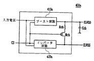
図3は、本発明に係るDC−DCコンバータの第1実施形態を示す構造図である。同図を参照して説明すると、DC−DCコンバータ400aは、ブースト回路410aと、インバータ回路420aと、キャパシタCchと、スイッチ部Rch、Mchとを含む。 FIG. 3 is a structural diagram showing a first embodiment of the DC-DC converter according to the present invention. Referring to the figure, the DC-DC converter 400a includes a boost circuit 410a, an inverter circuit 420a, a capacitor Cch, and switch units Rch and Mch.
ブースト回路410aは、入力電圧を受けて第1電圧ELVDDを生成する手段であって、入力電圧を昇圧して第1電圧ELVDDを生成する。入力電圧は、携帯電話のバッテリなどから伝達される。 The boost circuit 410a is a unit that receives the input voltage and generates the first voltage ELVDD, and boosts the input voltage to generate the first voltage ELVDD. The input voltage is transmitted from a cell phone battery or the like.
インバータ回路420aは、入力電圧を受けて第2電圧ELVSSを生成する手段であって、入力電圧を反転して低電圧を有する第2電圧ELVSSを生成する。 The inverter circuit 420a is a means for receiving the input voltage and generating the second voltage ELVSS, and inverts the input voltage to generate the second voltage ELVSS having a low voltage.
そして、ブースト回路410a及びインバータ回路420aは、制御信号CSを受信して動作の可否を決定する。 The boost circuit 410a and the inverter circuit 420a receive the control signal CS and determine whether or not to operate.
キャパシタCchは、DC−DCコンバータ400aの第1電圧ELVDDを出力する出力端に接続され、DC−DCコンバータ400aの出力を安定して出力できるようにする。 The capacitor Cch is connected to the output terminal for outputting the first voltage ELVDD of the DC-DC converter 400a, so that the output of the DC-DC converter 400a can be output stably.
スイッチ部Rch、Mchは、DC−DCコンバータ400aの内部に位置し、制御信号CSの動作に対応して、キャパシタCchに接続され、キャパシタCchに充電されている電荷を放電または保持させる。ブースト回路410aが駆動途中に制御信号CSによって停止すると、キャパシタCchには、第1電圧ELVDDの電荷が充電される。これにより、キャパシタCchに充電された電荷により、第1電圧ELVDDの電圧が図2に示されている画素部に伝達され、画素部のそれぞれの画素は、第1電圧ELVDDを受けて発光する。このような画素の発光は、ブースト回路410aの動作が停止した状態で発生するものであり、画素の寿命を短縮させる結果をもたらす。 The switch units Rch and Mch are located inside the DC-DC converter 400a, are connected to the capacitor Cch and discharge or hold the charge charged in the capacitor Cch in response to the operation of the control signal CS. When the boost circuit 410a is stopped by the control signal CS during driving, the capacitor Cch is charged with the first voltage ELVDD. Thereby, the voltage of the first voltage ELVDD is transmitted to the pixel portion shown in FIG. 2 by the electric charge charged in the capacitor Cch, and each pixel of the pixel portion receives the first voltage ELVDD and emits light. Such light emission of the pixel occurs when the operation of the boost circuit 410a is stopped, and results in shortening the lifetime of the pixel.
したがって、このような発光を防止するため、スイッチ部Rch、MchをキャパシタCchに接続し、キャパシタCchに格納された電荷を放電する経路を生成する。 Therefore, in order to prevent such light emission, the switch units Rch and Mch are connected to the capacitor Cch, and a path for discharging the charge stored in the capacitor Cch is generated.
スイッチ部Rch、Mchは、抵抗Rch及びトランジスタMchを含む。抵抗Rchは、一端がブースト回路410aの出力端に接続され、他端がトランジスタMchのソースに接続される。トランジスタMchは、ソースが抵抗Rchに接続され、ドレインがインバータ回路420aで生成された第2電圧ELVSSを出力する出力端に接続され、ゲートは、DC−DCコンバータ400aを動作させる制御信号CSを受信してスイッチング動作を行う。 The switch units Rch and Mch include a resistor Rch and a transistor Mch. The resistor Rch has one end connected to the output end of the boost circuit 410a and the other end connected to the source of the transistor Mch. The transistor Mch has a source connected to the resistor Rch, a drain connected to an output terminal that outputs the second voltage ELVSS generated by the inverter circuit 420a, and a gate that receives the control signal CS for operating the DC-DC converter 400a. Then, switching operation is performed.
すなわち、制御信号CSにより、DC−DCコンバータ400aが動作をすると、トランジスタMchはオフ状態になり、DC−DCコンバータ400aが動作を停止すると、トランジスタMchはオン状態になる。このため、トランジスタMchがオン状態になると、抵抗Rchの一端に第2電圧ELVSSが伝達され、キャパシタCchに格納された電荷が抵抗Rchを介して第2電圧ELVSSに流れ、キャパシタCchに格納された電荷が抵抗Rchで消費される。そして、トランジスタMchがオフ状態になると、抵抗Rchに電流が流れなくなり、ブースト回路410aの出力端の電圧への影響はない。 That is, when the DC-DC converter 400a operates according to the control signal CS, the transistor Mch is turned off, and when the DC-DC converter 400a stops operating, the transistor Mch is turned on. For this reason, when the transistor Mch is turned on, the second voltage ELVSS is transmitted to one end of the resistor Rch, and the charge stored in the capacitor Cch flows to the second voltage ELVSS via the resistor Rch and is stored in the capacitor Cch. Charge is consumed by the resistor Rch. When the transistor Mch is turned off, no current flows through the resistor Rch, and there is no effect on the voltage at the output terminal of the boost circuit 410a.
したがって、DC−DCコンバータ400aがオフ状態になったとき、キャパシタCchに充電された電荷が放電される。これにより、DC−DCコンバータ400aがオフ状態になっているとき、第1電圧ELVDDが、所定時間、図2の画素部に伝達されることを防止し、画素部のそれぞれの画素が異常発光する現象を防止することができる。 Therefore, when the DC-DC converter 400a is turned off, the charge charged in the capacitor Cch is discharged. Thus, when the DC-DC converter 400a is in the off state, the first voltage ELVDD is prevented from being transmitted to the pixel portion of FIG. 2 for a predetermined time, and each pixel of the pixel portion emits abnormal light. The phenomenon can be prevented.
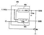
図4は、本発明に係るDC−DCコンバータの第2実施形態を示す構造図である。同図を参照して説明すると、DC−DCコンバータ400bは、ブースト回路410bと、インバータ回路420bと、キャパシタCchと、スイッチ部Rch、Mchとを含む。
FIG. 4 is a structural diagram showing a second embodiment of the DC-DC converter according to the present invention. Referring to the figure, the DC-
同図に示すDC−DCコンバータ400bは、図3に示すDC−DCコンバータ400aとは異なり、スイッチ部Rch、Mchにおいて、トランジスタMchの一端がインバータ回路420bの出力端に接続されるのではなく、アースに接続される。このため、制御信号CSに対応して、ブースト回路410bが停止した場合、キャパシタCchに格納された電荷がトランジスタMchを介してアースに流れる。
Unlike the DC-DC converter 400a shown in FIG. 3, in the DC-
したがって、DC−DCコンバータ400bがオフ状態になったとき、キャパシタCchに充電された電荷が放電される。これにより、DC−DCコンバータ400bがオフ状態になっているとき、第1電圧ELVDDが、所定時間、図2の画素部に伝達されることを防止し、画素部のそれぞれの画素が異常発光する現象を防止することができる。
Therefore, when the DC-
図5は、本発明に係るDC−DCコンバータの第3実施形態を示す構造図である。同図を参照して説明すると、DC−DCコンバータ400cは、ブースト回路410cと、インバータ回路420cとを含み、DC−DCコンバータ400cの出力端には、キャパシタCch及びスイッチ部Mchが接続される。
FIG. 5 is a structural diagram showing a third embodiment of the DC-DC converter according to the present invention. The DC-DC converter 400c includes a
図5に示すDC−DCコンバータ400cと、図3に示すDC−DCコンバータ400aとの相違点は、DC−DCコンバータ400cの外部にトランジスタMchが接続されることにある。 The difference between the DC-DC converter 400c shown in FIG. 5 and the DC-DC converter 400a shown in FIG. 3 is that a transistor Mch is connected to the outside of the DC-DC converter 400c.
トランジスタMchは、ソースが第1電圧ELVDDの出力端に接続され、ドレインがアースに接続される。このとき、インバータ回路420cの出力端は、アースに接続されない。これにより、制御信号CSに対応して、ブースト回路410cが停止した場合、キャパシタCchに格納された電荷がトランジスタMchを介してアースに流れる。
The transistor Mch has a source connected to the output terminal of the first voltage ELVDD and a drain connected to the ground. At this time, the output terminal of the
したがって、DC−DCコンバータ400cがオフ状態になったとき、キャパシタCchに充電された電荷が放電される。これにより、DC−DCコンバータ400cがオフ状態になっているとき、第1電圧ELVDDが、所定時間、図2の画素部に伝達されることを防止し、画素部のそれぞれの画素が異常発光する現象を防止することができる。 Therefore, when the DC-DC converter 400c is turned off, the charge charged in the capacitor Cch is discharged. Accordingly, when the DC-DC converter 400c is in an off state, the first voltage ELVDD is prevented from being transmitted to the pixel portion of FIG. 2 for a predetermined time, and each pixel of the pixel portion emits abnormal light. The phenomenon can be prevented.
図6は、本発明に係るDC−DCコンバータの第4実施形態を示す構造図である。同図を参照して説明すると、DC−DCコンバータ400dは、ブースト回路410dと、インバータ回路420dとを含み、DC−DCコンバータ400dの出力端には、キャパシタCch及びスイッチ部が接続され、制御信号CSの入力端とスイッチ部との間には、遅延回路430が接続される。
FIG. 6 is a structural diagram showing a fourth embodiment of the DC-DC converter according to the present invention. The DC-
ブースト回路410dは、入力電圧を受けて第1電圧ELVDDを生成する手段であって、入力電圧を昇圧して第1電圧ELVDDを生成する。入力電圧は、携帯電話のバッテリなどから伝達される。
The
インバータ回路420dは、入力電圧を受けて第2電圧ELVSSを生成する手段であって、入力電圧を反転して低電圧を有する第2電圧ELVSSを生成する。 The inverter circuit 420d is a unit that receives the input voltage and generates the second voltage ELVSS, and inverts the input voltage to generate the second voltage ELVSS having a low voltage.
そして、ブースト回路410d及びインバータ回路420dは、制御信号CSを受信して動作の可否を決定する。
The
キャパシタCchは、DC−DCコンバータ400dの出力端に接続され、DC−DCコンバータ400dの出力を安定して出力できるようにする。
The capacitor Cch is connected to the output terminal of the DC-
スイッチ部は、DC−DCコンバータ400dの外部に形成され、キャパシタCchに充電されている電荷を放電させる。キャパシタCchに充電された電荷が放電されない状態で、DC−DCコンバータ400dが動作途中に停止すると、キャパシタCchには、第1電圧ELVDDの電荷が充電されるようになる。キャパシタCchに充電された電荷により、第1電圧ELVDDの電荷が、インバータ回路420dを介して、図2に示されている画素部に伝達され、画素部のそれぞれの画素は、第1電圧ELVDDを受けて発光する。このような画素の発光は、DC−DCコンバータ400dの動作が停止した状態で発生するものであり、画素の寿命が短縮する結果をもたらす。したがって、このような発光を防止するため、スイッチ部において、キャパシタCchに格納された電荷を放電する経路を生成する。スイッチ部は、トランジスタMchを含み、トランジスタMchは、ソースがブースト回路410dの出力端に接続され、ドレインがアースに接続され、ゲートは、DC−DCコンバータ400dを動作させる制御信号CSを受信してスイッチング動作を行う。すなわち、制御信号CSにより、DC−DCコンバータ400dが動作をすると、トランジスタMchはオフ状態になり、DC−DCコンバータ400dが動作を停止すると、トランジスタMchはオン状態になる。このため、トランジスタMchがオン状態になると、キャパシタCchに格納されている電荷がトランジスタMchを介してアースに流れ、キャパシタCchに格納された電荷が放電される。そして、トランジスタMchがオフ状態になると、アースに電流が流れなくなり、ブースト回路410dの出力端の電圧への影響はない。
The switch unit is formed outside the DC-
すなわち、DC−DCコンバータ400dがオフ状態になったとき、キャパシタCchに充電された電荷が放電される。これにより、DC−DCコンバータ400cがオフ状態になっているとき、第1電圧ELVDDが、所定時間、図2の画素部に伝達されることを防止し、画素部のそれぞれの画素が異常発光する現象を防止することができる。
That is, when the DC-
遅延回路430は、DC−DCコンバータ400dの駆動を決定する制御信号CSを一定時間の経過後にトランジスタMchに伝達させる手段である。このような遅延回路430は、DC−DCコンバータ400dが停止した後、所定時間の経過後に、トランジスタMchがオン状態になるようにし、キャパシタCchに格納された電荷がトランジスタMchを介してアースに流れるようにする。このため、DC−DCコンバータ400dの制御信号CSによる駆動停止後、キャパシタCchに充電された電荷は、直ちにトランジスタMchを介してアースに流れるのではなく、時間差をおいて、トランジスタMchを介してアースに流れ、第1電圧ELVDDが直ちに遮断されないようにする。
The
図7は、本発明に係るDC−DCコンバータの第5実施形態を示す構造図である。同図を参照して説明すると、DC−DCコンバータ400eは、ブースト回路410eと、インバータ回路420eとを含み、DC−DCコンバータ400eの出力端には、キャパシタCch及び抵抗Rchが接続される。
FIG. 7 is a structural diagram showing a fifth embodiment of the DC-DC converter according to the present invention. The DC-
ブースト回路410eは、入力電圧を受けて第1電圧ELVDDを生成する手段であって、入力電圧を昇圧して第1電圧ELVDDを生成する。入力電圧は、携帯電話のバッテリなどから伝達される。 The boost circuit 410e is means for receiving the input voltage and generating the first voltage ELVDD, and boosts the input voltage to generate the first voltage ELVDD. The input voltage is transmitted from a cell phone battery or the like.
インバータ回路420eは、入力電圧を受けて第2電圧ELVSSを生成する手段であって、入力電圧を反転して低電圧を有する第2電圧ELVSSを生成する。
The
そして、ブースト回路410e及びインバータ回路420eは、制御信号CSを受信して動作の可否を決定する。
Then, the boost circuit 410e and the
キャパシタCchは、DC−DCコンバータ400eの出力端に接続され、DC−DCコンバータ400eの出力を安定して出力できるようにする。
The capacitor Cch is connected to the output terminal of the DC-
抵抗Rchは、DC−DCコンバータ400eの外部に形成され、キャパシタCchに充電されている電荷を放電させる。キャパシタCchに充電された電荷を放電させなくなると、DC−DCコンバータ400eが動作途中に動作を停止し、キャパシタCchには、第1電圧ELVDDの電荷が充電されるようになる。キャパシタCchに充電された電荷により、第1電圧ELVDDの電荷が、ブースト回路410eを介して、図2に示されている画素部に伝達され、画素部のそれぞれの画素は、第1電圧ELVDDを受けて発光する。このような画素の発光は、DC−DCコンバータ400eが動作を停止した状態で発生するものであり、画素の寿命などに悪い影響を及ぼす。したがって、このような発光を防止するため、抵抗Rchを介してキャパシタCchに格納された電荷を放電する経路を生成する。抵抗Rchの一端は、DC−DCコンバータ400eの出力端に接続され、他端は、アースに接続される。このため、キャパシタCchに充電された電荷が抵抗Rchを介して消費される。キャパシタCchに充電された電荷が放電する時間は、キャパシタCchの大きさ及び抵抗Rchの大きさに対応するため、キャパシタCch及び抵抗Rchの大きさを調整し、キャパシタCchに充電された電荷が非常に早く消費されることを防止する。
The resistor Rch is formed outside the DC-
したがって、DC−DCコンバータ400eの出力端に格納されている電荷が放電され、DC−DCコンバータ400eがオフ状態になった後、第1電圧ELVDDの電圧が、図2の画素部に伝達されることを防止し、画素部のそれぞれの画素が異常発光する現象を防止することができる。
Therefore, after the charge stored at the output terminal of the DC-
図8は、本発明に係るDC−DCコンバータの第6実施形態を示す構造図である。同図を参照して説明すると、DC−DCコンバータ400fは、ブースト回路410fと、インバータ回路420fとを含み、DC−DCコンバータ400fの出力端には、キャパシタCch1、Cch2及び抵抗Rchが接続される。 FIG. 8 is a structural diagram showing a sixth embodiment of the DC-DC converter according to the present invention. The DC-DC converter 400f includes a boost circuit 410f and an inverter circuit 420f. Capacitors Cch1, Cch2 and a resistor Rch are connected to the output terminal of the DC-DC converter 400f. .
ブースト回路410fは、入力電圧を受けて第1電圧ELVDDを生成する手段であって、入力電圧を昇圧して第1電圧ELVDDを生成する。入力電圧は、携帯電話のバッテリなどから伝達される。 The boost circuit 410f is means for receiving the input voltage and generating the first voltage ELVDD, and boosts the input voltage to generate the first voltage ELVDD. The input voltage is transmitted from a cell phone battery or the like.
インバータ回路420fは、入力電圧を受けて第2電圧ELVSSを生成する手段であって、入力電圧を反転して低電圧を有する第2電圧ELVSSを生成する。 The inverter circuit 420f is a unit that receives the input voltage and generates the second voltage ELVSS, and inverts the input voltage to generate the second voltage ELVSS having a low voltage.
そして、ブースト回路410f及びインバータ回路420fは、制御信号CSを受信して動作の可否を決定する。 The boost circuit 410f and the inverter circuit 420f receive the control signal CS and determine whether or not to operate.
キャパシタCch1、Cch2は、ブースト回路410f及びインバータ回路420fの出力端にそれぞれ接続され、第1電圧ELVDDの電圧及び第2電圧ELVSSの電圧を安定して出力できるようにする。 The capacitors Cch1 and Cch2 are connected to the output terminals of the boost circuit 410f and the inverter circuit 420f, respectively, and can stably output the voltage of the first voltage ELVDD and the voltage of the second voltage ELVSS.
抵抗Rchは、DC−DCコンバータ400fの外部に形成され、キャパシタCch1、Cch2に充電されている電荷を放電させる。キャパシタCch1、Cch2に充電された電荷を放電させなくなると、DC−DCコンバータ400fが動作途中に動作を停止し、キャパシタCch1、Cch2には、第1電圧ELVDDの電荷が充電される。キャパシタCch1、Cch2に充電された電荷により、第1電圧ELVDDの電圧が、ブースト回路410fを介して、図2に示されている画素部に伝達され、画素部のそれぞれの画素は、第1電圧ELVDDを受けて発光する。このような画素の発光は、DC−DCコンバータ400fが動作を停止した状態で発生するものであり、画素の寿命などに悪い影響を及ぼす。したがって、このような発光を防止するため、抵抗Rchを介してキャパシタCch1、Cch2に格納された電荷を放電する経路を生成する。抵抗Rchの一端は、ブースト回路410fの出力端に接続され、他端は、インバータ回路420fの出力端に接続される。このため、抵抗Rchが第1電圧ELVDDの電圧と第2電圧ELVSSの電圧との間に位置し、キャパシタCch1、Cch2に充電された電荷が抵抗Rchを介して消費される。キャパシタCch1、Cch2に充電された電荷が放電する時間は、キャパシタCch1、Cch2の大きさ及び抵抗Rchの大きさに対応するため、キャパシタCch1、Cch2及び抵抗Rchの大きさを調整し、キャパシタCch1、Cch2に充電された電荷が非常に早く消費されることを防止する。 The resistor Rch is formed outside the DC-DC converter 400f and discharges the charges charged in the capacitors Cch1 and Cch2. When the charges charged in the capacitors Cch1 and Cch2 are not discharged, the DC-DC converter 400f stops operating during the operation, and the capacitors Cch1 and Cch2 are charged with the charge of the first voltage ELVDD. Due to the electric charges charged in the capacitors Cch1 and Cch2, the voltage of the first voltage ELVDD is transmitted to the pixel portion shown in FIG. 2 via the boost circuit 410f, and each pixel of the pixel portion receives the first voltage. Lights upon receiving ELVDD. Such light emission of the pixel occurs when the DC-DC converter 400f stops its operation, and adversely affects the lifetime of the pixel. Therefore, in order to prevent such light emission, a path for discharging the charges stored in the capacitors Cch1 and Cch2 through the resistor Rch is generated. One end of the resistor Rch is connected to the output end of the boost circuit 410f, and the other end is connected to the output end of the inverter circuit 420f. For this reason, the resistor Rch is positioned between the voltage of the first voltage ELVDD and the voltage of the second voltage ELVSS, and the charges charged in the capacitors Cch1 and Cch2 are consumed via the resistor Rch. The time for which the charges charged in the capacitors Cch1 and Cch2 are discharged corresponds to the size of the capacitors Cch1 and Cch2 and the size of the resistor Rch. Therefore, the sizes of the capacitors Cch1, Cch2 and the resistor Rch are adjusted, and the capacitors Cch1, The electric charge charged in Cch2 is prevented from being consumed very quickly.
したがって、DC−DCコンバータ400fの出力端に格納されている電荷が放電され、DC−DCコンバータ400fの出力端に格納されていた電荷が、DC−DCコンバータ400fがオフ状態になった後、図2の画素部に伝達されることを防止し、画素部のそれぞれの画素が異常発光する現象を防止することができる。 Therefore, after the electric charge stored at the output terminal of the DC-DC converter 400f is discharged and the electric charge stored at the output terminal of the DC-DC converter 400f is turned off, the DC-DC converter 400f is turned off. It is possible to prevent the light from being transmitted to the two pixel portions, and to prevent a phenomenon in which each pixel in the pixel portion emits abnormal light.
100 画素部
101 画素
200 データ駆動部
300 走査駆動部
400 DC−DCコンバータ
410a、410b、410c、410d、410e、410f ブースト回路
420a、420b、420c、420d、420e、420f インバータ回路
430 遅延回路
100 pixel unit 101
Claims (15)
前記第1出力端に接続されるキャパシタと、
前記制御信号により、前記キャパシタに格納された電荷を放電するスイッチ部と、を含み、
前記電圧生成部が制御信号により動作をする場合に前記スイッチはオフ状態になり、前記電圧生成部が制御信号により動作を停止する場合に前記スイッチはオン状態になって前記キャパシタの電荷を放電させる
ことを特徴とするDC−DCコンバータ。 A first voltage and a second voltage lower than the first voltage are generated from an input voltage received via an input terminal, the generated first voltage is output from a first output terminal, and the generated second voltage is A voltage generation unit that outputs from the second output terminal, receives a control signal, and determines whether or not the operation is possible;
A capacitor connected to the first output terminal ;
By the control signal, seen including and a switch unit for discharging the stored charge in the capacitor,
The switch is turned off when the voltage generator operates according to the control signal, and the switch is turned on when the voltage generator stops operation according to the control signal, and discharges the capacitor charge. The DC-DC converter characterized by the above-mentioned.
前記第1電圧を生成するブースト回路と、
前記第2電圧を生成するインバータ回路と、をさらに含む
ことを特徴とする請求項1に記載のDC−DCコンバータ。 The voltage generator is
A boost circuit for generating the first voltage;
The DC-DC converter according to claim 1, further comprising: an inverter circuit that generates the second voltage.
ことを特徴とする請求項1に記載のDC−DCコンバータ。 The DC-DC converter according to claim 1, wherein the switch unit further includes a transistor whose on / off state is determined by the control signal.
ことを特徴とする請求項3に記載のDC−DCコンバータ。 The DC-DC converter according to claim 3, further comprising a resistor that discharges the electric charge charged in the capacitor and is connected by the transistor.
ことを特徴とする請求項3に記載のDC−DCコンバータ。 The DC-DC converter according to claim 3, further comprising a delay circuit that receives the control signal and transmits the control signal to the gate of the transistor with a predetermined time delay .
ことを特徴とする請求項3に記載のDC−DCコンバータ。 The DC-DC converter according to claim 3, wherein the transistor is connected to ground.
ことを特徴とする請求項3に記載のDC−DCコンバータ。 The DC-DC converter according to claim 3, wherein the transistor is connected to the second voltage.
前記第1出力端に接続されるキャパシタと、
前記出力端、前記第2電圧、及びアースのいずれか1つに接続され、前記キャパシタに格納されている電荷を消耗する抵抗と、を含み、
前記電圧生成部が制御信号により動作をする場合に前記スイッチはオフ状態になり、前記電圧生成部が制御信号により動作を停止する場合に前記スイッチはオン状態になって前記キャパシタの電荷を放電させる
ことを特徴とするDC−DCコンバータ。 A first voltage and a second voltage lower than the first voltage are generated from an input voltage received via an input terminal, the generated first voltage is output from a first output terminal, and the generated second voltage is A voltage generation unit that outputs from the second output terminal, receives a control signal, and determines whether or not the operation is possible;
A capacitor connected to the first output terminal ;
Said output terminal, said second voltage, and is connected to one ground, seen including a resistor, a to consume charge stored in the capacitor,
The switch is turned off when the voltage generator operates according to the control signal, and the switch is turned on when the voltage generator stops operation according to the control signal, and discharges the capacitor charge. The DC-DC converter characterized by the above-mentioned.
前記データ信号を生成するデータ駆動部と、
前記走査信号を生成する走査駆動部と、
前記第1電圧及び前記第2電圧を生成するDC−DCコンバータと、を備え、
前記DC−DCコンバータは、
入力端を介して受けた入力電圧から前記第1電圧と前記第1電圧より低い前記第2電圧とを生成し、生成した前記第1電圧を第1出力端から出力し、生成した前記第2電圧を第2出力端から出力すると共に、制御信号を受信して動作の可否が決定される電圧生成部と、
前記第1出力端に接続されるキャパシタと、
前記制御信号により、前記キャパシタに格納された電荷を放電するスイッチ部と、を含み、
前記電圧生成部が制御信号により動作をする場合に前記スイッチはオフ状態になり、前記電圧生成部が制御信号により動作を停止する場合に前記スイッチはオン状態になって前記キャパシタの電荷を放電させる
ことを特徴とする有機電界発光表示装置。 A pixel unit that receives the data signal, the scanning signal, the first voltage, and the second voltage to express an image;
A data driver for generating the data signal;
A scan driver for generating the scan signal;
A DC-DC converter that generates the first voltage and the second voltage,
The DC-DC converter
The first voltage and the second voltage lower than the first voltage are generated from the input voltage received through the input terminal, the generated first voltage is output from the first output terminal, and the generated second voltage is generated. A voltage generating unit that outputs a voltage from the second output terminal and receives a control signal to determine whether or not to operate;
A capacitor connected to the first output terminal ;
By the control signal, seen including and a switch unit for discharging the stored charge in the capacitor,
The switch is turned off when the voltage generator operates according to the control signal, and the switch is turned on when the voltage generator stops operation according to the control signal, and discharges the capacitor charge. An organic electroluminescent display device characterized by the above.
前記第1電圧を生成するブースト回路と、
前記第2電圧を生成するインバータ回路と、をさらに含む
ことを特徴とする請求項9に記載の有機電界表示装置。 The voltage generator is
A boost circuit for generating the first voltage;
The organic electric field display device according to claim 9, further comprising: an inverter circuit that generates the second voltage.
ことを特徴とする請求項9に記載の有機電界表示装置。 The organic electric field display device according to claim 9, wherein the switch unit further includes a transistor whose ON / OFF state is determined by the control signal.
ことを特徴とする請求項11に記載の有機電界表示装置。 The organic electric field display device according to claim 11, further comprising a delay circuit that receives the control signal and transmits the control signal to the gate of the transistor with a certain delay .
ことを特徴とする請求項11に記載の有機電界表示装置。 The organic electric field display device according to claim 11, wherein the transistor is connected to a ground.
ことを特徴とする請求項11に記載の有機電界表示装置。 The organic electric field display device according to claim 11, wherein the transistor is connected to the second voltage.
前記データ信号を生成するデータ駆動部と、
前記走査信号を生成する走査駆動部と、
前記第1電圧及び前記第2電圧を生成するDC−DCコンバータと、を備え、
前記DC−DCコンバータは、
入力端を介して受けた入力電圧から前記第1電圧と前記第1電圧より低い前記第2電圧とを生成し、生成した前記第1電圧を第1出力端から出力し、生成した前記第2電圧を第2出力端から出力すると共に、制御信号を受信して動作の可否が決定される電圧生成部と、
前記第1出力端に接続されるキャパシタ
前記出力端と前記第2電圧またはアースとの間に接続され、前記キャパシタに格納されている電荷を消耗する抵抗と、を含み、
前記電圧生成部が制御信号により動作をする場合に前記キャパシタが充電され、前記電圧生成部が制御信号により動作を停止する場合に前記抵抗を介して前記キャパシタの電荷を放電させる
ことを特徴とする有機電界発光表示装置。 A pixel unit that receives the data signal, the scanning signal, the first voltage, and the second voltage to express an image;
A data driver for generating the data signal;
A scan driver for generating the scan signal;
A DC-DC converter that generates the first voltage and the second voltage,
The DC-DC converter
The first voltage and the second voltage lower than the first voltage are generated from the input voltage received through the input terminal, the generated first voltage is output from the first output terminal, and the generated second voltage is generated. A voltage generating unit that outputs a voltage from the second output terminal, receives a control signal, and determines whether the operation is possible;
Connected between the said capacitor and the output terminal connected to the first output terminal the second voltage or ground, seen including a resistor, a to consume charge stored in the capacitor,
The capacitor is charged when the voltage generator is operated by a control signal, and the capacitor is discharged through the resistor when the voltage generator is stopped by a control signal. Organic electroluminescent display device.
Applications Claiming Priority (1)
| Application Number | Priority Date | Filing Date | Title |
|---|---|---|---|
| KR1020070086511A KR100889690B1 (en) | 2007-08-28 | 2007-08-28 | Converter and organic light emitting display thereof |
Publications (2)
| Publication Number | Publication Date |
|---|---|
| JP2009055774A JP2009055774A (en) | 2009-03-12 |
| JP4659807B2 true JP4659807B2 (en) | 2011-03-30 |
Family
ID=40092049
Family Applications (1)
| Application Number | Title | Priority Date | Filing Date |
|---|---|---|---|
| JP2007275362A Active JP4659807B2 (en) | 2007-08-28 | 2007-10-23 | DC-DC converter and organic light emitting display using the same |
Country Status (5)
| Country | Link |
|---|---|
| US (1) | US8749462B2 (en) |
| EP (1) | EP2031941A3 (en) |
| JP (1) | JP4659807B2 (en) |
| KR (1) | KR100889690B1 (en) |
| CN (1) | CN101378229A (en) |
Families Citing this family (23)
| Publication number | Priority date | Publication date | Assignee | Title |
|---|---|---|---|---|
| JP4502003B2 (en) * | 2007-12-26 | 2010-07-14 | エプソンイメージングデバイス株式会社 | Electro-optical device and electronic apparatus including the electro-optical device |
| KR100952834B1 (en) * | 2008-08-06 | 2010-04-15 | 삼성모바일디스플레이주식회사 | Dc-dc converter and organic light emitting display using the same |
| JP5515331B2 (en) | 2009-03-09 | 2014-06-11 | ソニー株式会社 | Information providing server, information providing system, information providing method, and program |
| KR101049019B1 (en) * | 2009-05-19 | 2011-07-12 | 삼성모바일디스플레이주식회사 | Power supply unit and organic light emitting display device using the same |
| KR101067225B1 (en) * | 2009-07-08 | 2011-09-22 | 삼성전기주식회사 | On/Off Sequence Circuit for Using Plasma Display Panel |
| KR101022085B1 (en) * | 2009-07-10 | 2011-03-17 | 삼성모바일디스플레이주식회사 | Power supply and organic light emitting display device using the same |
| KR101084170B1 (en) * | 2009-08-03 | 2011-11-17 | 삼성모바일디스플레이주식회사 | Power control system for display module with external DC-DC convertor |
| KR101064462B1 (en) * | 2009-11-17 | 2011-09-15 | 삼성모바일디스플레이주식회사 | Dc-dc converter and organic light emitting display device for the same |
| KR101040798B1 (en) * | 2009-11-17 | 2011-06-14 | 삼성모바일디스플레이주식회사 | Dc-dc conveter and organic light emitting display device using the same |
| KR101132023B1 (en) | 2010-02-19 | 2012-04-02 | 삼성모바일디스플레이주식회사 | Dc-dc converter and organic light emitting display using the same |
| KR101887336B1 (en) * | 2010-04-23 | 2018-08-09 | 가부시키가이샤 한도오따이 에네루기 켄큐쇼 | Display device and driving method thereof |
| KR101193194B1 (en) * | 2010-04-30 | 2012-10-19 | 삼성디스플레이 주식회사 | Organic Light Emitting Display |
| KR101992281B1 (en) * | 2012-03-06 | 2019-06-26 | 삼성디스플레이 주식회사 | Organic Light Emitting Display and Driving Method Thereof |
| KR101975531B1 (en) * | 2012-09-10 | 2019-05-08 | 삼성디스플레이 주식회사 | Organic Light Emitting Display Device and Driving Method Thereof |
| KR102071004B1 (en) | 2013-09-03 | 2020-01-30 | 삼성디스플레이 주식회사 | Dc-dc converter and organic light emitting display including the same |
| KR102141207B1 (en) * | 2013-11-11 | 2020-08-05 | 삼성디스플레이 주식회사 | Display apparatus, power voltage generating apparatus, and method for generating power voltage |
| KR102395148B1 (en) | 2015-03-03 | 2022-05-09 | 삼성디스플레이 주식회사 | Dc-dc converter and display device having the same |
| KR102484869B1 (en) * | 2015-12-02 | 2023-01-06 | 엘지디스플레이 주식회사 | Organic light emitting display device and method for driving organic light emitting display device |
| KR102430795B1 (en) * | 2015-12-31 | 2022-08-08 | 엘지디스플레이 주식회사 | Display device and method for driving the same |
| CN105657898B (en) * | 2016-02-19 | 2017-12-08 | 京东方科技集团股份有限公司 | A kind of power circuit and its driving method, display device |
| CN107103871B (en) * | 2017-06-30 | 2019-11-22 | 京东方科技集团股份有限公司 | The power supply circuit and method of supplying power to of display device and display screen |
| CN110544452B (en) * | 2018-05-28 | 2021-08-17 | 京东方科技集团股份有限公司 | Power supply time sequence control circuit and control method, display driving circuit and display device |
| KR102519570B1 (en) | 2018-11-12 | 2023-04-10 | 삼성디스플레이 주식회사 | Display apparatus and method of driving display panel using the same |
Citations (3)
| Publication number | Priority date | Publication date | Assignee | Title |
|---|---|---|---|---|
| JPH05236744A (en) * | 1992-02-19 | 1993-09-10 | Ricoh Co Ltd | Multioutput swtching power source unit |
| JP2005315919A (en) * | 2004-04-27 | 2005-11-10 | Tohoku Pioneer Corp | Light-emitting display apparatus and control method for driving the same |
| JP2006189714A (en) * | 2005-01-07 | 2006-07-20 | Casio Comput Co Ltd | Display driving device and display apparatus, and its driving control method |
Family Cites Families (20)
| Publication number | Priority date | Publication date | Assignee | Title |
|---|---|---|---|---|
| US4422073A (en) * | 1981-10-27 | 1983-12-20 | The Bendix Corporation | Combustible gas detection system |
| CN1023048C (en) | 1989-08-17 | 1993-12-08 | 哈尔滨工业大学 | Phase cut-off protector of phase and width discrimination |
| JP2000152623A (en) | 1998-11-10 | 2000-05-30 | Ricoh Co Ltd | Power unit |
| GB9921425D0 (en) | 1999-09-11 | 1999-11-10 | Koninkl Philips Electronics Nv | Active matrix electroluminescent display device |
| KR100389019B1 (en) * | 2000-11-22 | 2003-06-25 | 엘지전자 주식회사 | Reset Circuit in Plasma Display Panel |
| JP2002233139A (en) | 2001-02-05 | 2002-08-16 | Matsushita Electric Ind Co Ltd | Dc-dc converter |
| JP2002244617A (en) * | 2001-02-15 | 2002-08-30 | Sanyo Electric Co Ltd | Organic el pixel circuit |
| JP3788916B2 (en) | 2001-03-30 | 2006-06-21 | 株式会社日立製作所 | Light-emitting display device |
| KR100878222B1 (en) | 2001-07-03 | 2009-01-13 | 삼성전자주식회사 | Apparatus for supplying power for a liquid crystal display |
| US7483001B2 (en) | 2001-11-21 | 2009-01-27 | Seiko Epson Corporation | Active matrix substrate, electro-optical device, and electronic device |
| US7698573B2 (en) * | 2002-04-02 | 2010-04-13 | Sharp Corporation | Power source apparatus for display and image display apparatus |
| KR100514185B1 (en) * | 2003-10-01 | 2005-09-13 | 삼성에스디아이 주식회사 | DC-DC Converter for electro luminescence display |
| US6913554B2 (en) * | 2003-10-03 | 2005-07-05 | Gilbert W. Younger | Methods and systems for improving the operation of transmissions for motor vehicles |
| KR20050046927A (en) * | 2003-11-14 | 2005-05-19 | 삼성에스디아이 주식회사 | Power supply and light emitting display device using the power supply |
| GB0400213D0 (en) | 2004-01-07 | 2004-02-11 | Koninkl Philips Electronics Nv | Electroluminescent display devices |
| KR100662981B1 (en) * | 2004-11-04 | 2006-12-28 | 삼성에스디아이 주식회사 | Light emitting display and DC-DC converter thereof |
| CN100486089C (en) | 2004-12-25 | 2009-05-06 | 鸿富锦精密工业(深圳)有限公司 | Switching power supply |
| KR100649508B1 (en) * | 2005-02-02 | 2006-11-27 | 권오영 | Hybrid power supply system |
| KR101152118B1 (en) | 2005-02-16 | 2012-06-15 | 삼성전자주식회사 | Driving apparatus of display device and dc-dc converter |
| KR20080064564A (en) * | 2007-01-05 | 2008-07-09 | 삼성전자주식회사 | Printed circuit board and liquid crystal display device having the same |
-
2007
- 2007-08-28 KR KR1020070086511A patent/KR100889690B1/en active IP Right Grant
- 2007-10-23 JP JP2007275362A patent/JP4659807B2/en active Active
-
2008
- 2008-07-08 US US12/217,817 patent/US8749462B2/en active Active
- 2008-08-26 CN CNA2008102124427A patent/CN101378229A/en active Pending
- 2008-08-27 EP EP08163107A patent/EP2031941A3/en not_active Withdrawn
Patent Citations (3)
| Publication number | Priority date | Publication date | Assignee | Title |
|---|---|---|---|---|
| JPH05236744A (en) * | 1992-02-19 | 1993-09-10 | Ricoh Co Ltd | Multioutput swtching power source unit |
| JP2005315919A (en) * | 2004-04-27 | 2005-11-10 | Tohoku Pioneer Corp | Light-emitting display apparatus and control method for driving the same |
| JP2006189714A (en) * | 2005-01-07 | 2006-07-20 | Casio Comput Co Ltd | Display driving device and display apparatus, and its driving control method |
Also Published As
| Publication number | Publication date |
|---|---|
| US20090058311A1 (en) | 2009-03-05 |
| KR20090021742A (en) | 2009-03-04 |
| EP2031941A2 (en) | 2009-03-04 |
| KR100889690B1 (en) | 2009-03-19 |
| US8749462B2 (en) | 2014-06-10 |
| EP2031941A3 (en) | 2012-01-11 |
| CN101378229A (en) | 2009-03-04 |
| JP2009055774A (en) | 2009-03-12 |
Similar Documents
| Publication | Publication Date | Title |
|---|---|---|
| JP4659807B2 (en) | DC-DC converter and organic light emitting display using the same | |
| KR101064462B1 (en) | Dc-dc converter and organic light emitting display device for the same | |
| JP4981099B2 (en) | DC-DC converter and organic light emitting display using the same | |
| TWI547924B (en) | Organic light emitting display and driving method thereof | |
| KR101829398B1 (en) | Organic Light Emitting Display and Driving Method Thereof | |
| US9064456B2 (en) | Organic light emitting diode display having short detecting circuit and method of driving the same | |
| US8791886B2 (en) | DC-DC converter and organic light emitting display device including the same | |
| KR101146989B1 (en) | DC-DC converter, Organic electro luminescence Display having the same and driving method thereof | |
| TWI604425B (en) | Organic light emitting display | |
| US20130229402A1 (en) | Power generator and organic light emitting display device using the same | |
| US10170047B2 (en) | Organic light emitting display and driving method thereof | |
| JP2010041909A (en) | Dc-dc converter, and organic electric field light-emitting display unit using the same | |
| KR101040798B1 (en) | Dc-dc conveter and organic light emitting display device using the same | |
| KR20130003246A (en) | Dc-dc converter and organic light emitting display including the same | |
| KR20110013687A (en) | Organic lighting emitting display device and driving method using the same | |
| JP2009139935A (en) | Organic electroluminescent display device and driving method thereof | |
| US9207785B2 (en) | Voltage generator and organic light emitting display device using the same | |
| US20100220088A1 (en) | Power supply unit and organic light emitting display device using the same | |
| CN100428312C (en) | Electrolumi nescence display device and its driving method | |
| US8373689B2 (en) | Organic light emitting diode display device | |
| KR20090093019A (en) | Dc-dc converter and organic light emitting display thereof |
Legal Events
| Date | Code | Title | Description |
|---|---|---|---|
| A711 | Notification of change in applicant |
Free format text: JAPANESE INTERMEDIATE CODE: A712 Effective date: 20081208 |
|
| A521 | Request for written amendment filed |
Free format text: JAPANESE INTERMEDIATE CODE: A523 Effective date: 20090225 |
|
| A131 | Notification of reasons for refusal |
Free format text: JAPANESE INTERMEDIATE CODE: A131 Effective date: 20100817 |
|
| A521 | Request for written amendment filed |
Free format text: JAPANESE INTERMEDIATE CODE: A523 Effective date: 20101116 |
|
| TRDD | Decision of grant or rejection written | ||
| A01 | Written decision to grant a patent or to grant a registration (utility model) |
Free format text: JAPANESE INTERMEDIATE CODE: A01 Effective date: 20101207 |
|
| A01 | Written decision to grant a patent or to grant a registration (utility model) |
Free format text: JAPANESE INTERMEDIATE CODE: A01 |
|
| A61 | First payment of annual fees (during grant procedure) |
Free format text: JAPANESE INTERMEDIATE CODE: A61 Effective date: 20101227 |
|
| FPAY | Renewal fee payment (event date is renewal date of database) |
Free format text: PAYMENT UNTIL: 20140107 Year of fee payment: 3 |
|
| R150 | Certificate of patent or registration of utility model |
Ref document number: 4659807 Country of ref document: JP Free format text: JAPANESE INTERMEDIATE CODE: R150 |
|
| FPAY | Renewal fee payment (event date is renewal date of database) |
Free format text: PAYMENT UNTIL: 20140107 Year of fee payment: 3 |
|
| S111 | Request for change of ownership or part of ownership |
Free format text: JAPANESE INTERMEDIATE CODE: R313111 |
|
| FPAY | Renewal fee payment (event date is renewal date of database) |
Free format text: PAYMENT UNTIL: 20140107 Year of fee payment: 3 |
|
| R350 | Written notification of registration of transfer |
Free format text: JAPANESE INTERMEDIATE CODE: R350 |
|
| R250 | Receipt of annual fees |
Free format text: JAPANESE INTERMEDIATE CODE: R250 |
|
| R250 | Receipt of annual fees |
Free format text: JAPANESE INTERMEDIATE CODE: R250 |
|
| R250 | Receipt of annual fees |
Free format text: JAPANESE INTERMEDIATE CODE: R250 |
|
| R250 | Receipt of annual fees |
Free format text: JAPANESE INTERMEDIATE CODE: R250 |
|
| R250 | Receipt of annual fees |
Free format text: JAPANESE INTERMEDIATE CODE: R250 |
|
| R250 | Receipt of annual fees |
Free format text: JAPANESE INTERMEDIATE CODE: R250 |
|
| R250 | Receipt of annual fees |
Free format text: JAPANESE INTERMEDIATE CODE: R250 |
|
| R250 | Receipt of annual fees |
Free format text: JAPANESE INTERMEDIATE CODE: R250 |
|
| R250 | Receipt of annual fees |
Free format text: JAPANESE INTERMEDIATE CODE: R250 |
|
| R250 | Receipt of annual fees |
Free format text: JAPANESE INTERMEDIATE CODE: R250 |
|
| R250 | Receipt of annual fees |
Free format text: JAPANESE INTERMEDIATE CODE: R250 |