EP2031941A2 - DC-DC converter and organic light emitting display using the same - Google Patents
DC-DC converter and organic light emitting display using the same Download PDFInfo
- Publication number
- EP2031941A2 EP2031941A2 EP08163107A EP08163107A EP2031941A2 EP 2031941 A2 EP2031941 A2 EP 2031941A2 EP 08163107 A EP08163107 A EP 08163107A EP 08163107 A EP08163107 A EP 08163107A EP 2031941 A2 EP2031941 A2 EP 2031941A2
- Authority
- EP
- European Patent Office
- Prior art keywords
- converter
- voltage
- capacitor
- coupled
- generate
- Prior art date
- Legal status (The legal status is an assumption and is not a legal conclusion. Google has not performed a legal analysis and makes no representation as to the accuracy of the status listed.)
- Withdrawn
Links
- 239000003990 capacitor Substances 0.000 claims abstract description 71
- 238000007599 discharging Methods 0.000 abstract description 8
- 238000004020 luminiscence type Methods 0.000 description 11
- 230000000694 effects Effects 0.000 description 4
- 230000002159 abnormal effect Effects 0.000 description 1
- 230000001413 cellular effect Effects 0.000 description 1
- 239000004973 liquid crystal related substance Substances 0.000 description 1
- 230000006798 recombination Effects 0.000 description 1
- 238000005215 recombination Methods 0.000 description 1
- 238000004904 shortening Methods 0.000 description 1
Images


Classifications
-
- G—PHYSICS
- G09—EDUCATION; CRYPTOGRAPHY; DISPLAY; ADVERTISING; SEALS
- G09G—ARRANGEMENTS OR CIRCUITS FOR CONTROL OF INDICATING DEVICES USING STATIC MEANS TO PRESENT VARIABLE INFORMATION
- G09G3/00—Control arrangements or circuits, of interest only in connection with visual indicators other than cathode-ray tubes
- G09G3/20—Control arrangements or circuits, of interest only in connection with visual indicators other than cathode-ray tubes for presentation of an assembly of a number of characters, e.g. a page, by composing the assembly by combination of individual elements arranged in a matrix no fixed position being assigned to or needed to be assigned to the individual characters or partial characters
- G09G3/22—Control arrangements or circuits, of interest only in connection with visual indicators other than cathode-ray tubes for presentation of an assembly of a number of characters, e.g. a page, by composing the assembly by combination of individual elements arranged in a matrix no fixed position being assigned to or needed to be assigned to the individual characters or partial characters using controlled light sources
- G09G3/30—Control arrangements or circuits, of interest only in connection with visual indicators other than cathode-ray tubes for presentation of an assembly of a number of characters, e.g. a page, by composing the assembly by combination of individual elements arranged in a matrix no fixed position being assigned to or needed to be assigned to the individual characters or partial characters using controlled light sources using electroluminescent panels
- G09G3/32—Control arrangements or circuits, of interest only in connection with visual indicators other than cathode-ray tubes for presentation of an assembly of a number of characters, e.g. a page, by composing the assembly by combination of individual elements arranged in a matrix no fixed position being assigned to or needed to be assigned to the individual characters or partial characters using controlled light sources using electroluminescent panels semiconductive, e.g. using light-emitting diodes [LED]
- G09G3/3208—Control arrangements or circuits, of interest only in connection with visual indicators other than cathode-ray tubes for presentation of an assembly of a number of characters, e.g. a page, by composing the assembly by combination of individual elements arranged in a matrix no fixed position being assigned to or needed to be assigned to the individual characters or partial characters using controlled light sources using electroluminescent panels semiconductive, e.g. using light-emitting diodes [LED] organic, e.g. using organic light-emitting diodes [OLED]
-
- H—ELECTRICITY
- H02—GENERATION; CONVERSION OR DISTRIBUTION OF ELECTRIC POWER
- H02M—APPARATUS FOR CONVERSION BETWEEN AC AND AC, BETWEEN AC AND DC, OR BETWEEN DC AND DC, AND FOR USE WITH MAINS OR SIMILAR POWER SUPPLY SYSTEMS; CONVERSION OF DC OR AC INPUT POWER INTO SURGE OUTPUT POWER; CONTROL OR REGULATION THEREOF
- H02M3/00—Conversion of dc power input into dc power output
- H02M3/003—Constructional details, e.g. physical layout, assembly, wiring or busbar connections
-
- H—ELECTRICITY
- H05—ELECTRIC TECHNIQUES NOT OTHERWISE PROVIDED FOR
- H05B—ELECTRIC HEATING; ELECTRIC LIGHT SOURCES NOT OTHERWISE PROVIDED FOR; CIRCUIT ARRANGEMENTS FOR ELECTRIC LIGHT SOURCES, IN GENERAL
- H05B45/00—Circuit arrangements for operating light-emitting diodes [LED]
- H05B45/60—Circuit arrangements for operating LEDs comprising organic material, e.g. for operating organic light-emitting diodes [OLED] or polymer light-emitting diodes [PLED]
-
- G—PHYSICS
- G09—EDUCATION; CRYPTOGRAPHY; DISPLAY; ADVERTISING; SEALS
- G09G—ARRANGEMENTS OR CIRCUITS FOR CONTROL OF INDICATING DEVICES USING STATIC MEANS TO PRESENT VARIABLE INFORMATION
- G09G2330/00—Aspects of power supply; Aspects of display protection and defect management
- G09G2330/02—Details of power systems and of start or stop of display operation
- G09G2330/021—Power management, e.g. power saving
-
- G—PHYSICS
- G09—EDUCATION; CRYPTOGRAPHY; DISPLAY; ADVERTISING; SEALS
- G09G—ARRANGEMENTS OR CIRCUITS FOR CONTROL OF INDICATING DEVICES USING STATIC MEANS TO PRESENT VARIABLE INFORMATION
- G09G2330/00—Aspects of power supply; Aspects of display protection and defect management
- G09G2330/02—Details of power systems and of start or stop of display operation
- G09G2330/027—Arrangements or methods related to powering off a display
-
- G—PHYSICS
- G09—EDUCATION; CRYPTOGRAPHY; DISPLAY; ADVERTISING; SEALS
- G09G—ARRANGEMENTS OR CIRCUITS FOR CONTROL OF INDICATING DEVICES USING STATIC MEANS TO PRESENT VARIABLE INFORMATION
- G09G2330/00—Aspects of power supply; Aspects of display protection and defect management
- G09G2330/02—Details of power systems and of start or stop of display operation
- G09G2330/028—Generation of voltages supplied to electrode drivers in a matrix display other than LCD
-
- G—PHYSICS
- G09—EDUCATION; CRYPTOGRAPHY; DISPLAY; ADVERTISING; SEALS
- G09G—ARRANGEMENTS OR CIRCUITS FOR CONTROL OF INDICATING DEVICES USING STATIC MEANS TO PRESENT VARIABLE INFORMATION
- G09G2330/00—Aspects of power supply; Aspects of display protection and defect management
- G09G2330/04—Display protection
-
- Y—GENERAL TAGGING OF NEW TECHNOLOGICAL DEVELOPMENTS; GENERAL TAGGING OF CROSS-SECTIONAL TECHNOLOGIES SPANNING OVER SEVERAL SECTIONS OF THE IPC; TECHNICAL SUBJECTS COVERED BY FORMER USPC CROSS-REFERENCE ART COLLECTIONS [XRACs] AND DIGESTS
- Y02—TECHNOLOGIES OR APPLICATIONS FOR MITIGATION OR ADAPTATION AGAINST CLIMATE CHANGE
- Y02B—CLIMATE CHANGE MITIGATION TECHNOLOGIES RELATED TO BUILDINGS, e.g. HOUSING, HOUSE APPLIANCES OR RELATED END-USER APPLICATIONS
- Y02B20/00—Energy efficient lighting technologies, e.g. halogen lamps or gas discharge lamps
- Y02B20/30—Semiconductor lamps, e.g. solid state lamps [SSL] light emitting diodes [LED] or organic LED [OLED]
Landscapes
- Engineering & Computer Science (AREA)
- Physics & Mathematics (AREA)
- Computer Hardware Design (AREA)
- General Physics & Mathematics (AREA)
- Theoretical Computer Science (AREA)
- Power Engineering (AREA)
- Electroluminescent Light Sources (AREA)
- Control Of El Displays (AREA)
- Control Of Indicators Other Than Cathode Ray Tubes (AREA)
- Dc-Dc Converters (AREA)
Abstract
Description
- The present invention relates to a DC-DC converter and an organic light emitting display using the same, and more particularly to a DC-DC converter and an organic light emitting display using the same to prevent an abnormal display in the organic light emitting display.
- Recently, various flat panel display devices having reduced weight and volume, which are disadvantages of a cathode ray tube, have been developed. Flat panel display devices include a liquid crystal display (LCD), a field emission display (FED), a plasma display panel (PDP), and an organic light emitting display (OLED), etc.
- An organic light emitting display among the flat panel display devices displays images using an organic light emitting diode (OLED) generating light by means of the recombination of electrons and holes. The market for such an organic light emitting display, which has several advantages including excellent colour reproduction and thinness, etc., has expanded into PDA, MP3, DSC, etc., in addition to cellular phone applications.
-
FIG. 1 is a circuit view showing a pixel for an organic light emitting display. Referring toFIG. 1 , the pixel comprises a first transistor M1, a second transistor M2, a capacitor Cst, and an organic light emitting diode OLED. - The source of the first transistor M1 is coupled to a first power supply ELVDD, the drain thereof is coupled to the organic light emitting diode OLED, and the gate thereof is coupled to a node N1. The source of the second transistor M2 is coupled to a data line Dm, the drain thereof is coupled to the node N1, and the gate thereof is coupled to a scan line Sn. The first electrode of the capacitor Cst is coupled to the first power supply ELVDD and the second electrode thereof is coupled to the node N1. And, the organic light emitting diode OLED comprises an anode electrode, a cathode electrode and a light emitting layer, wherein the anode electrode is coupled to the drain of the first transistor M1 and the cathode electrode is coupled to a second power supply ELVSS. If current flows from the anode electrode of the organic light emitting diode OLED to the cathode electrode thereof, the light emitting layer light emits corresponding to the amount of the flowing current. The
equation 1 represents the current flowing into the drain of the first transistor M1.
- Herein, Id represents the current flowing into the drain of the first transistor M1, Vdata represents the voltage of the data signal, ELVDD represents the voltage of the first power supply at the source of the first transistor M1, Vth represents the threshold voltage of the first transistor M1, and β represents a constant.
- If the pixel of the organic light emitting display is supplied with the first voltage ELVDD and the second voltage ELVSS even when the data signal is not transferred, a certain voltage is applied to the gate of the first transistor M1 by means of the capacitor Cst. Therefore, current flows into the organic light emitting diode OLED so that the pixel emits light. However, this luminescence is unnecessary luminescence so that the lifetime of the pixel is shortened.
- One aspect is a DC-DC converter including a voltage generator configured to receive an input voltage through an input terminal, to generate a first power voltage and a second power voltage, the second power voltage being less than the first power voltage, and to output the first power voltage and second power voltage through first and second output terminals, respectively, where the voltage generator is configured to generate the first and second power voltages according to a received control signal, a capacitor coupled to at least one of the first and second output terminals, and a switch unit configured to discharge the capacitor according to the control signal.
- Another aspect is a DC-DC converter including a voltage generator configured to receive an input voltage through an input terminal, to generate a first power voltage and a second power voltage, the second power voltage being less than the first power voltage, and to output the first power voltage and the second power voltage through first and second output terminals, where the first and second power voltages are selectively generated based on a control signal, a capacitor coupled to at least one of the first and second output terminals, and a resistor coupled to at least one of the first and second output terminals, and a ground and configured to discharge the voltage stored in the capacitor.
- Another aspect is an organic light emitting display including a pixel unit configured to display images based on received data signals, scan signals, and first and second power voltages, a data driver configured to generate the data signals, a scan driver configured to generate the scan signals, and a DC-DC converter configured to generate the first and second power voltages, where the DC-DC converter includes a voltage generator configured to receive an input voltage through an input terminal, to generate the first power voltage and the second power voltage, the second power voltage being less than the first power voltage, and to output the first power voltage and the second power voltage through first and second output terminals, where the first and second power voltages are selectively generated based on a control signal, a capacitor coupled to at least one of the first and second output terminals, and a switch unit configured to discharge the voltage stored in the capacitor according to the control signal.
- Another aspect is an organic light emitting display including a pixel unit configured to display images based on received data signals, scan signals, and first and second power voltages, a data driver configured to generate the data signals, a scan driver configured to generate the scan signals, and a DC-DC converter configured to generate the first power voltage and the second power voltage, where the DC-DC converter includes a voltage generator configured to receive an input voltage through an input terminal, to generate a first power voltage and a second power voltage, the second power voltage being less than the first power voltage, and to output the first power voltage and the second power voltage through first and second output terminals, where the first and second power voltages are selectively generated based on a control signal, a capacitor coupled to at least one of the first and second output terminals, and a resistor coupled to at least one of the first and second output terminals, and a ground and configured to discharge the voltage stored in the capacitor.
- These and/or other aspects and features of the invention will become apparent and more readily appreciated from the following description of certain embodiments, taken in conjunction with the accompanying drawings of which:
-
FIG. 1 is a circuit view showing a pixel for an organic light emitting display; -
FIG. 2 is a schematic view showing a structure of an organic light emitting display; -
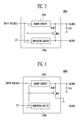
FIG. 3 is a schematic view showing a first embodiment of a DC-DC converter; -
FIG. 4 is a schematic view showing a second embodiment of a DC-DC converter; -
FIG. 5 is a schematic view showing a third embodiment of a DC-DC converter; -
FIG. 6 is a schematic view showing a fourth embodiment of a DC-DC converter; -
FIG. 7 is a schematic view showing a fifth embodiment of a DC-DC converter; and -
FIG. 8 is a schematic view showing a sixth embodiment of a DC-DC converter. - Hereinafter, certain embodiments according to the present invention will be described with reference to the accompanying drawings. Here, when a first element is described as being coupled to a second element, the first element may be not only directly coupled to the second element but may also be indirectly coupled to the second element via a third element. Furthermore, elements that are not essential to the complete understanding of the invention may be omitted for clarity. Also, like reference numerals generally refer to like elements throughout.
- Hereinafter, certain embodiments according to the present invention will be described with reference to the accompanying drawings.
-
FIG. 2 is a schematic view showing an organic light emitting display. Referring toFIG. 2 , an organic light emitting display device comprises apixel unit 100, adata driver 200, ascan driver 300, and a DC-DC converter 400. - The
pixel unit 100 is arranged with a plurality ofpixels 101, therespective pixels 101 comprising organic light emitting diodes (not shown) configured to emit light corresponding to the flow of current therethrough. The pixel units are arranged with n scan lines S1, S2,...,Sn-1, Sn formed in a row direction configured to transmit scan signals and m data lines D1, D2,...,Dm-1, Dm formed in a column direction configured to transmit data signals. Also, thepixel unit 100 is operated by receiving first voltage ELVDD and second voltage ELVSS. Therefore, thepixel 100 displays images by light illuminating the organic light emitting diodes by means of the scan signals, the data signals, the first voltage ELVDD and the second voltage ELVSS. - The
data driver 200 is a means for applying the data signals to thepixel unit 100 and receives video data with red, blue, and green components to generate the data signals. Thedata driver 200 is coupled to the data lines D1, D2,...,Dm-1, Dm of thepixel unit 100 to apply the generated data signals to thepixel unit 100. - The
scan driver 300 is a means for applying the scan signals to thepixel unit 100 and is coupled to the scan lines S1, S2,...,Sn-1, Sn to transmit the scan signals to the particular rows of thepixel unit 100. Thepixels 101, which receive the scan signals, also receive the data signals output from thedata driver 200 to generate driving current from thepixels 101 so that the driving current flows into the organic light emitting diodes of thepixels 101. - The DC-
DC converter 400 is a means for transferring the first voltage ELVDD and the second ELVSS to thepixel unit 100. DC-DC converter 400 converts a received voltage to generate the first voltage ELVDD and the second voltage ELVSS for thepixel unit 100. The DC-DC converter is formed using a regulator and comprises a boost circuit for generating the first voltage ELVDD and an inverter circuit for generating the second voltage ELVSS. -
FIG. 3 is a schematic view showing an embodiment of a DC-DC converter. Referring toFIG. 3 , the DC-DC converter 400a comprises aboost circuit 410a, aninverter circuit 420a, a capacitor Cch, and a switch unit comprising Rch and Mch. - The
boost circuit 410a is a means for receiving an input voltage and is configured to boost the input voltage to generate the first voltage ELVDD. The input voltage may, for example, be from a battery for a mobile phone, etc. - The
inverter circuit 420a is a means for receiving the input voltage and is configured to invert the input voltage to generate the second voltage ELVSS with low voltage. - In addition, the
boost circuit 410a and theinverter circuit 420a receive a control signal CS controlling whether they are operated. - The capacitor Cch is coupled to an output terminal outputting the first voltage ELVDD of the DC-
DC converter 400a, making it possible to stably output the output of the DC-DC converter 400a. - In this embodiment, the switch unit with Rch and Mch is positioned inside the DC-
DC converter 400a and coupled to the capacitor Cch and is configured to discharge or maintain voltage charged in the capacitor Cch according to the control signal CS. - The
boost circuit 410a is stopped by means of the control signal CS, and the capacitor Cch is charged with the voltage of the first power supply ELVDD. Therefore, the voltage of the first power supply ELVDD is transferred to the pixel unit shown inFIG. 2 by means of the charged voltage so that the respective pixels of the pixel unit receive the first voltage ELVDD. Unwanted luminescence of the pixels occurs when the operation of theboost circuit 410a is stopped, shortening the lifetime of the pixels. - Therefore, in order to prevent this unwanted luminescence, the switch unit with Rch and Mch is coupled to the capacitor Cch to produce a path discharging the voltage stored in the capacitor Cch.
- The switch unit comprises the resistor Rch and the transistor Mch. In this embodiment, a first terminal of the resistor Rch is coupled to the output terminal of the
boost circuit 410a and the second terminal is coupled to the source of the transistor Mch. The source of the transistor Mch is coupled to the resistor Rch, the drain thereof is coupled to the output terminal outputting the second voltage ELVSS generated from theinverter circuit 420a, and the gate thereof receives the control signal CS operating the DC-DC converter 400a to perform a switching operation. In some embodiments, the resistor Rch may be connected to the second voltage ELVSS and the transistor Mch may be connected to the output terminal of theboost circuit 410a. - When the DC-
DC converter 400a is operated by means of the control signal CS, the transistor Mch is in an off state and when the operation of the DC-DC converter 400a is stopped, the transistor Mch is in an on state. Therefore, when the transistor Mch is in the on state, the second terminal of the resistor Rch is connected to the second voltage ELVSS to flow the voltage stored in the capacitor Cch into the second power supply ELVSS through the resistor Rch so that the charge stored in the capacitor Cch is conducted through the resistor Rch, in other words to discharge the capacitor Cch. And, when the transistor Mch is in the off state, the current does not flow into the resistor Rch so that it has substantially no effect on the voltage of the output terminal of theboost circuit 410a. - Therefore, when the DC-
DC converter 400a is in the off state, the voltage charged in the capacitor Cch is discharged. As a result, when the DC-DC converter 400a is in the off state, the switch unit prevents the first voltage ELVDD from being transmitted to the pixel unit ofFIG. 2 , making it possible to prevent the respective pixels of the pixel unit from emitting light. -
FIG. 4 is a schematic view showing another embodiment of a DC-DC converter. Referring toFIG. 4 , a DC-DC converter 400b comprises aboost circuit 410b, aninverter circuit 420b, a capacitor Cch, and a switch unit Rch and Mch. - Unlike the DC-
DC converter 400a shown inFIG. 3 , in the DC-DC converter 400b shown inFIG. 4 , one terminal of the transistor Mch of the switch unit Rch and Mch is not coupled to the output terminal of theinverter 420b but is coupled to the ground. Therefore, when theboost circuit 410b is stopped according to the control signal CS, the charge stored in the capacitor Cch flows into the ground through the transistor Mch. - Therefore, when the DC-
DC converter 400b is in an off state, the voltage charged in the capacitor Cch is discharged. As a result, when the DC-DC converter 400b is in the off-state, the switch unit prevents the first voltage ELVDD from being transferred to the pixel unit ofFIG. 2 during predetermined time, making it possible to prevent the respective pixels of the pixel unit from emitting light. -
FIG. 5 is a schematic view showing another embodiment of a DC-DC converter. Referring toFIG. 5 , a DC-DC converter 400c comprises aboost circuit 410c and aninverter circuit 420c and the output terminal of the DC-DC converter 400c is coupled to a capacitor Cch and a switch unit Mch. - The difference between the DC-
DC converter 400c shown inFIG. 5 and the DC-DC converter 400a shown inFIG. 3 is that the transistor Mch is coupled to the output signal outside of the DC-DC converter 400c. - The source of the transistor Mch is coupled to the output terminal of the first power supply ELVDD and the drain thereof is coupled to the ground.
- Therefore, when the
boost circuit 410c is stopped corresponding to the control signal CS, the voltage stored in the capacitor Cch flows into the ground through the transistor Mch. - Accordingly, when the DC-
DC converter 400c is in the off-state, the voltage charged in the capacitor Cch is discharged. As a result, when the DC-DC converter 400c is in the off-state, the transistor Mch prevents the first voltage ELVDD from being transferred to the pixel unit ofFIG. 2 , making it possible to prevent the respective pixels of the pixel unit from emitting light. -
FIG. 6 is a schematic view showing another embodiment of a DC-DC converter. Referring toFIG. 6 , a DC-DC converter 400d comprises aboost circuit 410d and aninverter circuit 420d and the output terminal of the DC-DC converter 400d is coupled to a capacitor Cch and a switch unit and adelay circuit 430 is coupled between the input terminal of the control signal CS and the switch unit. - The
boost circuit 410d is a means for boosting the input voltage to generate the first voltage ELVDD. The input voltage may, for example, be transferred from a battery for a mobile phone, etc. - The
inverter circuit 420d is a means for inverting the input voltage to generate the second voltage ELVSS. - The
boost circuit 410d and theinverter circuit 420d receive a control signal CS to determine whether they are operated. - The capacitor Cch is coupled to the output terminal of the DC-
DC converter 400d, making it possible to stably output the output of the DC-DC converter 400d. - The switch unit is formed outside the DC-
DC converter 400d and discharges voltage charged in the capacitor Cch. When the voltage charged in the capacitor Cch is not discharged and the DC-DC converter 400d is stopped during its operation, the capacitor Cch is charged with the voltage of the first power supply ELVDD. Therefore, the voltage of the first power supply ELVDD is transmitted to the pixel unit shown inFIG. 2 by means of the charged voltage in the capacitor Cch so that the respective pixels of the pixel unit receive the first voltage ELVDD and can emit unwanted light. The luminescence of the pixels shortens the lifetime of the pixels. Therefore, in order to prevent this luminescence, a path for discharging the voltage stored in the capacitor Cch from the switch unit is produced. The switch unit comprises the transistor Mch. The source of the transistor Mch is coupled to the output terminal of theboost circuit 410d, the drain thereof is coupled to the ground, and the gate thereof receives the control signal CS operating the DC-DC converter 400d to perform the switching operation. In other words, when the DC-DC converter 400d is operated by means of the control signal CS, the transistor Mch is in an off state and when the operation of the DC-DC converter 400d is stopped, the transistor Mch is in an on state. When the transistor Mch is in the on state, the charge stored in the capacitor Cch flows into the ground through the transistor Mch to discharge the voltage stored in the capacitor Cch. And, when the transistor Mch is in the off state, the current does not flow so that it has substantially no effect on the voltage of the output terminal of theboost circuit 410d. - In other words, when the DC-
DC converter 400d is in the off state, the voltage charged in the capacitor Cch is discharged. As a result, when the DC-DC converter 400c is in the off state, the switch unit prevents the first voltage ELVDD from being transmitted to the pixel unit ofFIG. 2 , making it possible to prevent the respective pixels of the pixel unit from emitting light. - The
delay circuit 430 is a means for delaying the application of the control signal CS to the transistor Mch. Thedelay circuit 430 turns the transistor Mch on with a delay after the DC-DC converter 400d is stopped. Therefore, the charge in the capacitor Cch does not flow into the ground through the transistor Mch immediately after the operation of the DC-DC converter 400d is stopped but flows into the ground through the transistor Mch after a delay, so that the first power supply ELVDD is not immediately interrupted. -
FIG. 7 is a structure view showing another embodiment of a DC-DC converter. Referring toFIG. 7 , a DC-DC converter 400e comprises aboost circuit 410e and aninverter circuit 420e and the output terminal of the DC-DC converter 400e is coupled to a capacitor Cch and a resistor Rch. - The
boost circuit 410e is a means for boosting an input voltage to generate the first voltage ELVDD. The input voltage may, for example, be transferred from a battery for a mobile phone, etc. - The
inverter circuit 420e is a means for inverting the input voltage to generate the second voltage ELVSS. - The
boost circuit 410e and theinverter circuit 420e receive a control signal CS to determine whether they are operated. - The capacitor Cch is coupled to the output terminal of the DC-
DC converter 400e, making it possible to stably output the output of the DC-DC converter 400e. - In this embodiment, the resistor Rch is formed outside the DC-
DC converter 400e and discharges charge in the capacitor Cch. When the voltage charged in the capacitor Cch is not discharged and the DC-DC converter 400e is stopped during its operation, the capacitor Cch is charged with the voltage of the first power supply ELVDD. Therefore, the voltage of the first power supply ELVDD is transmitted to the pixel unit shown inFIG. 2 through theboost circuit 410e so that the respective pixels of the pixel unit receive the first voltage ELVDD and can emit light. The luminescence of the pixels occurs in a state where the operation of the DC-DC converter 400e is stopped, having a bad effect on the lifetime of the pixels, etc. Therefore, in order to prevent this luminescence, a path discharging the capacitor Cch through the resistor Rch is produced. The one terminal of the resistor Rch is coupled to the output terminal of the DC-DC converter 400e and the other terminal thereof is coupled to the ground. Accordingly, the voltage charged in the capacitor Cch is dissipated through the resistor Rch. Since the time of discharging the voltage charged in the capacitor Cch corresponds to the size of the capacitor Cch and the size of the resistor Rch, the sizes of the capacitor Cch and the resistor Rch are controlled, preventing the voltage charged in the capacitor Cch from discharging too fast or too slow. - Because the voltage stored at the output terminal of the DC-
DC converter 400e is discharged after the DC-DC converter 400e is in the off state, the voltage of the first power supply ELVDD is prevented from being transmitted to the pixel unit ofFIG. 2 , making it possible to prevent the respective pixels of the pixel unit from emitting light. -
FIG. 8 is a structure view showing another embodiment of a DC-DC converter. Referring toFIG. 8 , the DC-DC converter 400f comprises aboost circuit 410f and aninverter circuit 420f and the output terminal of the DC-DC converter 400f is coupled to capacitors Cch1 and Cch2 and a resistor Rch. - The
boost circuit 410f is a means for boosting an input voltage to generate the first voltage ELVDD. The input voltage may, for example, be transmitted from a battery for a mobile phone, etc. - The
inverter circuit 420f is a means for inverting the input voltage to generate the second voltage ELVSS. - The
boost circuit 410f and theinverter circuit 420f receive a control signal CS to determine whether they are operated. - The capacitors Cch1 and Cch2 are coupled to the output terminals of the
boost circuit 410f and theinverter circuit 420f, respectively, making it possible to stably output the voltage of the first power supply ELVDD and the voltage of the second power supply ELVSS. - The resistor Rch is formed outside the DC-
DC converter 400f and discharges voltage charged in the capacitors Cch1 and Cch2. When the voltages charged in the capacitors Cch1 and Cch2 are not discharged and the DC-DC converter 400f is stopped during its operation, the capacitors Cch1 and Cch2 are charged with the voltage of the first power supply ELVDD and the second power supply ELVSS, respectively. Therefore, the voltage of the first power supply ELVDD and the second power supply ELVSS are transferred to the pixel unit shown inFIG. 2 so that the respective pixels of the pixel unit can emit light. The luminescence of the pixels occurs in a state where the operation of the DC-DC converter 400f is stopped, having a bad effect on the lifetime of the pixels, etc. Therefore, in order to prevent this luminescence, a path discharging the voltage stored in the capacitors Cch1 and Cch2 through the resistor Rch is produced. The one terminal of the resistor Rch is coupled to the output terminal of theboost circuit 410f and the other terminal thereof is coupled to the output terminal of theinverter circuit 420f. Accordingly, the resistor Rch is positioned between the voltage of the first power supply ELVDD and the voltage of the second power supply ELVSS to discharge the capacitors Cch1 and Cch2. Since the time discharging the voltages charged in the capacitors Cch1 and Cch2 corresponds to the sizes of the capacitors Cch1 and Cch2 and the size of the resistor Rch, the sizes of the capacitors Cch1 and Cch2 and the resistor Rch are controlled, preventing the voltages charged in the capacitors Cch1 and Cch2 from being discharged too fast or too slow. - Because the voltage stored in the output terminal of the DC-
DC converter 400f is discharged after the DC-DC converter 400f is in the off state, the voltage stored in the output terminals of the DC-DC converter 400f are prevented from being transmitted to the pixel unit ofFIG. 2 , making it possible to prevent the respective pixels of the pixel unit from emitting light. - With the DC-DC converter and the organic light emitting display using the same according to the present invention, the harmful luminescence phenomenon caused due to the application of the first voltage ELVDD and the second voltage ELVSS to the pixels when the DC-DC converter is turned-off can be prevented.
- Although certain embodiments of the present invention have been shown and described, it would be appreciated by those skilled in the art that changes might be made in this embodiment without departing from the scope of the invention as defined in the appended claims.
Claims (13)
- A DC-DC converter (400, 400a - f) comprising:a voltage generator configured to receive an input voltage through an input terminal, and to generate a first output voltage and a second output voltage, the second output voltage being less than the first output voltage, and to output the first output voltage and second output voltage through first and second output terminals, respectively, wherein the voltage generator is configured to generate the first and second output voltages according to a control signal (CS);a capacitor (Cch, Cch1, Cch2) coupled to at least one of the first and second output terminals; andmeans (Rch, Mch) configured to selectively discharge the capacitor.
- The DC-DC converter as claimed in claim 1, wherein the selective discharge means is arranged to discharge the capacitor when the first ouput voltage is arranged not to be generated.
- The DC-DC converter as claimed in claim 1 or 2, wherein the voltage generator further comprises a boost circuit (410a-f) configured to generate the first output voltage; and
an inverter circuit (420a-f) configured to generate the second output voltage. - The DC-DC converter as claimed in any one of the preceding claims, wherein the selective discharge means comprises a switch unit (Mch) configured to selectively discharge the capacitor in accordance with the control signal.
- The DC-DC converter as claimed in claim 4, wherein the switch unit further comprises a transistor (Mch) configured to be turned on and off by the control signal (CS).
- The DC-DC converter as claimed in claim 5, further comprising a resistor (Rch) selectively connected to the capacitor by the transistor and configured to discharge the capacitor.
- The DC-DC converter as claimed in claim 5 or 6, further comprising a delay circuit (430) configured to receive the control signal and to transmit the control signal to the gate of the transistor after a delay.
- The DC-DC converter as claimed in any one of claims 5 to 7, wherein the transistor is coupled to a ground.
- The DC-DC converter as claimed in claim 3, wherein the transistor is coupled to the second output voltage.
- The DC-DC converter (400e, 400f) as claimed in any one of claims 1 to 3, wherein the selective discharge means comprises a resistor (Rch) configured to selectively discharge the capacitor (Cch) when the first output voltage is arranged not to be generated.
- The DC-DC converter as claimed in claim 10, further comprising a second capacitor (CCh2) coupled to the other of the first and second output terminals.
- The DC-DC converter as claimed in claim 11, wherein the resistor is coupled to both of the first and second output terminals.
- An organic light emitting display comprising:a pixel unit configured to display images based on received data signals, scan signals, and first and second voltages;a data driver configured to generate the data signals;a scan driver configured to generate the scan signals; anda DC-DC converter according to any one of the preceding claims configured to generate the first and second voltages.
Applications Claiming Priority (1)
| Application Number | Priority Date | Filing Date | Title |
|---|---|---|---|
| KR1020070086511A KR100889690B1 (en) | 2007-08-28 | 2007-08-28 | Converter and organic light emitting display thereof |
Publications (2)
| Publication Number | Publication Date |
|---|---|
| EP2031941A2 true EP2031941A2 (en) | 2009-03-04 |
| EP2031941A3 EP2031941A3 (en) | 2012-01-11 |
Family
ID=40092049
Family Applications (1)
| Application Number | Title | Priority Date | Filing Date |
|---|---|---|---|
| EP08163107A Withdrawn EP2031941A3 (en) | 2007-08-28 | 2008-08-27 | DC-DC converter and organic light emitting display using the same |
Country Status (5)
| Country | Link |
|---|---|
| US (1) | US8749462B2 (en) |
| EP (1) | EP2031941A3 (en) |
| JP (1) | JP4659807B2 (en) |
| KR (1) | KR100889690B1 (en) |
| CN (1) | CN101378229A (en) |
Cited By (3)
| Publication number | Priority date | Publication date | Assignee | Title |
|---|---|---|---|---|
| EP2357634A2 (en) * | 2009-11-17 | 2011-08-17 | Samsung Mobile Display Co., Ltd. | DC-DC converter and organic light emitting display device using the same |
| EP3065277A1 (en) * | 2015-03-03 | 2016-09-07 | Samsung Display Co., Ltd. | Dc-dc converter and display device having the same |
| US9799298B2 (en) | 2010-04-23 | 2017-10-24 | Semiconductor Energy Laboratory Co., Ltd. | Liquid crystal display device and driving method thereof |
Families Citing this family (20)
| Publication number | Priority date | Publication date | Assignee | Title |
|---|---|---|---|---|
| JP4502003B2 (en) * | 2007-12-26 | 2010-07-14 | エプソンイメージングデバイス株式会社 | Electro-optical device and electronic apparatus including the electro-optical device |
| KR100952834B1 (en) * | 2008-08-06 | 2010-04-15 | 삼성모바일디스플레이주식회사 | Dc-dc converter and organic light emitting display using the same |
| JP5515331B2 (en) | 2009-03-09 | 2014-06-11 | ソニー株式会社 | Information providing server, information providing system, information providing method, and program |
| KR101049019B1 (en) | 2009-05-19 | 2011-07-12 | 삼성모바일디스플레이주식회사 | Power supply unit and organic light emitting display device using the same |
| KR101067225B1 (en) * | 2009-07-08 | 2011-09-22 | 삼성전기주식회사 | On/Off Sequence Circuit for Using Plasma Display Panel |
| KR101022085B1 (en) | 2009-07-10 | 2011-03-17 | 삼성모바일디스플레이주식회사 | Power supply and organic light emitting display device using the same |
| KR101084170B1 (en) * | 2009-08-03 | 2011-11-17 | 삼성모바일디스플레이주식회사 | Power control system for display module with external DC-DC convertor |
| KR101064462B1 (en) | 2009-11-17 | 2011-09-15 | 삼성모바일디스플레이주식회사 | Dc-dc converter and organic light emitting display device for the same |
| KR101132023B1 (en) | 2010-02-19 | 2012-04-02 | 삼성모바일디스플레이주식회사 | Dc-dc converter and organic light emitting display using the same |
| KR101193194B1 (en) * | 2010-04-30 | 2012-10-19 | 삼성디스플레이 주식회사 | Organic Light Emitting Display |
| KR101992281B1 (en) * | 2012-03-06 | 2019-06-26 | 삼성디스플레이 주식회사 | Organic Light Emitting Display and Driving Method Thereof |
| KR101975531B1 (en) * | 2012-09-10 | 2019-05-08 | 삼성디스플레이 주식회사 | Organic Light Emitting Display Device and Driving Method Thereof |
| KR102071004B1 (en) | 2013-09-03 | 2020-01-30 | 삼성디스플레이 주식회사 | Dc-dc converter and organic light emitting display including the same |
| KR102141207B1 (en) * | 2013-11-11 | 2020-08-05 | 삼성디스플레이 주식회사 | Display apparatus, power voltage generating apparatus, and method for generating power voltage |
| KR102484869B1 (en) * | 2015-12-02 | 2023-01-06 | 엘지디스플레이 주식회사 | Organic light emitting display device and method for driving organic light emitting display device |
| KR102430795B1 (en) * | 2015-12-31 | 2022-08-08 | 엘지디스플레이 주식회사 | Display device and method for driving the same |
| CN105657898B (en) | 2016-02-19 | 2017-12-08 | 京东方科技集团股份有限公司 | A kind of power circuit and its driving method, display device |
| CN107103871B (en) * | 2017-06-30 | 2019-11-22 | 京东方科技集团股份有限公司 | The power supply circuit and method of supplying power to of display device and display screen |
| CN110544452B (en) * | 2018-05-28 | 2021-08-17 | 京东方科技集团股份有限公司 | Power supply time sequence control circuit and control method, display driving circuit and display device |
| KR102519570B1 (en) | 2018-11-12 | 2023-04-10 | 삼성디스플레이 주식회사 | Display apparatus and method of driving display panel using the same |
Citations (2)
| Publication number | Priority date | Publication date | Assignee | Title |
|---|---|---|---|---|
| US20030184538A1 (en) * | 2002-04-02 | 2003-10-02 | Asahi Yamato | Power source apparatus for display and image display apparatus |
| US20060181904A1 (en) | 2005-02-16 | 2006-08-17 | Samsung Electronics Co., Ltd. | Driving apparatus of display device and DC-DC converter |
Family Cites Families (21)
| Publication number | Priority date | Publication date | Assignee | Title |
|---|---|---|---|---|
| US4422073A (en) * | 1981-10-27 | 1983-12-20 | The Bendix Corporation | Combustible gas detection system |
| CN1023048C (en) | 1989-08-17 | 1993-12-08 | 哈尔滨工业大学 | Phase cut-off protector of phase and width discrimination |
| JPH05236744A (en) * | 1992-02-19 | 1993-09-10 | Ricoh Co Ltd | Multioutput swtching power source unit |
| JP2000152623A (en) | 1998-11-10 | 2000-05-30 | Ricoh Co Ltd | Power unit |
| GB9921425D0 (en) | 1999-09-11 | 1999-11-10 | Koninkl Philips Electronics Nv | Active matrix electroluminescent display device |
| KR100389019B1 (en) * | 2000-11-22 | 2003-06-25 | 엘지전자 주식회사 | Reset Circuit in Plasma Display Panel |
| JP2002233139A (en) | 2001-02-05 | 2002-08-16 | Matsushita Electric Ind Co Ltd | Dc-dc converter |
| JP2002244617A (en) * | 2001-02-15 | 2002-08-30 | Sanyo Electric Co Ltd | Organic el pixel circuit |
| JP3788916B2 (en) | 2001-03-30 | 2006-06-21 | 株式会社日立製作所 | Light-emitting display device |
| KR100878222B1 (en) | 2001-07-03 | 2009-01-13 | 삼성전자주식회사 | Apparatus for supplying power for a liquid crystal display |
| US7483001B2 (en) | 2001-11-21 | 2009-01-27 | Seiko Epson Corporation | Active matrix substrate, electro-optical device, and electronic device |
| KR100514185B1 (en) * | 2003-10-01 | 2005-09-13 | 삼성에스디아이 주식회사 | DC-DC Converter for electro luminescence display |
| US6913554B2 (en) * | 2003-10-03 | 2005-07-05 | Gilbert W. Younger | Methods and systems for improving the operation of transmissions for motor vehicles |
| KR20050046927A (en) * | 2003-11-14 | 2005-05-19 | 삼성에스디아이 주식회사 | Power supply and light emitting display device using the power supply |
| GB0400213D0 (en) | 2004-01-07 | 2004-02-11 | Koninkl Philips Electronics Nv | Electroluminescent display devices |
| JP4803629B2 (en) * | 2004-04-27 | 2011-10-26 | 東北パイオニア株式会社 | Light emitting display device and drive control method thereof |
| KR100662981B1 (en) * | 2004-11-04 | 2006-12-28 | 삼성에스디아이 주식회사 | Light emitting display and DC-DC converter thereof |
| CN100486089C (en) | 2004-12-25 | 2009-05-06 | 鸿富锦精密工业(深圳)有限公司 | Switching power supply |
| JP4984391B2 (en) * | 2005-01-07 | 2012-07-25 | カシオ計算機株式会社 | Display drive device, display device, and drive control method thereof |
| KR100649508B1 (en) * | 2005-02-02 | 2006-11-27 | 권오영 | Hybrid power supply system |
| KR20080064564A (en) * | 2007-01-05 | 2008-07-09 | 삼성전자주식회사 | Printed circuit board and liquid crystal display device having the same |
-
2007
- 2007-08-28 KR KR1020070086511A patent/KR100889690B1/en active IP Right Grant
- 2007-10-23 JP JP2007275362A patent/JP4659807B2/en active Active
-
2008
- 2008-07-08 US US12/217,817 patent/US8749462B2/en active Active
- 2008-08-26 CN CNA2008102124427A patent/CN101378229A/en active Pending
- 2008-08-27 EP EP08163107A patent/EP2031941A3/en not_active Withdrawn
Patent Citations (2)
| Publication number | Priority date | Publication date | Assignee | Title |
|---|---|---|---|---|
| US20030184538A1 (en) * | 2002-04-02 | 2003-10-02 | Asahi Yamato | Power source apparatus for display and image display apparatus |
| US20060181904A1 (en) | 2005-02-16 | 2006-08-17 | Samsung Electronics Co., Ltd. | Driving apparatus of display device and DC-DC converter |
Cited By (4)
| Publication number | Priority date | Publication date | Assignee | Title |
|---|---|---|---|---|
| EP2357634A2 (en) * | 2009-11-17 | 2011-08-17 | Samsung Mobile Display Co., Ltd. | DC-DC converter and organic light emitting display device using the same |
| US9799298B2 (en) | 2010-04-23 | 2017-10-24 | Semiconductor Energy Laboratory Co., Ltd. | Liquid crystal display device and driving method thereof |
| EP3065277A1 (en) * | 2015-03-03 | 2016-09-07 | Samsung Display Co., Ltd. | Dc-dc converter and display device having the same |
| US10504434B2 (en) | 2015-03-03 | 2019-12-10 | Samsung Display Co., Ltd. | DC-DC converter and display device having the same |
Also Published As
| Publication number | Publication date |
|---|---|
| CN101378229A (en) | 2009-03-04 |
| KR100889690B1 (en) | 2009-03-19 |
| US20090058311A1 (en) | 2009-03-05 |
| JP4659807B2 (en) | 2011-03-30 |
| EP2031941A3 (en) | 2012-01-11 |
| JP2009055774A (en) | 2009-03-12 |
| KR20090021742A (en) | 2009-03-04 |
| US8749462B2 (en) | 2014-06-10 |
Similar Documents
| Publication | Publication Date | Title |
|---|---|---|
| EP2031941A2 (en) | DC-DC converter and organic light emitting display using the same | |
| US7561128B2 (en) | Organic electroluminescence display device | |
| US8803769B2 (en) | DC-DC converter and organic light emitting display using the same | |
| US8564587B2 (en) | Organic light emitting diode display | |
| US9041626B2 (en) | Organic light emitting display and power supply method thereof | |
| US8482492B2 (en) | Organic light emitting display with an improved emission control driver and method of driving the same | |
| US8411077B2 (en) | DC-DC converter and organic light emitting display device using the same | |
| US9799269B2 (en) | Pixel circuit, display panel and driving method thereof | |
| US8665182B2 (en) | Emission control driver and organic light emitting display device using the same | |
| US20060208975A1 (en) | Display apparatus | |
| EP2128848A1 (en) | Pixel and organic light emiting display using the same | |
| CN107784974B (en) | Display device and driving method thereof | |
| US8791886B2 (en) | DC-DC converter and organic light emitting display device including the same | |
| US20100128021A1 (en) | Pixel and organic light emitting display device using the same | |
| US9852690B2 (en) | Drive method and display device | |
| US8817003B2 (en) | Power supply unit and organic light emitting display device using the same | |
| US8223140B2 (en) | Organic electroluminescent display and power supply device for the same | |
| KR20090093019A (en) | Dc-dc converter and organic light emitting display thereof | |
| US7133010B2 (en) | Method and apparatus for data-driving electro-luminescence display panel device | |
| KR20130086876A (en) | Organic light emitting display device and driving method thereof | |
| KR100343371B1 (en) | Active matrix organic EL display device and driving method thereof | |
| US8570309B2 (en) | Buffer and organic light emitting display using the same | |
| KR100520829B1 (en) | Driving Apparatus And Method For Electro-Luminescence Display Panel |
Legal Events
| Date | Code | Title | Description |
|---|---|---|---|
| PUAI | Public reference made under article 153(3) epc to a published international application that has entered the european phase |
Free format text: ORIGINAL CODE: 0009012 |
|
| 17P | Request for examination filed |
Effective date: 20080827 |
|
| AK | Designated contracting states |
Kind code of ref document: A2 Designated state(s): AT BE BG CH CY CZ DE DK EE ES FI FR GB GR HR HU IE IS IT LI LT LU LV MC MT NL NO PL PT RO SE SI SK TR |
|
| AX | Request for extension of the european patent |
Extension state: AL BA MK RS |
|
| RAP1 | Party data changed (applicant data changed or rights of an application transferred) |
Owner name: SAMSUNG MOBILE DISPLAY CO., LTD. |
|
| PUAL | Search report despatched |
Free format text: ORIGINAL CODE: 0009013 |
|
| AK | Designated contracting states |
Kind code of ref document: A3 Designated state(s): AT BE BG CH CY CZ DE DK EE ES FI FR GB GR HR HU IE IS IT LI LT LU LV MC MT NL NO PL PT RO SE SI SK TR |
|
| AX | Request for extension of the european patent |
Extension state: AL BA MK RS |
|
| RIC1 | Information provided on ipc code assigned before grant |
Ipc: H05B 33/08 20060101AFI20111207BHEP Ipc: G09G 3/32 20060101ALN20111207BHEP |
|
| AKX | Designation fees paid |
Designated state(s): DE FR GB HU |
|
| RAP1 | Party data changed (applicant data changed or rights of an application transferred) |
Owner name: SAMSUNG DISPLAY CO., LTD. |
|
| RAP1 | Party data changed (applicant data changed or rights of an application transferred) |
Owner name: SAMSUNG DISPLAY CO., LTD. |
|
| 17Q | First examination report despatched |
Effective date: 20170113 |
|
| STAA | Information on the status of an ep patent application or granted ep patent |
Free format text: STATUS: THE APPLICATION IS DEEMED TO BE WITHDRAWN |
|
| 18D | Application deemed to be withdrawn |
Effective date: 20171201 |