JP4655497B2 - Pixel circuit driving method, pixel circuit, electro-optical device, and electronic apparatus - Google Patents
Pixel circuit driving method, pixel circuit, electro-optical device, and electronic apparatus Download PDFInfo
- Publication number
- JP4655497B2 JP4655497B2 JP2004109210A JP2004109210A JP4655497B2 JP 4655497 B2 JP4655497 B2 JP 4655497B2 JP 2004109210 A JP2004109210 A JP 2004109210A JP 2004109210 A JP2004109210 A JP 2004109210A JP 4655497 B2 JP4655497 B2 JP 4655497B2
- Authority
- JP
- Japan
- Prior art keywords
- data
- capacitor
- drive
- current
- transistor
- Prior art date
- Legal status (The legal status is an assumption and is not a legal conclusion. Google has not performed a legal analysis and makes no representation as to the accuracy of the status listed.)
- Expired - Fee Related
Links
Images


Description
本発明は、画素回路の駆動方法、画素回路、電気光学装置および電子機器に係り、特に
、画素回路の差分駆動に関する。
The present invention relates to a pixel circuit driving method, a pixel circuit, an electro-optical device, and an electronic apparatus, and more particularly to differential driving of a pixel circuit.
近年、有機EL(Electronic Luminescence)素子を用いたフラットパネルディスプレ
イ(FPD)が注目されている。有機EL素子は、自己を流れる駆動電流によって駆動す
る電流駆動型素子の一つであり、その電流レベルに応じた輝度で自ら発光する。このよう
な素子を有する画素回路のデータ書込方式には、電流プログラム方式と電圧プログラム方
式とがある。電流プログラム方式は、画素回路が接続されたデータ線に対するデータの供
給を電流ベースで行う方式であり、電圧プログラム方式は、このデータ供給を電圧ベース
で行う方式である。
In recent years, flat panel displays (FPD) using organic EL (Electronic Luminescence) elements have attracted attention. The organic EL element is one of current-driven elements that are driven by a drive current that flows through the organic EL element, and emits light with a luminance corresponding to the current level. There are a current programming method and a voltage programming method as a data writing method for a pixel circuit having such an element. The current program method is a method in which data is supplied to the data lines connected to the pixel circuits on a current basis, and the voltage program method is a method in which this data supply is performed on a voltage basis.
特許文献1には、前回のフレームにおける表示画像信号と、今回のフレームにおけるそ
れとの差分信号を入力とし、これらを合成したアナログ的な階調データを画素回路に出力
することにより、低消費電力化を図る液晶表示装置が開示されている。
特許文献1でにおいて、データ線駆動回路からデータ線を介して画素回路に供給される
階調データは、走査毎に完全に更新されるため、十分な低消費電力化を図ることが困難で
ある。
In
本発明の目的は、画素回路の新規な駆動制御を提供することである。 An object of the present invention is to provide a novel drive control of a pixel circuit.
また、本発明の別の目的は、画素回路の駆動における消費電力の低減を図ることである
。
Another object of the present invention is to reduce power consumption in driving a pixel circuit.
かかる課題を解決するために、第1の発明は、第1のフレームでデータ線より供給された第1のデータを保持するとともに、保持されたデータに応じた第1の駆動電流を生成する一方の駆動系と、第1のフレームの後の第2のフレームでデータ線より供給され、第2のフレームにおける階調を規定する階調データと、第1のデータとの差分に相当する差分データを第2のデータとして保持するとともに、保持されたデータに応じた第2の駆動電流を生成する他方の駆動系と、第2のフレームにおいて、第1の駆動電流と第2の駆動電流とを合成した合成電流を供給することによって、階調データ相当の輝度に設定される電気光学素子とを有する画素回路を提供する。 In order to solve such a problem, the first invention holds the first data supplied from the data line in the first frame and generates the first drive current corresponding to the held data. The difference data corresponding to the difference between the first data and the drive data and the gradation data supplied from the data line in the second frame after the first frame and defining the gradation in the second frame As the second data, and the other drive system that generates the second drive current according to the held data, and the first drive current and the second drive current in the second frame Provided is a pixel circuit having an electro-optic element that is set to a luminance equivalent to gradation data by supplying a synthesized current.
ここで、第1の発明において、他方の駆動系は、第2のデータを保持する第1のキャパシタと、第1のキャパシタに自己のゲートが接続されているとともに、第1のキャパシタに保持されたデータに応じて、第2の駆動電流の少なくとも一部となる第2の順駆動電流を生成する第1の駆動素子と、第2のデータを保持する第2のキャパシタと、第2のキャパシタに自己のゲートが接続されているとともに、第2のキャパシタに保持されたデータに応じて、第2の駆動電流の少なくとも一部となり、かつ、第2の順駆動電流とは逆向きの第2の逆駆動電流を生成する第2の駆動素子とを有することが好ましい。 Here, in the first invention , the other drive system includes a first capacitor that holds the second data, a gate connected to the first capacitor, and is held by the first capacitor. A first drive element that generates a second forward drive current that is at least a part of the second drive current according to the data, a second capacitor that holds the second data, and a second capacitor Is connected to the gate of the second capacitor, and at least a part of the second drive current according to the data held in the second capacitor, and is opposite to the second forward drive current. It is preferable to have the 2nd drive element which produces | generates reverse drive current of this.
第1の発明において、第1のデータは、第1のフレームにおける階調を規定する階調データと、第1のフレームの前の第3のフレームにおける差分データとの差分に相当する差分データであってもよい。この場合、一方の駆動系は、第1のデータを保持する第3のキャパシタと、第3のキャパシタに自己のゲートが接続されているとともに、第3のキャパシタに保持されたデータに応じて、第1の駆動電流の少なくとも一部となる第1の順駆動電流を生成する第3の駆動素子と、第1のデータを保持する第4のキャパシタと、第4のキャパシタに自己のゲートが接続されているとともに、第4のキャパシタに保持されたデータに応じて、第1の駆動電流の少なくとも一部となり、かつ、第1の順駆動電流とは逆向きの第1の逆駆動電流を生成する第4の駆動素子とを有することが好ましい。 In the first invention , the first data is difference data corresponding to the difference between the gradation data defining the gradation in the first frame and the difference data in the third frame before the first frame. There may be. In this case, one of the drive systems has a third capacitor that holds the first data, a gate connected to the third capacitor, and the data held in the third capacitor, A third drive element that generates a first forward drive current that is at least part of the first drive current, a fourth capacitor that holds the first data, and a gate connected to the fourth capacitor And generates a first reverse drive current that is at least part of the first drive current and is opposite to the first forward drive current in accordance with the data held in the fourth capacitor. And a fourth driving element.
また、第1のデータは、第1のフレームにおける階調を規定する階調データであってもよい。この場合、一方の駆動系は、第1のデータを保持する第3のキャパシタと、第3のキャパシタに自己のゲートが接続されているとともに、第3のキャパシタに保持されたデータに応じて、第1の駆動電流を生成する第3の駆動素子とを有することが好ましい。 Further, the first data may be gradation data that defines the gradation in the first frame. In this case, one of the drive systems has a third capacitor that holds the first data, a gate connected to the third capacitor, and the data held in the third capacitor, It is preferable to have a third drive element that generates the first drive current.
第1の発明において、データ線に供給された電圧レベルの第1のデータを一方の駆動系に含まれるキャパシタの一方の電極に選択的に供給する第1のスイッチング素子と、データ線に供給された電圧レベルの第2のデータを他方の駆動系に含まれるキャパシタの一方の電極に選択的に供給する第2のスイッチング素子とをさらに設けてもよい。 In the first invention , the first switching element for selectively supplying the first data of the voltage level supplied to the data line to one electrode of the capacitor included in one drive system, and the first switching element supplied to the data line There may be further provided a second switching element that selectively supplies the second data of the voltage level to one electrode of the capacitor included in the other drive system.
第1の発明において、第1の駆動素子を選択的にダイオード接続して、データ線に供給された電流レベルの第1のデータを一方の駆動系に含まれる駆動素子のチャネルに供給する第1のスイッチング素子と、第2の駆動素子を選択的にダイオード接続して、データ線に供給された電流レベルの第2のデータを他方の駆動系に含まれる駆動素子のチャネルに供給する第2のスイッチング素子とをさらに設けてもよい。 In the first invention , the first driving element is selectively diode-connected, and the first data of the current level supplied to the data line is supplied to the channel of the driving element included in one driving system. The switching element and the second driving element are selectively diode-connected, and the second data of the current level supplied to the data line is supplied to the channel of the driving element included in the other driving system. A switching element may be further provided.
第2の発明は、複数の走査線と、複数のデータ線と、走査線とデータ線との交差に対応して設けられた複数の画素回路と、走査線に走査信号を出力することにより、データの書込対象となる画素回路に対応する走査線を選択する走査線駆動回路と、走査線駆動回路と協働し、書込対象となる画素回路に対応するデータ線にデータを出力するデータ線駆動回路とを有する電気光学装置を提供する。ここで、画素回路は、上述した第1の発明にかかる画素回路である。 The second invention provides a plurality of scanning lines, a plurality of data lines, a plurality of pixel circuits provided corresponding to the intersection of the scanning lines and the data lines, and a scanning signal output to the scanning lines, A scanning line driving circuit for selecting a scanning line corresponding to a pixel circuit to which data is to be written, and data for outputting data to a data line corresponding to the pixel circuit to be written in cooperation with the scanning line driving circuit. An electro-optical device having a line driving circuit is provided. Here, the pixel circuit is the pixel circuit according to the first invention described above.
第3の発明は、上記第2の発明にかかる電気光学装置を実装した電子機器を提供する。 A third invention provides an electronic apparatus in which the electro-optical device according to the second invention is mounted.
第4の発明は、一方の駆動系に含まれるキャパシタに、第1のフレームでデータ線より供給された第1のデータを保持する第1のステップと、他方の駆動系に含まれるキャパシタに、第1のフレームの後の第2のフレームでデータ線より供給され、第2のフレームにおける階調を規定する階調データと、第1のデータとの差分に相当する差分データを第2のデータとして保持する第2のステップと、第2のフレームにおいて、一方の駆動系に含まれる駆動素子が第1のデータに応じた第1の駆動電流を生成し、他方の駆動系に含まれる駆動素子が第2のデータに応じた第2の駆動電流を生成するとともに、第1の駆動電流と第2の駆動電流とを合成した合成電流を電気光学素子に供給することによって、電気光学素子の輝度を階調データ相当に設定する第3のステップとを有する画素回路の駆動方法を提供する。 According to a fourth aspect of the present invention, there is provided a first step of holding the first data supplied from the data line in the first frame in the capacitor included in one drive system, and a capacitor included in the other drive system. Difference data corresponding to the difference between the first data and the gradation data supplied from the data line in the second frame after the first frame and defining the gradation in the second frame is the second data. In the second step and the second frame, the drive element included in one drive system generates a first drive current according to the first data, and the drive element included in the other drive system Generates a second drive current according to the second data, and supplies a combined current obtained by combining the first drive current and the second drive current to the electro-optic element, whereby the luminance of the electro-optic element Is equivalent to gradation data To provide a method of driving a pixel circuit having a third step of setting.
ここで、第4の発明において、第1のデータは、第1のフレームの前の第3のフレームにおける差分データと、第1のフレームにおける階調を規定する階調データとの差分に相当する差分データであってもよい。また、第1のデータは、第1のフレームにおける階調を規定する階調データであってもよい。 Here, in the fourth invention , the first data corresponds to a difference between the difference data in the third frame before the first frame and the gradation data defining the gradation in the first frame. It may be difference data. Further, the first data may be gradation data that defines the gradation in the first frame.
本発明では、画素回路に複数の駆動系を設け、それぞれの駆動系に対してデータを交互
に供給するとともに、これらの駆動系の合成電流に基づいて電気光学素子の輝度を設定す
る。これにより、画素回路の駆動における低消費電力化を図ることが可能になる。
In the present invention, a plurality of drive systems are provided in the pixel circuit, and data is alternately supplied to each drive system, and the luminance of the electro-optical element is set based on the combined current of these drive systems. Thereby, it is possible to reduce power consumption in driving the pixel circuit.
(第1の実施形態)
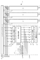
図1は、本実施形態にかかる電気光学装置のブロック構成図である。表示部1は、例え
ばTFT(Thin Film Transistor)によって電気光学素子を駆動するアクティブマトリク
ス型の表示パネルである。この表示部1には、mドット×nライン分の画素群がマトリク
ス状(二次元平面的)に並んでいる。表示部1には、それぞれが水平方向に延在している
走査線群Y1〜Ynと、それぞれが垂直方向に延在しているデータ線群X1〜Xmとが設けら
れており、これらの交差に対応して画素2(後述する画素回路)が配置されている。なお
、後述する各画素回路との関係で、同図に示した1本の走査線Yが複数の走査線のセット
を示すことがあり、同図に示した1本のデータ線Xが複数のデータ線のセットを示すこと
がある。
(First embodiment)
FIG. 1 is a block diagram of the electro-optical device according to the present embodiment. The
制御回路5は、図示しない上位装置からの外部信号をベースに、後述するST、CLX
、φ、LP等を含む各種の内部信号を生成し、これらに基づいて、走査線駆動回路3とデ
ータ線駆動回路4とを同期制御する。この同期制御の下、これらの駆動回路3,4は互い
に協働して、表示部1の表示制御を行う。走査線駆動回路3は、シフトレジスタ、出力回
路等を主体に構成されており、走査線Y1〜Ynに走査信号SELを出力する。走査信号S
ELは、高電位レベル(以下「Hレベル」という)または低電位レベル(以下「Lレベル
」という)の2値的な信号レベルをとり、データの書込対象となる画素行に対応する走査
線YはHレベル、これ以外の走査線YはLレベルにそれぞれ設定される。走査線駆動回路
3は、1画像の表示期間に相当する1フレーム(1F)毎に、所定の選択順序で(一般的
には最上から最下に向かって)、それぞれの走査線Yを順番に選択する線順次走査を行う
。
The
, Φ, LP, and the like are generated, and the scanning
EL takes a binary signal level of a high potential level (hereinafter referred to as “H level”) or a low potential level (hereinafter referred to as “L level”), and is a scanning line corresponding to a pixel row to which data is to be written. Y is set to the H level, and the other scanning lines Y are set to the L level. The scanning
データ線駆動回路4は、走査線駆動回路3による線順次走査と同期して、それぞれのデ
ータ線X1〜Xmにデータを出力する。この出力データは、画素2の階調を規定する階調デ
ータDそのものではなく、隣接したフレーム間における「差分データΔD」(実際には、
これをアナログ化した信号)である。本実施形態において、i番目のフレームFiの「差
分データΔDi」は、その直前フレームFi-1の差分データΔDi-1と、フレームFiの階調
データDiとの差分値(Di−ΔDi-1)として定義される。この定義に従えば、階調デー
タDiと差分データΔDiとの関係は、例えば下記のようになる。差分データΔDiは、正
負を伴うので、階調データDiのビット数(例えば6ビット)に正負を指す1ビットを加
えたビット数(例えば7ビット)が必要となる。
The data
This is an analog signal). In this embodiment, “difference data ΔDi” of the i-th frame Fi is the difference value (Di−ΔDi−1) between the difference data ΔDi−1 of the immediately preceding frame Fi−1 and the gradation data Di of the frame Fi. Is defined as According to this definition, the relationship between the gradation data Di and the difference data ΔDi is, for example, as follows. Since the difference data ΔDi involves both positive and negative, a bit number (for example, 7 bits) obtained by adding one bit indicating positive / negative to the bit number (for example, 6 bits) of the gradation data Di is required.
(階調データと差分データとの関係)
フレームFi F1 F2 F3 F4 F5 ・・・
階調データDi 100 120 200 150 80 ・・・
差分データΔDi +100 +20 +180 -30 +110 ・・・
(Relation between gradation data and difference data)
Frame Fi F1 F2 F3 F4 F5 ...
Gradation data Di 100 120 200 150 80 ...
Difference data ΔDi +100 +20 +180 -30 +110 ・ ・ ・
図2は、6ビットの階調データD(=D0〜D5)を入力とするデータ線駆動回路4の構
成図である。このデータ線駆動回路4は、mビットのXシフトレジスタ40およびデータ
線単位で設けられたm個の回路ユニット41で構成されている。Xシフトレジスタ40は
、1水平走査期間(1H)の最初に供給されるスタートパルスSTをクロック信号CLX
にしたがって転送し、ラッチ信号S1,S2,S3,・・・,Smのレベルを順次排他的にH
レベルに設定する。
FIG. 2 is a configuration diagram of the data line driving
And the levels of the latch signals S1, S2, S3,.
Set to level.
m個の回路ユニット41は、ある1Hでデータを書き込む画素行に対する電流レベルの
差分データIdifの一斉出力と、次の1Hで書き込みを行う画素行に関する階調データD
の点順次的なラッチとを同時に行う。単一の回路ユニット41は、3つのスイッチ群42
,44,48と、2つのラッチ回路43,45と、電流DAC46と、少なくとも(7×
n)ビットのメモリ空間を有する画素列メモリ47と、差分算出回路49とで構成されて
いる。データ線X1〜Xmに対応する個々の回路ユニット41の動作は、ラッチ信号S1,
S2,S3,・・・,Smによる階調データDの取り込みタイミングが異なる点を除けば同
様である。最前段のスイッチ群42は、対応するラッチ信号SがHレベルになることによ
ってオンする。これにより、ラッチ信号Sが規定する取り込みタイミングで、6ビットの
階調データDが第1のラッチ回路43に取り込まれる。
The
The dot sequential latching is performed simultaneously. A
, 44, 48, two
n) It is composed of a
This is the same except that the fetch timing of the gradation data D by S2, S3,..., Sm is different. The
差分算出回路49は、第1のラッチ回路43にラッチされた階調データDと、画素列メ
モリ47に保持された極性付の差分データΔDとの差分(D−ΔD)を算出する。画素列
メモリ47には、前回のフレームにおける1画素列分の差分データΔDが記憶されており
、走査線Yの順次選択にともない、これに対応する画素の差分データΔDが順次更新され
ていく。差分算出回路49は、ある1Hで入力した階調データDと同一の書込対象に関す
る1フレーム前の差分データΔDを画素列メモリ47から読み出して、読み出した差分デ
ータΔD1と階調データDとの差分に相当する新たな差分データΔDを出力する。この算
出回路49より出力された差分データΔDは、ラッチパルスLPがHレベルになってスイ
ッチ群44がオンするタイミングで、第2のラッチ回路45に転送される。それとともに
、第1のラッチ回路43には、スイッチ群42を介して、次の1Hにおける階調データD
が新たにラッチされる。後述する可変電流源4aに相当する電流DAC46は、第2のラ
ッチ回路45にラッチされた差分データΔDをD/A変換し、これによって生成されたア
ナログ電流としての差分データIdifをデータ線Xに供給する。
The
Are newly latched. A
一方、差分算出回路49から出力された差分データΔDは、制御信号φがHレベルにな
ってスイッチ群48がオンする取り込みタイミングで、画素列メモリ47に転送される。
この取り込みタイミングは、第2のラッチ回路44への差分データΔDの転送が完了した
後で、かつ、次の1Hにおける階調データDのラッチが開始される前に設定されている。
画素列メモリ47に転送された差分データΔDは、同一の画素に関する従前の差分データ
ΔDと置き換えられ、次回のフレームの差分データΔDが転送されてくるまで、画素列メ
モリ47によって保持される。
On the other hand, the difference data ΔD output from the
This capture timing is set after the transfer of the difference data ΔD to the
The difference data ΔD transferred to the
なお、データ線駆動回路4に対して、図示しない上位装置から直接的に差分データΔD
を入力してもよく、この場合には、データ線駆動回路4の構成を大幅に簡略化できる。
Note that the difference data ΔD is directly applied to the data line driving
In this case, the configuration of the data line driving
図3は、本実施形態にかかる電流プログラム方式の画素回路図である。図1に示した1
本の走査線Yは、図示した3本の走査線Ya〜Ycのセットに相当する。この画素回路は、
電気光学素子としての有機EL素子OLEDと、12個のトランジスタT1〜T12と、4個の
キャパシタC1〜C4とで構成されている。本実施形態にかかる画素回路の特徴は、交互に
動作する2つの駆動系20a,2bを備える点であり、一方の駆動系20aが6つの回路
要素T2〜T5,C1〜C2、他方の駆動系20bが6つの回路要素T8〜T11,C3〜C4で
それぞれ構成されている。ダイオードとして表記された有機EL素子OLEDは、自己を流れ
る駆動電流(後述する合成電流Ioled)によって輝度が設定される典型的な電流駆動型素
子である。後述する各実施形態についても同様であるが、キャパシタC1〜C4は、少なく
とも2フレーム以上データを保持できる程度の容量を有している。なお、同図の例では、
トランジスタT3,T9をpチャネル型とし、その他をnチャネル型としているが、これは
一例にすぎず、別の組み合わせでチャネル型を設定してもよい。また、本明細書では、ソ
ース、ドレインおよびゲートを備える三端子型素子であるトランジスタに関して、ソース
またはドレインの一方を「一方の端子」と呼び、他方を「他方の端子」と呼ぶ。
FIG. 3 is a pixel circuit diagram of a current programming method according to the present embodiment. 1 shown in FIG.
The scanning line Y corresponds to a set of the three scanning lines Ya to Yc shown in the figure. This pixel circuit
It comprises an organic EL element OLED as an electro-optic element, 12 transistors T1 to T12, and 4 capacitors C1 to C4. A feature of the pixel circuit according to the present embodiment is that it includes two
The transistors T3 and T9 are p-channel type and others are n-channel type. However, this is only an example, and the channel type may be set in another combination. In this specification, regarding a transistor which is a three-terminal element including a source, a drain, and a gate, one of the source and the drain is referred to as “one terminal” and the other is referred to as “the other terminal”.
スイッチング素子であるトランジスタT1のゲートは、第1の走査信号SEL1が供給さ
れる第1の走査線Yaに接続されており、その一方の端子は、電流レベルの差分データId
ifが供給されるデータ線Xに接続されている。このトランジスタT1の他方の端子は、一
方の駆動系20aの入出力ノードとなるノードN1に接続されている。また、スイッチン
グ素子であるトランジスタT6のゲートは、第3の走査信号SEL3が供給される第3の走
査線Ycに接続されており、その一方の端子は、ノードN1に接続されている。このトラン
ジスタT6の他方の端子は、有機EL素子OLEDのアノード(陽極)に接続されている。有
機EL素子OLEDのカソード(陰極)は、電源電圧Vddよりも低い基準電圧Vssが常時供給
されるVss端子に接続されている。
The gate of the transistor T1, which is a switching element, is connected to the first scanning line Ya to which the first scanning signal SEL1 is supplied, and one terminal thereof is the current level difference data Id.
It is connected to the data line X to which if is supplied. The other terminal of the transistor T1 is connected to a node N1 which is an input / output node of one
トランジスタT1,T6の間に設けられた一方の駆動系20aは、3つの回路要素T2,
T3,C1によって構成される正駆動部と、3つの回路要素T4,T5,C2によって構成さ
れる負駆動部とを有する。正駆動部に関して、スイッチング素子であるトランジスタT2
のゲートは、第1の走査線Yaに接続されており、その一方の端子は、ノードN1に接続さ
れている。また、トランジスタT2の他方の端子は、駆動素子であるpチャネル型のトラ
ンジスタT3のゲートと、キャパシタC1の一方の電極とに共通接続されている。このキャ
パシタC1の他方の電極は、トランジスタT3の一方の端子と共に電源電圧Vddが常時供給
されるVdd端子に接続され、トランジスタT3の他方の端子は、ノードN1に接続されてい
る。一方、負駆動部に関して、スイッチング素子であるトランジスタT4のゲートは、ト
ランジスタT2と同様に第1の走査線Yaに接続されており、その一方の端子は、ノードN
1に接続されている。また、トランジスタT4の他方の端子は、駆動素子であるnチャネル
型のトランジスタT5のゲートと、キャパシタC2の一方の電極とに共通接続されている。
このキャパシタC2の他方の電極は、トランジスタT5の一方の端子と共にVss端子に接続
され、トランジスタT5の他方の端子は、ノードN1に接続されている。
One
It has a positive drive unit composed of T3 and C1, and a negative drive unit composed of three circuit elements T4, T5 and C2. For the positive drive part, the transistor T2 which is a switching element
Are connected to the first scanning line Ya, and one terminal thereof is connected to the node N1. The other terminal of the transistor T2 is commonly connected to the gate of a p-channel transistor T3, which is a driving element, and to one electrode of the capacitor C1. The other electrode of the capacitor C1 is connected to the Vdd terminal to which the power supply voltage Vdd is always supplied together with one terminal of the transistor T3, and the other terminal of the transistor T3 is connected to the node N1. On the other hand, regarding the negative drive unit, the gate of the transistor T4, which is a switching element, is connected to the first scanning line Ya in the same manner as the transistor T2, and one terminal thereof is connected to the node N.
Connected to one. The other terminal of the transistor T4 is commonly connected to the gate of an n-channel transistor T5, which is a driving element, and to one electrode of the capacitor C2.
The other electrode of the capacitor C2 is connected to the Vss terminal together with one terminal of the transistor T5, and the other terminal of the transistor T5 is connected to the node N1.
スイッチング素子であるトランジスタT7のゲートは、第2の走査信号SEL2が供給さ
れる第2の走査線Ybに接続されており、その一方の端子は、データ線Xに接続されてい
る。このトランジスタT7の他方の端子は、他方の駆動系20bの入出力ノードとなるノ
ードN2に接続されている。また、スイッチング素子であるトランジスタT12のゲートは
、トランジスタT6と同様に第3の走査線Ycに接続されており、その一方の端子は、ノー
ドN2に接続されている。このトランジスタT12の他方の端子は、有機EL素子OLEDのア
ノードに接続されている。
The gate of the transistor T7, which is a switching element, is connected to the second scanning line Yb to which the second scanning signal SEL2 is supplied, and one terminal thereof is connected to the data line X. The other terminal of the transistor T7 is connected to a node N2 which is an input / output node of the
トランジスタT7,T12の間に設けられた他方の駆動系20bは、3つの回路要素T8,
T9,C3によって構成される正駆動部と、3つの回路要素T10,T11,C4によって構成
される負駆動部とを有する。正駆動部に関して、スイッチング素子であるトランジスタT
8のゲートは、第2の走査線Ybに接続されており、その一方の端子は、ノードN2に接続
されている。また、トランジスタT8の他方の端子は、駆動素子であるpチャネル型のト
ランジスタT9のゲートと、キャパシタC3の一方の電極とに共通接続されている。このキ
ャパシタC3の他方の電極は、トランジスタT9の一方の端子と共にVdd端子に接続され、
トランジスタT9の他方の端子は、ノードN2に接続されている。また、負駆動部に関して
、スイッチング素子であるトランジスタT10のゲートは、トランジスタT8と同様に第2
の走査線Ybに接続されており、その一方の端子は、ノードN2に接続されている。また、
トランジスタT10の他方の端子は、駆動素子であるnチャネル型のトランジスタT11のゲ
ートと、キャパシタC4の一方の電極とに共通接続されている。このキャパシタC4の他方
の電極は、トランジスタT11の一方の端子と共にVss端子に接続され、トランジスタT11
の他方の端子は、ノードN2に接続されている。
The
It has a positive drive unit composed of T9, C3 and a negative drive unit composed of three circuit elements T10, T11, C4. For the positive drive part, the transistor T which is a switching element
The gate of 8 is connected to the second scanning line Yb, and one terminal thereof is connected to the node N2. The other terminal of the transistor T8 is commonly connected to the gate of a p-channel transistor T9, which is a driving element, and to one electrode of the capacitor C3. The other electrode of the capacitor C3 is connected to the Vdd terminal together with one terminal of the transistor T9.
The other terminal of the transistor T9 is connected to the node N2. As for the negative drive unit, the gate of the transistor T10 which is a switching element is the same as the second transistor T8.
Is connected to the scanning line Yb, and one terminal thereof is connected to the node N2. Also,
The other terminal of the transistor T10 is commonly connected to the gate of an n-channel transistor T11, which is a driving element, and to one electrode of the capacitor C4. The other electrode of the capacitor C4 is connected to the Vss terminal together with one terminal of the transistor T11.
The other terminal is connected to the node N2.
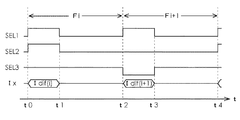
図4は、図3に示した画素回路の動作タイミングチャートである。上述した1Fに相当
する期間t0〜t2(またはt2〜t4)における一連の動作プロセスは、期間t0〜t1(ま
たはt2〜t3)のデータ書込プロセスと、これに続く期間t1〜t2(またはt3〜t4)の
駆動プロセスとに大別される。第1の走査信号SEL1によって、一方の駆動系20aの
動作状態が設定され、第2の走査信号SEL2によって、他方の駆動系20bの動作状態
が設定される。また、第3の走査信号SEL3によって、データ書込プロセスおよび駆動
プロセスのいずれかが指示される。なお、以下の説明では、同図に示した連続した複数の
フレームにおいて、i番目のフレームをFiとし、その後のフレームをFi+1、その前のフ
レームをFi-1とする。
FIG. 4 is an operation timing chart of the pixel circuit shown in FIG. A series of operation processes in the period t0 to t2 (or t2 to t4) corresponding to 1F described above are the data writing process in the period t0 to t1 (or t2 to t3) and the subsequent period t1 to t2 (or t3). To t4). The operation state of one
まず、フレームFiのデータ書込期間t0〜t1では、第1の走査信号SEL1がHレベル
であるから、一方の駆動系20aが動作状態になる。具体的には、タイミングt0におい
て、第1の走査信号SEL1がLレベルからHレベルに立ち上がる。これにより、トラン
ジスタT1がオンして、一方の駆動系20aの入力ノードN1と、データ線Xとが電気的に
接続される。正駆動部に関しては、トランジスタT2がオンして、pチャネル型のトラン
ジスタT3の一方の端子と自己のゲートとがダイオード接続される。ダイオード接続され
たトランジスタT3は、チャネル電流が流れることを前提に生じるゲート電圧に応じて、
キャパシタC1へのデータ書き込みを行うプログラミング素子として機能する。負駆動部
に関しても同様であり、トランジスタT4がオンして、nチャネル型のトランジスタT5の
一方の端子と自己のゲートとがダイオード接続される。ダイオード接続されたトランジス
タT5は、チャネル電流が流れることを前提に発生するゲート電圧に応じて、キャパシタ
C2へのデータ書き込みを行うプログラミング素子として機能する。なお、この期間t0〜
t1では、第2の走査信号SEL2がLレベルであるから、他方の駆動系20bは非動作状
態のままである。したがって、他方の駆動系20bのキャパシタC3,C4は、従前のフレ
ームFi-1で書き込まれた差分データIdif(i-1)を引き続き保持する。
First, in the data writing period t0 to t1 of the frame Fi, since the first scanning signal SEL1 is at the H level, one
It functions as a programming element for writing data to the capacitor C1. The same applies to the negative drive section. The transistor T4 is turned on, and one terminal of the n-channel transistor T5 and its own gate are diode-connected. The diode-connected transistor T5 functions as a programming element for writing data to the capacitor C2 in accordance with a gate voltage generated on the assumption that a channel current flows. This period t0 ~
At t1, since the second scanning signal SEL2 is at the L level, the
一方の駆動系20aのキャパシタC1,C2のどちらを主体にデータの書き込みが行われ
るかは、フレームFiにおける差分データIdif(i)の電流方向に依存している。図5(a
)に示すように、差分データIdif(i)の電流方向を、画素回路から可変電流源4aに向か
う方向に設定した場合(Idif(i)=Ipls1)、正駆動部におけるキャパシタC1のデータ
書き込みが行われる。すなわち、ダイオード接続されたトランジスタT3のゲートには、
自己のチャネルを流れる差分データIpls1の電流レベルに応じた電圧Vgが発生し、この
ゲート電圧Vgと電源電圧Vddとの電位差相当の電荷がキャパシタC1に蓄積される。この
場合、負駆動部におけるトランジスタT5のチャネル電流がほぼ0なので、キャパシタC2
の保持データは、トランジスタT5のしきい値電圧Vth相当にリセットされる。差分デー
タIdif(i)がIpls1となるのは、Di−ΔDi-1>0の場合であり、その電圧レベル(絶対
値)は、差分値の増加にともない大きくなる。
Which of the capacitors C1 and C2 of one
), When the current direction of the difference data Idif (i) is set in the direction from the pixel circuit to the variable
A voltage Vg corresponding to the current level of the differential data Ipls1 flowing through its own channel is generated, and a charge corresponding to the potential difference between the gate voltage Vg and the power supply voltage Vdd is accumulated in the capacitor C1. In this case, since the channel current of the transistor T5 in the negative drive section is almost zero, the capacitor C2
The held data is reset to the threshold voltage Vth of the transistor T5. The difference data Idif (i) becomes Ipls1 when Di−ΔDi−1> 0, and the voltage level (absolute value) increases as the difference value increases.
これに対して、図5(b)に示すように、差分データIdif(i)の電流方向を、可変電流
源4aから画素回路に向かう方向に設定した場合(Idif(i)=Imns1)、負駆動部におけ
るキャパシタC2のデータ書き込みが行われる。すなわち、ダイオード接続されたトラン
ジスタT5のゲートには、自己のチャネルを流れる差分データImns1の電流レベルに応じ
た電圧Vgが発生し、このゲート電圧Vgと電源電圧Vssとの電位差相当の電荷がキャパシ
タC2に蓄積される。この場合、正駆動部におけるトランジスタT3のチャネル電流がほぼ
0なので、キャパシタC1の保持データは、トランジスタT3のしきい値電圧Vth相当にリ
セットされる。差分データIdif(i)がImns1となるのは、(Di−ΔDi-1)<0の場合で
あり、その電圧レベル(絶対値)は、差分値の増加に伴い大きくなる。
On the other hand, as shown in FIG. 5B, when the current direction of the difference data Idif (i) is set to the direction from the variable
なお、データ書込期間t0〜t1では、第3の走査信号SEL3がLレベルなのでトラン
ジスタT6,T12がオフし、2つの駆動系20a,20bのノードN1,N2と、有機EL
素子OLEDのアノードとが電気的に分離される。したがって、この期間t0〜t1において、
有機EL素子OLEDは発光しない。この点は、次のフレームFi+1のデータ書込期間t2〜t
3においても同様である。
In the data writing period t0 to t1, since the third scanning signal SEL3 is at the L level, the transistors T6 and T12 are turned off, the nodes N1 and N2 of the two
The anode of the element OLED is electrically separated. Therefore, in this period t0 to t1,
The organic EL element OLED does not emit light. This is because the data writing period t2-t of the next frame Fi + 1
The same applies to 3.
続く駆動期間t1〜t2では、2つの駆動系20a,20bからの駆動電流Ioled1,Io
led2を合成した合成電流Ioledが有機EL素子OLEDに供給される。タイミングt1におい
て、第1の走査信号SEL1がHレベルからLレベルに立ち下がる。これにより、トラン
ジスタT1がオフして、一方の駆動系20aのノードN1とデータ線Xとが電気的に分離さ
れる。それとともに、トランジスタT2,T4もオフして、トランジスタT3,T5のダイオ
ード接続が解消される。しかしながら、キャパシタC1,C2には先に書き込まれたデータ
が保持されている。したがって、タイミングt1以降も、キャパシタC1,C2の保持デー
タに応じたゲート電圧VgがトランジスタT3,T5のゲートに印加され続ける。また、こ
のタイミングt1で、第3の走査信号SEL3がLレベルからHレベルに立ち上がる。これ
により、トランジスタT6がオンして、一方の駆動系20aの出力ノードN1と、有機EL
素子OLEDのアノードとが電気的に接続される。その結果、一方の駆動系20aから有機E
L素子OLEDを経てVss端子に向かう、駆動電流Ioled1の経路が形成される。この駆動電
流Ioled1は、トランジスタT3(またはT5)のチャネル電流に相当し、その電流レベル
は、自己のゲート電圧Vgに基づいて、換言すれば、このゲート電圧Vgを発生するキャパ
シタC1(またはC2)の保持データに基づいて一義的に特定される。また、タイミングt
1で、トランジスタT6と共にトランジスタT12もオンして、他方の駆動系20bの出力ノ
ードN2と、有機EL素子OLEDのアノードとが電気的に接続される。その結果、他方の駆
動系20bから有機EL素子OLEDを経てVss端子に向かう、駆動電流Ioled2の経路が形
成される。この駆動電流Ioled2は、トランジスタT9(またはT11)のチャネル電流に相
当し、その電流レベルは、自己のゲート電圧Vgに基づいて、換言すれば、このゲート電
圧Vgを発生するキャパシタC3(またはC4)の保持データに基づいて一義的に特定され
る。有機EL素子OLEDには、2つの駆動電流Ioled1,Ioled2を合成した合成電流Ioled
が流れ、これにより、有機EL素子OLEDの輝度が本来の階調データDi相当に設定される
。
In the subsequent drive period t1 to t2, the drive currents Ioled1, Io from the two
A combined current Ioled obtained by combining led2 is supplied to the organic EL element OLED. At timing t1, the first scanning signal SEL1 falls from the H level to the L level. Thereby, the transistor T1 is turned off, and the node N1 and the data line X of one
The anode of the element OLED is electrically connected. As a result, from one
A path of the drive current Ioled1 is formed that goes to the Vss terminal through the L element OLED. This drive current Ioled1 corresponds to the channel current of the transistor T3 (or T5), and its current level is based on its own gate voltage Vg, in other words, the capacitor C1 (or C2) that generates this gate voltage Vg. Are uniquely identified based on the stored data. In addition, timing t
1, the transistor T12 is turned on together with the transistor T6, and the output node N2 of the
Thus, the luminance of the organic EL element OLED is set to be equivalent to the original gradation data Di.
駆動電流Ioled1,Ioled2に基づく合成電流Ioled(≧0)の合成パターンには、以下
の3通りがある。なお、差分データΔDの特性上、合成電流Ioledが負となるケース、す
なわち、Ioled1=Imns2、Ioled2=Imns2のケースは存在しない。
There are the following three combinations of combined currents Ioled (≧ 0) based on the drive currents Ioled1 and Ioled2. Note that there is no case where the combined current Ioled is negative due to the characteristics of the difference data ΔD, that is, the case where Ioled1 = Imns2 and Ioled2 = Imns2.
(パターン1)Ioled1=Ipls1かつIoled2=Ipls2(図5(c))
フレームFiで一方の駆動系20aに供給された差分データIdif(i)がIpls1の場合に
は、トランジスタT3にチャネル電流が流れて、順駆動電流Ioled1(=Ipls1)が生成さ
れる。また、フレームFi-1で他方の駆動系20bに供給された差分データIdif(i-1)が
Ipls2の場合には、トランジスタT9にチャネル電流が流れて、順駆動電流Ioled2(=I
pls2)が生成される。この場合の合成電流Ioledは、2つの順駆動電流Ioled1,Ioled2
を加算したレベル(Ipls1+Ipls2)になる。駆動電流Ioled1,Ioled2の方向は、合成
電流Ioledの電流方向を基準に決定され、合成電流Ioledを増加させる方向を「順方向」
と定義し、合成電流Ioledを減少させる方向を「逆方向」と定義する。
(Pattern 1) Ioled1 = Ipls1 and Ioled2 = Ipls2 (FIG. 5C)
When the difference data Idif (i) supplied to one
pls2) is generated. In this case, the combined current Ioled is two forward drive currents Ioled1 and Ioled2.
Becomes the level (Ipls1 + Ipls2). The directions of the drive currents Ioled1 and Ioled2 are determined based on the current direction of the combined current Ioled, and the direction in which the combined current Ioled is increased is “forward”.
The direction in which the combined current Ioled is reduced is defined as “reverse direction”.
(パターン2)Ioled1=Ipls1かつIoled2=Imns2(図5(d))
フレームFiで一方の駆動系20aに供給された差分データIdif(i)がIpls1の場合に
は、トランジスタT3にチャネル電流が流れて、順駆動電流Ioled1(=Ipls1)が生成さ
れる。また、フレームFi-1で他方の駆動系20bに供給された差分データIdif(i-1)が
Imns2の場合には、トランジスタT11にチャネル電流が流れて、逆駆動電流Ioled2(=
Imns2)が生成される。この場合の合成電流Ioledは、順駆動電流Ioled1から、これと
は逆向きの逆方向電流Ioled2を減算したレベル(Ipls1−Imns2)になる。
(Pattern 2) Ioled1 = Ipls1 and Ioled2 = Imns2 (FIG. 5D)
When the difference data Idif (i) supplied to one
Imns2) is generated. The combined current Ioled in this case has a level (Ipls1-Imns2) obtained by subtracting the reverse current Ioled2 in the opposite direction from the forward drive current Ioled1.
(パターン3)Ioled1=Imns1かつIoled2=Ipls2
フレームFiで一方の駆動系20aに供給された差分データIdif(i)がImns1の場合に
は、トランジスタT5にチャネル電流が流れて、逆駆動電流Ioled1(=Imns1)が生成さ
れる。また、フレームFi-1で他方の駆動系20bに供給された差分データIdif(i-1)が
Ipls2の場合には、トランジスタT9にチャネル電流が流れて、順駆動電流Ioled2(=I
pls2)が生成される。この場合の合成電流Ioledは、順駆動電流Ioled2から、これとは
逆向きの逆方向電流Ioled1を減算したレベル(Ipls2−Imns1)になる。
(Pattern 3) Ioled1 = Imns1 and Ioled2 = Ipls2
When the difference data Idif (i) supplied to one
pls2) is generated. The combined current Ioled in this case has a level (Ipls2-Imns1) obtained by subtracting the reverse current Ioled1 in the opposite direction from the forward drive current Ioled2.
フレームFiに続くフレームFi+1におけるデータ書込期間t2〜t3では、第2の走査信
号SEL2がHレベルであるから、他方の駆動系20bが動作状態になる。これにより、
他方の駆動系20bの正駆動部に関しては、トランジスタT8がオンして、pチャネル型
のトランジスタT9の一方の端子と自己のゲートとがダイオード接続される。ダイオード
接続されたトランジスタT9は、チャネル電流が流れることを前提に生じるゲート電圧に
応じて、キャパシタC3へのデータ書き込みを行うプログラミング素子として機能する。
負駆動部に関しても同様であり、トランジスタT10がオンして、トランジスタT11の一方
の端子と自己のゲートとがダイオード接続される。ダイオード接続されたトランジスタT
11は、チャネル電流が流れることを前提に発生するゲート電圧に応じて、キャパシタC4
へのデータ書き込みを行うプログラミング素子として機能する。なお、この期間t2〜t3
では、第1の走査信号SEL1がLレベルであるから、一方の駆動系20aは非動作状態
である。したがって、一方の駆動系20aのキャパシタC1,C2は、従前のフレームFi
で書き込まれた差分データIdif(i)を引き続き保持する。
In the data writing period t2 to t3 in the frame Fi + 1 following the frame Fi, since the second scanning signal SEL2 is at the H level, the
Regarding the positive drive part of the
The same applies to the negative drive unit, and the transistor T10 is turned on, and one terminal of the transistor T11 and its own gate are diode-connected. Diode-connected transistor T
11 is a capacitor C4 according to the gate voltage generated on the assumption that the channel current flows.
It functions as a programming element for writing data into the memory. This period t2 to t3
Then, since the first scanning signal SEL1 is at the L level, one
The differential data Idif (i) written in (1) is continuously held.
他方の駆動系20bのキャパシタC3,C4のどちらを主体にデータの書き込みが行われ
るかは、フレームFi+1における差分データIdif(i+1)の電流方向に依存している。すな
わち、Idif(i+1)=Ipls2の場合、正駆動部のトランジスタT9によって、キャパシタC3
のデータ書き込みが行われる。この場合、キャパシタC4の保持データは、トランジスタ
T11のしきい値電圧Vth相当にリセットされる。差分データIdif(i+1)がIpls2となるの
は、Di+1−ΔDi>0の場合であり、その電圧レベル(絶対値)は、差分値の増加にとも
ない大きくなる。これに対して、Idif(i+1)=Imns2の場合、負駆動部のトランジスタT
11によって、キャパシタC4のデータ書き込みが行われる。この場合、キャパシタC3の保
持データは、トランジスタT9のしきい値電圧Vth相当にリセットされる。差分データId
if(i+1)がImns2となるのは、(Di+1−ΔDi)<0の場合であり、その電圧レベル(絶
対値)は、差分値の増加に伴い大きくなる。
Which of the capacitors C3 and C4 of the
Is written. In this case, the data held in the capacitor C4 is reset to be equivalent to the threshold voltage Vth of the transistor T11. The difference data Idif (i + 1) becomes Ipls2 when Di + 1−ΔDi> 0, and the voltage level (absolute value) increases as the difference value increases. On the other hand, when Idif (i + 1) = Imns2, the transistor T of the negative drive unit
11, data is written to the capacitor C4. In this case, the data held in the capacitor C3 is reset to be equivalent to the threshold voltage Vth of the transistor T9. Difference data Id
if (i + 1) becomes Imns2 when (Di + 1−ΔDi) <0, and the voltage level (absolute value) increases as the difference value increases.
続く駆動期間t3〜t4では、2つの駆動系20a,20bからの駆動電流Ioled1,Io
led2を合成した合成電流Ioledが有機EL素子OLEDに供給される。タイミングt3におい
て、第2の走査信号SEL2がHレベルからLレベルに立ち下がる。これにより、トラン
ジスタT7がオフして、他方の駆動系20bのノードN2とデータ線Xとが電気的に分離さ
れる。それとともに、トランジスタT8,T10もオフして、トランジスタT9,T11のダイ
オード接続が解消される。しかしながら、キャパシタC3,C4には先に書き込まれたデー
タが保持されている。したがって、タイミングt3以降も、キャパシタC3,C4の保持デ
ータに応じたゲート電圧VgがトランジスタT9,T11のゲートに印加され続ける。また、
このタイミングt3で、第3の走査信号SEL3がLレベルからHレベルに立ち上がる。こ
れにより、トランジスタT12がオンして、他方の駆動系20bの出力ノードN2と、有機
EL素子OLEDのアノードとが電気的に接続される。その結果、他方の駆動系20bから有
機EL素子OLEDを経てVss端子に向かう、駆動電流Ioled2の経路が形成される。この駆
動電流Ioled2は、トランジスタT9(またはT11)のチャネル電流に相当し、その電流レ
ベルは、自己のゲート電圧Vgに基づいて、換言すれば、このゲート電圧Vgを発生するキ
ャパシタC3(またはC4)の保持データに基づいて一義的に特定される。また、タイミン
グt3で、トランジスタT12と共にトランジスタT6もオンして、一方の駆動系20aの出
力ノードN1と、有機EL素子OLEDのアノードとが電気的に接続される。その結果、一方
の駆動系20aから有機EL素子OLEDを経てVss端子に向かう、駆動電流Ioled1の経路
が形成される。この駆動電流Ioled1は、トランジスタT3(またはT5)のチャネル電流
に相当し、その電流レベルは、自己のゲート電圧Vgに基づいて、換言すれば、このゲー
ト電圧Vgを発生するキャパシタC1(またはC2)の保持データに基づいて一義的に特定
される。有機EL素子OLEDには、2つの駆動電流Ioled1,Ioled2を合成した合成電流I
oledが流れ、これにより、有機EL素子OLEDの輝度が本来の階調データDi+1相当に設定
される。
In the subsequent drive period t3 to t4, the drive currents Ioled1, Io from the two
A combined current Ioled obtained by combining led2 is supplied to the organic EL element OLED. At timing t3, the second scanning signal SEL2 falls from the H level to the L level. Thereby, the transistor T7 is turned off, and the node N2 and the data line X of the
At this timing t3, the third scanning signal SEL3 rises from the L level to the H level. Thereby, the transistor T12 is turned on, and the output node N2 of the
As a result, the luminance of the organic EL element OLED is set to be equivalent to the original gradation data Di + 1.
このように、本実施形態によれば、電流プログラム方式の画素回路において、互いに異
なる差分データIdif(i),Idif(i+1)を用いた差分駆動を行うことで、低消費電力化を図
ることが可能になる。なぜなら、微少電流での書き込みが問題にならないケース(例えば
、小型パネルで容量が小さく書込時間も長い場合、高輝度で発光するデバイス、高階調領
域の駆動等)において、データ線Xに大電流を供給する必要がなくなるからである。これ
に起因して、データ線駆動回路4内の電流DACにおける消費電力の低減を図ることがで
き、かつ、その回路構成を簡素化することができる。また、電流DACと画素回路との間
に存在するデータ線Xにおけるノイズの低減を図ることも可能になる。さらに、大規模な
ディスプレイの場合には、階調データがそのまま出力されることが多いので、中間回路に
負荷がかかるが、本実施形態の場合には、階調データを圧縮して扱うことができるので、
そのような負荷を低減できるという効果もある。
As described above, according to the present embodiment, in the current-programmed pixel circuit, the differential driving using the different difference data Idif (i) and Idif (i + 1) is performed to reduce the power consumption. It becomes possible. This is because in a case where writing with a small current is not a problem (for example, a small panel having a small capacity and a long writing time, a device that emits light with high brightness, driving in a high gradation region, etc.), a large current is applied to the data line X. This is because it is no longer necessary to supply. As a result, the power consumption of the current DAC in the data
There is also an effect that such a load can be reduced.
なお、上述した実施形態では、すべての階調領域で差分駆動を行っているが、階調領域
に応じて、差分データΔDを用いた差分駆動と、階調データDを用いた通常駆動とを切り
替えてもよい。例えば、表示部1の輝度が全体的に高い場合には差分駆動を行い、全体的
に低い場合には通常駆動を行うといった如くである。これにより、電流プログラム方式固
有の問題である、低階調時におけるデータ書き込み不足の抑制を図ることが可能になる。
また、表示対象に応じて、差分駆動と通常駆動とを切り替えてもよい。例えば、表示部1
に動画を表示する場合には差分駆動を行い、静止画を表示する場合には通常駆動を行うと
いった如くである。これにより、静止画の表示時における不要な書き込み(走査信号SE
L2の走査では何も書き込まれない)を解消できる。なお、通常駆動時には、図3に示し
た走査信号SEL2を走査せずに、走査信号SEL1,SEL3を走査することで、一方の
駆動系20aのみを用いた駆動を行えばよい。以上の点は、後述する各実施形態において
も同様である。
In the above-described embodiment, the differential drive is performed in all the gradation regions. However, the differential drive using the difference data ΔD and the normal drive using the gradation data D are performed according to the gradation region. You may switch. For example, differential driving is performed when the luminance of the
Further, the differential drive and the normal drive may be switched according to the display target. For example,
When a moving image is displayed, differential driving is performed, and when a still image is displayed, normal driving is performed. As a result, unnecessary writing (scanning signal SE when displaying a still image) is performed.
Nothing is written in the L2 scan). Note that during normal driving, driving using only one
(第2の実施形態)
図6は、本実施形態にかかる電流プログラム方式の画素回路図である。図1に示した1
本の走査線Yは、図示した3本の走査線Ya〜Ycのセットに相当する。この画素回路は、
有機EL素子OLEDと、14個のトランジスタT1〜T14と、4個のキャパシタC1〜C4と
で構成されている。本実施形態にかかる画素回路も、交互に動作する2つの駆動系20a
,2bを備えており、一方の駆動系20aが8つの回路要素T2〜T7,C1〜C2、他方の
駆動系20bが8つの回路要素T8〜T13,C3〜C4でそれぞれ構成されている。なお、
同図の例では、トランジスタT4,T8〜T12,T14をpチャネル型とし、その他をnチャ
ネル型としているが、これは一例にすぎず、別の組み合わせでチャネル型を設定してもよ
い。
(Second Embodiment)
FIG. 6 is a pixel circuit diagram of a current programming method according to the present embodiment. 1 shown in FIG.
The scanning line Y corresponds to a set of the three scanning lines Ya to Yc shown in the figure. This pixel circuit
It is composed of an organic EL element OLED, 14 transistors T1 to T14, and 4 capacitors C1 to C4. The pixel circuit according to this embodiment also includes two
2b, one
In the example of the figure, the transistors T4, T8 to T12, and T14 are p-channel type, and the others are n-channel type, but this is only an example, and the channel type may be set in another combination.
スイッチング素子であるトランジスタT1のゲートは、第1の走査信号SEL1が供給さ
れる第1の走査線Yaに接続されており、その一方の端子は、電流レベルの差分データId
ifが供給されるデータ線Xに接続されている。このトランジスタT1の他方の端子は、一
方の駆動系20aの入出力ノードであり、かつ、他方の駆動系20bの入出力ノードでも
あるノードN1に接続されている。また、スイッチング素子であるトランジスタT14のゲ
ートは、第1の走査線Yaに接続されており、その一方の端子は、ノードN1に接続されて
いる。このトランジスタT14の他方の端子は、有機EL素子OLEDのアノードに接続されて
いる。有機EL素子OLEDのカソードは、Vss端子に接続されている。
The gate of the transistor T1, which is a switching element, is connected to the first scanning line Ya to which the first scanning signal SEL1 is supplied, and one terminal thereof is the current level difference data Id.
It is connected to the data line X to which if is supplied. The other terminal of the transistor T1 is connected to a node N1 which is an input / output node of one
一方の駆動系20aは、4つの回路要素T2〜T4,C1によって構成される正駆動部と
、4つの回路要素T5〜T7,C2によって構成される負駆動部とを有する。正駆動部に関
して、スイッチング素子であるトランジスタT2のゲートは、第2の走査線Ybに接続され
ており、その一方の端子は、ノードN1に接続されている。また、トランジスタT2の他方
の端子は、駆動素子であるpチャネル型のトランジスタT4のゲートと、キャパシタC1の
一方の電極とに共通接続されている。このキャパシタC1の他方の電極は、トランジスタ
T4の一方の端子と共にVdd端子に接続され、トランジスタT4の他方の端子は、スイッチ
ング素子であるトランジスタT3の一方の端子に接続されている。このトランジスタT3の
ゲートは、第3の走査信号SEL3が供給される第3の走査線Ycに接続されており、その
他方の端子はノードN1に接続されている。一方、負駆動部に関して、スイッチング素子
であるトランジスタT5のゲートは、トランジスタT2と同様に第2の走査線Ybに接続さ
れており、その一方の端子は、ノードN1に接続されている。また、トランジスタT5の他
方の端子は、駆動素子であるnチャネル型のトランジスタT7のゲートと、キャパシタC2
の一方の電極とに共通接続されている。このキャパシタC2の他方の電極は、トランジス
タT7の一方の端子と共にVss端子に接続され、トランジスタT7の他方の端子は、スイッ
チング素子であるトランジスタT6の一方の端子に接続されている。このトランジスタT6
のゲートは、トランジスタT3と同様に第3の走査線Ycに接続されており、その他方の端
子はノードN1に接続されている。
One
Are commonly connected to one of the electrodes. The other electrode of the capacitor C2 is connected to the Vss terminal together with one terminal of the transistor T7, and the other terminal of the transistor T7 is connected to one terminal of the transistor T6 which is a switching element. This transistor T6
Is connected to the third scanning line Yc in the same manner as the transistor T3, and the other terminal is connected to the node N1.
また、他方の駆動系20bは、4つの回路要素T8〜T10,C3によって構成される正駆
動部と、4つの回路要素T11〜T13,C4によって構成される負駆動部とを有する。正駆
動部に関して、スイッチング素子であるトランジスタT8のゲートは、第3の走査線Ycに
接続されており、その一方の端子は、ノードN1に接続されている。また、トランジスタ
T8の他方の端子は、駆動素子であるpチャネル型のトランジスタT10のゲートと、キャ
パシタC3の一方の電極とに共通接続されている。このキャパシタC3の他方の電極は、ト
ランジスタT10の一方の端子と共にVdd端子に接続され、トランジスタT10の他方の端子
は、スイッチング素子であるトランジスタT9の一方の端子に接続されている。このトラ
ンジスタT9のゲートは、第2の走査線Ybに接続されており、その他方の端子はノードN
1に接続されている。一方、負駆動部に関して、スイッチング素子であるトランジスタT1
1のゲートは、トランジスタT8と同様に第3の走査線Ycに接続されており、その一方の
端子は、ノードN1に接続されている。また、トランジスタT11の他方の端子は、駆動素
子であるnチャネル型のトランジスタT13のゲートと、キャパシタC4の一方の電極とに
共通接続されている。このキャパシタC4の他方の電極は、トランジスタT13の一方の端
子と共にVss端子に接続され、トランジスタT13の他方の端子は、スイッチング素子であ
るトランジスタT12の一方の端子に接続されている。このトランジスタT12のゲートは、
トランジスタT9と同様に第2の走査線Ybに接続されており、その他方の端子はノードN
1に接続されている。
The
Connected to one. On the other hand, with respect to the negative drive unit, the transistor T1 which is a switching element
Similarly to the transistor T8, the gate of 1 is connected to the third scanning line Yc, and one terminal thereof is connected to the node N1. The other terminal of the transistor T11 is commonly connected to the gate of an n-channel transistor T13, which is a driving element, and to one electrode of the capacitor C4. The other electrode of the capacitor C4 is connected to the Vss terminal together with one terminal of the transistor T13, and the other terminal of the transistor T13 is connected to one terminal of the transistor T12 which is a switching element. The gate of this transistor T12 is
Similar to the transistor T9, it is connected to the second scanning line Yb, and the other terminal is connected to the node N.
Connected to one.
図7は、図6に示した画素回路の動作タイミングチャートである。上述した1Fに相当
する期間t0〜t2(またはt2〜t4)における一連の動作プロセスは、期間t0〜t1(ま
たはt2〜t3)のデータ書込プロセスと、これに続く期間t1〜t2(またはt3〜t4)の
駆動プロセスとに大別される。第1の走査信号SEL1によって、データ書込プロセスお
よび駆動プロセスのいずれかが指示される。また、第2および第3の走査信号SEL2,
SEL3によって、駆動系20a,20bの動作状態が設定される。
FIG. 7 is an operation timing chart of the pixel circuit shown in FIG. A series of operation processes in the period t0 to t2 (or t2 to t4) corresponding to 1F described above are the data writing process in the period t0 to t1 (or t2 to t3) and the subsequent period t1 to t2 (or t3). To t4). Either the data writing process or the driving process is instructed by the first scanning signal SEL1. The second and third scanning signals SEL2,
The operating state of the
まず、フレームFiのデータ書込期間t0〜t1では、第1の走査信号SEL1がHレベル
であるから、トランジスタT1がオンして、ノードN1とデータ線Xとが電気的に接続され
る。また、第2および第3の走査信号SEL2,SEL3が共にHレベルであるから、トラ
ンジスタT2,T3,T5,T6が共にオンし、一方の駆動系20aが動作状態になる。これ
により、正駆動部におけるpチャネル型のトランジスタT4の一方の端子と自己のゲート
とがダイオード接続される。ダイオード接続されたトランジスタT4は、チャネル電流が
流れることを前提に生じるゲート電圧に応じて、キャパシタC1へのデータ書き込みを行
うプログラミング素子として機能する。負駆動部に関しても同様であり、nチャネル型の
トランジスタT7の一方の端子と自己のゲートとがダイオード接続される。ダイオード接
続されたトランジスタT7は、チャネル電流が流れることを前提に発生するゲート電圧に
応じて、キャパシタC2へのデータ書き込みを行うプログラミング素子として機能する。
一方の駆動系20aのキャパシタC1,C2のどちらを主体にデータの書き込みが行われる
かは、上述した第1の実施形態と同様、フレームFiにおける差分データIdif(i)の電流
方向に依存している。なお、この期間t0〜t1では、第2および第3の走査信号SEL2
,SEL3によって導通制御されるトランジスタT8,T9,T11,T12が共にオフである
から、他方の駆動系20bは非動作状態のままである。したがって、他方の駆動系20b
のキャパシタC3,C4は、従前のフレームFi-1で書き込まれた差分データIdif(i-1)を
引き続き保持する。
First, in the data write period t0 to t1 of the frame Fi, since the first scanning signal SEL1 is at the H level, the transistor T1 is turned on and the node N1 and the data line X are electrically connected. Further, since the second and third scanning signals SEL2 and SEL3 are both at the H level, the transistors T2, T3, T5 and T6 are all turned on, and one
Which of the capacitors C1 and C2 of one
, SEL3, the transistors T8, T9, T11, and T12, all of which are turned off, are off, and the
The capacitors C3 and C4 continue to hold the differential data Idif (i-1) written in the previous frame Fi-1.
なお、データ書込期間t0〜t1では、第1の走査信号SEL1がHレベルなのでトラン
ジスタT14がオフし、ノードN1と有機EL素子OLEDのアノードとが電気的に分離される
。したがって、この期間t0〜t1において、有機EL素子OLEDは発光しない。この点は、
次のフレームFi+1のデータ書込期間t2〜t3においても同様である。
In the data writing period t0 to t1, since the first scanning signal SEL1 is at the H level, the transistor T14 is turned off, and the node N1 and the anode of the organic EL element OLED are electrically separated. Therefore, the organic EL element OLED does not emit light during this period t0 to t1. This point
The same applies to the data writing periods t2 to t3 of the next frame Fi + 1.
続く駆動期間t1〜t2では、2つの駆動系20a,20bからの駆動電流Ioled1,Io
led2を合成した合成電流Ioledが有機EL素子OLEDに供給される。タイミングt1におい
て、第1の走査信号SEL1がHレベルからLレベルに立ち下がる。これにより、トラン
ジスタT1がオフして、ノードN1とデータ線Xとが電気的に分離される。それとともに、
トランジスタT14がオンして、ノードN1と有機EL素子OLEDのアノードとが電気的に接
続される。また、タイミングt1で、第2の走査信号SEL2もHレベルからLレベルに立
ち下がる。これにより、一方の駆動系20aに関して、トランジスタT2,T5がオフして
、トランジスタT4,T7のダイオード接続が解消される。しかしながら、キャパシタC1
,C2には先に書き込まれたデータが保持されている。したがって、タイミングt1以降も
、キャパシタC1,C2の保持データに応じたゲート電圧VgがトランジスタT4,T7のゲ
ートに印加され続ける。その結果、一方の駆動系20aから有機EL素子OLEDを経てVss
端子に向かう、駆動電流Ioled1の経路が形成される。この駆動電流Ioled1は、トランジ
スタT4(またはT7)のチャネル電流に相当し、その電流レベルは、自己のゲート電圧V
gに基づいて、換言すれば、このゲート電圧Vgを発生するキャパシタC1(またはC2)の
保持データに基づいて一義的に特定される。また、第2の走査信号SEL2がLレベルに
立ち下がったことで、他方の駆動系20bのトランジスタT9,T12が共にオンする。そ
の結果、他方の駆動系20bから有機EL素子OLEDを経てVss端子に向かう、駆動電流I
oled2の経路が形成される。この駆動電流Ioled2は、トランジスタT10(またはT13)の
チャネル電流に相当し、その電流レベルは、自己のゲート電圧Vgに基づいて、換言すれ
ば、このゲート電圧Vgを発生するキャパシタC3(またはC4)の保持データに基づいて
一義的に特定される。有機EL素子OLEDには、2つの駆動電流Ioled1,Ioled2を合成し
た合成電流Ioledが流れ、これにより、有機EL素子OLEDの輝度が本来の階調データDi
相当に設定される。駆動電流Ioled1,Ioled2に基づく合成電流Ioled(≧0)の合成パ
ターンについては、上述した第1の実施形態と同様であるから、ここでの説明を省略する
。
In the subsequent drive period t1 to t2, the drive currents Ioled1, Io from the two
A combined current Ioled obtained by combining led2 is supplied to the organic EL element OLED. At timing t1, the first scanning signal SEL1 falls from the H level to the L level. Thereby, the transistor T1 is turned off, and the node N1 and the data line X are electrically separated. With that,
The transistor T14 is turned on, and the node N1 and the anode of the organic EL element OLED are electrically connected. Further, at the timing t1, the second scanning signal SEL2 also falls from the H level to the L level. Thereby, with respect to one
, C2 holds previously written data. Accordingly, the gate voltage Vg corresponding to the data held in the capacitors C1 and C2 is continuously applied to the gates of the transistors T4 and T7 even after the timing t1. As a result, Vss from one
A path of the drive current Ioled1 toward the terminal is formed. This drive current Ioled1 corresponds to the channel current of the transistor T4 (or T7), and its current level is determined by its own gate voltage V
In other words, it is uniquely specified based on data held in the capacitor C1 (or C2) that generates the gate voltage Vg. Further, since the second scanning signal SEL2 falls to the L level, the transistors T9 and T12 of the
The pathway of oled2 is formed. This drive current Ioled2 corresponds to the channel current of the transistor T10 (or T13), and its current level is based on its own gate voltage Vg, in other words, the capacitor C3 (or C4) that generates this gate voltage Vg. Are uniquely identified based on the stored data. In the organic EL element OLED, a combined current Ioled obtained by synthesizing two driving currents Ioled1 and Ioled2 flows, and thereby the luminance of the organic EL element OLED is the original gradation data Di.
It is set considerably. Since the combined pattern of the combined current Ioled (≧ 0) based on the drive currents Ioled1 and Ioled2 is the same as that in the first embodiment described above, description thereof is omitted here.
次のフレームFi+1のデータ書込期間t2〜t3では、第1の走査信号SEL1がHレベル
であるから、トランジスタT1がオンして、ノードN1とデータ線Xとが電気的に接続され
る。また、第2および第3の走査信号SEL2,SEL3が共にLレベルであるから、トラ
ンジスタT8,T9,T11,T12が共にオンし、他方の駆動系20bが動作状態になる。こ
れにより、正駆動部におけるpチャネル型のトランジスタT10の一方の端子と自己のゲー
トとがダイオード接続される。ダイオード接続されたトランジスタT10は、チャネル電流
が流れることを前提に生じるゲート電圧に応じて、キャパシタC3へのデータ書き込みを
行うプログラミング素子として機能する。負駆動部に関しても同様であり、nチャネル型
のトランジスタT13の一方の端子と自己のゲートとがダイオード接続される。ダイオード
接続されたトランジスタT13は、チャネル電流が流れることを前提に発生するゲート電圧
に応じて、キャパシタC4へのデータ書き込みを行うプログラミング素子として機能する
。他方の駆動系20bのキャパシタC3,C4のどちらを主体にデータの書き込みが行われ
るかは、フレームFi+1における差分データIdif(i+1)の電流方向に依存している。なお
、この期間t2〜t3では、第2および第3の走査信号SEL2,SEL3によって導通制御
されるトランジスタT2,T3,T5,T6が共にオフであるから、一方の駆動系20aは非
動作状態のままである。したがって、一方の駆動系20aのキャパシタC1,C2は、従前
のフレームFiで書き込まれた差分データIdif(i)を引き続き保持する。
In the data writing period t2 to t3 of the next frame Fi + 1, since the first scanning signal SEL1 is at the H level, the transistor T1 is turned on and the node N1 and the data line X are electrically connected. . Since the second and third scanning signals SEL2 and SEL3 are both at the L level, the transistors T8, T9, T11, and T12 are all turned on, and the
続く駆動期間t3〜t4では、2つの駆動系20a,20bからの駆動電流Ioled1,Io
led2を合成した合成電流Ioledが有機EL素子OLEDに供給される。タイミングt3におい
て、第1の走査信号SEL1がHレベルからLレベルに立ち下がる。これにより、トラン
ジスタT1がオフして、ノードN1とデータ線Xとが電気的に分離されるとともに、トラン
ジスタT14がオンして、ノードN1と有機EL素子OLEDのアノードとが電気的に接続され
る。また、タイミングt3で、第3の走査信号SEL3がLレベルからHレベルに立ち上が
る。これにより、他方の駆動系20bに関して、トランジスタT8,T11がオフして、ト
ランジスタT10,T13のダイオード接続が解消される。しかしながら、キャパシタC3,
C4には先に書き込まれたデータが保持されているので、タイミングt3以降も、これらの
保持データに応じたゲート電圧VgがトランジスタT10,T13のゲートに印加され続ける
。また、この期間t3〜t4では、第2の走査信号SEL2がLレベルのままなので、トラ
ンジスタT9,T12は引き続きオンする。その結果、他方の駆動系20bから有機EL素
子OLEDを経てVss端子に向かう、駆動電流Ioled2の経路が形成される。この駆動電流Io
led2は、トランジスタT10(またはT13)のチャネル電流に相当し、その電流レベルは、
自己のゲート電圧Vgに基づいて、換言すれば、このゲート電圧Vgを発生するキャパシタ
C3(またはC4)の保持データに基づいて一義的に特定される。また、第3の走査信号S
EL3がHレベルに立ち上がることによって、一方の駆動系20aのトランジスタT3,T
6が共にオンする。その結果、一方の駆動系20aから有機EL素子OLEDを経てVss端子
に向かう、駆動電流Ioled1の経路が形成される。この駆動電流Ioled1は、トランジスタ
T4(またはT7)のチャネル電流に相当し、その電流レベルは、自己のゲート電圧Vgに
基づいて、換言すれば、このゲート電圧Vgを発生するキャパシタC1(またはC2)の保
持データに基づいて一義的に特定される。有機EL素子OLEDには、2つの駆動電流Ioled
1,Ioled2を合成した合成電流Ioledが流れ、これにより、有機EL素子OLEDの輝度が本
来の階調データDi+1相当に設定される。
In the subsequent drive period t3 to t4, the drive currents Ioled1, Io from the two
A combined current Ioled obtained by combining led2 is supplied to the organic EL element OLED. At timing t3, the first scanning signal SEL1 falls from H level to L level. As a result, the transistor T1 is turned off to electrically isolate the node N1 and the data line X, and the transistor T14 is turned on to electrically connect the node N1 and the anode of the organic EL element OLED. . At the timing t3, the third scanning signal SEL3 rises from the L level to the H level. Thereby, with respect to the
Since the previously written data is held in C4, the gate voltage Vg corresponding to the held data is continuously applied to the gates of the transistors T10 and T13 after the timing t3. In this period t3 to t4, since the second scanning signal SEL2 remains at the L level, the transistors T9 and T12 are continuously turned on. As a result, a path of the drive current Ioled2 is formed from the
led2 corresponds to the channel current of transistor T10 (or T13) and its current level is
Based on its own gate voltage Vg, in other words, it is uniquely specified based on data held in the capacitor C3 (or C4) that generates the gate voltage Vg. The third scanning signal S
As EL3 rises to the H level, transistors T3, T of one
6 turns on together. As a result, a path of the drive current Ioled1 is formed from one
A combined current Ioled that combines 1 and Ioled2 flows, whereby the luminance of the organic EL element OLED is set to be equivalent to the original gradation data Di + 1.
このように、本実施形態によれば、電流プログラム方式の画素回路において、互いに異
なる差分データIdif(i),Idif(i+1)を用いた差分駆動を行うことで、低消費電力化を含
む第1の実施形態と同様の効果が得られる。
As described above, according to the present embodiment, in the current-programmed pixel circuit, differential driving using different differential data Idif (i) and Idif (i + 1) is performed, thereby reducing power consumption. The same effect as in the first embodiment can be obtained.
(第3の実施形態)
上述した第1および第2の実施形態では、電流プログラム方式の差分駆動について説明
したが、第3および第4の実施形態では、電圧プログラム方式への適用例について説明す
る。本実施形態において、図1に示したデータ線駆動回路4は、電流DACの代わりに電
圧DACを含み、電圧レベルの差分データVdifをデータ線X〜Xmに供給する。本実施形
態では、隣接したフレーム間における「差分データΔD」の正負に基づいて差分データV
difを決定する。すなわち、Di+1−ΔDi>0の場合には、差分データVdifとして正の値
Vplsが設定され、これが第1のデータ線Xaに出力される。これに対して、(Di+1−Δ
Di)<0の場合には、差分データVdifとして負の値Vmnsが設定され、これが第2のデ
ータ線Xbに出力される。また、図1に示した1本の走査線Yは、図示した2本の走査線
Ya,Ybのセットに相当し、図1に示した1本のデータ線Xは、図示した2本のデータ線
Xa,Xbのセットに相当する。
(Third embodiment)
In the first and second embodiments described above, the differential driving of the current programming method has been described. In the third and fourth embodiments, application examples to the voltage programming method will be described. In the present embodiment, the data
Determine dif. That is, when Di + 1−ΔDi> 0, a positive value Vpls is set as the difference data Vdif, and this is output to the first data line Xa. On the other hand, (Di + 1−Δ
In the case of Di) <0, a negative value Vmns is set as the difference data Vdif, and this is output to the second data line Xb. Further, one scanning line Y shown in FIG. 1 corresponds to the set of two scanning lines Ya and Yb shown in the figure, and one data line X shown in FIG. 1 shows two data shown in the figure. It corresponds to a set of lines Xa and Xb.
図8は、本実施形態にかかる電圧プログラム方式の画素回路図である。この画素回路は
、有機EL素子OLEDと、8個のトランジスタT1〜T8と、4個のキャパシタC1〜C4とで
構成されている。本実施形態にかかる画素回路も、交互に動作する2つの駆動系20a,
2bを備えており、一方の駆動系20aが6つの回路要素T1〜T4,C1〜C2、他方の駆
動系20bが6つの回路要素T5〜T8,C3〜C4でそれぞれ構成されている。なお、同図
の例では、トランジスタT2,T6をpチャネル型とし、その他をnチャネル型としている
が、これは一例にすぎず、別の組み合わせでチャネル型を設定してもよい。
FIG. 8 is a pixel circuit diagram of a voltage program method according to the present embodiment. This pixel circuit is composed of an organic EL element OLED, eight transistors T1 to T8, and four capacitors C1 to C4. The pixel circuit according to the present embodiment also includes two
2b, one
一方の駆動系20aは、3つの回路要素T1,T2,C1によって構成される正駆動部と
、3つの回路要素T3,T4,C2によって構成される負駆動部とを有する。正駆動部に関
して、スイッチング素子であるトランジスタT1のゲートは、第1の走査信号SEL1が供
給される第1の走査線Yaに接続されている。このトランジスタT1の一方の端子は、電圧
レベルの差分データVdif(=Vpls)が供給される第1のデータ線Xaに接続されており
、その他方の端子は、キャパシタC1の一方の電極と、駆動素子であるpチャネル型のト
ランジスタT2のゲートとに共通接続されている。キャパシタC1の他方の電極は、トラン
ジスタT2の一方の端子と共にVdd端子に接続されており、トランジスタT2の他方の端子
は、ノードN1に接続されている。一方、負駆動部に関して、スイッチング素子であるト
ランジスタT3のゲートは、トランジスタT1と同様に第1の走査線Yaに接続されている
。このトランジスタT3の一方の端子は、電圧レベルの差分データVdif(=Vmns)が供
給される第2のデータ線Xbに接続されており、その他方の端子は、キャパシタC2の一方
の電極と、駆動素子であるnチャネル型のトランジスタT4のゲートとに共通接続されて
いる。キャパシタC2の他方の電極は、トランジスタT4の一方の端子と共にVss端子に接
続されており、トランジスタT4の他方の端子は、ノードN1に接続されている。有機EL
素子OLEDのアノードは、ノードN1に接続されており、そのカソードはVss端子に接続さ
れている。
One
The anode of the element OLED is connected to the node N1, and its cathode is connected to the Vss terminal.
他方の駆動系20bは、3つの回路要素T5,T6,C3によって構成される正駆動部と
、3つの回路要素T7,T8,C4によって構成される負駆動部とを有する。正駆動部に関
して、スイッチング素子であるトランジスタT5のゲートは、第2の走査信号SEL2が供
給される第2の走査線Ybに接続されている。このトランジスタT5の一方の端子は、第1
のデータ線Xaに接続されており、その他方の端子は、キャパシタC3の一方の電極と、駆
動素子であるpチャネル型のトランジスタT6のゲートとに共通接続されている。キャパ
シタC3の他方の電極は、トランジスタT6の一方の端子と共にVdd端子に接続されており
、トランジスタT6の他方の端子は、ノードN1に接続されている。一方、負駆動部に関し
て、スイッチング素子であるトランジスタT7のゲートは、トランジスタT5と同様に第2
の走査線Ybに接続されている。このトランジスタT7の一方の端子は、第2のデータ線X
bに接続されており、その他方の端子は、キャパシタC4の一方の電極と、駆動素子である
nチャネル型のトランジスタT8のゲートとに共通接続されている。キャパシタC4の他方
の電極は、トランジスタT8の一方の端子と共にVss端子に接続されており、トランジス
タT8の他方の端子は、ノードN1に接続されている。
The
The other terminal is commonly connected to one electrode of the capacitor C3 and the gate of a p-channel transistor T6 which is a driving element. The other electrode of the capacitor C3 is connected to the Vdd terminal together with one terminal of the transistor T6, and the other terminal of the transistor T6 is connected to the node N1. On the other hand, regarding the negative drive unit, the gate of the transistor T7 which is a switching element is the same as that of the transistor T5.
Are connected to the scanning line Yb. One terminal of the transistor T7 is connected to the second data line X
The other terminal is connected in common to one electrode of the capacitor C4 and the gate of an n-channel transistor T8 that is a driving element. The other electrode of the capacitor C4 is connected to the Vss terminal together with one terminal of the transistor T8, and the other terminal of the transistor T8 is connected to the node N1.
図9は、図8に示した画素回路の動作タイミングチャートである。1Fに相当する期間
t0〜t2(またはt2〜t4)における一連の動作プロセスは、期間t0〜t1(またはt2
〜t3)のデータ書込プロセスと、これに続く期間t1〜t2(またはt3〜t4)の駆動プ
ロセスとに大別される。
FIG. 9 is an operation timing chart of the pixel circuit shown in FIG. A series of operation processes in the period t0 to t2 (or t2 to t4) corresponding to 1F is performed in the period t0 to t1 (or t2).
To t3) and a driving process in the following period t1 to t2 (or t3 to t4).
まず、フレームFiのデータ書込期間t0〜t1では、一方の駆動系20aのキャパシタ
C1,C2に対するデータの書き込みが行われる。具体的には、タイミングt0において、
第1の走査信号SEL1がLレベルからHレベルに立ち上がり、トランジスタT1,T3が
共にオンする。第1のデータ線Xaより供給された差分データVdif(i)(=Vpls(i))は
、トランジスタT1を介して、キャパシタC1の一方の電極に供給される。これにより、キ
ャパシタC1に対するデータの書き込みが行われ、Vpls(i)に応じた電荷がキャパシタC1
に蓄積される。一方、第2のデータ線Xbより供給された差分データVdif(i)(=Vmns(i
))は、トランジスタT2を介して、キャパシタC2の一方の電極に供給される。これによ
り、キャパシタC2に対するデータの書き込みが行われ、Vmns(i)に応じた電荷がキャパ
シタC2に蓄積される。なお、この期間t0〜t1では、第2の走査信号SEL2がLレベル
であるから、他方の駆動系20bは非動作状態のままである。したがって、他方の駆動系
20bのキャパシタC3,C4は、従前のフレームFi-1におけるVdif(i-1)(=Vpls(i-1
),Vmns(i-1))を引き続き保持する。
First, in the data write period t0 to t1 of the frame Fi, data is written to the capacitors C1 and C2 of one
The first scanning signal SEL1 rises from the L level to the H level, and both the transistors T1 and T3 are turned on. The difference data Vdif (i) (= Vpls (i)) supplied from the first data line Xa is supplied to one electrode of the capacitor C1 through the transistor T1. As a result, data is written to the capacitor C1, and the charge corresponding to Vpls (i) is transferred to the capacitor C1.
Accumulated in. On the other hand, the difference data Vdif (i) (= Vmns (i) supplied from the second data line Xb.
)) Is supplied to one electrode of the capacitor C2 via the transistor T2. As a result, data is written to the capacitor C2, and charges corresponding to Vmns (i) are accumulated in the capacitor C2. In this period t0 to t1, since the second scanning signal SEL2 is at the L level, the
), Vmns (i-1)).
続く駆動期間t1〜t2では、2つの駆動系20a,20bからの駆動電流を合成した合
成電流Ioledが有機EL素子OLEDに供給される。タイミングt1において、第1の走査信
号SEL1がHレベルからLレベルに立ち下がる。これにより、一方の駆動系20aのト
ランジスタT1,T3が共にオフするとともに、データ線Xa,Xbに対する差分データVdi
f(i)の供給も停止する。しかしながら、トランジスタT2のゲートには、キャパシタC1の
保持データによって電圧Vpls(i)が引き続き印加されているので、これに応じた順駆動電
流Ipls1がトランジスタT2のチャネルを流れる。同様に、トランジスタT4のゲートには
、キャパシタC2の保持データによって電圧Vmns(i)が引き続き印加されているので、こ
れに応じた逆駆動電流Imns1がトランジスタT2のチャネルを流れる。したがって、一方
の駆動系20aから出力される駆動電流は、(Ipls1−Imns1)になる。また、他方の駆
動系20bに関して、トランジスタT6のゲートには、キャパシタC3の保持データによっ
て電圧Vpls(i-1)が印加されているので、これに応じた順駆動電流Ipls2がトランジスタ
T6のチャネルを流れる。同様に、トランジスタT8のゲートには、キャパシタC4の保持
データによって電圧Vmns(i-1)が印加されているので、これに応じた逆駆動電流Imns2が
トランジスタT8のチャネルを流れる。したがって、他方の駆動系20bから出力される
駆動電流は、(Ipls2−Imns2)になる。最終的な合成電流Ioledは((Ipls1−Imns1
)+(pls2−Imns2))になり、有機EL素子OLEDは、自己を流れる合成電流Ioledに応
じた輝度に設定される。
In the subsequent drive period t1 to t2, a combined current Ioled obtained by combining drive currents from the two
The supply of f (i) is also stopped. However, since the voltage Vpls (i) is continuously applied to the gate of the transistor T2 according to the data held in the capacitor C1, the forward drive current Ipls1 corresponding thereto flows through the channel of the transistor T2. Similarly, since the voltage Vmns (i) is continuously applied to the gate of the transistor T4 according to the data held in the capacitor C2, the reverse drive current Imns1 corresponding thereto flows through the channel of the transistor T2. Therefore, the drive current output from one
) + (Pls2-Imns2)), and the organic EL element OLED is set to a luminance corresponding to the combined current Ioled flowing through it.
次のフレームFi+1のデータ書込期間t2〜t3では、他方の駆動系20bのキャパシタ
C3,C4に対するデータの書き込みが行われる。具体的には、タイミングt2において、
第2の走査信号SEL2がLレベルからHレベルに立ち上がり、トランジスタT5,T7が
共にオンする。第1のデータ線Xaより供給された差分データVdif(i+1)(=Vpls(i+1)
)は、トランジスタT5を介して、キャパシタC3の一方の電極に供給される。これにより
、キャパシタC3に対するデータの書き込みが行われ、Vpls(i+1)に応じた電荷がキャパ
シタC3に蓄積される。一方、第2のデータ線Xbより供給された差分データVdif(i+1)(
=Vmns(i+1))は、トランジスタT7を介して、キャパシタC4の一方の電極に供給される
。これにより、キャパシタC4に対するデータの書き込みが行われ、Vmns(i+1)に応じた
電荷がキャパシタC4に蓄積される。なお、この期間t2〜t3では、第1の走査信号SE
L1がLレベルであるから、一方の駆動系20aは非動作状態のままである。したがって
、一方の駆動系20aのキャパシタC1,C2は、従前のフレームFiにおけるVdif(i)(
=Vpls(i),Vmns(i))を引き続き保持する。
In the data writing period t2 to t3 of the next frame Fi + 1, data is written to the capacitors C3 and C4 of the
The second scanning signal SEL2 rises from the L level to the H level, and both the transistors T5 and T7 are turned on. Difference data Vdif (i + 1) (= Vpls (i + 1)) supplied from the first data line Xa
) Is supplied to one electrode of the capacitor C3 via the transistor T5. As a result, data is written to the capacitor C3, and charges corresponding to Vpls (i + 1) are accumulated in the capacitor C3. On the other hand, the difference data Vdif (i + 1) (supplied from the second data line Xb
= Vmns (i + 1)) is supplied to one electrode of the capacitor C4 via the transistor T7. As a result, data is written to the capacitor C4, and charges corresponding to Vmns (i + 1) are accumulated in the capacitor C4. In this period t2 to t3, the first scanning signal SE
Since L1 is at the L level, one
= Vpls (i), Vmns (i)) is continuously held.
続く駆動期間t3〜t4では、2つの駆動系20a,20bからの駆動電流を合成した合
成電流Ioledが有機EL素子OLEDに供給される。タイミングt3において、第2の走査信
号SEL2がHレベルからLレベルに立ち下がる。これにより、他方の駆動系20bのト
ランジスタT5,T7が共にオフするとともに、データ線Xa,Xbに対する差分データVdi
f(i+1)の供給も停止する。しかしながら、トランジスタT6のゲートには、キャパシタC3
の保持データによって電圧Vpls(i+1)が引き続き印加されているので、これに応じた順駆
動電流Ipls2がトランジスタT6のチャネルを流れる。同様に、トランジスタT8のゲート
には、キャパシタC4の保持データによって電圧Vmns(i+1)が引き続き印加されているの
で、これに応じた逆駆動電流Imns2がトランジスタT8のチャネルを流れる。また、一方
の駆動系20aに関して、トランジスタT2のゲートには、キャパシタC1の保持データに
よって電圧Vpls(i)が印加されているので、これに応じた順駆動電流Ipls1がトランジス
タT2のチャネルを流れる。同様に、トランジスタT4のゲートには、キャパシタC2の保
持データによって電圧Vmns(i)が印加されているので、これに応じた逆駆動電流Imns1が
トランジスタT4のチャネルを流れる。最終的な合成電流Ioledは((Ipls1−Imns1)
+(pls2−Imns2))となり、有機EL素子OLEDは、自己を流れる合成電流Ioledに応じ
た輝度に設定される。
In the subsequent drive periods t3 to t4, a combined current Ioled obtained by combining drive currents from the two
The supply of f (i + 1) is also stopped. However, the gate of transistor T6 has a capacitor C3.
Since the voltage Vpls (i + 1) is continuously applied according to the held data, the forward drive current Ipls2 corresponding to this voltage flows through the channel of the transistor T6. Similarly, since the voltage Vmns (i + 1) is continuously applied to the gate of the transistor T8 according to the data held in the capacitor C4, the reverse drive current Imns2 corresponding thereto flows through the channel of the transistor T8. In addition, with respect to one
+ (Pls2-Imns2)), and the organic EL element OLED is set to a luminance corresponding to the combined current Ioled flowing through it.
このように、本実施形態によれば、電圧プログラム方式の画素回路において、互いに異
なる差分データVdif(i),Vdif(i+1)を用いた差分駆動を行うことで、低消費電力化を図
ることが可能になる。なぜなら、データ線X上の電圧振幅を低く抑えることができるから
である。これに起因して、データ線駆動回路4内の電圧DACにおける消費電力の低減を
図ることができ、かつ、その回路構成を簡素化することができる。また、電圧DACと画
素回路との間に存在するデータ線Xにおけるノイズの低減を図ることも可能になる。さら
に、大規模なディスプレイの場合には、階調データがそのまま出力されることが多いので
、中間回路に負荷がかかるが、本実施形態の場合には、階調データを圧縮して扱うことが
できるので、そのような負荷を低減できるという効果もある。
As described above, according to the present embodiment, in the voltage-programmed pixel circuit, by performing differential driving using different differential data Vdif (i) and Vdif (i + 1), low power consumption is achieved. It becomes possible. This is because the voltage amplitude on the data line X can be kept low. As a result, the power consumption of the voltage DAC in the data
なお、本実施形態では、隣接フレーム間で差分値が0になるケースのように、駆動素子
から駆動電流を出力しない場合には、そのゲート−ソース間電圧Vgsが0Vになるような
差分データVdifを画素回路に供給している。しかしながら、リーク電流が問題にならな
い範囲で、駆動素子に逆バイアスを与えるような差分データVdifを画素回路に供給して
もよい。これにより、特に、アモルファスシリコン基板上に駆動素子を形成した場合に問
題となる「Vthシフト」、すなわち、同一方向のバイアスのみが印加し続けることで、駆
動素子のしきい値電圧Vthが経時変化してしまう現象を抑制できる。
In this embodiment, when no drive current is output from the drive element as in the case where the difference value between adjacent frames is 0, the difference data Vdif such that the gate-source voltage Vgs is 0V. Is supplied to the pixel circuit. However, the difference data Vdif that gives a reverse bias to the drive element may be supplied to the pixel circuit within a range where the leakage current does not become a problem. As a result, particularly when a drive element is formed on an amorphous silicon substrate, the “Vth shift”, which is a problem, that is, the threshold voltage Vth of the drive element changes with time by only applying a bias in the same direction. Can be suppressed.
(第4の実施形態)
本実施形態は、図8に示した電圧プログラム方式の画素回路を変更して、2本のデータ
線Xa,Xbを共用化して、1本のデータ線XにデータVdif(=Vpls,Vmns)を時分割
で供給するものである。図1に示した1本の走査線Yは、4本の走査線Ya〜Ydのセット
となる。
(Fourth embodiment)
In the present embodiment, the voltage program type pixel circuit shown in FIG. 8 is changed to share the two data lines Xa and Xb, and the data Vdif (= Vpls, Vmns) is supplied to one data line X. Supply in time division. One scanning line Y shown in FIG. 1 is a set of four scanning lines Ya to Yd.
図10は、本実施形態にかかる画素回路図である。この画素回路は、有機EL素子OLED
と、8個のトランジスタT1〜T8と、4個のキャパシタC1〜C4とで構成されている。本
実施形態にかかる画素回路も、交互に動作する2つの駆動系20a,2bを備えており、
一方の駆動系20aが6つの回路要素T1〜T4,C1〜C2、他方の駆動系20bが6つの
回路要素T5〜T8,C3〜C4でそれぞれ構成されている。なお、同図の例では、トランジ
スタT2,T6をpチャネル型とし、その他をnチャネル型としているが、これは一例にす
ぎず、別の組み合わせでチャネル型を設定してもよい。
FIG. 10 is a pixel circuit diagram according to the present embodiment. This pixel circuit is an organic EL element OLED
And eight transistors T1 to T8 and four capacitors C1 to C4. The pixel circuit according to the present embodiment also includes two
One
一方の駆動系20aは、3つの回路要素T1,T2,C1によって構成される正駆動部と
、3つの回路要素T3,T4,C2によって構成される負駆動部とを有する。正駆動部に関
して、スイッチング素子であるトランジスタT1のゲートは、第1の走査信号SEL1が供
給される第1の走査線Yaに接続されている。このトランジスタT1の一方の端子は、電圧
レベルの差分データVdifが時分割で供給されるデータ線Xに接続されており、その他方
の端子は、キャパシタC1の一方の電極と、駆動素子であるpチャネル型のトランジスタ
T2のゲートとに共通接続されている。キャパシタC1の他方の電極は、トランジスタT2
の一方の端子と共にVdd端子に接続されており、トランジスタT2の他方の端子は、ノー
ドN1に接続されている。一方、負駆動部に関して、スイッチング素子であるトランジス
タT3のゲートは、第2の走査信号SEL2が供給される第2の走査線Ybに接続されてい
る。このトランジスタT3の一方の端子は、データ線Xに接続されており、その他方の端
子は、キャパシタC2の一方の電極と、駆動素子であるnチャネル型のトランジスタT4の
ゲートとに共通接続されている。キャパシタC2の他方の電極は、トランジスタT4の一方
の端子と共にVss端子に接続されており、トランジスタT4の他方の端子は、ノードN1に
接続されている。有機EL素子OLEDのアノードは、ノードN1に接続されており、そのカ
ソードはVss端子に接続されている。
One
And the other terminal of the transistor T2 is connected to the node N1. On the other hand, with respect to the negative drive unit, the gate of the transistor T3, which is a switching element, is connected to the second scanning line Yb to which the second scanning signal SEL2 is supplied. One terminal of the transistor T3 is connected to the data line X, and the other terminal is commonly connected to one electrode of the capacitor C2 and the gate of the n-channel transistor T4 which is a driving element. Yes. The other electrode of the capacitor C2 is connected to the Vss terminal together with one terminal of the transistor T4, and the other terminal of the transistor T4 is connected to the node N1. The anode of the organic EL element OLED is connected to the node N1, and its cathode is connected to the Vss terminal.
他方の駆動系20bは、3つの回路要素T5,T6,C3によって構成される正駆動部と
、3つの回路要素T7,T8,C4によって構成される負駆動部とを有する。正駆動部に関
して、スイッチング素子であるトランジスタT5のゲートは、第3の走査信号SEL3が供
給される第3の走査線Ycに接続されている。このトランジスタT5の一方の端子は、デー
タ線Xに接続されており、その他方の端子は、キャパシタC3の一方の電極と、駆動素子
であるpチャネル型のトランジスタT6のゲートとに共通接続されている。キャパシタC3
の他方の電極は、トランジスタT6の一方の端子と共にVdd端子に接続されており、トラ
ンジスタT6の他方の端子は、ノードN1に接続されている。一方、負駆動部に関して、ス
イッチング素子であるトランジスタT7のゲートは、第4の走査信号SEL4が供給される
第4の走査線Ydに接続されている。このトランジスタT7の一方の端子は、データ線Xに
接続されており、その他方の端子は、キャパシタC4の一方の電極と、駆動素子であるn
チャネル型のトランジスタT8のゲートとに共通接続されている。キャパシタC4の他方の
電極は、トランジスタT8の一方の端子と共にVss端子に接続されており、トランジスタ
T8の他方の端子は、ノードN1に接続されている。
The
The other electrode of the transistor T6 is connected to the Vdd terminal together with one terminal of the transistor T6, and the other terminal of the transistor T6 is connected to the node N1. On the other hand, with respect to the negative drive unit, the gate of the transistor T7, which is a switching element, is connected to the fourth scanning line Yd to which the fourth scanning signal SEL4 is supplied. One terminal of the transistor T7 is connected to the data line X, and the other terminal is one electrode of the capacitor C4 and the driving element n.
The channel type transistor T8 is commonly connected to the gate. The other electrode of the capacitor C4 is connected to the Vss terminal together with one terminal of the transistor T8, and the other terminal of the transistor T8 is connected to the node N1.
図11は、図10に示した画素回路の動作タイミングチャートである。1Fに相当する
期間t0〜t3(またはt3〜t6)における一連の動作プロセスは、期間t0〜t2(または
t3〜t5)のデータ書込プロセス(このプロセスは更に2つに細分化されている)と、こ
れに続く期間t2〜t3(またはt5〜t6)の駆動プロセスとに大別される。
FIG. 11 is an operation timing chart of the pixel circuit shown in FIG. A series of operation processes in a period t0 to t3 (or t3 to t6) corresponding to 1F is a data writing process in a period t0 to t2 (or t3 to t5) (this process is further divided into two). And a driving process in a subsequent period t2 to t3 (or t5 to t6).
まず、フレームFiのデータ書込期間t0〜t2では、一方の駆動系20aのキャパシタ
C1,C2に対するデータの書き込みがオフセットしながら順次行われる。期間t0〜t1で
は、第1の走査信号SEL1がHレベルになり、トランジスタT1がオンするが、他のトラ
ンジスタT3,T5,T7はオフである。したがって、この期間t0〜t1において、データ
線Xより供給された差分データVdif(i)(=Vpls(i))は、トランジスタT1を介して、
キャパシタC1の一方の電極に供給される。これにより、キャパシタC1に対するデータの
書き込みが行われ、Vpls(i)に応じた電荷がキャパシタC1に蓄積される。続く期間t1〜
t2では、第2の走査信号SEL2がHになり、トランジスタT3がオンするが、他のトラ
ンジスタT1,T5,T7はオフである。したがって、この期間t1〜t2において、データ
線Xより供給された差分データVdif(i)(=Vmns(i))は、トランジスタT3を介して、
キャパシタC2の一方の電極に供給される。これにより、キャパシタC2に対するデータの
書き込みが行われ、Vmns(i)に応じた電荷がキャパシタC2に蓄積される。なお、データ
書込期間t0〜t2では、第3および第4の走査信号SEL3,SEL4がLレベルであるか
ら、他方の駆動系20bは非動作状態のままである。したがって、他方の駆動系20bの
キャパシタC3,C4は、従前のフレームFi-1におけるVdif(i-1)(=Vpls(i-1),Vmns
(i-1))を引き続き保持する。
First, in the data writing period t0 to t2 of the frame Fi, data writing to the capacitors C1 and C2 of the one
It is supplied to one electrode of the capacitor C1. As a result, data is written to the capacitor C1, and charges corresponding to Vpls (i) are accumulated in the capacitor C1. Next period t1 ~
At t2, the second scanning signal SEL2 becomes H and the transistor T3 is turned on, but the other transistors T1, T5, T7 are off. Therefore, during this period t1 to t2, the difference data Vdif (i) (= Vmns (i)) supplied from the data line X is passed through the transistor T3.
It is supplied to one electrode of the capacitor C2. As a result, data is written to the capacitor C2, and charges corresponding to Vmns (i) are accumulated in the capacitor C2. In the data writing period t0 to t2, since the third and fourth scanning signals SEL3 and SEL4 are at the L level, the
Continue to hold (i-1)).
続く駆動期間t2〜t3では、2つの駆動系20a,20bからの駆動電流を合成した合
成電流Ioledが有機EL素子OLEDに供給され、有機EL素子OLEDは、自己を流れる合成電
流Ioledに応じた輝度に設定される。合成電流Ioledについては、第3の実施形態で説明
したので、ここでの説明を省略する。
In the subsequent drive period t2 to t3, a combined current Ioled obtained by combining the drive currents from the two
次のフレームFi+1のデータ書込期間t3〜t5では、一方の駆動系20aのキャパシタ
C3,C4に対するデータの書き込みがオフセットしながら順次行われる。期間t3〜t4で
は、第3の走査信号SEL3がHレベルになり、トランジスタT5がオンするが、他のトラ
ンジスタT1,T3,T7はオフである。したがって、この期間t3〜t4において、データ
線Xより供給されたフレームFi+1の差分データVdif(i+1)(=Vpls(i+1))は、トラン
ジスタT5を介して、キャパシタC3の一方の電極に供給される。これにより、キャパシタ
C3に対するデータの書き込みが行われ、Vpls(i+1)に応じた電荷がキャパシタC3に蓄積
される。続く期間t4〜t5では、第4の走査信号SEL4がHになり、トランジスタT7が
オンするが、他のトランジスタT1,T3,T5はオフである。したがって、この期間t4〜
t5において、データ線Xより供給された差分データVdif(i+1)(=Vmns(i+1))は、ト
ランジスタT7を介して、キャパシタC4の一方の電極に供給される。これにより、キャパ
シタC4に対するデータの書き込みが行われ、Vmns(i+1)に応じた電荷がキャパシタC4に
蓄積される。なお、データ書込期間t4〜t5では、第1および第2の走査信号SEL1,
SEL2がLレベルであるから、一方駆動系20aは非動作状態のままである。したがっ
て、一方の駆動系20aのキャパシタC1,C2は、従前のフレームFiにおけるVdif(i)
(=Vpls(i),Vmns(i))を引き続き保持する。
In the data writing period t3 to t5 of the next frame Fi + 1, data writing to the capacitors C3 and C4 of one
At t5, the difference data Vdif (i + 1) (= Vmns (i + 1)) supplied from the data line X is supplied to one electrode of the capacitor C4 via the transistor T7. As a result, data is written to the capacitor C4, and charges corresponding to Vmns (i + 1) are accumulated in the capacitor C4. In the data writing period t4 to t5, the first and second scanning signals SEL1,
Since SEL2 is at the L level, the
(= Vpls (i), Vmns (i)) is continuously held.
続く駆動期間t5〜t6では、2つの駆動系20a,20bからの駆動電流を合成した合
成電流Ioledが有機EL素子OLEDに供給され、有機EL素子OLEDは、自己を流れる合成電
流Ioledに応じた輝度に設定される。
In the subsequent drive period t5 to t6, a combined current Ioled obtained by combining the drive currents from the two
このように、本実施形態によれば、電圧プログラム方式の画素回路において、互いに異
なる差分データVdif(i),Vdif(i+1)を用いた差分駆動を行うことで、低消費電力化を含
む第3の実施形態と同様の効果が得られる。また、1本のデータ線XにデータVdifを時
分割で供給しているので、第4の実施形態と比較して、データ線Xの本数が少なくて済む
。
As described above, according to the present embodiment, in the voltage-programmed pixel circuit, differential driving using different differential data Vdif (i) and Vdif (i + 1) is performed, thereby reducing power consumption. The same effect as in the third embodiment can be obtained. Further, since the data Vdif is supplied to one data line X in a time division manner, the number of data lines X can be reduced as compared with the fourth embodiment.
(第5の実施形態)
上述した各実施形態では、1フレーム毎に差分データIdif(またはVdif)を交互に書
き込むものであったが、一方のフレーム(例えば奇数フレーム)で階調データを書き込ん
で、他方のフレーム(例えば偶数フレーム)で差分データを書き込むようにしてもよい。
この場合、一方のフレームにおいて駆動する駆動系20a(または20b)に関しては、
2つの駆動系を有する必要はなく、単一の駆動系のみで足りる。
(Fifth embodiment)
In each of the above-described embodiments, the difference data Idif (or Vdif) is alternately written for each frame. However, gradation data is written in one frame (for example, an odd frame) and the other frame (for example, an even number). Difference data may be written in (frame).
In this case, regarding the
It is not necessary to have two drive systems, and only a single drive system is sufficient.
図12は、本実施形態にかかる電圧プログラム方式の画素回路図である。この回路構成
上の特徴は、第1に、図8に示した一方の駆動系20aの負駆動部を構成する回路要素T
3,T4,C2をなくした点にある。第2に、ノードN1と他方の駆動系20bとの間に、ス
イッチング素子であるpチャネル型のトランジスタT9を追加した点にある。このトラン
ジスタT9は、第3の走査信号SEL3によって導通制御される。この制御信号SEL3は
、通常駆動を行うフレームFiではHレベルに設定され、差分駆動を行うフレームFi+1で
はLレベルに設定される。なお、それ以外の点については図8の構成と同様であるから、
同一の符号を付して、ここでの説明を省略する。
FIG. 12 is a pixel circuit diagram of a voltage program method according to the present embodiment. First, the circuit configuration is characterized by the circuit element T constituting the negative drive section of one
3, T4, C2 is lost. Second, a p-channel transistor T9, which is a switching element, is added between the node N1 and the
The same reference numerals are given, and description thereof is omitted here.
図13は、図12に示した画素回路の動作タイミングチャートである。1Fに相当する
期間t0〜t2(またはt2〜t4)における一連の動作プロセスは、期間t0〜t1(または
t2〜t3)のデータ書込プロセスと、これに続く期間t1〜t2(またはt3〜t4)の駆動
プロセスとに大別される。
FIG. 13 is an operation timing chart of the pixel circuit shown in FIG. A series of operation processes in a period t0 to t2 (or t2 to t4) corresponding to 1F includes a data writing process in a period t0 to t1 (or t2 to t3) and a subsequent period t1 to t2 (or t3 to t4). ) Driving process.
まず、フレームFiのデータ書込期間t0〜t1では、一方の駆動系20aのキャパシタ
C1に対するデータの書き込みが行われる。ここで、一方の駆動系20aに供給されるデ
ータは、先のフレームFi-1の差分データVdif(i-1)とは関係なく、フレームFiの階調デ
ータVdata(i)である点に留意されたい。これにより、キャパシタC1には、階調データV
data(i)に応じた電荷が蓄積される。なお、この期間t0〜t1では、第2の走査信号SE
L2がLレベルであるから、他方の駆動系20bは非動作状態のままである。したがって
、他方の駆動系20bのキャパシタC3,C4は、従前のフレームFi-1におけるVdif(i-1
)(=Vpls(i-1),Vmns(i-1))を引き続き保持する。
First, in the data write period t0 to t1 of the frame Fi, data is written to the capacitor C1 of one
Charges corresponding to data (i) are accumulated. In this period t0 to t1, the second scanning signal SE
Since L2 is at the L level, the
) (= Vpls (i-1), Vmns (i-1)).
続く駆動期間t1〜t2では、一方の駆動系20aからの駆動電流Ioled1が合成電流Io
ledとして有機EL素子OLEDに供給される。タイミングt1において、第1の走査信号SE
L1がHレベルからLレベルに立ち下がる。これにより、一方の駆動系20aのトランジ
スタT1がオフするが、トランジスタT2のゲートには、キャパシタC1の保持データによ
って電圧Vdata(i)が引き続き印加される。したがって、これに応じた順駆動電流Ioled1
がトランジスタT2のチャネルを流れる。これに対して、他方の駆動系20bは、第3の
走査信号SEL3にて導通制御されるトランジスタT9がオフしているので、ノードN1か
ら電気的に分離されている。したがって、合成電流Ioledは、一方の駆動系20aから出
力された駆動電流Ioled1そのものになる。
In the subsequent drive period t1 to t2, the drive current Ioled1 from one
It is supplied to the organic EL element OLED as led. At timing t1, the first scanning signal SE
L1 falls from the H level to the L level. As a result, the transistor T1 of one
Flows through the channel of transistor T2. On the other hand, the
次のフレームFi+1のデータ書込期間t2〜t3では、他方の駆動系20bのキャパシタ
C3,C4に対するデータの書き込みが行われる。ここで、他方の駆動系20bに供給され
るデータは、先のフレームFiの階調データVdataf(i)に対するフレームFi+1の差分デー
タVdif(i+1)(=Vpls(i+1),Vmns(i+1)である点に留意されたい。これにより、キャパ
シタC3,C4には、差分データVdif(i+1)に応じた電荷が蓄積される。なお、この期間t3
〜t4では、第1の走査信号SEL1がLレベルであるから、一方駆動系20aは非動作状
態のままである。したがって、一方の駆動系20aのキャパシタC1は、従前のフレーム
FiにおけるVdata(i)を引き続き保持する。
In the data writing period t2 to t3 of the next frame Fi + 1, data is written to the capacitors C3 and C4 of the
From .about.t4, since the first scanning signal SEL1 is at the L level, the
続く駆動期間t3〜t4では、一方の駆動系20aから駆動電流Ioled1が出力される。
それとともに、第3の走査信号SEL3によって導通制御されるトランジスタT9がオンす
るため、他方の駆動系20bから駆動電流(Ipls2−Imns2)も出力される。したがって
、合成電流Ioledは、(Ioled1+(Ipls2−Imns2))になる。
In the subsequent drive period t3 to t4, the drive current Ioled1 is output from one
At the same time, since the transistor T9 whose conduction is controlled by the third scanning signal SEL3 is turned on, a driving current (Ipls2-Imns2) is also output from the
本実施形態によれば、上述した各実施形態と同様の効果が得られるほか、データの書き
込み量を奇数フレームに偏らせることが可能になる。したがって、書き込み量が少ないフ
レームに書込時間を多く割り当てることができるので、データの書き込み不足の解消を図
ることができる。
According to the present embodiment, the same effects as those of the above-described embodiments can be obtained, and the data write amount can be biased to odd frames. Therefore, since a large writing time can be allocated to a frame with a small amount of writing, it is possible to solve the shortage of data writing.
また、本実施形態では、互いにことなるデータである階調データと差分データとの交互
書き込みを、図12の画素回路を一例とした電圧プログラム方式への適用例で説明した。
しかしながら、本発明は、電流プログラム方式を含めて、これ以外の構成を有する画素回
路についても適用可能であることは当然である。
Further, in the present embodiment, the alternate writing of gradation data and difference data, which are different data, has been described in the application example to the voltage program method using the pixel circuit of FIG. 12 as an example.
However, the present invention is naturally applicable to pixel circuits having other configurations including the current programming method.
なお、上述した各実施形態では、電気光学素子として有機EL素子OLEDを用いた例につ
いて説明した。しかしながら、本発明はこれに限定されるものではなく、駆動電流に応じ
て輝度が設定される電気光学素子(無機LED表示装置、フィールド・エミッション表示
装置等)、或いは、駆動電流に応じた透過率・反射率を呈する電気光学装置(エレクトロ
クロミック表示装置、電気泳動表示装置等)に対しても広く適用可能である。
In each of the above-described embodiments, the example in which the organic EL element OLED is used as the electro-optical element has been described. However, the present invention is not limited to this, and an electro-optical element (inorganic LED display device, field emission display device, etc.) whose luminance is set according to the drive current, or transmittance according to the drive current. -Widely applicable to electro-optical devices (electrochromic display devices, electrophoretic display devices, etc.) exhibiting reflectivity.
さらに、上述した各実施形態にかかる電気光学装置は、例えば、テレビ、プロジェクタ
、携帯電話、携帯端末、モバイル型コンピュータ、パーソナルコンピュータ等を含む様々
な電子機器に実装可能である。図14は、一例として、上述した各実施形態にかかる電気
光学装置を実装した携帯電話10の外観斜視図である。この携帯電話10は、複数の操作
ボタン11のほか、受話口12、送話口13とともに、上述した表示部1を備えている。
これらの電子機器に上述した電気光学装置を実装すれば、電子機器の商品価値を一層高め
ることができ、市場における電子機器の商品訴求力の向上を図ることができる。
Furthermore, the electro-optical device according to each embodiment described above can be mounted on various electronic devices including, for example, a television, a projector, a mobile phone, a mobile terminal, a mobile computer, a personal computer, and the like. FIG. 14 is an external perspective view of the
When the above-described electro-optical device is mounted on these electronic devices, the commercial value of the electronic devices can be further increased, and the product appeal of electronic devices in the market can be improved.
1 表示部
2 画素
3 走査線駆動回路
4 データ線駆動回路
5 制御回路
20a 一方の駆動系
20b 他方の駆動系
40 Xシフトレジスタ
41 回路ユニット
42,44,48 スイッチ群
43 第1のラッチ回路
45 第2のラッチ回路
46 DAC
47 画素列メモリ
49 差分算出回路
T1〜T14 トランジスタ
C1〜C4 キャパシタ
OLED 有機EL素子
DESCRIPTION OF
47
OLED organic EL device
Claims (13)
第1のフレームでデータ線より供給された第1のデータを保持するとともに、当該保持されたデータに応じた第1の駆動電流を生成する一方の駆動系と、
前記第1のフレームの後の第2のフレームで前記データ線より供給され、前記第2のフレームにおける階調を規定する階調データと、前記第1のデータとの差分に相当する差分データを第2のデータとして保持するとともに、当該保持されたデータに応じた第2の駆動電流を生成する他方の駆動系と、
前記第2のフレームにおいて、前記第1の駆動電流と前記第2の駆動電流とを合成した合成電流を供給することによって、前記階調データ相当の輝度に設定される電気光学素子と
を有することを特徴とする画素回路。 In the pixel circuit,
One drive system that holds the first data supplied from the data line in the first frame and generates a first drive current according to the held data;
The difference data corresponding to the difference between the first data and the gradation data supplied from the data line in the second frame after the first frame and defining the gradation in the second frame The other drive system that holds the second data and generates a second drive current according to the held data;
In the second frame, an electro-optical element that is set to a luminance equivalent to the gradation data by supplying a combined current obtained by combining the first drive current and the second drive current. A pixel circuit.
前記第2のデータを保持する第1のキャパシタと、
前記第1のキャパシタに自己のゲートが接続されているとともに、前記第1のキャパシタに保持されたデータに応じて、前記第2の駆動電流の少なくとも一部となる第2の順駆動電流を生成する第1の駆動素子と、
前記第2のデータを保持する第2のキャパシタと、
前記第2のキャパシタに自己のゲートが接続されているとともに、前記第2のキャパシタに保持されたデータに応じて、前記第2の駆動電流の少なくとも一部となり、かつ、前記第2の順駆動電流とは逆向きの第2の逆駆動電流を生成する第2の駆動素子とを有することを特徴とする請求項1に記載された画素回路。 The other drive system is
A first capacitor for holding the second data;
The gate of the first capacitor is connected to the first capacitor, and a second forward drive current that is at least part of the second drive current is generated according to data held in the first capacitor. A first drive element that
A second capacitor for holding the second data;
The second capacitor has its gate connected to the second capacitor, becomes at least part of the second drive current according to data held in the second capacitor, and is driven by the second forward drive. The pixel circuit according to claim 1 , further comprising: a second drive element that generates a second reverse drive current opposite to the current.
前記第1のデータを保持する第3のキャパシタと、
前記第3のキャパシタに自己のゲートが接続されているとともに、前記第3のキャパシタに保持されたデータに応じて、前記第1の駆動電流の少なくとも一部となる第1の順駆動電流を生成する第3の駆動素子と、
前記第1のデータを保持する第4のキャパシタと、
前記第4のキャパシタに自己のゲートが接続されているとともに、前記第4のキャパシタに保持されたデータに応じて、前記第1の駆動電流の少なくとも一部となり、かつ、前記第1の順駆動電流とは逆向きの第1の逆駆動電流を生成する第4の駆動素子とを有することを特徴とする請求項3に記載された画素回路。 The one drive system is
A third capacitor for holding the first data;
A self-gate is connected to the third capacitor, and a first forward drive current that is at least a part of the first drive current is generated according to data held in the third capacitor A third drive element that
A fourth capacitor for holding the first data;
The gate of the first capacitor is connected to the fourth capacitor, becomes at least part of the first drive current according to the data held in the fourth capacitor, and the first forward drive. 4. The pixel circuit according to claim 3 , further comprising a fourth drive element that generates a first reverse drive current in a direction opposite to the current.
前記第1のデータを保持する第3のキャパシタと、
前記第3のキャパシタに自己のゲートが接続されているとともに、前記第3のキャパシタに保持されたデータに応じて、前記第1の駆動電流を生成する第3の駆動素子とを有することを特徴とする請求項5に記載された画素回路。 The one drive system is
A third capacitor for holding the first data;
The third capacitor has a gate connected to the third capacitor, and a third driving element that generates the first driving current in accordance with data held in the third capacitor. The pixel circuit according to claim 5 .
前記データ線に供給された電圧レベルの前記第2のデータを前記他方の駆動系に含まれるキャパシタの一方の電極に選択的に供給する第2のスイッチング素子と
をさらに有することを特徴とする請求項4または6に記載された画素回路。 A first switching element that selectively supplies the first data of the voltage level supplied to the data line to one electrode of a capacitor included in the one drive system;
Claims, characterized in that it further comprises a selectively supplying the second switching element to the second data voltage level supplied to the data lines to one of the electrodes of the capacitor included in the other drive system Item 7. The pixel circuit according to Item 4 or 6 .
前記第2の駆動素子を選択的にダイオード接続して、前記データ線に供給された電流レベルの前記第2のデータを前記他方の駆動系に含まれる駆動素子のチャネルに供給する第2のスイッチング素子と
をさらに有することを特徴とする請求項4または6に記載された画素回路。 First switching is performed by selectively diode-connecting the first driving element and supplying the first data of the current level supplied to the data line to the channel of the driving element included in the one driving system. Elements,
Second switching for selectively diode-connecting the second drive element and supplying the second data of the current level supplied to the data line to the channel of the drive element included in the other drive system The pixel circuit according to claim 4 , further comprising an element.
複数の走査線と、
複数のデータ線と、
前記走査線と前記データ線との交差に対応して設けられた複数の画素回路と、
前記走査線に走査信号を出力することにより、データの書込対象となる前記画素回路に対応する前記走査線を選択する走査線駆動回路と、
前記走査線駆動回路と協働し、前記書込対象となる前記画素回路に対応する前記データ線にデータを出力するデータ線駆動回路とを有し、
前記画素回路は、請求項1から8のいずれかに記載された画素回路であることを特徴とする電気光学装置。 In an electro-optical device,
A plurality of scan lines;
Multiple data lines,
A plurality of pixel circuits provided corresponding to intersections of the scanning lines and the data lines;
A scanning line driving circuit for selecting the scanning line corresponding to the pixel circuit to which data is to be written by outputting a scanning signal to the scanning line;
A data line driving circuit that cooperates with the scanning line driving circuit and outputs data to the data line corresponding to the pixel circuit to be written;
The electro-optical device, wherein the pixel circuit is the pixel circuit according to claim 1 .
一方の駆動系に含まれるキャパシタに、第1のフレームでデータ線より供給された第1のデータを保持する第1のステップと、
他方の駆動系に含まれるキャパシタに、前記第1のフレームの後の第2のフレームで前記データ線より供給され、前記第2のフレームにおける階調を規定する階調データと、前記第1のデータとの差分に相当する差分データを第2のデータとして保持する第2のステップと、
前記第2のフレームにおいて、前記一方の駆動系に含まれる駆動素子が前記第1のデータに応じた第1の駆動電流を生成し、前記他方の駆動系に含まれる駆動素子が前記第2のデータに応じた第2の駆動電流を生成するとともに、前記第1の駆動電流と前記第2の駆動電流とを合成した合成電流を電気光学素子に供給することによって、前記電気光学素子の輝度を前記階調データ相当に設定する第3のステップと
を有することを特徴とする画素回路の駆動方法。 In the driving method of the pixel circuit,
A first step of holding, in a capacitor included in one drive system, first data supplied from a data line in a first frame;
The capacitor included in the other drive system is supplied from the data line in the second frame after the first frame, and the gradation data defining the gradation in the second frame, and the first frame A second step of holding difference data corresponding to a difference from the data as second data;
In the second frame, a drive element included in the one drive system generates a first drive current according to the first data, and a drive element included in the other drive system is the second drive system. A second drive current corresponding to the data is generated, and a combined current obtained by combining the first drive current and the second drive current is supplied to the electro-optic element, thereby reducing the luminance of the electro-optic element. And a third step of setting corresponding to the gradation data.
Priority Applications (1)
| Application Number | Priority Date | Filing Date | Title |
|---|---|---|---|
| JP2004109210A JP4655497B2 (en) | 2004-04-01 | 2004-04-01 | Pixel circuit driving method, pixel circuit, electro-optical device, and electronic apparatus |
Applications Claiming Priority (1)
| Application Number | Priority Date | Filing Date | Title |
|---|---|---|---|
| JP2004109210A JP4655497B2 (en) | 2004-04-01 | 2004-04-01 | Pixel circuit driving method, pixel circuit, electro-optical device, and electronic apparatus |
Publications (2)
| Publication Number | Publication Date |
|---|---|
| JP2005292584A JP2005292584A (en) | 2005-10-20 |
| JP4655497B2 true JP4655497B2 (en) | 2011-03-23 |
Family
ID=35325551
Family Applications (1)
| Application Number | Title | Priority Date | Filing Date |
|---|---|---|---|
| JP2004109210A Expired - Fee Related JP4655497B2 (en) | 2004-04-01 | 2004-04-01 | Pixel circuit driving method, pixel circuit, electro-optical device, and electronic apparatus |
Country Status (1)
| Country | Link |
|---|---|
| JP (1) | JP4655497B2 (en) |
Families Citing this family (4)
| Publication number | Priority date | Publication date | Assignee | Title |
|---|---|---|---|---|
| JP5085011B2 (en) * | 2005-03-30 | 2012-11-28 | 株式会社ジャパンディスプレイセントラル | Active matrix display device |
| EP2242041A4 (en) * | 2008-02-13 | 2012-10-10 | Konica Minolta Holdings Inc | Display device |
| JP5273382B2 (en) * | 2009-06-12 | 2013-08-28 | セイコーエプソン株式会社 | Pixel circuit and electronic device |
| KR102579125B1 (en) * | 2017-11-09 | 2023-09-14 | 가부시키가이샤 한도오따이 에네루기 켄큐쇼 | Display devices, methods of operation, and electronic devices |
Citations (4)
| Publication number | Priority date | Publication date | Assignee | Title |
|---|---|---|---|---|
| JP2000284755A (en) * | 1999-03-30 | 2000-10-13 | Toshiba Corp | Liquid crystal display device |
| JP2003050564A (en) * | 2001-05-31 | 2003-02-21 | Sony Corp | Active matrix type display device and active matrix type organic electro-luminescence display device, and driving method therefor |
| JP2003150116A (en) * | 2001-11-08 | 2003-05-23 | Matsushita Electric Ind Co Ltd | Active matrix type display device and its driving method |
| JP2004354883A (en) * | 2003-05-30 | 2004-12-16 | Nippon Hoso Kyokai <Nhk> | Display element driving circuit and display device unit using the same |
-
2004
- 2004-04-01 JP JP2004109210A patent/JP4655497B2/en not_active Expired - Fee Related
Patent Citations (4)
| Publication number | Priority date | Publication date | Assignee | Title |
|---|---|---|---|---|
| JP2000284755A (en) * | 1999-03-30 | 2000-10-13 | Toshiba Corp | Liquid crystal display device |
| JP2003050564A (en) * | 2001-05-31 | 2003-02-21 | Sony Corp | Active matrix type display device and active matrix type organic electro-luminescence display device, and driving method therefor |
| JP2003150116A (en) * | 2001-11-08 | 2003-05-23 | Matsushita Electric Ind Co Ltd | Active matrix type display device and its driving method |
| JP2004354883A (en) * | 2003-05-30 | 2004-12-16 | Nippon Hoso Kyokai <Nhk> | Display element driving circuit and display device unit using the same |
Also Published As
| Publication number | Publication date |
|---|---|
| JP2005292584A (en) | 2005-10-20 |
Similar Documents
| Publication | Publication Date | Title |
|---|---|---|
| JP3707484B2 (en) | Electro-optical device, driving method of electro-optical device, and electronic apparatus | |
| US7397447B2 (en) | Circuit in light emitting display | |
| JP2020060772A (en) | Display device | |
| JP4628447B2 (en) | Semiconductor device | |
| JP2005099714A (en) | Electrooptical device, driving method of electrooptical device, and electronic equipment | |
| JP2005099712A (en) | Driving circuit of display device, and display device | |
| JP5939076B2 (en) | Display device, driving circuit, driving method, and electronic apparatus | |
| WO2018173244A1 (en) | Display device and method for driving pixel circuit of display device | |
| TWI540555B (en) | Display device | |
| US8810488B2 (en) | Display device and method for driving the same | |
| US10861392B2 (en) | Display device drive method and display device | |
| JP4075922B2 (en) | Electro-optical device, driving method of electro-optical device, and electronic apparatus | |
| JP5162807B2 (en) | Electro-optical device and electronic apparatus | |
| JP3966270B2 (en) | Pixel circuit driving method, electro-optical device, and electronic apparatus | |
| JP4412398B2 (en) | Electro-optical device, driving method of electro-optical device, and electronic apparatus | |
| JP2009048212A (en) | Electrooptical device, driving method of the electrooptical device, and electronic equipment | |
| JP4655497B2 (en) | Pixel circuit driving method, pixel circuit, electro-optical device, and electronic apparatus | |
| JP4595300B2 (en) | Electro-optical device and electronic apparatus | |
| JP2010276783A (en) | Active matrix type display | |
| JP4788819B2 (en) | Electro-optical device and electronic apparatus | |
| US20040233142A1 (en) | Display device | |
| JP2008197279A (en) | Active matrix display device | |
| JP2007011215A (en) | Pixel circuit and display device | |
| JP2007003706A (en) | Pixel circuit, display device, and driving method of pixel circuit | |
| KR102555297B1 (en) | Gate Driver And Organic Light Emitting Diode Display Device Including The Same |
Legal Events
| Date | Code | Title | Description |
|---|---|---|---|
| A621 | Written request for application examination |
Free format text: JAPANESE INTERMEDIATE CODE: A621 Effective date: 20070327 |
|
| RD04 | Notification of resignation of power of attorney |
Free format text: JAPANESE INTERMEDIATE CODE: A7424 Effective date: 20070403 |
|
| A977 | Report on retrieval |
Free format text: JAPANESE INTERMEDIATE CODE: A971007 Effective date: 20100615 |
|
| A131 | Notification of reasons for refusal |
Free format text: JAPANESE INTERMEDIATE CODE: A131 Effective date: 20100629 |
|
| RD03 | Notification of appointment of power of attorney |
Free format text: JAPANESE INTERMEDIATE CODE: A7423 Effective date: 20100715 |
|
| A521 | Request for written amendment filed |
Free format text: JAPANESE INTERMEDIATE CODE: A523 Effective date: 20100716 |
|
| TRDD | Decision of grant or rejection written | ||
| A01 | Written decision to grant a patent or to grant a registration (utility model) |
Free format text: JAPANESE INTERMEDIATE CODE: A01 Effective date: 20101130 |
|
| A01 | Written decision to grant a patent or to grant a registration (utility model) |
Free format text: JAPANESE INTERMEDIATE CODE: A01 |
|
| A61 | First payment of annual fees (during grant procedure) |
Free format text: JAPANESE INTERMEDIATE CODE: A61 Effective date: 20101213 |
|
| FPAY | Renewal fee payment (event date is renewal date of database) |
Free format text: PAYMENT UNTIL: 20140107 Year of fee payment: 3 |
|
| R150 | Certificate of patent or registration of utility model |
Free format text: JAPANESE INTERMEDIATE CODE: R150 |
|
| LAPS | Cancellation because of no payment of annual fees |