JP4644954B2 - Polishing equipment - Google Patents
Polishing equipment Download PDFInfo
- Publication number
- JP4644954B2 JP4644954B2 JP2001056039A JP2001056039A JP4644954B2 JP 4644954 B2 JP4644954 B2 JP 4644954B2 JP 2001056039 A JP2001056039 A JP 2001056039A JP 2001056039 A JP2001056039 A JP 2001056039A JP 4644954 B2 JP4644954 B2 JP 4644954B2
- Authority
- JP
- Japan
- Prior art keywords
- polished
- polishing
- film
- polishing apparatus
- current
- Prior art date
- Legal status (The legal status is an assumption and is not a legal conclusion. Google has not performed a legal analysis and makes no representation as to the accuracy of the status listed.)
- Expired - Fee Related
Links
Images


Landscapes
- Electrical Discharge Machining, Electrochemical Machining, And Combined Machining (AREA)
- Finish Polishing, Edge Sharpening, And Grinding By Specific Grinding Devices (AREA)
- Mechanical Treatment Of Semiconductor (AREA)
Description
【0001】
【発明の属する技術分野】
本発明は、研磨装置に関し、特に金属膜形成に伴う凹凸面を緩和する際に使用する研磨装置に関する。
【0002】
【従来の技術】
半導体装置の高集積化、小型化に伴い、配線の微細化、配線ピッチの縮小化および配線の多層化が進んでおり、半導体装置の製造プロセスにおける多層配線技術の重要性が増大している。
一方、従来、多層配線構造の半導体装置の配線材料としてアルミニウムが多用されてきたが、近年の0.25μmルール以下のデザインルールにおいて、信号の伝搬遅延を抑制するために、配線材料をアルミニウムから銅に代えた配線プロセスの開発が盛んに行われている。銅を配線に使用すると、低抵抗と高エレクトロマイグレーション耐性を両立できるというメリットがある。
【0003】
この銅を配線に使用するプロセスでは、例えばあらかじめ層間絶縁膜に形成した溝状の配線パターンに金属を埋め込み、CMP(Chemical Mechanical Polishing : 化学機械研磨) 法によって余分な金属膜を除去して配線を形成する、ダマシン(damascen)法と呼ばれる配線プロセスが有力となっている。このダマシン法は、配線のエッチングが不要であり、さらに上層の層間絶縁膜も自ずと平坦なものになるので、工程を簡略化できるという利点がある。
さらに、層間絶縁膜に配線用溝だけでなく、コンタクトホールも溝として開け、配線用溝とコンタクトホールを同時に金属で埋め込むデュアルダマシン(dual damascene)法では、さらに大幅な配線工程の削減が可能となる。
【0004】
ここで、上記のデュアルダマシン法による銅配線形成プロセスの一例について下記の図を参照して、説明する。
まず、図25(a)に示すように、例えば、不図示の不純物拡散領域が適宜形成されているシリコン等の半導体基板301上に、例えば酸化シリコンからなる層間絶縁膜302を、例えば減圧CVD(Chemical Vapor Deposition )法により形成する。
【0005】
次に、図25(b)に示すように、半導体基板301の不純物拡散領域に通じるコンタクトホールCH、および半導体基板301の不純物拡散領域と電気的に接続される所定のパターンの配線が形成される溝Mを公知のフォトリソグラフィー技術およびエッチング技術を用いて形成する。
【0006】
次に、図25(c)に示すように、バリヤ膜305を層間絶縁膜302の表面、コンタクトホールCHおよび溝M内に形成する。このバリヤ膜305は、例えば、Ta、Ti、TaN、TiN等の材料を公知のスパッタ法により、形成する。バリヤ膜305は、配線を構成する材料が銅で層間絶縁膜302が酸化シリコンで構成されている場合には、銅は酸化シリコンへの拡散係数が大きく、酸化されやすいため、これを防止するために設けられる。
【0007】
次に、図26(d)に示すように、バリヤ膜305上に、銅を公知のスパッタ法により、所定の膜厚で堆積させ、シード膜306を形成する。
次に、図26(e)に示すように、コンタクトホールCHおよび溝Mを銅で埋め込むように、銅膜307を形成する。銅膜307は、例えば、メッキ法、CVD法、スパッタ法等により形成する。
【0008】
次に、図26(f)に示すように、層間絶縁膜302上の余分な銅膜307およびバリヤ膜305をCMP法によって除去し、平坦化する。
以上の工程により、銅配線308およびコンタクト309とが形成される。
上記したプロセスを配線308上で繰り返し行うことにより、多層配線を形成することができる。
【0009】
【発明が解決しようとする課題】
しかしながら、上記のデュアルダマシン法を用いた銅配線形成プロセスでは、余分な銅膜307をCMP法によって除去する工程において、従来のCMP法を用いた平坦化技術では、研磨工具と銅膜との間に所定の圧力をかけ、研磨するため、半導体基板へのダメージが大きく、特に層間絶縁膜に機械的強度の低い低誘電率の有機系絶縁膜などを採用していく場合には、このダメージは、無視できないものとなり、層間絶縁膜へのクラック(亀裂)の発生、半導体基板からの層間絶縁膜の剥離などの問題がある。
【0010】
また、層間絶縁膜302と、銅膜307およびバリヤ膜305との除去性能が異なることから、配線308にディッシング、エロージョン(シンニング)、リセス等が発生しやすいという問題が存在した。
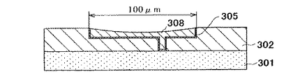
ディッシングは、図27に示すように、例えば、0.18μmルールのデザインルールにおいて、例えば、100μm程度のような幅の広い配線308が存在した場合に、当該配線の中央部が過剰に除去され、へこんでしまう現象であり、このディッシングが発生すると配線308の断面積が不足するため、配線抵抗値不良等の原因となる。このディッシングは、配線材料に比較的軟質の銅やアルミニウムを用いた場合に発生しやすい。
エロージョンは、図28に示すように、例えば、3000μmの範囲に1.0μmの幅の配線が50パーセントの密度で形成されているようなパターン密度の高い部分が過剰に除去されてしまう現象であり、エロージョンが発生すると、配線の断面積が不足するため、配線抵抗値不良等の原因となる。
リセスは、図29に示すように、層間絶縁膜302と配線308との境界で配線308が低くなり段差ができてしまう現象であり、この場合にも配線の断面積が不足するため、配線抵抗値の不良等の原因となる。
【0011】
一方、余分な銅膜307をCMP法によって、平坦化および除去する工程では、銅膜を効率的に除去する必要があるため、単位時間当たりの除去量である研磨レートは、例えば、500nm/min以上となるように要求されている。
この研磨レートを稼ぐためには、ウェーハに対する加工圧力を大きくする必要があり、加工圧力を大きくすると、図30に示すように、配線表面にスクラッチSCやケミカルダメージCDが発生しやすくなり、特に、軟質の銅では発生しやすい。このため、配線のオープン、ショート、配線抵抗値不良等の不具合の原因となり、また、加工圧力を大きくすると、上記のスクラッチ、層間絶縁膜の剥離、ディッシング、エロージョンおよびリセスの発生量も大きくなるという不利益が存在した。
【0012】
本発明は上記の問題点に鑑みてなされたものであり、従って、本発明は、金属膜を研磨によって平坦化する際に、初期凹凸を容易に平坦化でき、かつ余分な金属膜の除去効率に優れ、金属膜へのダメージを抑制可能な研磨装置を提供することを目的とする。
【0013】
【課題を解決するための手段】
上記の目的を達成するため、本発明の研磨装置は、被研磨面に銅膜を有する被研磨対象物を研磨する研磨装置であって、研磨面を有する導電性の研磨工具と、前記研磨工具を所定の回転軸を中心に回転させ、かつ保持する研磨工具回転保持手段と、前記被研磨対象物を保持し所定の回転軸を中心に回転させる被研磨対象物回転保持手段と、前記研磨工具を前記被研磨対象物の前記被研磨面に対して略垂直な方向に移動位置決めする移動位置決め手段と、前記被研磨面と前記研磨面とを所定の平面に沿って相対移動させる相対移動手段と、前記被研磨面上にキレート剤を含む電解液を供給する電解液供給手段と、前記被研磨面を陽極とし前記研磨工具を陰極として、前記被研磨面から前記電解液を通じて前記研磨工具に流れる電流を供給する電流供給手段とを備え、前記電流供給手段は、前記被研磨面に接触可能または接近可能に配置され、前記被研磨面を陽極として通電する陽極部材、および前記陽極部材と前記研磨工具との間に所定電圧を印加する電源を有し、前記研磨工具は、環状形状を有し、その環状の一端面が研磨面を構成しており、前記陽極部材は、前記研磨工具の環の内側に非接触で設けられ、前記研磨工具回転保持手段によって前記研磨工具とともに回転し、保持されるものである。
【0014】
上記の本発明の研磨装置によれば、例えば被研磨対象物の被研磨面に凹凸のある銅膜が形成されている場合に、電流供給手段により、被研磨面の銅膜表面が、陽極酸化され、当該陽極酸化された銅が電解液供給手段によって供給される電解液中のキレート剤により、キレート化され、容易に除去可能な機械的強度の非常に低いキレート膜が形成される。
移動位置決め手段によって、被研磨面に研磨面を接触もしくは接近させ、研磨工具回転保持手段および回転保持手段によって、研磨面および被研磨面を接触もしくは接近した状態でそれぞれ回転させることによって、キレート膜の凸部分が除去され、さらに、相対移動手段により、被研磨面全体におけるキレート膜の凸部分を研磨除去することにより、低い研磨圧力で効率的に被研磨対象物を研磨することができる。
【0015】
また、陽極部材により電解液を通じて局所的に銅膜に電流を流すことにより、安定した電流供給を行うことができる。この場合には、陽極部材から電解液を介して被研磨面に通電され、さらに被研磨面から電解液を通じて研磨工具へと通電されることから、陰極である研磨工具近傍の銅膜が陽極酸化され、キレート化される。
【0016】
本発明の研磨装置は、好適には、前記電源は、所定周期のパルス状の電圧を出力する。
例えば、パルス幅を非常に短くすることで、1パルス当たりの陽極酸化によるキレート膜生成量を非常に小さくして、表面の凹凸に接触した場合など電極間距離の急変による放電、気泡やパーティクルなどが介在した場合に起こる電気抵抗の急変によるスパーク放電など、銅膜の突発的かつ巨大な陽極酸化を防止し、できるだけ小さなものの連続にするために有効なものとなる。
【0017】
本発明の研磨装置は、好適には、前記陽極部材は、前記被研磨面に形成された銅に比して貴なる金属からなる。これにより、陽極部材の電解液への溶出などを防止し、銅膜を積極的に陽極酸化させることができる。なお、本来、陰極は溶出しないため、貴卑を考慮する必要はない。
【0018】
本発明の研磨装置は、好適には、前記被研磨面から前記研磨工具に流れる電流の値を検出する電流検出手段と、前記電流検出手段からの検出信号に基づいて、前記電流の値が一定となるように前記研磨工具の前記被研磨面に対して略垂直方向の位置を制御する制御手段とをさらに有する。
電流値を一定に制御することにより、電流密度は常に一定となり、陽極酸化によるキレート膜生成量も一定に制御することができる。
【0021】
さらに、上記の目的を達成するため、本発明の研磨装置は、被研磨対象物を保持する保持手段と、前記被研磨面に平行に配置される電極板と、前記被研磨対象物に接続された、パルスジェネレータ、アンプおよび加振器からなる加振手段と、研磨砥粒を含まず、キレート剤を含む電解液と、前記電解液を貯留する水槽と、前記被研磨面を陽極とし前記電極板を陰極として、前記被研磨面から前記電解液を通じて前記電極板に流れる電解電流を供給する電解電流供給手段とを備え、前記電解電流供給手段は、20〜50msec毎にパルス状の電圧を出力し、前記被研磨対象物の前記保持手段および前記電極板は前記電解液中に浸漬されて配置され、前記銅膜が前記キレート剤と反応してキレート膜が形成されるように、前記電解電流供給手段が前記電解電流を供給し、前記キレート膜の凸部が除去されるように前記加振手段が前記被研磨対象物を振動させるものである。
【0022】
上記の本発明の研磨装置によれば、例えば被研磨対象物の被研磨面に凹凸のある銅膜が形成されている場合に、電解電流供給手段により、被研磨面の銅膜表面が、陽極酸化され、当該陽極酸化された銅が電解液供給手段によって供給される電解液中のキレート剤により、キレート化され、容易に除去可能な機械的強度の非常に低いキレート膜が形成される。
当該キレート膜の凸部は、加振手段による被研磨対象物への振動作用により選択的に除去され、被研磨対象物へのダメージの少ない効率的な研磨を達成することができる。
【0025】
さらに、上記の目的を達成するため、本発明の研磨装置は、被研磨面に金属膜を有する被研磨対象物を研磨する研磨装置であって、前記被研磨対象物の前記被研磨面を払拭する、通気孔が設けられたワイピング部材と、前記被研磨面に対向し、前記ワイピング部材の上面に配設された対向電極と、前記対向電極および前記ワイピング部材を所定の回転軸を中心に回転させ、かつ保持するワイピング部材回転保持手段と、前記被研磨対象物を保持し所定の回転軸を中心に回転させる被研磨対象物回転保持手段と、前記被研磨面上に電解液を供給する電解液供給手段と、前記被研磨面と前記対向電極間に電流を供給する電流供給手段と、前記ワイピング部材回転保持手段を貫通して前記対向電極および前記ワイピング部材の中心部に垂直に接続された、貫通孔を有し、前記電流を通電する通電軸とを備え、前記電解液は、前記電解液供給手段から前記貫通孔を経由し、前記ワイピング部材を通過して前記被研磨面上に供給されるものである。
【0026】
さらに、上記の目的を達成するため、本発明の研磨装置は、前記被研磨面と前記ワイピング部材とを相対移動させる相対移動手段をさらに有する。
【0027】
前記相対移動手段は、前記被研磨面に前記ワイピング部材を押圧し、前記被研磨面上に前記ワイピング部材を水平移動させる。あるいは、前記相対移動手段は、前記ワイピング部材の前記被研磨面側の面上に前記被研磨面が位置されるように前記被研磨対象物回転保持手段を水平移動させる。
【0028】
上記の本発明の研磨装置によれば、例えば被研磨対象物の被研磨面に金属膜が形成されている場合に、電解液供給手段により、被研磨対象物表面上に電解液が供給され、電流供給手段により被研磨対象物表面と前記対向電極間に電流が供給されることで、被研磨面の金属膜が陽極酸化されてイオン状態となり、容易に除去可能な機械的強度の非常に低い状態となる。
そして、陽極酸化された金属膜の表面をワイパにより払拭することで、陽極酸化された金属膜が除去されることから、低い押圧で効率的に被研磨対象物を研磨することができる。
【0029】
【発明の実施の形態】
以下に、本発明の実施の形態について、図面を参照して説明する。
【0030】
第1実施形態
(半導体装置の製造方法および研磨方法)
本発明の実施形態について、一例として半導体装置の製造工程におけるデュアルダマシン法による金属配線形成プロセスに適用する場合について説明する。
【0031】
まず、図1(a)に示すように、例えば不図示の不純物拡散領域が適宜形成されている、例えばシリコン等の半導体基板101上に、例えばシリコン酸化膜からなる層間絶縁膜102を、例えば反応源としてTEOS(tetraethylorthosilicate )等を用いて減圧CVD(Chemical Vapor Deposition)法により形成する。
なお、層間絶縁膜102としては、CVD法により形成されるTEOS(tetraethylorthosilicate )膜やシリコン窒化膜の他、いわゆるLow−k(低誘電率膜)材料等を用いることができる。
ここで、低誘電率絶縁膜としては、SiF、SiOCH、ポリアリールエーテル、ポーラスシリカ、ポリイミド等がある。
【0032】
次に、図1(b)に示すように、半導体基板101の不純物拡散領域に通じるコンタクトホールCHおよび配線用溝Mを、例えば公知のフォトリソグラフィー技術およびエッチング技術を用いて形成する。なお、配線用溝Mの深さは、例えば、800nm程度である。
【0033】
次に、図1(c)に示すように、バリヤ膜103を層間絶縁膜102の表面、コンタクトホールCHおよび配線用溝M内に形成する。
このバリヤ膜103は、例えば、Ta、Ti、W、Co、Si、Ni、およびそれらの金属とリンあるいは窒素からなるTaN、TiN、WN、CoW、CoWP、TiSiN、NiWP等の合金、およびそれらの積層膜で構成される。これらの材料からなるバリア膜は、既知のスパッタリング装置、真空蒸着装置等をもちいたPVD(Physical Vapor Deposition )法あるいはCVD法により、例えば25nm程度の膜厚で形成する。
バリヤ膜103は、配線を構成する材料が層間絶縁膜102中に拡散するのを防止するため、および、層間絶縁膜102との密着性を上げるために設けられる。例えば、配線材料が銅で層間絶縁膜102が酸化シリコンのような場合には、銅は酸化シリコンへの拡散係数が大きく酸化されやすいため、これを防止する必要がある。
【0034】
次に、図2(d)に示すように、バリヤ膜103上に、配線形成材料と同じ材料からなるシード膜104を公知のスパッタ法により、例えば150nm程度の膜厚で形成する。シード膜104は、後に電解メッキを行うために形成するものであり、例えば金属膜を配線用溝MおよびコンタクトホールCH内に埋め込んだ際に、金属膜の成長を促すために形成する。
【0035】
次に、図2(e)に示すように、コンタクトホールCHおよび配線用溝Mを埋め込むように、バリヤ膜103上にAl、W、WN、Cu、Au、Ag等あるいはそれらの合金膜からなる配線用層105を、例えば1600nm程度の膜厚で形成する。配線用層105は、好ましくは、電解メッキ法または無電解メッキ法によって形成するが、CVD法、PVD法、スパッタ法などによって形成してもよい。なお、シード膜104は配線用層105と一体化する。
配線用層105の表面には、コンタクトホールCHおよび配線用溝Mの埋め込みによって生じた、例えば、800nm程度の高さの凹凸が形成されている。
なお、以下では、例えば配線用層として銅を積層させた場合について説明する。
【0036】
以上のプロセスは、従来と同様のプロセスで行われるが、本発明の研磨方法では、層間絶縁膜102上に存在する余分な配線用層105の除去を化学機械研磨でなく、電解作用を用いた電解複合研磨によって行う。具体的には、電解作用により銅膜を陽極酸化し、表面にキレート膜を形成する。なお、本願発明における研磨とは、削り取る機能、磨く機能、擦る機能、拭き取る機能と広く定義する。
【0037】
キレート膜の形成方法は、図3(f)に示すように、陰極部材120を銅膜105に平行に配置し、電解質、および添加剤として例えば銅をキレート化するキレート剤を含む電解液ELを陰極部材120と銅膜105との間に介在させる。なお、図4以降は、陰極部材120および電解液ELの図中への記載を省略してある。
また、電解液ELには、上記の他、添加剤として、光沢剤、Cuイオン等を含めることができる。
そして、この電解液を温度コントロールして、金属膜表面の酸化、キレート形成割合、払拭割合等を最適化する。
ここで、キレート剤としては、例えば、化学構造式(1)のキナルジン酸、化学構造式(2)のグリシン、化学構造式(3)のクエン酸、化学構造式(4)のシュウ酸、化学構造式(5)のプロピオン酸などを用いる。
次に、陰極部材120を陰極として、銅膜105およびバリヤ膜103を陽極として、電圧を印加する。
【0038】
【化1】

【化2】
NH2 CH2 COOH (2)
【0040】
【化3】
【化4】
(COOH)2 (4)
【0042】
【化5】
C2 H5 COOH (5)
【0043】
陽極である銅膜105は、陽極酸化されることにより、CuOを形成する。ここで、銅膜105表面の凸部と陰極部材120との距離d1は、銅膜105表面の凹部と陰極部材120との距離d2に比して、短いことから、陰極部材120と銅膜105の電位差が一定の場合には、凸部における電流密度の方が凹部に比して大きくなるため、陽極酸化が促進される。
【0044】
図3(g)に示すように、陽極酸化された銅膜(CuO)105の表面は、電解溶液中のキレート剤により、キレート化される。キレート剤にキナルジン酸を用いた場合には、化学構造式(6)のキレート化合物からなる膜となり、グリシンを用いた場合には、化学構造式(7)のキレート化合物からなる膜となる。これらのキレート膜106は、電気抵抗が銅に比して高く、機械的強度は非常に小さい。従って、銅膜105の表面にキレート膜106が形成された後は、銅膜105から電解液ELを通じて陰極部材120へ流れる電流値は低下する。陽極酸化されない前は、銅のキレート化は抑制された状態にある。
【0045】
【化6】
【化7】
次に、図4(h)に示すように、銅膜105の表面に形成されたキレート膜106の凸部を、ワイピング、機械研磨などによって選択的に除去する。なお、機械研磨によって、キレート膜106の凸部を除去する場合に、あらかじめ、電解液ELに不図示のスラリーを含ませていても良い。また、当該キレート膜の機械的強度は非常に小さいため、基板101に振動を与えたり、電解液ELに噴流を与えたりすることによってもキレート膜106を容易に除去することができる。
このとき、電気抵抗の低い銅膜105の凸部が電解液中に露出するため、銅膜105から電解液ELを通じて陰極部材120へ流れる電流値は増加する。
【0048】
次に、図4(i)に示すように、電解液中に露出した銅膜105の凸部は、電気抵抗が低いこと、および陰極部材120との距離が短いことから集中的に陽極酸化され、陽極酸化された銅は、キレート化される。このとき、銅膜105から電解液ELを通じて陰極部材120へ流れる電流値は再び低下する。
その後、キレート膜106の凸部を上述したワイピング、機械研磨などにより、選択的に除去し、露出した銅膜105が集中的に陽極酸化、キレート化され、当該キレート膜106の凸部を選択的に除去する工程を繰り返す。このとき、銅膜105から電解液ELを通じて陰極部材120へ流れる電流値は、キレート膜106の除去と同時に増加し、キレート膜106の形成と同時に低下するという状態を繰り返す。
【0049】
次に、図5(j)に示すように、上記の工程の後、銅膜105が平坦化する。平坦化された当該銅膜105をワイピング、機械研磨等によって全面に除去することにより、銅膜105から電解液ELを通じて陰極部材120へ流れる電流値は、1度最大値をとる。
【0050】
次に、図5(k)に示すように、平坦化された銅膜105の全面について、陽極酸化による生成キレート膜の除去工程を、バリヤ膜103上の余分な銅膜105がなくなるまで続ける。
【0051】
次に、図5(l)に示すように、当該銅膜105の全面を例えば上述したワイピング、機械研磨などにより除去し、バリヤ膜103の表面を露出させる。このとき、銅膜105より電気抵抗の高いバリヤ膜103が露出するため、キレート膜106除去後の電流値の値が低下し始める。当該電流値が低下し始めた時点(終点付近)で、印加電圧を小さくし、その後、電圧を印加するのを停止し、陽極酸化によるキレート化の進行を止める。ここまでのプロセスによって、銅膜105の初期凹凸の平坦化は達成される。
その後、配線用溝の外部に堆積されたバリヤ膜103を除去することにより、銅配線が形成される。
【0052】
本実施形態に係る研磨方法によれば、電気化学的に研磨レートをアシストされた研磨であるため、通常の化学機械研磨に比して、低い加工圧力で研磨を行うことができる。このことは、単純な機械研磨と比較してもスクラッチの低減、段差緩和性能、ディッシングやエロージョンの低減などの面で非常に有利である。
また、低い加工圧力で研磨を行うことができるため、機械強度が弱く通常の化学機械研磨では破壊されてしまい易い、有機系の低誘電率膜や多孔質低誘電率絶縁膜を層間絶縁膜102に用いる場合に非常に有用である。
【0053】
通常の化学機械研磨で、アルミナ粒子などを含むスラリーを使用した場合には、CMP加工に寄与したのち磨滅せずに残留したり、銅表面に埋没することが起こる(パーティクル)が、本発明の研磨方法では、砥粒を含まないキレート剤を電解液とする機械的研磨もしくはワイピングなどでも、表面に形成されたキレート膜は機械的強度が非常に小さいため、十分に除去可能である。
また、電解電流をモニタリングすることで、研磨プロセスの管理を行うことができ、研磨プロセスの進行状態を正確に把握することが可能となる。
【0054】
本発明に係る研磨方法は、上記の実施の形態に限定されない。
銅以外にも、上述したように、例えば、Al、W、WN、Cu、Au、Ag等あるいはそれらの合金膜からなる配線層に適用することができ、上述した材料等からなるバリア膜の研磨にも適用することができる。
また、配線等以外に使用される種々の金属膜の研磨に適用することができる。
また、キレート剤の種類や、陰極部材の種類など、本発明の要旨を逸脱しない範囲で種々の変更が可能である。
また、本発明に係る半導体装置の製造方法は上記の実施の形態に限定されない。
例えば、金属膜の研磨方法以外に係る方法は何ら限定はなく、本実施形態においては、デュアルダマシン法を例に説明したが、シングルダマシン法にも適用でき、その他、コンタクトホールもしくは配線用溝の形成方法や銅膜の形成方法、バリヤ膜の形成方法などは、本発明の要旨を逸脱しない範囲で種々の変更が可能である。
【0055】
(研磨装置)
図6は、本発明の実施形態に係る研磨装置の構成を示す図である。
図6に示す研磨装置は、加工ヘッド部と、電解電源61と、研磨装置全体を制御する機能を有するコントローラー55と、スラリー供給装置71と、電解液供給装置81とを備えている。
なお、図示しないが研磨装置は、クリーンルーム内に設置され、当該クリーンルーム内には、被研磨対象物のウェーハを収納したウェーハカセットを搬出入する搬出入ポートが設けられている。さらに、この搬出入ポートを通じてクリーンルーム内に搬入されたウェーハカセットと研磨装置との間でウェーハの受け渡しを行うウェーハ搬送ロボットが搬出入ポートと研磨装置の間に設置される。また、当該研磨装置により研磨された後のウェーハを洗浄するための洗浄機構が1ユニットとして構成されていてもよい。
【0056】
加工ヘッド部は、研磨工具11を保持し、回転させる研磨工具保持部(研磨工具回転保持手段)10と、研磨工具保持部10をZ軸方向の目標位置に位置決めするZ軸位置決め機構部(移動位置決め手段)30と、被研磨対象物のウェーハWを保持し回転させX軸方向に移動するX軸移動機構部(回転保持手段および相対移動手段)40とから構成されている。
【0057】
Z軸位置決め機構部30は、不図示のコラムに固定されたZ軸サーボモータ31と、Z軸サーボモータ31に接続されたボールネジ軸31aと、保持装置13および主軸モータ14に連結され、ボールネジ軸31aに螺合するネジ部を有するZ軸スライダ32と、Z軸スライダ32をZ軸方向に移動自在に保持する不図示のコラムに設置されたガイドレール33とを有する。
【0058】
Z軸サーボモータ31は、Z軸サーボモータ31に接続されたZ軸ドライバ51から駆動電流が供給されて回転駆動される。ボールネジ軸31aは、Z軸方向に沿って設けられ、一端がZ軸サーボモータ31に接続され、他端は、上記の不図示のコラムに設けられた保持部材によって、回転自在に保持され、その間に、Z軸スライダ32のネジ部と螺合されている。
上記の構成により、Z軸サーボモータ31の駆動により、ボールネジ軸31aが回転され、Z軸スライダ32を介して、研磨工具保持部10に保持された研磨工具11がZ軸方向の任意の位置に移動位置決めされる。Z軸位置決め機構部30の位置決め精度は、例えば分解能0.1μm程度としている。
【0059】
X軸移動機構部40は、ウェーハWをチャッキングするウェーハテーブル42とウェーハテーブル42を回転駆動させる駆動力を供給する駆動モータ44と、駆動モータ44と保持装置45の回転軸とを連結するベルト46と、保持装置45に設けられた加工パン47と、駆動モータ44および保持装置45が設置されたX軸スライダ48と、不図示の架台に設置されたX軸サーボモータ49と、X軸サーボモータ49に接続されたボールネジ軸49aと、X軸スライダ48に連結されボールネジ軸49aに螺合するネジ部が形成された可動部材49bとから構成されている。
【0060】
ウェーハテーブル42は、例えば、真空吸着手段によってウェーハWを吸着する。
加工パン47は、使用済の電解液や、スラリー等の液体を回収するために設けられている。
駆動モータ44は、テーブルドライバ53に接続されており、当該テーブルドライバ53から駆動電流が供給されることによって駆動され、この駆動電流を制御することでウェーハテーブル42を所定の回転数で回転させることができる。
X軸サーボモータ49は、X軸ドライバ54に接続されており、当該X軸ドライバ54から供給される駆動電流によって回転駆動し、X軸スライダ48がボールネジ軸49aおよび可動部材49bを介してX軸方向に駆動する。このとき、X軸サーボモータ49に供給する駆動電流を制御することによって、ウェーハテーブル42のX軸方向の速度制御が可能となる。
【0061】
スラリー供給装置71は、スラリーを不図示の供給ノズルを介して、ウェーハW上に供給する。スラリーとしては、例えば、過酸化水素、硝酸鉄、ヨウ素酸カリウム等をベースとした酸化力のある水溶液に酸化アルミニウム(アルミナ)、酸化セリウム、シリカ、酸化ゲルマニウム等を研磨砥粒として含有させたものを使用する。なお、スラリーは必要に応じて供給すればよい。
【0062】
電解液供給装置81は、電解質と添加剤を含む電解液ELを不図示の供給ノズルを介して、ウェーハW上に供給する。
電解質は、有機溶媒あるいは水溶液をベースとしたものを用いることができる。
電解質は、酸として、例えば、硫酸銅、硫酸アンモニウム、リン酸等があり、アルカリの例としては、エチルジアミン、NaOH、KOH等がある。
また、電解質として、メタノール、エタノール、グリセリン、エチレングリコール等の有機溶媒希釈混合液を用いることもできる。
添加剤としては、Cuイオン、光沢剤またはキレート剤を含む。
光沢剤としては、例えば、イオウ系、水酸化銅やリン酸銅等の銅イオン系、塩酸等の塩素イオン系、ベンゾトリアゾール(BTA)、ポリエチレングリコール等を用いることができる。
キレート剤としては、例えば、上述したキナルジン酸、グリシン、クエン酸、シュウ酸、プロピオン酸などの他、キノリン、アントラニル酸等を用いる。
【0063】
図7は、本実施形態に係る研磨装置の研磨工具保持部10の内部構造を示す図である。
研磨工具保持部10は、研磨工具11と、研磨工具11を保持するフランジ部材12と、フランジ部材12を主軸13aを介して回転自在に保持する保持装置13と、保持装置13に保持された主軸13aを回転させる主軸モータ14と、主軸モータ14上に設けられたシリンダ装置15から構成されている。
【0064】
主軸モータ14は、例えば、ダイレクトドライブモータからなり、このダイレクトドライブモータの不図示のロータは、主軸13aに連結されている。
また、主軸モータ14は、中心部にシリンダ装置15のピストンロッド15bが挿入される貫通孔を有している。主軸モータ14は、主軸ドライバ52から供給される駆動電流によって駆動される。
【0065】
保持装置13は、例えば、エアベアリングを備えており、このエアベアリングで主軸13aを回転自在に保持している。保持装置13の主軸13aも中心部にピストンロッド15bが挿入される貫通孔を有している。
【0066】
フランジ部材12は、金属材料から形成されており、主軸13aに連結され、開口部12aを備え、下端面12bに研磨工具11が固着されている。
フランジ部材12の上端面12c側は、主軸13aに連結されているため、主軸13aの回転によってフランジ部材12も回転する。
フランジ部材12の上端面12cは、主軸モータ14および保持装置13の側面に設けられた導電性の通電部材28(陰極通電部材)に固定された通電ブラシ27と接触しており、通電ブラシ27とフランジ部材12とは電気的に接続されている。
【0067】
シリンダ装置15は、主軸モータ14のケース上に固定されており、ピストン15aを内蔵しており、ピストン15aは、例えば、シリンダ装置15内に供給される空気圧によって矢印A1およびA2のいずれかの向きに駆動される。
このピストン15aには、ピストンロッド15bが連結されており、ピストンロッド15bは、主軸モータ14および保持装置13の中心を通って、フランジ部材12の開口部12aから突き出ている。
ピストンロッド15bの先端には、押圧部材21が連結されており、この押圧部材21はピストンロッド15bに対して所定の範囲で姿勢変更が可能な連結機構によって連結されている。
押圧部材21は、対向する位置に配置された絶縁板22の開口22aの周縁部に接触可能となっており、ピストンロッド15bの矢印A2方向への駆動によって絶縁板22を押圧する。
【0068】
シリンダ装置15のピストンロッド15bの中心部には、貫通孔が形成されており、貫通孔内に通電軸20が挿入され、ピストンロッド15bに対して固定されている。
通電軸20は、導電性材料から形成されており、上端側はシリンダ装置15のピストン15aを貫通してシリンダ装置15上に設けられたロータリジョイント16まで伸びており、下端側は、ピストンロッド15bおよび押圧部材21を貫通して電極板23まで伸びており、電極板23に接続されている。
【0069】
通電軸20は、中心部に貫通孔が形成されており、この貫通孔が化学研磨剤(スラリー)およびキレート剤を含む電解液をウェーハW上に供給する供給ノズルとなっている。
また、通電軸20は、ロータリジョイント16と、電極板23とを電気的に接続する役割を果たしている。
【0070】
ロータリジョイント16は、電解電源61のプラス極と電気的に接続されており、通電軸20が回転しても通電軸20への通電を維持する。
【0071】
通電軸20の下端部に接続された電極板(陽極部材)23は、金属材料からなり、特に、ウェーハWに形成される例えば銅等の金属膜と同等または金属膜より貴なる金属で形成されている。
電極板23は、上面側が絶縁板22に保持されており、電極板23の外周部は絶縁板22に嵌合しており、下面側にはスクラブ部材24が貼着されている。
【0072】
絶縁板22は、例えば、セラミクス等の絶縁材料から形成されており、この絶縁板22は複数の棒状の連結部材26によって主軸13aに連結されている。連結部材26は、絶縁板22の中心軸から所定の半径位置に等間隔に配置されており、主軸13aに対して移動自在に保持されている。このため、絶縁板22は主軸13aの軸方向に移動可能である。
また、絶縁板22と主軸13aとの間には、各連結部材26に対応して、例えば、コイルスプリングからなる弾性部材25で接続されている。
【0073】
絶縁板22を保持装置13の主軸13aに対して移動自在にし、絶縁板22と主軸13aとを弾性部材25で連結する構成とすることにより、シリンダ装置15に高圧エアを供給してピストンロッド15bを矢印A2の向きに下降させると、押圧部材21が弾性部材25の復元力に逆らって絶縁板22を下方に押し下げ、これとともにスクラブ部材24も下降する。
この状態からシリンダ装置15への高圧エアの供給を停止すると、弾性部材25の復元力によって、絶縁板22は上昇し、これとともにスクラブ部材24も上昇する。
【0074】
研磨工具11は、フランジ部材12の環状の下端面12bに固着されている。この研磨工具11は、ホイール状に形成されており、下端面に環状の研磨面11aを備えている。研磨工具11は、導電性を有しており、好ましくは、比較的軟質性の材料で形成する。例えば、バインダマトリクス(結合剤)自体が導電性を持つカーボンや、あるいは、焼結銅、メタルコンパウンド等の導電性材料を含有するウレタン樹脂、メラミン樹脂、エポキシ樹脂、ポリビニルアセタール(PVA)などの樹脂からなる多孔質体から形成することができる。
研磨工具11は、導電性を有するフランジ部材12に直接接続され、フランジ部材12に接触する通電ブラシ27から通電される。
すなわち、主軸モータ14および保持装置13の側面に設けられた導電性の通電部材28は、電解電源61のマイナス極と電気的に接続され、通電部材28に設けられた通電ブラシ27はフランジ部材12の上端面12cに接触しており、これにより、研磨工具11は電解電源61と通電部材28、通電ブラシ27およびフランジ部材12を介して電気的に接続されている。
【0075】
電解電源(電流供給手段)61は、上記したロータリジョイント16と通電部材(陰極通電部材)28との間に所定の電圧を印加する装置である。ロータリジョイント16と通電部材28との間に電圧を印加することによって、研磨工具11とスクラブ部材24との間には電位差が発生する。
電解電源61には、常に一定の電圧を出力する定電圧電源ではなく、好ましくは、電圧を一定周期でパルス状に出力する、例えば、スイッチング・レギュレータ回路を内蔵した電源を使用する。
具体的には、パルス状の電圧を一定周期で出力し、パルス幅を適宜変更可能な電源を使用する。一例としては、出力電圧がDC2〜5V、最大出力電流が2〜3A、パルス幅が1,2,5,10,20,50msecのいずれかに変更可能なものを使用する。
上記のような幅が短いパルス状の電圧出力とするのは、1パルス当たりの陽極酸化量を非常に小さくするためである。すなわち、ウェーハWの表面に形成された例えば銅等の金属膜の凹凸に接触した場合などにみられる極間距離の急変による放電、気泡やパーティクルなどが介在した場合におこる電気抵抗の急変によるスパーク放電など、金属膜の突発的かつ巨大な陽極酸化を防止し、できる限り小さなものの連続にするために有効である。
また、出力電流に比して出力電圧が比較的高いため、極間距離の設定にある程度のマージンを設定する事ができる。すなわち、極間距離が多少変わっても出力電圧が高いため電流値変化は小さい。
なお、印加するパルスとしては、上記に限られるものでなく、周期性パルスとして矩形パルス、サイン波形、鋸歯状波形、PAM波形を印加してもよい。
【0076】
電解電源61には、本発明の電流検出手段としての電流計62を備えており、この電流計62は、電解電源61に流れる電解電流をモニタするために設けられており、モニタした電流値信号62sをコントーラ55に出力する。
また、電解電源61は、電流検出手段に変わって抵抗値検出手段としての抵抗計を備えていてもよく、その役割は電流検出手段と同様である。
【0077】
コントローラ55は、研磨装置の全体を制御する機能を有し、具体的には、主軸ドライバ52に対して制御信号52sを出力して研磨工具11の回転数を制御し、Z軸ドライバ51に対して制御信号51sを出力して研磨工具11のZ軸方向の位置決め制御を行い、テーブルドライバ53に対して制御信号53sを出力してウェーハWの回転数を制御し、X軸ドライバ54に対して制御信号54sを出力して、ウェーハWのX軸方向の速度制御を行う。
また、コントローラ55は、電解液供給装置81およびスラリー供給装置71の動作を制御し、電解液ELおよびスラリーSLの供給動作を制御する。
【0078】
また、コントローラ55は、電解電源61の出力電圧、出力パルスの周波数、出力パルスの幅等を制御可能となっている。
また、コントローラ55には、電解電源61の電流計62からの電流値信号62sが入力される。コントローラ55は、これら電流値信号62sに基づいて、研磨装置の動作を制御可能となっている。具体的には、電流値信号62sから得られる電解電流が一定となるように、電流値信号62sをフィードバック信号としてZ軸サーボモータ31を制御したり、電流値信号62sで特定される電流値に基づいて、研磨加工を停止させるように研磨装置の動作を制御する。
陰極部材と前記金属膜を流れる電流がステップ状に変化するように設定された周期性パルスを印加することが可能であり、例えば金属膜除去の初期においては、陰極部材と金属膜を流れる電流が徐々に増加するように設定された周期性パルスを印加する。これにより、電圧印加開始時などにおいて瞬間的に高電圧が印加されてしまい、除去される金属膜の表面状態が劣化するのを防止することができる。
また、金属膜除去の終点付近では、電流値信号62sが小さくなることから、所定のしきい値と比較して、当該しきい値よりも電流値信号62sが小さくなった場合には、終点付近であるとして出力パルスを小さくするように制御し、その後、パルスの出力を止めるように電解電源61へ制御信号を出力する。
【0079】
コントローラ55に接続されたコントロールパネル56は、オペレータが各種のデータを入力したり、例えば、モニタリングした電流値信号62sを表示したりする。
【0080】
ここで、図8(a)は電極板23の構造の一例を示す下面図であり、図8(b)は電極板23と、通電軸20、スクラブ部材(洗浄部材)24および絶縁板22との位置関係を示す断面図である。
図8(a)に示すように、電極板23の中央部には円形の開口部(供給ノズル)23aが設けられており、この開口部23aを中心に電極板23の半径方向に放射状に伸びる複数の溝部23bが形成されている。
また、図8(b)に示すように、電極板23の開口部23aには、通電軸20の下端部が嵌合固着されている。
【0081】
このような構成とすることで、通電軸20の中心部に形成された供給ノズル20aを通じて供給されるスラリーおよび電解液が、溝部23bを通じてスクラブ部材24の全面に拡散するようになっている。
すなわち、電極板23、通電軸20、スクラブ部材24および絶縁板22が回転しながら、スラリーおよび電解液が供給ノズル20aを通じてスクラブ部材24の上側面に供給されると、スクラブ部材24の上側面全体にスラリーおよび電解液が広がる。
なお、スクラブ部材24および通電軸20の供給ノズル20aが本発明の研磨剤供給手段および電解液供給手段の一具体例に対応している。
【0082】
電極板23の下面に貼着されたスクラブ部材24は、電解液およびスラリーを吸収し、これらを上側面から下側面に通過させることができる材料から形成されている。また、このスクラブ部材24は、ウェーハWに接触してウェーハWをスクラブする面を有しており、ウェーハW表面にスクラッチ等を発生させないように、例えば、柔らかいブラシ状の材料、スポンジ状の材料、多孔質状の材料等から形成される。例えば、ウレタン樹脂、メラミン樹脂、エポキシ樹脂、ポリビニルアセタール(PVA)などの樹脂からなる多孔質体が挙げられる。
【0083】
図9に、研磨する際の研磨工具11とウェーハの位置関係を示す。
研磨工具11の中心軸は、例えばウェーハWに対して微小な角度で傾斜している。また、保持装置13の主軸13aもウェーハWの主面に対して研磨面11aの傾斜と同様に傾斜している。例えば、保持装置13のZ軸スライダ32への取り付け姿勢を調整することで主軸13aの微小な傾斜をつくり出すことができる。
【0084】
このように、研磨工具11の中心軸がウェーハWの主面に対して微小角度で傾斜していることにより、研磨工具11の研磨面11aを所定の加工圧力FでウェーハWに押し付けた際に、実行的な接触面積は一定に維持される。
本実施形態に係る研磨装置では、研磨工具11の一部を部分的に研磨面11aとして、ウェーハWの表面に作用させ、実効的接触領域をウェーハWの表面に均一に走査させてウェーハWの全面を均一に研磨する。
これにより、電解電流の値を一定に制御すれば、電流密度は常に一定とでき、金属膜の陽極酸化によるキレート化の量も常に一定にすることができる。
【0085】
次に、上記した研磨装置による研磨動作(研磨方法)をウェーハW表面に形成された金属膜として例えば銅膜を研磨する場合を例に説明する。図10は、研磨装置において研磨工具11をZ軸方向に下降させ、ウェーハWの表面に接触させた状態を示す概略図である。
まず、ウェーハテーブル42にウェーハWをチャッキングし、ウェーハテーブル42を駆動して所定の回転数でウェーハWを回転させる。
また、ウェーハテーブル42をX軸方向に移動して、フランジ部材12に取り付けられた研磨工具11をウェーハWの上方の所定の場所に配置させ、研磨工具11を所定の回転数で回転させる。研磨工具11を回転させると、フランジ部材12に連結された絶縁板22、電極板23およびスクラブ部材24も回転駆動される。また、スクラブ部材24を押圧している押圧部材21、ピストンロッド15b、ピストン15a、通電軸20も同時に回転する。
【0086】
この状態から、スラリー供給装置71および電解液供給装置81からそれぞれスラリーSLおよび電解液ELを通電軸20内の供給ノズル20aに供給すると、スクラブ部材24の全面からスラリーSLおよび電解液ELが供給される。
研磨工具11をZ軸方向に下降させて研磨工具11の研磨面11aをウェーハWの表面に接触させ、所定の加工圧力で押圧させる。
また、電解電源61を起動させて、通電ブラシ27を通じて研磨工具11にマイナスの電位を印加し、ロータリジョイント16を通じて電極板23およびスクラブ部材24にプラスの電位を印加する。
【0087】
さらに、シリンダ装置15に高圧エアを供給して、図7の矢印A2の方向にピストンロッド15bを下降させ、スクラブ部材24の下面をウェーハWに接触あるいは接近する位置まで移動させる。
この状態からウェーハテーブル42をX軸方向に所定の速度パターンで移動させ、ウェーハWの全面を一様に研磨加工する。
【0088】
図11は図10の円C内の拡大図であり、図12は図11の円D内の拡大図である。
図11に示すように、スクラブ部材24はウェーハWに形成された銅膜MTを、電解液ELを介して、または、直接接触することにより陽極として通電し、研磨工具11もウェーハWに形成された銅膜MTを、電解液ELを介して、または、直接接触することにより陰極として通電する。なお、図11に示すように、銅膜MTとスクラブ部材24との間には、ギャップδb が存在している。さらに、図12に示すように、銅膜MTと研磨工具11の研磨面11aとの間にはギャップδw が存在している。
図11に示すように、絶縁板22は、研磨工具11とスクラブ部材24(電極板23)との間に介在しているが、絶縁板22の抵抗R0は非常に大きく、したがって、スクラブ部材24から絶縁板22を介して研磨工具11に流れる電流i0 はほぼ零であり、スクラブ部材24から絶縁板22を介して研磨工具11には電流が流れない。
【0089】
このため、スクラブ部材24から研磨工具11に流れる電流は、直接電解液EL中の抵抗R1を経由して研磨工具11に流れる電流i1 と、電解液EL中からウェーハWの表面に形成された銅膜MTを経由して再度電解液EL中を通って研磨工具11に流れる電流中に流れる電流i2 に分岐する。
銅膜MTの表面に電流i2 が流れると、銅膜MTを構成する銅は、電解液ELの電解作用によって陽極酸化され、電解液中のキレート剤により、キレート化される。
【0090】
ここで、電解液EL中の抵抗R1は、陽極としてのスクラブ部材24と陰極としての研磨工具11との距離dに比例して極端に大きくなる。このため、極間距離dを、ギャップδb およびギャップδw よりも十分に大きくしておくことで、直接電解液EL中の抵抗R1を経由して研磨工具11に流れる電流i1 は非常に小さくなり、電流i2 が大きくなって、電解電流のほとんどは銅膜MTの表面経由することになる。このため、銅膜MTを構成する銅の陽極酸化によるキレート化を効率的に行うことができる。
また、電流i2 の大きさは、ギャップδb およびギャップδw の大きさによって変化するため、上述したように、コントローラ55によって研磨工具11のZ軸方向の位置制御を行ってギャップδb およびギャップδw の大きさを調整することにより、電流i2 を一定にすることができる。ギャップδw の大きさの調整は、電流値信号62sから得られた電解電流、すなわち、電流i2 が一定となるように、電流値信号62sをフィードバック信号としてZ軸サーボモータ31の制御を行うことで可能である。
また、研磨装置のZ軸方向の位置決め精度は分解能0.1μmと十分に高く、加えて、主軸13aをウェーハWの主面に対して微小角度で傾斜させていることで実行的な接触面積は常に一定に維持されることから、電解電流の値を一定に制御すれば、電流密度は常に一定とでき、銅膜の陽極酸化によるキレート化の量も常に一定にすることができる。
【0091】
以上のように、上記構成の研磨装置は、上述したウェーハWに形成された銅膜MTの表面に、陽極酸化によるキレート膜を生成し、除去する電解研磨機能を備えている。
さらに、上記構成の研磨装置は、この電解研磨機能に加えて、研磨工具11およびスラリーSLによる通常のCMP装置の化学機械研磨機能も備えており、ウェーハWをこれら電解研磨機能および化学機械研磨の複合作用によって研磨すること(以下、電解複合研磨という)もできる。
また、上記構成の研磨装置は、スラリーSLを用いずに研磨工具11の研磨面11aの機械的な研磨と電解研磨機能との複合作用によって研磨加工を行うこともできる。
【0092】
本実施形態に係る研磨装置によれば、電解研磨および化学機械研磨の複合作用によって銅等の金属膜を研磨できるため、化学機械研磨のみ、あるいは、機械研磨のみを用いた研磨装置に比べてはるかに高能率に金属膜の除去を行うことができる。金属膜に対する高い研磨レートが得られるため、研磨工具11のウェーハWに対する加工圧力Fを化学機械研磨のみ、あるいは機械研磨のみを用いた研磨装置に比べて低く抑えることが可能となり、ディッシング、エロージョンの発生を抑制することができる。
【0093】
また、通常の化学機械研磨に用いるスラリーにおいて、アルミナ粒子などを含むスラリーを使用した場合に、研磨後に、スラリーが磨滅せずに金属膜表面に残留したり、埋没することも起こるが、本実施形態に係る研磨装置では、研磨砥粒を含まないキレート剤を含む電解液を使用する機械研磨のみであっても、表面に残存するキレート膜は機械的強度が非常に低いため、十分に除去可能であることから、パーティクルやスラリーのウェーハ表面への残留を防止することができる。
【0094】
さらに、研磨装置のZ軸方向の位置決め精度は分解能0.1μmと十分に高く、加えて、主軸13aをウェーハWの主面に対して微小角度で傾斜させていることで実行的な接触面積は常に一定に維持されることから、電解電流の値を一定に制御すれば、電流密度は常に一定とでき、金属膜の陽極酸化によるキレート化の量も常に一定にすることができる。
上述した実施形態では、金属膜の研磨加工量の絶対値は、電解電流の積算量と研磨工具11のウェーハWを通過する時間で制御できる。
【0095】
変形例1
図13は、本発明に係る研磨装置の一変形例を示す概略図である。
上述した実施形態に係る研磨装置では、ウェーハW表面への通電を、導電性の研磨工具11と、スクラブ部材24を備えた電極板23とによって行った。
図13に示すように、ホイール状の研磨工具311に、上述した研磨装置の場合と同様に導電性を持たせるとともに、ウェーハWをチャッキングし回転させるウェーハテーブル342にも導電性を持たせる構成としてもよい。研磨工具311への給電は、上述した実施形態と同様の構成で行う。
この場合には、ウェーハテーブル342への通電は、ウェーハテーブル342の下部にロータリージョイント316を設け、ロータリージョイント316によって回転するウェーハテーブル342への通電を常に維持する構成とすることで、電解電流の供給を行うことができる。
【0096】
変形例2
図14は、本発明に係る研磨装置の他の変形例を示す概略図である。
ウェーハWをチャッキングし、回転させるウェーハテーブル442は、ウェーハWをウェーハWの周囲に設けたリテーナリング410によって保持している。
研磨工具411には、導電性を持たせるとともに、リテーナリング410にも導電性を持たせ、研磨工具411には上述した実施形態と同様の構成で給電する。
また、リテーナリング410は、ウェーハWに形成された上記のバリア層部分まで覆い通電する。さらに、リテーナリング410には、ウェーハテーブル442の下部に設けられたロータリジョイント416を通じて給電する。
なお、研磨工具411がウェーハWに接触しても、エッジの部分でリテーナリング410の厚さ以上の隙間が維持できるように研磨工具411の傾斜量を大きくしておくことで、研磨工具411とリテーナリング410との干渉を防ぐことができる。
【0097】
変形例3
図15は、本発明に係る研磨装置の他の実施形態を示す概略構成図である。
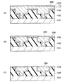
図15に示す研磨装置は、従来型のCMP装置に本発明の電解研磨機能を付加したものであって、定盤201上に研磨パッド(研磨布)202が貼着された研磨工具の研磨面にウェーハチャック207によってチャッキングされたウェーハWの全面を回転させながら接触させてウェーハWの表面を平坦化する研磨装置である。
【0098】
研磨パッド202には、陽極電極204と陰極電極203とが放射状に交互に配置されている。また、陽極電極204と陰極電極203とは絶縁体206によって電気的に絶縁されており、陽極電極204と陰極電極203は、定盤201側から通電される。これら陽極電極204と陰極電極203と絶縁体206とによって研磨パッド202は構成されている。
また、ウェーハチャック207は、絶縁材料から形成されている。
さらに、この研磨装置には、研磨パッド202の表面に電解液ELおよびスラリーSLを供給する供給部208が設けられており、電解研磨および化学機械研磨を複合させた電解複合研磨が可能になっている。
【0099】
ここで、図16は、上記構成の研磨装置による電解複合研磨動作(研磨方法)を説明するための図である。なお、ウェーハW表面には、銅等の金属膜210が形成されているものとする。
図16に示すように、電解複合研磨中には、ウェーハW表面に形成された金属膜210と研磨パッド202の研磨面との間には、電解液ELおよびスラリーSLが介在した状態で、陽極電極204と陰極電極203との間に電圧が印加され、電流iが陽極電極204から電解液ELを通って金属210内を伝って再び電解液ELを通って陰極電極203に流れる。
このとき、図16に示す円G内の付近で、金属膜210の表面は、陽極酸化によりキレート膜を生成し、当該キレート膜は研磨パッド202とスラリーSLによる機械的除去作用によって除去されることにより、金属膜の平坦化が達成される。
【0100】
このような構成とすることにより、上述した実施形態に係る研磨装置と同様の効果が奏される。
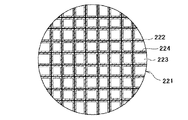
なお、研磨パッドに設ける陽極電極、陰極電極の配置は図15の構成に限定されるわけではなく、例えば、図17に示すように、線状の複数の陽極電極222を縦横に等間隔に配列し、陽極電極222によって囲まれる各矩形領域に陰極電極223を配置し、陽極電極222と陰極電極223とを絶縁体224で電気的に絶縁した研磨パッド221としてもよい。
さらに、例えば、図18に示すように、半径がそれぞれ異なる環状の陽極電極242を同心上に配置し、各陽極電極242間に形成される環状領域に陰極電極243をそれぞれ配置し、陽極電極242と陰極電極243とを絶縁体244で電気的に絶縁した研磨パッド241としてもよい。
【0101】
参考実施形態
図19は本発明の参考実施形態に係る研磨装置の概略構成図である。本実施形態に係る研磨装置は、電解液ELを所定量満たした水槽501と、当該水槽の電解液EL中に配置されたウェーハ保持手段530および電極板510と、水槽の電解液ELを管522により吸い上げて管521により噴流として送り出すジェットポンプ520(流動手段)と、電極板510を陰極としてウェーハを陽極として電圧を印加する電源561(電解電流供給手段)と、電流計562と、コントローラ555およびコントロールパネル556から構成されている。
【0102】
保持手段530は、ウェーハを固定する導電性の第1保持部材531と導電性の第2保持部材532と、不図示のカラムなどに固定され、第1保持部材および第2保持部材を所定の位置に固定するZ軸位置決め機構533とから構成されている。ウェーハの下側に位置する第2保持部材は、円形の開口部532aを有している。
【0103】
電極板510は、電解液EL中にウェーハに平行に配置されており、例えば無酸素銅などにより、構成されている。
【0104】
電解液ELは、第1実施形態と同様のものを使用することができ、例えば銅等の金属をキレート化するキレート剤を含んでおり、その他の添加剤などを含んでいても良い。例えば、電解質として、ウェーハと電極板510の間に印加される電圧を低下させるための、硫酸銅を用いる。
【0105】
電解電源(電解電流供給手段)561には、常に一定の電圧を出力する定電圧電源ではなく、好ましくは、電圧を一定周期でパルス状に出力する電源を使用する。例えば、電解電源561により印加される電圧は、20〜50msec毎に高電圧と低電圧を繰り返す矩形形状のパルス電圧(例えば2〜5V、電流2.2A)である。
【0106】
上記のパルス電圧としては、ウェーハと電極板510との距離dなどにより、最も効率的に金属を除去することができる電圧およびパルス幅を選択することができる。
電極板510とウェーハとの距離dが小さすぎると、電極板510とウェーハとの間に介在する電解液の流動作用が十分に機能しないため、距離dは、所定の値以上を取ることが好ましく、上記の電圧と合わせて設定することが好ましい。
【0107】
電解電源561には、本発明の電流検出手段としての電流計562を備えており、この電流計562は、電解電源561に流れる電解電流をモニタするために設けられており、モニタした電流値信号562sをコントーラ555に出力する。
また、コントローラ555には、電解電源561の電流計562からの電流値信号562sが入力される。コントローラ555は、これら電流値信号562sに基づいて、研磨装置の動作を制御可能となっている。具体的には、電流値信号562sで特定される電流値に基づいて、研磨加工を停止させるように研磨装置の動作を制御する。
【0108】
コントローラ555に接続されたコントロールパネル556は、オペレータが各種のデータを入力したり、例えば、モニタリングした電流値信号562sを表示したりする。
【0109】
上記の研磨装置の構成によっても、第1実施形態に係る研磨装置と同様に、例えばウェーハWの表面に凹凸のある金属膜が形成されている場合に、ウェーハWを陽極として印加することで、ウェーハWの金属膜表面が陽極酸化され、当該陽極酸化された金属膜が電解液EL中のキレート剤によりキレート化され、当該キレートは機械的強度が非常に弱いことから、ジェットポンプ520の管521からの電解液の流動作用によって、当該キレート膜の凸部が除去されることにより、金属膜の平坦化除去が達成される。
また、電解電流をモニタリングすることで、研磨プロセスの管理を行うことができ、研磨プロセスの進行状態を正確に把握することが可能となる。
【0110】
本実施形態に係る研磨装置によれば、機械的強度の非常に低いキレート膜の除去によって、金属膜の除去を達成できることから、従来の化学機械研磨のみ、あるいは、機械研磨のみを用いた研磨装置に比べてはるかに高能率に金属膜の除去を行うことができる。
従来の機械研磨のような強い押圧を必要としないため、配線金属膜下層の層間絶縁膜などに与えるダメージを低く抑えることが可能となり、ディッシング、エロージョンなどの発生を抑制することができる。配線金属膜下層の絶縁膜に高い圧力を印加しないので、該絶縁膜材料として機械的強度がTEOSなどを原料にした酸化シリコンよりも低い低誘電率材料にも適用可能である。
また、研磨装置としては、装置構成が簡便であるので、小型化を容易に実現でき、メンテナンスも容易で稼働率を向上させることができる。
【0111】
さらに、通常の化学機械研磨に用いるスラリーにおいて、アルミナ粒子などを含むスラリーを使用した場合に、研磨後にスラリーが磨滅せずに金属表面に残留したり、埋没することも起こるが、本実施形態に係る研磨装置では、そのような問題はない。
【0112】
本発明は、上記の実施形態に限定されない。例えば、ジェットポンプの構成、電極板の種類、水槽中でのウェーハを保持する装置の構成など、本発明の要旨を逸脱しない範囲で種々の変更が可能である。
【0113】
第2実施形態
図20は本発明の第2実施形態に係る研磨装置の概略構成図である。本実施形態に係る研磨装置では、パルスジェネレータ640、アンプ641、加振器643からなる加振手段と、電解液ELを所定量満たした水槽601と、当該水槽の電解液EL中に配置されたウェーハ保持手段630および電極板610と、電極板610を陰極としてウェーハを陽極として、電圧を印加する電源661(電解電流供給手段)と、電流計662と、コントローラ655およびコントロールパネル656から構成されている。
【0114】
保持手段630は、電極板610をウェーハWに対して平行に保持する第1保持部材631、ウェーハを介在させて圧着して固定する第2保持部材632と第3保持部材634、一端が第2保持部材632に取り付けられており他端が加振器643に取り付けられている第4保持部材633から構成されている。
【0115】
第2保持部材632は、導電性材料から構成されており、ウェーハWを陽極として、通電する役割も果たす。また、第2保持部材632は、ウェーハの表面を電極板610に対して開口するための開口部分632aを有している。
【0116】
電解液ELは、第1実施形態と同様のものを使用することができ、例えば銅等の金属をキレート化するキレート剤を含んでおり、その他の添加剤などを含んでいても良い。例えば、電解質として、ウェーハと電極板510の間に印加される電圧を低下させるための、硫酸銅を用いる。
【0117】
電極板610は、電解液EL中にウェーハに平行に配置されており、例えば無酸素銅などにより、構成されている。
【0118】
電解電源(電解電流供給手段)661には、常に一定の電圧を出力する定電圧電源ではなく、好ましくは、電圧を一定周期でパルス状に出力する電源を使用する。例えば、電解電源661により印加される電圧は、20〜50msec毎に高電圧と低電圧を繰り返す矩形形状のパルス電圧(例えば2〜5V、電流2.2A)である。
【0119】
上記のパルス電圧としては、ウェーハと電極板610との距離dなどにより、最も効率的に金属膜を除去することができる電圧およびパルス幅を選択することができる。
電極板610とウェーハとの距離dが小さすぎると、電極板610とウェーハとの間に介在する電解液の循環作用が十分に機能しないため、距離dは、所定の値以上を取ることが好ましく、上記の電圧と合わせて設定することが好ましい。
【0120】
電解電源661には、本発明の電流検出手段としての電流計662を備えており、この電流計662は、電解電源661に流れる電解電流をモニタするために設けられており、モニタした電流値信号662sをコントーラ655に出力する。また、コントローラ655には、電解電源661の電流計662からの電流値信号662sが入力される。コントローラ655は、これら電流値信号662sに基づいて、研磨装置の動作を制御可能となっている。具体的には、電流値信号662sで特定される電流値に基づいて、研磨加工を停止させるように研磨装置の動作を制御する。
【0121】
コントローラ655に接続されたコントロールパネル656は、オペレータが各種のデータを入力したり、例えば、モニタリングした電流値信号662sを表示したりする。
【0122】
上記の研磨装置の構成によっても、第1実施形態に係る研磨装置と同様に、例えばウェーハWの表面に凹凸のある金属膜が形成されている場合に、ウェーハWを陽極として印加することで、ウェーハWの金属膜表面が陽極酸化され、当該陽極酸化された金属膜が電解液EL中のキレート剤によりキレート化され、当該キレートは機械的強度が非常に弱いことから、加振器643からのウェーハ振動手段によって、当該キレート膜の凸部が除去されることにより、金属膜の平坦化除去が達成される。
また、電解電流をモニタリングすることで、研磨プロセスの管理を行うことができ、研磨プロセスの進行状態を正確に把握することが可能となる。
【0123】
本実施形態に係る研磨装置によれば、機械的強度の非常に低いキレート膜の除去によって、金属膜の除去を達成できることから、従来の化学機械研磨のみ、あるいは、機械研磨のみを用いた研磨装置に比べてはるかに高能率に金属膜の除去を行うことができる。
従来の機械研磨のような強い押圧を必要としないため、配線金属膜下層の層間絶縁膜などに与えるダメージを低く抑えることが可能となり、ディッシング、エロージョンなどの発生を抑制することができる。配線金属膜下層の絶縁膜に高い圧力を印加しないので、該絶縁膜材料として機械的強度がTEOSなどを原料にした酸化シリコンよりも低い低誘電率材料にも適用可能である。
また、研磨装置としては、装置構成が簡便であるので、小型化を容易に実現でき、メンテナンスも容易で稼働率を向上させることができる。
【0124】
さらに、通常の化学機械研磨に用いるスラリーにおいて、アルミナ粒子などを含むスラリーを使用した場合に、研磨後にスラリーが磨滅せずに金属表面に残留したり、埋没することも起こるが、本実施形態に係る研磨装置では、そのような問題はない。
【0125】
本発明は、上記の実施形態に限定されない。例えば、加振器およびアンプの構成、電極板の種類、水槽中でのウェーハを保持する装置の構成など、本発明の要旨を逸脱しない範囲で種々の変更が可能である。
【0126】
第3実施形態
図21に本実施形態に係る研磨装置の要部構成図を示す。基本的構成は、第1実施形態と同様であるが、本実施形態では、研磨工具を使用せず、ワイピング部材24aによりウェーハ上の金属膜を除去する。従って、説明の簡略化のため、第1実施形態と異なる構成のみについて説明する。
【0127】
ワイピング部材24aは、例えば、電気又はイオンが通らない絶縁体で構成されその内部に気孔部を有し、当該気孔部に含有する電解液ELを介してウェーハに通電することができる材料により構成されている。
上記の材料は、電解液ELに侵されない材料である必要がある。
また、ワイピング部材24aは、ウェーハW表面とワイピング部材24aが押圧されてウェーハW表面の金属膜が除去されるため、ワイピング部材は、所定の強度が必要である。
例えば、ウェーハ表面Wの金属膜の凸部のみをワイピングするための圧力を約20〜100g/cm2 とした場合にも耐えうる弾性強度を有するとともに、スクラッチや傷等を発生しない柔らかさを有する硬度が必要である。
【0128】
上記の条件を満たす材料として、弾塑性体材料を使用することができ、例えばポリビニルアセタール(PVA)、発砲ウレタン、テフロン発砲体、テフロン繊維不織布等を使用する。
また、導電性を有していてもよく、比較的軟質性の材料、例えば、バインダマトリクス(結合剤)自体が導電性を持つカーボンや、あるいは、焼結銅、メタルコンパウンド等の導電性材料を含有するウレタン樹脂、メラミン樹脂、エポキシ樹脂、ポリビニルアセタール(PVA)などの樹脂からなる多孔質体を使用することもできる。
【0129】
なお、電極板23は、ウェーハW表面に形成された金属膜よりも貴なる金属により構成され、ウェーハWの表面に対して平行に配置されており、例えば、ウェーハW表面の金属膜の電解作用による被研磨表面から発生したガスを抜くための通気孔を設けることが好ましい。この通気孔は、ガスによる電極板23とウェーハWとの間の電解作用の不均一等の不利益を防止するために設けられる。
また、第1実施形態と同様、電極板23はワイピング部材24aとともに回転駆動可能となっており、これにより電極板23が回転することにより電解作用による被研磨表面から発生したガスをウェーハWと電極板23の間から抜くことが可能である。
また、電極板23は、図17および図18で説明したように電極が領域ごとに分割された構成であってもよく、これにより被研磨表面への電解作用を部分的に選択して行うこともできる。
【0130】
電解電源61は、第1実施形態と同様、上記したロータリジョイント16およびウェーハに接触する通電ブラシ710との間に上記した所定のパルスを印加する。
ここで、本実施形態では、電圧印加方向が逆になっており、従って、通電ブラシ710が陽極、電極板23が陰極となるように電圧を印加する。このように、通電ブラシ710によりウェーハW表面の金属膜に接触して電圧を印加する構成の他、ウェーハW表面の金属膜に接近可能な電極を有して電圧を印加する構成としてもよい。
具体的には、第1実施形態と同様にパルス状の電圧を一定周期で出力し、パルス幅を適宜変更可能な電源であれば特に限定はない。例えば、0Vを中心にプラスとマイナスを所定の周期で繰り返すPR(Periodic Reverse) パルス電圧を印加する。このPRパルス電圧として、例えば、出力電圧が0.8〜1.2V程度の正電圧と−0.8〜−1.2V程度の逆電圧を繰り返し、電流密度が正流が10mA/cm2 で逆流が10mA/cm2 程度、パルス幅が正流パルスが20〜50msecで逆流パルスが5〜10msec程度のものを使用する。
なお、印加するパルスとしては、上記に限られるものでないことは第1実施形態と同様である。
【0131】
通電ブラシ710は、ウェーハW表面に形成された金属膜よりも貴なる金属により構成されており、ウェーハ表面に接触して電解電源61からの電圧をウェーハWに導く。従って、電解電源61から供給される電流は、ウェーハ表面の通電ブラシ710からウェーハWの金属膜表面、および電解液を介して電極板22へ流れることになる。
【0132】
上記の研磨装置の動作について、説明する。
まず、ウェーハテーブル42にウェーハWをチャッキングし、ウェーハテーブル42を駆動して所定の回転数でウェーハWを回転させる。
また、ウェーハテーブル42をX軸方向に移動して、ワイピング部材24aをウェーハWの上方の所定の場所に配置させ、ワイピング部材24aを所定の回転数で回転させる。例えば、ワイピング部材を、100rpmで回転させる。
【0133】
この状態から、電解液供給装置81から電解液ELを通電軸20内の供給ノズル20aに供給すると、ワイピング部材24aの全面から電解液ELが供給される。
また、電解電源61を起動させて、通電ブラシ27を通じてウェーハ表面の金属膜にプラスの電位を印加し、ロータリジョイント16を通じて電極板23にマイナスの電位を印加する。
【0134】
これにより、通電ブラシ27を通じてウェーハ表面の金属膜にプラスの電位が直接印加され、電解液を介して電極板22へと電流が流れることになる。
従って、ワイピング部材24a下部の金属膜を電解液を介して、陽極として通電することができ、金属膜は電解液の電解作用によって陽極酸化され、電解液中のキレート剤により、キレート化される。
【0135】
上記の状態で、シリンダ装置15に高圧エアを供給して、図7の矢印A2の方向にピストンロッド15bを下降させ、ワイピング部材24aの下面をウェーハWの表面に接触させ、所定の加工圧力で押圧させる。
この状態からウェーハテーブル42をX軸方向に所定の速度パターンで移動させ、ウェーハWの全面を一様に払拭する。
【0136】
以上のように、上記構成の研磨装置は、上述したウェーハWに形成された金属膜の表面に、陽極酸化によるキレート膜を生成し、除去することができる。
【0137】
本実施形態に係る研磨装置によれば、第1実施形態に係る研磨装置と同様の効果を奏することができる。
さらに、本実施形態に係る研磨装置では、研磨工具を用いず、ワイピング部材24aによるワイピングのみでウェーハ表面の金属膜の段差を緩和できることから、ウェーハに対する押圧を第1実施形態に係る研磨装置よりもさらに小さくすることができる。
【0138】
なお、本実施形態では、ワイピング方法として、ワイピング部材を回転させる例を示したが、ウェーハWに対して相対的に移動できればよく、例えば、水平運動手段を設け、ワイピング部材をウェーハW表面に対して水平方向に移動させることも可能である。この水平運動によるワイピングの場合、電解液が飛散することを防止するため、水平移動速度は、約15m/min以下とすることが好ましい。
また、陽極酸化を促進するため、電解液の温度を80℃以下程度に調節することが好ましい。
また、被研磨対象物表面に電解液を供給し、表面張力で電解液を保持することもできる。
さらに、被研磨対象物の例としては、特に限定はないことは上述した通りである。
【0139】
本発明に係る研磨装置は、上述の実施形態に限定されない。例えば、上述したように研磨対象の例としては、銅膜以外にも、アルミニウム、タングステン、金、銀等の他、それらの合金、当該合金の窒化物や酸化物等の金属膜に広く適用することができる。また、これらの金属膜は、配線用、コンタクト用等の用途に限定されない。また、本実施形態では、第1および第3実施形態においてワイピング部材24aや研磨工具11をウェーハW上で回転させることにより払拭および研磨することとしているが、ウェーハWに対しワイピング部材24aや研磨工具11を相対移動可能であればよく、例えば、ウェーハW表面にワイピング部材24aや研磨工具11を押圧し、ウェーハW表面上を水平移動させる構成をとってもよい。さらに、ウェーハへの通電方法等、本発明の要旨を逸脱しない範囲で種々の変更が可能である。
【0140】
【実施例】
以下に、本発明の研磨装置を用いた実施例について、図面を参照して説明する。
【0141】
第1実施例
図22は、本発明の第2実施形態に係る研磨装置を用いて、陽極酸化によるキレート化により、ウェーハW表面の銅膜を除去した場合の銅膜の単位時間当たりの除去量と、本発明の第2実施形態に係る研磨装置において、ウェーハWに電圧を印加せずに、電解液EL中にウェーハW表面の銅膜の酸化剤として、過酸化水素(H2 O2 )を所定の濃度加えて、酸化によるキレート化によりウェーハW表面の銅膜を除去した場合の銅膜の単位時間当たりの除去量を比較したものである。
【0142】
図22において、電圧を印加せずに酸化剤を加えて銅を酸化し、キレート化した後に除去したものが(A)であり、電解液としてキナルジン酸溶液を用い、H2 O2 濃度が0%、4.5%、8%、10.7%における単位時間当たりの銅膜の除去量(除去速度)を測定した。なお、電解液の液量は、150mlとした。また、本発明の第2実施形態に係る研磨装置を用いて銅膜を除去したものが(B)であり、電解液ELにキナルジン酸溶液150mlを用い、過酸化水素は含めず、電極板610およびウェーハWに電解液ELを介して、2.2Aの電流が流れるよう電圧を印加したときの単位時間当たりの銅膜の除去量(除去速度)を測定した。
【0143】
酸化剤として過酸化水素を用いた場合に、Cuは、酸化されて、銅水和イオン([Cu(OH)4 ]2-)が形成される。当該銅水和イオンが電解液EL中のキレート剤によりキレート化され、例えば、キレート剤がキナルジン酸の場合には、化学構造式(6)のキレートが生成され、キレート剤がグリシンの場合には、化学構造式(7)のキレートが生成される。
【0144】
その他の実験条件としては、ウェーハは8インチのものを使用し、バリヤメタルとしては、厚さが25nmのTaを用い、層間絶縁膜には、1200nmの厚さのTEOS(tetraethylorthosilicate )膜を用い、銅膜の厚さは1600nmのものを使用した。
【0145】
図22では、酸化剤である過酸化水素の量を増やせば増やすほど、銅膜の酸化によるキレート膜の生成量が大きくなっていることから銅膜の単位時間当たりの除去量が増加していることがわかるが、本発明の第3本実施形態に係る研磨装置による研磨方法を用いた場合には、過酸化水素を加えずに、通電による銅の陽極酸化によるキレート生成のみで、酸化剤によるよりも飛躍的に除去レートが向上していることがわかる。
【0146】
第2実施例
図23は、表面に銅膜を有するウェーハWに本発明の第2実施形態に係る研磨装置を用いて、銅膜を陽極として、2.2Aの電流を30秒間流すごとにキレート膜を除去し、キレート膜除去後のCuの膜厚を測定したものである。測定部分は、8インチのウェーハを直径方向に1ポイントから21ポイントまでに分割したときの21ポイントの部分について測定した。1ポイントと21ポイントはウェーハのエッジからそれぞれ6mmの部分とした。なお、電解液には、キナルジン酸を使用し、Cu膜の厚さは2000nmで、バリヤメタルは膜厚25nmのTaを用い、バリヤメタル下の層間絶縁膜には膜厚1200nmのTEOS膜を有するウェーハWを使用した。
【0147】
図23において、横軸の0、1、2、3、4、5は、それぞれ2.2Aの電流を30秒間通電した回数を表している。従って、それぞれ2.2Aの電流を、0は通電しておらず、1は30秒間、2はトータルで60秒間、3はトータルで90秒間、4はトータルで120秒間、5はトータルで150秒間通電したことを示している。
縦軸には、通電後に銅を除去した後の、ウェーハ表面に残った銅の膜厚(nm)を示している。
なお、同様の条件で、当該測定を複数回行った。
【0148】
当該測定結果から、電流を所定時間通電するごとに、通電時間に比例して、除去後のCu膜の膜厚が減少していることがわかる。なお、平均除去量は、202.68nm/minであった。
【0149】
第3実施例
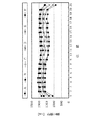
図24は、直径方向に1ポイントから21ポイントまで分割したウェーハの各ポイントにおける図23と同様の結果を示したものである。
通電量および通電時間は、第2実施例と同様であり、2.2Aの電流を30秒間通電するのを複数回繰り返した場合のそれぞれの時点における除去後のCu膜の膜厚を測定したものである。
用いたウェーハおよび電解液の種類などの他の条件は、第2実施例と同様である。
【0150】
図24において、横軸の1ポイントから21ポイントまでは、上述したウェーハにおける位置を示しており、縦軸には除去後の銅の膜厚(nm)を示している。
2.2Aの電流をそれぞれ、Aは0秒間(通電前)、Bは30秒間、Cはトータルで60秒間、Dはトータルで90秒間、Eはトータルで120秒間、Fはトータルで150秒間通電したときのそれぞれの位置における除去後の銅の膜厚を示している。
【0151】
本実施例によれば、各ポイントにおける銅膜の膜厚は、ほぼ電流と時間の積に比例して、減少している。なお、1ポイントと21ポイントの銅膜の膜厚が小さいのは、前段階であるCu膜生成の際のメッキの特性からくるものであり、本発明の研磨方法には無関係である。
【0152】
【発明の効果】
本発明によれば、機械研磨と電解研磨との複合作用によって金属膜を研磨するので、機械研磨による金属膜の平坦化の場合に比べて、非常に高能率に金属膜の凸部の選択的除去および平坦化が可能となる。また、本発明によれば、低い研磨圧力でも十分な研磨レートが得られるため、研磨した金属膜にスクラッチ、ディッシング、エロージョン等が発生するのを抑制することができる。また、金属膜下層の絶縁膜へのダメージを抑制できることから、半導体装置の低消費電力化および高速化等の観点から誘電率を低減するために層間絶縁膜として機械的強度が比較的低い有機系低誘電率膜や多孔質低誘電率絶縁膜を使用した場合にも、容易に適用可能である。さらに、本発明によれば、電解電流をモニタリングすることで、研磨プロセスの管理を行うことができ、研磨プロセスの進行状態を正確に把握することが可能となる。
【図面の簡単な説明】
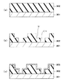
【図1】 図1は、本発明の半導体装置の製造方法の製造工程を示す断面図であり、(a)は半導体基板への絶縁膜形成工程まで、(b)はコンタクトホールおよび配線用溝の形成工程まで、(c)はバリヤ膜の形成工程までを示す。
【図2】 図2は、図1の続きの工程を示し、(d)はシード膜としての銅膜の形成工程まで、(e)は銅膜の形成工程までを示す。
【図3】 図3は、図2の続きの工程を示し、(f)は銅膜の陽極酸化の工程まで、(g)はキレート膜の形成工程までを示す。
【図4】 図4は、図3の続きの工程を示し、(h)は凸部のキレート膜の除去工程まで、(i)はキレート膜の再形成工程までを示す。
【図5】 図5は、図4の続きの工程を示し、(j)は銅膜の平坦化工程まで、(k)は余分な銅膜の除去工程まで、(l)はバリヤ膜の露出工程までを示す。
【図6】 図6は、本実施形態に係る研磨装置の構成を表す図である。
【図7】 図7は、本実施形態に係る研磨装置の研磨工具保持部の内部構造を表す拡大図である。
【図8】 図8(a)は、本実施形態に係る研磨装置に用いる電極板の底面図であり、(b)は電極板付近の拡大図である。
【図9】 図9は、研磨工具とウェーハとの位置関係を示す図である。
【図10】 図10は、本発明に係る研磨装置の電解研磨を説明するための断面図である
【図11】 図11は、図10の円Cにおける拡大断面図である。
【図12】 図12は、図11の円Dにおける拡大断面図である。
【図13】 図13は、本発明の係る研磨装置の第1変形例を示す図である。
【図14】 図14は、本発明に係る研磨装置の第2変形例を示す図である。
【図15】 図15は、本発明に係る研磨装置の従来型CMP装置に応用した第3変形例を示す図である。
【図16】 図16は、図15に示した研磨装置による電解複合研磨動作を説明するための図である。
【図17】 図17は、研磨パッドの電極構成の他の例を示す図である。
【図18】 図18は、研磨パッドの電極構成のさらに他の例を示す図である。
【図19】 図19は、本発明の参考実施形態に係る研磨装置の概略構成図である。
【図20】 図20は、本発明の第2実施形態に係る研磨装置の概略構成図である。
【図21】 図21は、本発明の第3実施形態に係る研磨装置の要部構成図である。
【図22】 図22は、本発明の第1実施例を説明するための図である。
【図23】 図23は、本発明の第2実施例を説明するための図である。
【図24】 図24は、本発明の第3実施例を説明するための図である。
【図25】 図25は、従来例に係るデュアルダマシン法による銅配線の形成方法の製造工程を示す断面図であり、(a)は層間絶縁膜の形成工程まで、(b)は配線用溝およびコンタクトホールの形成工程まで、(c)はバリヤ膜の形成工程までを示す。
【図26】 図26は、図24の続きの工程を示し、(d)はシード膜の形成工程まで、(e)は配線用層の形成工程まで、(f)は配線形成工程までを示す。
【図27】 図27は、CMP法による銅膜研磨工程において発生するディッシングを説明するための断面図である。
【図28】 図28は、CMP法による銅膜研磨工程において発生するエロージョンを説明するための断面図である。
【図29】 図29は、CMP法による銅膜研磨工程において発生するリセスを説明するための断面図である。
【図30】 図30は、CMP法による銅膜研磨工程において発生するスクラッチおよびケミカルダメージを説明するための断面図である。
【符号の説明】
10…研磨工具保持部、11,311,411…研磨工具、12…フランジ部材、13…保持装置、13a…主軸、14…主軸モータ、15…シリンダ装置、15a…ピストン、15b…ピストンロッド、16,316,416…ロータリジョイント、20…通電軸、20a…供給ノズル、21…押圧部材、22…絶縁板、23…電極板、24…スクラブ部材、24a…ワイピング部材、25…弾性部材、26…連結部材、27…通電ブラシ、28…通電部材、30…Z軸位置決め機構部、31…Z軸サーボモータ、31a…ボールネジ軸、32…Z軸スライダ、33…ガイドレール、40…X軸移動機構部、42,342,442…ウェーハテーブル、44…駆動モータ、45…保持装置、46…ベルト、47…加工パン、48…X軸スライダ、49…X軸サーボモータ、51…Z軸ドライバ、52…主軸ドライバ、53…テーブルドライバ、54…X軸ドライバ、55,555,655…コントローラ、56,556,656…コントロールパネル、61,561,661…電解電源、62,562,662…電流計、63…抵抗計、71…スラリー供給装置、81…電解液供給装置、101…半導体基板、102…層間絶縁膜、103…バリヤ膜、104…シード膜、105…銅膜、106…キレート膜、120…陰極部材、201…定盤、202,221,241…研磨パッド、203,223,243…陰極電極、204…陽極電極、206,224,244…絶縁体、207…ウェーハチャック、208…電解液・スラリー供給部、210…銅膜、410…リテーナリング、501,601…水槽、510,610…電極板、520…ジェットポンプ、521,522…管、531,631…第1保持部材、532,632…第2保持部材、533…Z軸位置決め機構、634…第3保持部材、640…パルスジェネレータ、641…アンプ、643…加振器、644…第4保持部材、710…通電ブラシ、SC…スクラッチ、CD…ケミカルダメージ、EL…電解液、SL…スラリー。[0001]
BACKGROUND OF THE INVENTION
The present invention relates to a polishing apparatus, and more particularly, to a polishing apparatus used to relieve uneven surfaces associated with metal film formation.
[0002]
[Prior art]
Along with the high integration and miniaturization of semiconductor devices, the miniaturization of wiring, the reduction of wiring pitch, and the multilayering of wiring are progressing, and the importance of multilayer wiring technology in the manufacturing process of semiconductor devices is increasing.
On the other hand, aluminum has been widely used as a wiring material of a semiconductor device having a multilayer wiring structure. However, in order to suppress a signal propagation delay in a recent design rule of 0.25 μm rule or less, the wiring material is changed from aluminum to copper. The development of a wiring process that replaces is actively conducted. When copper is used for the wiring, there is an advantage that both low resistance and high electromigration resistance can be achieved.
[0003]
In the process of using copper for wiring, for example, a metal is embedded in a groove-shaped wiring pattern formed in advance in an interlayer insulating film, and the excess metal film is removed by CMP (Chemical Mechanical Polishing) method. The wiring process called the damascen method that is formed is influential. This damascene method does not require wiring etching, and has an advantage that the process can be simplified because the upper interlayer insulating film is naturally flat.
In addition, the dual damascene method, in which not only wiring grooves but also contact holes are formed in the interlayer insulating film as grooves and the wiring grooves and contact holes are simultaneously filled with metal, can further reduce the wiring process. Become.
[0004]
Here, an example of the copper wiring forming process by the dual damascene method will be described with reference to the following drawings.
First, as shown in FIG. 25A, for example, an
[0005]
Next, as shown in FIG. 25B, a contact hole CH communicating with the impurity diffusion region of the
[0006]
Next, as shown in FIG. 25C, a
[0007]
Next, as shown in FIG. 26D, copper is deposited with a predetermined film thickness on the
Next, as shown in FIG. 26E, a
[0008]
Next, as shown in FIG. 26F, the
Through the above steps, the
By repeating the above process on the
[0009]
[Problems to be solved by the invention]
However, in the copper wiring formation process using the dual damascene method described above, in the process of removing the
[0010]
In addition, since the removal performance of the
As shown in FIG. 27, for example, when a
As shown in FIG. 28, erosion is a phenomenon in which a portion having a high pattern density, such as a wiring having a width of 1.0 μm formed in a range of 3000 μm at a density of 50%, is excessively removed. If erosion occurs, the cross-sectional area of the wiring is insufficient, which causes a wiring resistance value failure or the like.
As shown in FIG. 29, the recess is a phenomenon in which the
[0011]
On the other hand, in the step of planarizing and removing the
In order to increase the polishing rate, it is necessary to increase the processing pressure on the wafer. When the processing pressure is increased, scratch SC and chemical damage CD are likely to occur on the wiring surface as shown in FIG. It is likely to occur with soft copper. For this reason, it becomes a cause of problems such as wiring open, short, wiring resistance value failure, etc. Also, if the processing pressure is increased, the amount of scratches, interlayer insulation film peeling, dishing, erosion and recesses will increase. There was a disadvantage.
[0012]
The present invention has been made in view of the above-mentioned problems. Therefore, the present invention can easily flatten the initial unevenness when the metal film is flattened by polishing, and can remove excess metal film. An object of the present invention is to provide a polishing apparatus that is excellent in resistance and can suppress damage to a metal film.
[0013]
[Means for Solving the Problems]
In order to achieve the above object, a polishing apparatus of the present invention is a polishing apparatus for polishing an object to be polished having a copper film on a surface to be polished, the conductive polishing tool having a polishing surface, and the polishing tool. A polishing tool rotating and holding means for rotating and holding a workpiece about a predetermined rotation axis, and holding and rotating the object to be polished about a predetermined rotating shaft.CoveredA polishing object rotating and holding means, a movement positioning means for moving and positioning the polishing tool in a direction substantially perpendicular to the surface to be polished of the object to be polished, and a surface to be polished and a surface to be polished are predetermined. Relative movement means for relatively moving along a plane, electrolyte supply means for supplying an electrolyte containing a chelating agent on the surface to be polished, the surface to be polished as an anode and the polishing tool as a cathode, and the object to be polished Current supply means for supplying a current flowing from the surface to the polishing tool through the electrolytic solution;The current supply means is arranged so as to be in contact with or close to the surface to be polished, and applies a predetermined voltage between the anode member and the polishing tool, the anode member energizing with the surface to be polished as an anode The polishing tool has an annular shape, one end surface of the ring constitutes a polishing surface, the anode member is provided in a non-contact manner inside the ring of the polishing tool, It is rotated and held together with the polishing tool by the polishing tool rotation holding means..
[0014]
According to the above polishing apparatus of the present invention, for example, when a copper film having irregularities is formed on the surface to be polished, the surface of the copper film to be polished is anodized by the current supply means. Then, the anodized copper is chelated by the chelating agent in the electrolytic solution supplied by the electrolytic solution supplying means, and a chelate film having a very low mechanical strength that can be easily removed is formed.
By moving or positioning the polishing surface in contact with or approaching the surface to be polished, and rotating the polishing surface and the surface to be polished in contact with or in proximity to each other by the polishing tool rotation holding unit and rotation holding unit, respectively. The convex portion is removed, and further, the convex portion of the chelate film on the entire surface to be polished is polished and removed by the relative movement means, whereby the object to be polished can be efficiently polished with a low polishing pressure.
[0015]
Also,Stable current supply can be performed by flowing current locally through the electrolytic solution through the electrolytic solution by the anode member. In this case, the surface to be polished is energized from the anode member through the electrolytic solution, and further from the surface to be polished to the polishing tool through the electrolytic solution, so that the copper film in the vicinity of the polishing tool as the cathode is anodized. And chelated.
[0016]
In the polishing apparatus of the present invention, preferably, the power source outputs a pulsed voltage having a predetermined cycle.
For example, by making the pulse width very short, the amount of chelate film produced by anodization per pulse is very small, and discharge due to a sudden change in the distance between electrodes, such as contact with surface irregularities, bubbles, particles, etc. It is effective to prevent sudden and enormous anodic oxidation of the copper film, such as spark discharge caused by a sudden change in electric resistance that occurs when the intervening metal is interposed, and to make as small as possible continuous.
[0017]
In the polishing apparatus of the present invention, preferably, the anode member is made of a noble metal as compared with copper formed on the surface to be polished. Thereby, elution to the electrolyte solution of an anode member, etc. can be prevented, and a copper film can be actively anodized. In addition, since the cathode does not elute originally, it is not necessary to consider nobility.
[0018]
In the polishing apparatus of the present invention, preferably, the current detection unit detects a value of a current flowing from the surface to be polished to the polishing tool, and the current value is constant based on a detection signal from the current detection unit. And a control means for controlling the position of the polishing tool in a direction substantially perpendicular to the surface to be polished.
By controlling the current value to be constant, the current density is always constant, and the amount of chelate film produced by anodic oxidation can also be controlled to be constant.
[0021]
Furthermore, in order to achieve the above object, the polishing apparatus of the present invention is arranged in parallel with the holding means for holding the object to be polished and the surface to be polished.RuElectrode plate and the object to be polishedConsists of connected pulse generator, amplifier and vibratorVibration means;Does not contain abrasive grains,Electrolyte containing chelating agentWhen,A water tank for storing the electrolyte solution;An electrolytic current supply means for supplying an electrolytic current flowing from the polished surface to the electrode plate through the electrolytic solution using the polished surface as an anode and the electrode plate as a cathode;The electrolytic current supply means outputs a pulsed voltage every 20 to 50 msec, the holding means for the object to be polished and the electrode plate are disposed so as to be immersed in the electrolytic solution, and the copper film The electrolysis current supply means supplies the electrolysis current so that the chelating agent forms a chelate film by reacting with the chelating agent, and the vibration excitation means removes the convex portion of the chelate film. It vibrates the object.
[0022]
According to the above polishing apparatus of the present invention, for example, when an uneven copper film is formed on the surface to be polished of the object to be polished, the surface of the copper film of the surface to be polished is The oxidized and anodized copper is chelated by the chelating agent in the electrolytic solution supplied by the electrolytic solution supply means, and a chelate film having a very low mechanical strength that can be easily removed is formed.
The convex portion of the chelate film is selectively removed by the vibration action on the object to be polished by the vibration means, and efficient polishing with little damage to the object to be polished can be achieved.
[0025]
Furthermore, in order to achieve the above object, a polishing apparatus of the present invention is a polishing apparatus for polishing an object to be polished having a metal film on a surface to be polished, the object to be polishedThe surface to be polishedDispel, Vents were providedWaiPing member and,A counter electrode disposed on an upper surface of the wiping member, facing the surface to be polished, and a wiping member rotation holding unit that rotates and holds the counter electrode and the wiping member around a predetermined rotation axis; The object to be polished rotating and holding means for holding the object to be polished and rotating around a predetermined rotation axis;Polishing targetOn the surfaceElectrolyte supply means for supplying an electrolyte, and the object to be polishedsurfaceCurrent supply means for supplying current between the counter electrodes;The wiping member rotating and holding means and having a through hole connected perpendicularly to the center of the counter electrode and the wiping member and having a current-carrying shaft through which the current is passed. The electrolytic solution is supplied onto the surface to be polished from the electrolytic solution supply unit through the through hole, through the wiping member..
[0026]
Furthermore, in order to achieve the above object, the polishing apparatus of the present invention comprises:in frontPolishingsurfaceAnd said WaiPing member andRelative movement means for relative movementFurtherHave.
[0027]
The relative moving means isin frontPolishingsurfaceTo the WaiPing memberPress the said polishedsurfaceAbove WaiPing memberMove horizontally. Alternatively, the relative movement means may be the YPing memberofOn the polished surface sideOn the surfaceSo that the surface to be polished is locatedThe object to be polishedrotationThe holding means is moved horizontally.
[0028]
According to the polishing apparatus of the present invention, for example, when a metal film is formed on the surface to be polished, the electrolytic solution is supplied onto the surface of the object to be polished by the electrolytic solution supply means, By supplying a current between the surface of the object to be polished and the counter electrode by the current supply means, the metal film on the surface to be polished is anodized and becomes an ionic state, and the mechanical strength that can be easily removed is very low. It becomes a state.
Then, by wiping the surface of the anodized metal film with a wiper, the anodized metal film is removed, so that the object to be polished can be efficiently polished with a low pressure.
[0029]
DETAILED DESCRIPTION OF THE INVENTION
Embodiments of the present invention will be described below with reference to the drawings.
[0030]
First embodiment
(Manufacturing method and polishing method of semiconductor device)
As an example, a case where the embodiment of the present invention is applied to a metal wiring forming process by a dual damascene method in a semiconductor device manufacturing process will be described.
[0031]
First, as shown in FIG. 1A, an
As the
Here, examples of the low dielectric constant insulating film include SiF, SiOCH, polyaryl ether, porous silica, and polyimide.
[0032]
Next, as shown in FIG. 1B, a contact hole CH and a wiring groove M leading to the impurity diffusion region of the
[0033]
Next, as shown in FIG. 1C, a
The
The
[0034]
Next, as shown in FIG. 2D, a
[0035]
Next, as shown in FIG. 2E, the
On the surface of the
In the following, for example, a case where copper is laminated as a wiring layer will be described.
[0036]
The above process is performed in the same manner as in the prior art. However, in the polishing method of the present invention, the removal of the
[0037]
As shown in FIG. 3 (f), the chelate film is formed by disposing the electrolyte member EL in which the
In addition to the above, the electrolytic solution EL can contain a brightener, Cu ions, and the like as additives.
The temperature of the electrolytic solution is controlled to optimize the oxidation of the metal film surface, the chelate formation ratio, the wiping ratio, and the like.
Here, as the chelating agent, for example, quinaldic acid of chemical structural formula (1), glycine of chemical structural formula (2), citric acid of chemical structural formula (3), oxalic acid of chemical structural formula (4), chemical A propionic acid having the structural formula (5) or the like is used.
Next, a voltage is applied using the
[0038]
[Chemical 1]
[Chemical formula 2]
NH2 CH2 COOH (2)
[0040]
[Chemical 3]
[Formula 4]
(COOH)2 (4)
[0042]
[Chemical formula 5]
C2 HFive COOH (5)
[0043]
The
[0044]
As shown in FIG. 3G, the surface of the anodized copper film (CuO) 105 is chelated by a chelating agent in the electrolytic solution. When quinaldic acid is used as the chelating agent, the film is made of a chelate compound of chemical structural formula (6), and when glycine is used, the film is made of a chelate compound of chemical structural formula (7). These
[0045]
[Chemical 6]
[Chemical 7]
Next, as shown in FIG. 4H, the convex portions of the
At this time, since the convex portion of the
[0048]
Next, as shown in FIG. 4 (i), the convex portion of the
Thereafter, the convex portion of the
[0049]
Next, as shown in FIG. 5J, the
[0050]
Next, as shown in FIG. 5 (k), the process of removing the generated chelate film by anodic oxidation is continued on the entire surface of the flattened
[0051]
Next, as shown in FIG. 5L, the entire surface of the
Thereafter, the copper film is formed by removing the
[0052]
According to the polishing method according to the present embodiment, the polishing is performed with the polishing rate being assisted electrochemically, and therefore, polishing can be performed at a lower processing pressure compared to normal chemical mechanical polishing. This is very advantageous in terms of reduction of scratches, step relief performance, reduction of dishing and erosion, as compared with simple mechanical polishing.
Further, since the polishing can be performed at a low processing pressure, an organic low dielectric constant film or a porous low dielectric constant insulating film which is weak in mechanical strength and easily broken by a normal chemical mechanical polishing is used as the
[0053]
When slurry containing alumina particles or the like is used in normal chemical mechanical polishing, it contributes to CMP processing and remains without being worn out or buried in the copper surface (particles). In the polishing method, even when mechanical polishing or wiping using a chelating agent that does not contain abrasive grains as an electrolyte, the chelate film formed on the surface has a very low mechanical strength and can be sufficiently removed.
Further, by monitoring the electrolytic current, the polishing process can be managed, and the progress of the polishing process can be accurately grasped.
[0054]
The polishing method according to the present invention is not limited to the above embodiment.
In addition to copper, as described above, for example, it can be applied to a wiring layer made of Al, W, WN, Cu, Au, Ag or the like or an alloy film thereof, and polishing of a barrier film made of the above-described materials or the like. It can also be applied to.
Further, the present invention can be applied to polishing various metal films used other than wirings.
Various modifications such as the type of chelating agent and the type of the cathode member can be made without departing from the gist of the present invention.
Further, the method for manufacturing a semiconductor device according to the present invention is not limited to the above embodiment.
For example, the method other than the metal film polishing method is not limited in any way, and in the present embodiment, the dual damascene method has been described as an example, but the present invention can also be applied to the single damascene method. Various changes can be made to the forming method, the forming method of the copper film, the forming method of the barrier film and the like without departing from the gist of the present invention.
[0055]
(Polishing equipment)
FIG. 6 is a diagram showing the configuration of the polishing apparatus according to the embodiment of the present invention.
The polishing apparatus shown in FIG. 6 includes a processing head unit, an
Although not shown, the polishing apparatus is installed in a clean room, and in the clean room, a loading / unloading port for loading / unloading a wafer cassette storing a wafer to be polished is provided. Further, a wafer transfer robot for transferring wafers between the wafer cassette carried into the clean room through the carry-in / out port and the polishing apparatus is installed between the carry-in / out port and the polishing apparatus. Moreover, the cleaning mechanism for cleaning the wafer after being polished by the polishing apparatus may be configured as one unit.
[0056]
The processing head unit holds the polishing
[0057]
The Z-
[0058]
The Z-
With the above configuration, the ball screw shaft 31a is rotated by driving the Z-
[0059]
The X-axis moving
[0060]
The wafer table 42 sucks the wafer W by, for example, vacuum suction means.
The
The
The
[0061]
The
[0062]
The electrolytic
As the electrolyte, one based on an organic solvent or an aqueous solution can be used.
Examples of the acid in the electrolyte include copper sulfate, ammonium sulfate, and phosphoric acid. Examples of the alkali include ethyldiamine, NaOH, and KOH.
Moreover, organic solvent dilution liquid mixture, such as methanol, ethanol, glycerol, ethylene glycol, can also be used as electrolyte.
Additives include Cu ions, brighteners or chelating agents.
As the brightener, for example, sulfur, copper ion such as copper hydroxide and copper phosphate, chlorine ion such as hydrochloric acid, benzotriazole (BTA), polyethylene glycol and the like can be used.
As the chelating agent, for example, quinoline, anthranilic acid and the like are used in addition to the above-described quinaldic acid, glycine, citric acid, oxalic acid, propionic acid and the like.
[0063]
FIG. 7 is a diagram illustrating an internal structure of the polishing
The polishing
[0064]
The
The
[0065]
The holding
[0066]
The
Since the
An
[0067]
The
A
A pressing
The pressing
[0068]
A through hole is formed at the center of the
The energizing
[0069]
The energizing
The energizing
[0070]
The rotary joint 16 is electrically connected to the positive electrode of the
[0071]
The electrode plate (anode member) 23 connected to the lower end portion of the current-carrying
The upper surface side of the
[0072]
The insulating
In addition, the insulating
[0073]
By making the insulating
When the supply of high-pressure air to the
[0074]
The polishing
The polishing
That is, the conductive energizing
[0075]
The electrolytic power source (current supply means) 61 is a device that applies a predetermined voltage between the rotary joint 16 and the energizing member (cathode energizing member) 28 described above. By applying a voltage between the rotary joint 16 and the energizing
The
Specifically, a power source that outputs a pulsed voltage at a constant period and can change the pulse width as appropriate is used. As an example, the output voltage is 2 to 5 V DC, the maximum output current is 2 to 3 A, and the pulse width can be changed to any one of 1, 2, 5, 10, 20, and 50 msec.
The reason why the pulse-like voltage output is short as described above is to make the amount of anodic oxidation per pulse very small. That is, a spark caused by a sudden change in the distance between the electrodes, such as contact with the unevenness of a metal film such as copper formed on the surface of the wafer W, or a spark caused by a sudden change in electrical resistance caused by bubbles or particles. This is effective in preventing sudden and enormous anodic oxidation of the metal film, such as electric discharge, and making it as small as possible.
In addition, since the output voltage is relatively high compared to the output current, a certain margin can be set for setting the distance between the electrodes. That is, even if the distance between the electrodes changes slightly, the change in current value is small because the output voltage is high.
The pulse to be applied is not limited to the above, and a rectangular pulse, a sine waveform, a sawtooth waveform, or a PAM waveform may be applied as a periodic pulse.
[0076]
The
Further, the
[0077]
The
In addition, the
[0078]
The
The
It is possible to apply a periodic pulse set so that the current flowing through the cathode member and the metal film changes stepwise. For example, in the initial stage of removing the metal film, the current flowing through the cathode member and the metal film is A periodic pulse set so as to increase gradually is applied. As a result, it is possible to prevent the surface state of the metal film to be removed from being deteriorated by instantaneously applying a high voltage at the start of voltage application.
Further, since the current value signal 62s becomes small near the end point of the metal film removal, when the current value signal 62s becomes smaller than the predetermined threshold value compared to the predetermined threshold value, the vicinity of the end point is reached. As a result, the output pulse is controlled to be small, and then a control signal is output to the
[0079]
The
[0080]
Here, FIG. 8A is a bottom view showing an example of the structure of the
As shown in FIG. 8A, a circular opening (supply nozzle) 23a is provided at the center of the
Further, as shown in FIG. 8B, the lower end portion of the energizing
[0081]
With such a configuration, the slurry and the electrolyte supplied through the
That is, when the slurry and the electrolyte are supplied to the upper surface of the
The
[0082]
The
[0083]
FIG. 9 shows the positional relationship between the polishing
The central axis of the polishing
[0084]
Thus, when the central axis of the polishing
In the polishing apparatus according to the present embodiment, a part of the polishing
Thereby, if the value of the electrolysis current is controlled to be constant, the current density can always be constant, and the amount of chelation by anodic oxidation of the metal film can always be constant.
[0085]
Next, the polishing operation (polishing method) by the above-described polishing apparatus will be described by taking as an example a case where a copper film is polished as a metal film formed on the surface of the wafer W, for example. FIG. 10 is a schematic view showing a state in which the
First, the wafer W is chucked on the wafer table 42, and the wafer table 42 is driven to rotate the wafer W at a predetermined number of rotations.
Further, the wafer table 42 is moved in the X-axis direction, the polishing
[0086]
In this state, when the slurry SL and the electrolyte EL are supplied from the
The polishing
In addition, the
[0087]
Further, high pressure air is supplied to the
From this state, the wafer table 42 is moved in the X-axis direction with a predetermined speed pattern, and the entire surface of the wafer W is polished uniformly.
[0088]
11 is an enlarged view in a circle C in FIG. 10, and FIG. 12 is an enlarged view in a circle D in FIG.
As shown in FIG. 11, the
As shown in FIG. 11, the insulating
[0089]
For this reason, the current i that flows from the
The current i is applied to the surface of the copper film MT.2 , The copper constituting the copper film MT is anodized by the electrolytic action of the electrolytic solution EL and chelated by the chelating agent in the electrolytic solution.
[0090]
Here, the resistance R1 in the electrolyte EL becomes extremely large in proportion to the distance d between the
Also, the current i2 Is the gap δb And gap δw As described above, the position of the polishing
Further, the positioning accuracy of the polishing apparatus in the Z-axis direction is sufficiently high with a resolution of 0.1 μm. In addition, the effective contact area is obtained by inclining the
[0091]
As described above, the polishing apparatus having the above configuration has an electrolytic polishing function for generating and removing a chelate film by anodization on the surface of the copper film MT formed on the wafer W described above.
Further, in addition to the electrolytic polishing function, the polishing apparatus having the above configuration also has a chemical mechanical polishing function of a normal CMP apparatus using the
Moreover, the polishing apparatus having the above-described configuration can also perform polishing by a combined action of mechanical polishing of the polishing
[0092]
According to the polishing apparatus according to the present embodiment, a metal film such as copper can be polished by the combined action of electrolytic polishing and chemical mechanical polishing, which is far more than a polishing apparatus using only chemical mechanical polishing or only mechanical polishing. In addition, the metal film can be removed with high efficiency. Since a high polishing rate for the metal film can be obtained, the processing pressure F for the wafer W of the polishing
[0093]
In addition, when a slurry containing alumina particles or the like is used in a slurry used for normal chemical mechanical polishing, the slurry may remain on the metal film surface or be buried after polishing without being worn. In the polishing apparatus according to the embodiment, even when only mechanical polishing using an electrolytic solution containing a chelating agent that does not contain abrasive grains, the chelate film remaining on the surface is very low in mechanical strength and can be removed sufficiently. Therefore, it is possible to prevent particles and slurry from remaining on the wafer surface.
[0094]
Further, the positioning accuracy in the Z-axis direction of the polishing apparatus is sufficiently high as a resolution of 0.1 μm. In addition, the effective contact area is obtained by inclining the
In the embodiment described above, the absolute value of the polishing amount of the metal film can be controlled by the integrated amount of the electrolytic current and the time for passing the wafer W of the polishing
[0095]
FIG. 13 is a schematic view showing a modification of the polishing apparatus according to the present invention.
In the polishing apparatus according to the above-described embodiment, the surface of the wafer W is energized by the
As shown in FIG. 13, the wheel-
In this case, energization of the wafer table 342 is performed by providing a rotary joint 316 below the wafer table 342 so that the energization of the wafer table 342 rotated by the rotary joint 316 is always maintained. Supply can be made.
[0096]
FIG. 14 is a schematic view showing another modification of the polishing apparatus according to the present invention.
A wafer table 442 for chucking and rotating the wafer W holds the wafer W by a
The
In addition, the
Even when the
[0097]
FIG. 15 is a schematic configuration diagram showing another embodiment of the polishing apparatus according to the present invention.
The polishing apparatus shown in FIG. 15 is obtained by adding the electrolytic polishing function of the present invention to a conventional CMP apparatus, and is a polishing surface of a polishing tool in which a polishing pad (polishing cloth) 202 is bonded on a
[0098]
On the
The
Further, this polishing apparatus is provided with a
[0099]
Here, FIG. 16 is a diagram for explaining an electrolytic composite polishing operation (polishing method) by the polishing apparatus having the above-described configuration. It is assumed that a
As shown in FIG. 16, during electrolytic composite polishing, the anode EL is in a state where an electrolytic solution EL and a slurry SL are interposed between the
At this time, in the vicinity of the circle G shown in FIG. 16, the surface of the
[0100]
By adopting such a configuration, the same effects as those of the polishing apparatus according to the above-described embodiment can be obtained.
The arrangement of the anode electrode and the cathode electrode provided on the polishing pad is not limited to the configuration shown in FIG. 15. For example, as shown in FIG. 17, a plurality of
Further, for example, as shown in FIG. 18,
[0101]
Reference embodiment
FIG. 19 illustrates the present invention.reference1 is a schematic configuration diagram of a polishing apparatus according to an embodiment. The polishing apparatus according to this embodiment includes a
[0102]
The holding means 530 is fixed to a conductive first holding
[0103]
The
[0104]
As the electrolytic solution EL, the same one as in the first embodiment can be used. For example, the electrolytic solution EL includes a chelating agent that chelates a metal such as copper, and may include other additives. For example, copper sulfate is used as the electrolyte to reduce the voltage applied between the wafer and the
[0105]
The electrolytic power supply (electrolytic current supply means) 561 is preferably not a constant voltage power supply that always outputs a constant voltage, but preferably a power supply that outputs the voltage in pulses at a constant cycle. For example, the voltage applied by the
[0106]
As the pulse voltage, a voltage and a pulse width that can remove metal most efficiently can be selected according to the distance d between the wafer and the
If the distance d between the
[0107]
The
In addition, the
[0108]
A
[0109]
Also by the configuration of the above polishing apparatus, as in the polishing apparatus according to the first embodiment, for example, when a metal film having irregularities is formed on the surface of the wafer W, by applying the wafer W as an anode, Since the metal film surface of the wafer W is anodized and the anodized metal film is chelated by the chelating agent in the electrolyte EL, and the chelate has very low mechanical strength, the
Further, by monitoring the electrolytic current, the polishing process can be managed, and the progress of the polishing process can be accurately grasped.
[0110]
According to the polishing apparatus of this embodiment, the removal of the metal film can be achieved by removing the chelate film having a very low mechanical strength. Therefore, the conventional polishing apparatus using only chemical mechanical polishing or only mechanical polishing. Compared with this, the metal film can be removed much more efficiently.
Since strong pressing as in conventional mechanical polishing is not required, damage to the interlayer insulating film under the wiring metal film can be kept low, and the occurrence of dishing, erosion, and the like can be suppressed. Since a high pressure is not applied to the insulating film under the wiring metal film, the insulating film material can be applied to a low dielectric constant material whose mechanical strength is lower than that of silicon oxide using TEOS or the like as a raw material.
Moreover, since the apparatus configuration is simple as a polishing apparatus, it is possible to easily realize downsizing, easy maintenance, and improvement in operating rate.
[0111]
Furthermore, in a slurry used for normal chemical mechanical polishing, when a slurry containing alumina particles or the like is used, the slurry does not wear out after polishing and may remain on the metal surface or be buried. Such a polishing apparatus does not have such a problem.
[0112]
The present invention is not limited to the above embodiment. For example, various modifications are possible without departing from the scope of the present invention, such as the configuration of the jet pump, the type of electrode plate, and the configuration of the apparatus for holding the wafer in the water tank.
[0113]
Second embodiment
FIG. 20 shows the first aspect of the present invention.21 is a schematic configuration diagram of a polishing apparatus according to an embodiment. In the polishing apparatus according to the present embodiment, a vibration unit including a
[0114]
The holding means 630 includes a first holding
[0115]
The
[0116]
As the electrolytic solution EL, the same one as in the first embodiment can be used. For example, the electrolytic solution EL includes a chelating agent that chelates a metal such as copper, and may include other additives. For example, copper sulfate is used as the electrolyte to reduce the voltage applied between the wafer and the
[0117]
The
[0118]
The electrolytic power source (electrolytic current supply means) 661 is preferably a power source that outputs a voltage in a pulse form at a constant cycle, instead of a constant voltage power source that always outputs a constant voltage. For example, the voltage applied by the
[0119]
As the pulse voltage, a voltage and a pulse width that can most efficiently remove the metal film can be selected depending on the distance d between the wafer and the
If the distance d between the
[0120]
The
[0121]
A
[0122]
Also by the configuration of the above polishing apparatus, as in the polishing apparatus according to the first embodiment, for example, when a metal film having irregularities is formed on the surface of the wafer W, by applying the wafer W as an anode, Since the metal film surface of the wafer W is anodized, the anodized metal film is chelated by the chelating agent in the electrolyte EL, and the chelate has a very low mechanical strength. By removing the convex portions of the chelate film by the wafer vibrating means, the metal film can be planarized and removed.
Further, by monitoring the electrolytic current, the polishing process can be managed, and the progress of the polishing process can be accurately grasped.
[0123]
According to the polishing apparatus of this embodiment, the removal of the metal film can be achieved by removing the chelate film having a very low mechanical strength. Therefore, the conventional polishing apparatus using only chemical mechanical polishing or only mechanical polishing. Compared with this, the metal film can be removed much more efficiently.
Since strong pressing as in conventional mechanical polishing is not required, damage to the interlayer insulating film under the wiring metal film can be kept low, and the occurrence of dishing, erosion, and the like can be suppressed. Since a high pressure is not applied to the insulating film under the wiring metal film, the insulating film material can be applied to a low dielectric constant material whose mechanical strength is lower than that of silicon oxide using TEOS or the like as a raw material.
Moreover, since the apparatus configuration is simple as a polishing apparatus, it is possible to easily realize downsizing, easy maintenance, and improvement in operating rate.
[0124]
Furthermore, in a slurry used for normal chemical mechanical polishing, when a slurry containing alumina particles or the like is used, the slurry does not wear out after polishing and may remain on the metal surface or be buried. Such a polishing apparatus does not have such a problem.
[0125]
The present invention is not limited to the above embodiment. For example, various modifications can be made without departing from the scope of the present invention, such as the configuration of the vibrator and the amplifier, the type of the electrode plate, and the configuration of the apparatus for holding the wafer in the water tank.
[0126]
Third embodiment
FIG. 21 shows a configuration diagram of a main part of the polishing apparatus according to the present embodiment. The basic configuration is the same as that of the first embodiment, but in this embodiment, the metal film on the wafer is removed by the wiping
[0127]
The wiping
The above material needs to be a material that is not affected by the electrolytic solution EL.
Further, since the wiping
For example, the pressure for wiping only the convex portion of the metal film on the wafer surface W is about 20 to 100 g / cm.2 In addition, it is necessary to have a hardness that can withstand elasticity even in the case of, and has a softness that does not cause scratches or scratches.
[0128]
As a material that satisfies the above conditions, an elastoplastic material can be used, for example, polyvinyl acetal (PVA), foamed urethane, Teflon foamed body, Teflon fiber nonwoven fabric, or the like.
Further, it may have conductivity, and a relatively soft material such as carbon having a conductive binder matrix (binder) itself, or a conductive material such as sintered copper, metal compound, etc. A porous body made of a resin such as urethane resin, melamine resin, epoxy resin, or polyvinyl acetal (PVA) can also be used.
[0129]
The
Similarly to the first embodiment, the
Further, the
[0130]
As in the first embodiment, the
Here, in this embodiment, the voltage application direction is reversed, and accordingly, the voltage is applied so that the energizing
Specifically, as in the first embodiment, there is no particular limitation as long as it is a power source that outputs a pulsed voltage at a constant cycle and can appropriately change the pulse width. For example, a PR (Periodic Reverse) pulse voltage that repeats plus and minus at a predetermined cycle centering on 0 V is applied. As this PR pulse voltage, for example, a positive voltage with an output voltage of about 0.8 to 1.2 V and a reverse voltage of about −0.8 to −1.2 V are repeated, and the current density is 10 mA / cm.2 Back flow is 10 mA / cm2 The pulse width is about 20 to 50 msec for the forward flow pulse and about 5 to 10 msec for the reverse flow pulse.
Note that the pulse to be applied is not limited to the above, as in the first embodiment.
[0131]
The energizing
[0132]
The operation of the above polishing apparatus will be described.
First, the wafer W is chucked on the wafer table 42, and the wafer table 42 is driven to rotate the wafer W at a predetermined number of rotations.
Further, the wafer table 42 is moved in the X-axis direction, the wiping
[0133]
From this state, when the electrolyte solution EL is supplied from the electrolyte
Further, the
[0134]
As a result, a positive potential is directly applied to the metal film on the wafer surface through the energizing
Therefore, the metal film under the wiping
[0135]
In the above state, high pressure air is supplied to the
From this state, the wafer table 42 is moved in the X-axis direction with a predetermined speed pattern, and the entire surface of the wafer W is wiped uniformly.
[0136]
As described above, the polishing apparatus having the above configuration can generate and remove a chelate film by anodization on the surface of the metal film formed on the wafer W described above.
[0137]
According to the polishing apparatus according to the present embodiment, the same effects as those of the polishing apparatus according to the first embodiment can be obtained.
Furthermore, in the polishing apparatus according to the present embodiment, the level difference of the metal film on the wafer surface can be alleviated only by wiping with the wiping
[0138]
In the present embodiment, an example in which the wiping member is rotated is shown as the wiping method. However, it is only necessary that the wiping member can be moved relative to the wafer W. It is also possible to move it horizontally. In the case of wiping by this horizontal movement, the horizontal movement speed is preferably about 15 m / min or less in order to prevent the electrolyte from scattering.
In order to promote anodic oxidation, the temperature of the electrolytic solution is preferably adjusted to about 80 ° C. or less.
It is also possible to supply an electrolytic solution to the surface of the object to be polished and hold the electrolytic solution with surface tension.
Furthermore, as an example of the object to be polished, there is no particular limitation as described above.
[0139]
The polishing apparatus according to the present invention is not limited to the above-described embodiment. For example, as described above, as an example of an object to be polished, in addition to a copper film, in addition to aluminum, tungsten, gold, silver, and the like, they are widely applied to metal films such as alloys thereof, nitrides and oxides of the alloys, and the like. be able to. Further, these metal films are not limited to uses such as wiring and contacts. In the present embodiment, the first and first3In the embodiment, the wiping
[0140]
【Example】
Embodiments using the polishing apparatus of the present invention will be described below with reference to the drawings.
[0141]
First embodiment
FIG. 22 shows the first of the present invention.2The removal amount per unit time of the copper film when the copper film on the surface of the wafer W is removed by chelation by anodic oxidation using the polishing apparatus according to the embodiment, and the first aspect of the present invention.2In the polishing apparatus according to the embodiment, hydrogen peroxide (H) is used as an oxidizing agent for the copper film on the surface of the wafer W in the electrolyte EL without applying a voltage to the wafer W.2 O2 ) Is added at a predetermined concentration, and the removal amount per unit time of the copper film when the copper film on the surface of the wafer W is removed by chelation by oxidation is compared.
[0142]
In FIG. 22, copper is oxidized by adding an oxidant without applying a voltage, and after chelation, (A) is removed, and a quinaldic acid solution is used as the electrolyte, and H2 O2 The removal amount (removal rate) of the copper film per unit time at concentrations of 0%, 4.5%, 8%, and 10.7% was measured. The amount of the electrolytic solution was 150 ml. In addition, the first of the present invention2The copper film removed using the polishing apparatus according to the embodiment is (B), 150 ml of quinaldic acid solution is used as the electrolytic solution EL, hydrogen peroxide is not included, and the electrolytic solution EL is applied to the
[0143]
When hydrogen peroxide is used as the oxidizing agent, Cu is oxidized to form a copper hydrate ion ([Cu (OH)Four ]2-) Is formed. The copper hydrate ion is chelated by the chelating agent in the electrolyte EL. For example, when the chelating agent is quinaldic acid, a chelate of the chemical structural formula (6) is generated, and when the chelating agent is glycine. A chelate of chemical structural formula (7) is produced.
[0144]
As other experimental conditions, a wafer of 8 inches was used, the barrier metal was Ta with a thickness of 25 nm, the interlayer insulating film was a TEOS (tetraethylorthosilicate) film with a thickness of 1200 nm, and the copper was used. The film thickness was 1600 nm.
[0145]
In FIG. 22, as the amount of hydrogen peroxide as the oxidant increases, the amount of chelate film produced by oxidation of the copper film increases, so the amount of copper film removed per unit time increases. As can be seen, when the polishing method by the polishing apparatus according to the third embodiment of the present invention is used, only the chelate is generated by the anodic oxidation of copper by energization without adding hydrogen peroxide, and it depends on the oxidizing agent. It can be seen that the removal rate is dramatically improved.
[0146]
Second embodiment
FIG. 23 shows a first embodiment of the present invention applied to a wafer W having a copper film on the surface.2Using the polishing apparatus according to the embodiment, with the copper film as an anode, the chelate film was removed every time a current of 2.2 A was passed for 30 seconds, and the film thickness of Cu after the removal of the chelate film was measured. The measurement portion was measured for a 21-point portion when an 8-inch wafer was divided in the diameter direction from 1 point to 21 points. The
[0147]
In FIG. 23, 0, 1, 2, 3, 4, and 5 on the horizontal axis each represent the number of times a current of 2.2 A is applied for 30 seconds. Therefore, the current of 2.2A respectively, 0 is not energized, 1 is 30 seconds, 2 is total 60 seconds, 3 is total 90 seconds, 4 is total 120 seconds, 5 is total 150 seconds Indicates that power was supplied.
The vertical axis indicates the film thickness (nm) of copper remaining on the wafer surface after copper is removed after energization.
In addition, the said measurement was performed in multiple times on the same conditions.
[0148]
From the measurement results, it can be seen that the thickness of the Cu film after removal decreases in proportion to the energization time each time the current is applied for a predetermined time. The average removal amount was 202.68 nm / min.
[0149]
Third embodiment
FIG. 24 shows the same result as FIG. 23 at each point of the wafer divided from 1 point to 21 points in the diameter direction.
The energization amount and energization time were the same as in the second example, and the film thickness of the Cu film after removal at each time point when the current of 2.2 A was energized for 30 seconds was repeated several times. It is.
Other conditions such as the used wafer and the type of electrolytic solution are the same as in the second embodiment.
[0150]
In FIG. 24, points 1 to 21 on the horizontal axis indicate positions on the wafer described above, and the vertical axis indicates the film thickness (nm) of copper after removal.
2.2A current for 0 seconds (before energization), B for 30 seconds, C for a total of 60 seconds, D for a total of 90 seconds, E for a total of 120 seconds, F for a total of 150 seconds The copper film thickness after removal at each position is shown.
[0151]
According to this example, the film thickness of the copper film at each point decreases almost in proportion to the product of current and time. The thin film thicknesses of the 1-point and 21-point copper films come from the plating characteristics when the Cu film was formed in the previous stage, and are irrelevant to the polishing method of the present invention.
[0152]
【The invention's effect】
According to the present invention, since the metal film is polished by the combined action of mechanical polishing and electrolytic polishing, the metal film protrusions can be selectively selected very efficiently compared to the case of flattening the metal film by mechanical polishing. Removal and planarization are possible. Further, according to the present invention, since a sufficient polishing rate can be obtained even at a low polishing pressure, it is possible to suppress the occurrence of scratches, dishing, erosion and the like in the polished metal film. In addition, since the damage to the insulating film under the metal film can be suppressed, an organic system having a relatively low mechanical strength as an interlayer insulating film in order to reduce the dielectric constant from the viewpoint of reducing the power consumption and speeding up of the semiconductor device. Even when a low dielectric constant film or a porous low dielectric constant insulating film is used, it can be easily applied. Furthermore, according to the present invention, the polishing process can be managed by monitoring the electrolytic current, and the progress of the polishing process can be accurately grasped.
[Brief description of the drawings]
FIG. 1 is a cross-sectional view showing a manufacturing process of a method for manufacturing a semiconductor device according to the present invention, where (a) shows an insulating film forming process on a semiconductor substrate, and (b) shows a contact hole and a wiring groove. (C) shows up to the formation process of the barrier film.
FIG. 2 shows a step subsequent to FIG. 1, in which (d) shows a process up to the formation of a copper film as a seed film, and (e) shows a process up to the formation of the copper film.
FIG. 3 shows a process continued from FIG. 2, in which (f) shows a copper film anodizing process and (g) shows a chelate film forming process.
4 shows a process subsequent to FIG. 3, in which (h) shows the process up to the removal of the chelate film on the convex part, and (i) shows up to the process of re-forming the chelate film.
5 shows a continuation process of FIG. 4, in which (j) is up to the copper film flattening process, (k) is up to the removal process of excess copper film, and (l) is the exposure of the barrier film. The process is shown.
FIG. 6 is a diagram illustrating a configuration of a polishing apparatus according to the present embodiment.
FIG. 7 is an enlarged view showing the internal structure of the polishing tool holding part of the polishing apparatus according to the present embodiment.
FIG. 8A is a bottom view of an electrode plate used in the polishing apparatus according to the present embodiment, and FIG. 8B is an enlarged view of the vicinity of the electrode plate.
FIG. 9 is a diagram illustrating a positional relationship between a polishing tool and a wafer.
FIG. 10 is a cross-sectional view for explaining electropolishing of the polishing apparatus according to the present invention.
FIG. 11 is an enlarged cross-sectional view taken along a circle C in FIG.
FIG. 12 is an enlarged cross-sectional view taken along a circle D in FIG.
FIG. 13 is a view showing a first modification of the polishing apparatus according to the present invention.
FIG. 14 is a diagram showing a second modification of the polishing apparatus according to the present invention.
FIG. 15 is a view showing a third modification of the polishing apparatus according to the present invention applied to a conventional CMP apparatus.
16 is a diagram for explaining an electrolytic composite polishing operation by the polishing apparatus shown in FIG. 15. FIG.
FIG. 17 is a diagram showing another example of the electrode configuration of the polishing pad.
FIG. 18 is a diagram showing still another example of the electrode configuration of the polishing pad.
FIG. 19 illustrates the present invention.reference1 is a schematic configuration diagram of a polishing apparatus according to an embodiment.
FIG. 20 is a schematic diagram of the present invention.21 is a schematic configuration diagram of a polishing apparatus according to an embodiment.
FIG. 21 is a block diagram of the present invention.3It is a principal part block diagram of the grinding | polishing apparatus which concerns on embodiment.
FIG. 22 is a diagram for explaining a first embodiment of the present invention.
FIG. 23 is a diagram for explaining a second embodiment of the present invention.
FIG. 24 is a diagram for explaining a third embodiment of the present invention.
FIGS. 25A and 25B are cross-sectional views showing a manufacturing process of a copper wiring forming method by a dual damascene method according to a conventional example, where FIG. 25A shows the interlayer insulating film forming process and FIG. 25B shows a wiring groove; (C) shows the process up to the step of forming the barrier film.
FIG. 26 shows a process continued from FIG. 24, in which (d) shows the seed film forming process, (e) shows the wiring layer forming process, and (f) shows the wiring forming process. .
FIG. 27 is a cross-sectional view for explaining dishing that occurs in a copper film polishing step by a CMP method.
FIG. 28 is a cross-sectional view for explaining erosion that occurs in a copper film polishing step by a CMP method.
FIG. 29 is a cross-sectional view for explaining a recess that occurs in a copper film polishing step by a CMP method.
FIG. 30 is a cross-sectional view for explaining scratches and chemical damage that occur in a copper film polishing step by a CMP method.
[Explanation of symbols]
DESCRIPTION OF
Claims (20)
研磨面を有する導電性の研磨工具と、
前記研磨工具を所定の回転軸を中心に回転させ、かつ保持する研磨工具回転保持手段と、
前記被研磨対象物を保持し所定の回転軸を中心に回転させる被研磨対象物回転保持手段と、
前記研磨工具を前記被研磨対象物の前記被研磨面に対して略垂直な方向に移動位置決めする移動位置決め手段と、
前記被研磨面と前記研磨面とを所定の平面に沿って相対移動させる相対移動手段と、
前記被研磨面上にキレート剤を含む電解液を供給する電解液供給手段と、
前記被研磨面を陽極とし前記研磨工具を陰極として、前記被研磨面から前記電解液を通じて前記研磨工具に流れる電流を供給する電流供給手段とを備え、
前記電流供給手段は、前記被研磨面に接触可能または接近可能に配置され、前記被研磨面を陽極として通電する陽極部材、および前記陽極部材と前記研磨工具との間に所定電圧を印加する電源を有し、
前記研磨工具は、環状形状を有し、その環状の一端面が研磨面を構成しており、
前記陽極部材は、前記研磨工具の環の内側に非接触で設けられ、前記研磨工具回転保持手段によって前記研磨工具とともに回転し、保持される、
研磨装置。A polishing apparatus for polishing an object to be polished having a copper film on a surface to be polished,
A conductive polishing tool having a polishing surface;
A polishing tool rotation holding means for rotating and holding the polishing tool around a predetermined rotation axis;
The object to be polished rotating and holding means for holding the object to be polished and rotating around a predetermined rotation axis;
Moving positioning means for moving and positioning the polishing tool in a direction substantially perpendicular to the surface to be polished of the object to be polished;
Relative moving means for relatively moving the polished surface and the polished surface along a predetermined plane;
An electrolyte supply means for supplying an electrolyte containing a chelating agent on the surface to be polished;
Current supply means for supplying a current that flows from the surface to be polished to the polishing tool through the electrolyte, using the surface to be polished as an anode and the polishing tool as a cathode ;
The current supply means is disposed so as to be in contact with or close to the surface to be polished, and an anode member for energizing the surface to be polished as an anode, and a power source for applying a predetermined voltage between the anode member and the polishing tool Have
The polishing tool has an annular shape, and one end surface of the annular shape constitutes a polishing surface,
The anode member is provided in a non-contact manner inside the ring of the polishing tool, and is rotated and held together with the polishing tool by the polishing tool rotation holding means.
Polishing equipment.
請求項1記載の研磨装置。The power source outputs a pulsed voltage having a predetermined period .
The polishing apparatus according to claim 1 .
請求項1記載の研磨装置。The anode member further includes a cleaning member having a surface for cleaning the surface to be polished on the side facing the surface to be polished, and the cleaning member is formed of a material that can absorb and pass the electrolytic solution. And supplying the electrolytic solution supplied from the anode member side to the surface to be polished .
The polishing apparatus according to claim 1 .
前記電流検出手段からの検出信号に基づいて、前記電流の値が一定となるように前記研磨工具の前記被研磨面に対して略垂直方向の位置を制御する制御手段とをさらに有する、
請求項1記載の研磨装置。Current detection means for detecting a value of a current flowing from the surface to be polished to the polishing tool;
Control means for controlling a position of the polishing tool in a direction substantially perpendicular to the surface to be polished so that the value of the current becomes constant based on a detection signal from the current detection means ;
The polishing apparatus according to claim 1.
前記被研磨対象物を保持する保持手段と、
前記被研磨面に平行に配置される電極板と、
前記被研磨対象物に接続された、パルスジェネレータ、アンプおよび加振器からなる加振手段と、
研磨砥粒を含まず、キレート剤を含む電解液と、
前記電解液を貯留する水槽と、
前記被研磨面を陽極とし前記電極板を陰極として、前記被研磨面から前記電解液を通じて前記電極板に流れる電解電流を供給する電解電流供給手段とを備え、
前記電解電流供給手段は、20〜50msec毎にパルス状の電圧を出力し、
前記被研磨対象物の前記保持手段および前記電極板は前記電解液中に浸漬されて配置され、
前記銅膜が前記キレート剤と反応してキレート膜が形成されるように、前記電解電流供給手段が前記電解電流を供給し、
前記キレート膜の凸部が除去されるように前記加振手段が前記被研磨対象物を振動させる、
研磨装置。A polishing apparatus for polishing an object to be polished having a copper film on a surface to be polished,
Holding means for holding the object to be polished;
And the electrode plate that will be positioned parallel to the surface to be polished,
Exciting means comprising a pulse generator, an amplifier and an exciter connected to the object to be polished;
Not contain abrasive grains, and an electrolytic solution containing a chelating agent,
A water tank for storing the electrolyte solution;
Electrolytic current supply means for supplying an electrolytic current flowing from the surface to be polished to the electrode plate through the electrolytic solution using the surface to be polished as an anode and the electrode plate as a cathode ,
The electrolytic current supply means outputs a pulsed voltage every 20 to 50 msec,
The holding means and the electrode plate of the object to be polished are arranged soaked in the electrolyte solution,
The electrolytic current supply means supplies the electrolytic current so that the copper film reacts with the chelating agent to form a chelate film,
The vibration means vibrates the object to be polished so that the convex portion of the chelate film is removed,
Polishing equipment.
前記被研磨対象物の前記被研磨面を払拭する、通気孔が設けられたワイピング部材と、
前記被研磨面に対向し、前記ワイピング部材の上面に配設された対向電極と、
前記対向電極および前記ワイピング部材を所定の回転軸を中心に回転させ、かつ保持するワイピング部材回転保持手段と、
前記被研磨対象物を保持し所定の回転軸を中心に回転させる被研磨対象物回転保持手段と、
前記被研磨面上に電解液を供給する電解液供給手段と、
前記被研磨面と前記対向電極間に電流を供給する電流供給手段と、
前記ワイピング部材回転保持手段を貫通して前記対向電極および前記ワイピング部材の中心部に垂直に接続された、貫通孔を有し、前記電流を通電する通電軸とを備え、
前記電解液は、前記電解液供給手段から前記貫通孔を経由し、前記ワイピング部材を通過して前記被研磨面上に供給される、
研磨装置。A polishing apparatus for polishing an object to be polished having a metal film on a surface to be polished,
It wipes the surface to be polished of the object to be polished, and the wiping member vent is provided,
A counter electrode disposed on an upper surface of the wiping member, facing the surface to be polished;
Wiping member rotation holding means for rotating and holding the counter electrode and the wiping member around a predetermined rotation axis;
An object rotation holding means for holding the object to be polished and rotating around a predetermined rotation axis;
An electrolyte supply means for supplying an electrolyte on the surface to be polished;
Current supply means for supplying a current between the surface to be polished and the counter electrode ;
An oscillating shaft that passes through the wiping member rotation holding means and is perpendicularly connected to the counter electrode and a central portion of the wiping member, and has a through hole and energizes the current;
The electrolytic solution is supplied from the electrolytic solution supply means to the polished surface through the wiping member via the through hole.
Polishing equipment.
請求項6に記載の研磨装置。Further comprising a relative movement means for relatively moving the said wiping member and the surface to be polished,
The polishing apparatus according to claim 6 .
請求項7記載の研磨装置。The relative movement means, the presses the wiping member on the polished surface, the horizontally moving said wiping member on the polished surface,
The polishing apparatus according to claim 7 .
請求項7記載の研磨装置。The relative movement means, the horizontally moves the object to be polished rotary holding means to the surface to be polished is positioned the on the surface of the polished surface of the wiping member,
The polishing apparatus according to claim 7 .
請求項6記載の研磨装置。The metal film is a wiring metal film ,
The polishing apparatus according to claim 6 .
請求項6記載の研磨装置。The wiping member is composed of a elastoplastic material,
The polishing apparatus according to claim 6 .
請求項6記載の研磨装置。It further includes a bathtub that is formed so as to include the periphery of the object to be polished and that stores the electrolyte supplied by the electrolyte supply means .
The polishing apparatus according to claim 6 .
請求項6記載の研磨装置。The electrolytic solution supply means supplies an electrolytic solution containing an electrolyte and an additive .
The polishing apparatus according to claim 6 .
請求項13記載の研磨装置。The additive includes at least one of a brightener, a chelating agent, and copper ions .
The polishing apparatus according to claim 13 .
請求項6記載の研磨装置。The counter electrode has an equivalent or noble metal material as compared to the metal film on the surface to be polished .
The polishing apparatus according to claim 6 .
請求項6記載の研磨装置。The counter electrode is provided with a vent hole ,
The polishing apparatus according to claim 6 .
請求項6記載の研磨装置。A contact electrode for guiding current from the current supply means to the metal film on the surface to be polished ;
The polishing apparatus according to claim 6 .
請求項6記載の研磨装置。The current supply means supplies a current by applying a periodic pulse between the surface to be polished and the counter electrode .
The polishing apparatus according to claim 6 .
請求項6記載の研磨装置。The current supply means can change the value of the current flowing between the surface to be polished and the counter electrode at least in the vicinity of the polishing initial point and the polishing end point .
The polishing apparatus according to claim 6 .
請求項6記載の研磨装置。A temperature adjusting means for adjusting the temperature of the electrolyte supplied by the electrolyte supply means ;
The polishing apparatus according to claim 6 .
Priority Applications (4)
| Application Number | Priority Date | Filing Date | Title |
|---|---|---|---|
| JP2001056039A JP4644954B2 (en) | 2000-03-09 | 2001-02-28 | Polishing equipment |
| US09/800,580 US6797623B2 (en) | 2000-03-09 | 2001-03-08 | Methods of producing and polishing semiconductor device and polishing apparatus |
| KR1020010012287A KR100741148B1 (en) | 2000-03-09 | 2001-03-09 | Methods of producing and polishing semiconductor device and polishing apparatus |
| US10/327,860 US7186322B2 (en) | 2000-03-09 | 2002-12-26 | Methods of producing and polishing semiconductor device and polishing apparatus |
Applications Claiming Priority (3)
| Application Number | Priority Date | Filing Date | Title |
|---|---|---|---|
| JP2000-71083 | 2000-03-09 | ||
| JP2000071083 | 2000-03-09 | ||
| JP2001056039A JP4644954B2 (en) | 2000-03-09 | 2001-02-28 | Polishing equipment |
Publications (3)
| Publication Number | Publication Date |
|---|---|
| JP2001322036A JP2001322036A (en) | 2001-11-20 |
| JP2001322036A5 JP2001322036A5 (en) | 2008-03-06 |
| JP4644954B2 true JP4644954B2 (en) | 2011-03-09 |
Family
ID=26587477
Family Applications (1)
| Application Number | Title | Priority Date | Filing Date |
|---|---|---|---|
| JP2001056039A Expired - Fee Related JP4644954B2 (en) | 2000-03-09 | 2001-02-28 | Polishing equipment |
Country Status (1)
| Country | Link |
|---|---|
| JP (1) | JP4644954B2 (en) |
Families Citing this family (11)
| Publication number | Priority date | Publication date | Assignee | Title |
|---|---|---|---|---|
| JP4409807B2 (en) * | 2002-01-23 | 2010-02-03 | 株式会社荏原製作所 | Substrate processing method |
| JP2003311537A (en) * | 2002-04-30 | 2003-11-05 | Sony Corp | Polishing method, polishing device and method for producing semiconductor device |
| US20070108066A1 (en) * | 2005-10-28 | 2007-05-17 | Applied Materials, Inc. | Voltage mode current control |
| JP5252271B2 (en) * | 2008-05-02 | 2013-07-31 | 株式会社ニコン | Polishing equipment |
| WO2010052917A1 (en) * | 2008-11-07 | 2010-05-14 | 株式会社ロキテクノ | Polishing head, polishing apparatus and substrate polishing body |
| JP5590477B2 (en) * | 2013-04-19 | 2014-09-17 | 株式会社ニコン | Polishing equipment |
| KR102431971B1 (en) | 2014-04-18 | 2022-08-16 | 가부시키가이샤 에바라 세이사꾸쇼 | Substrate processing device and substrate processing method |
| JP6749569B2 (en) * | 2017-02-17 | 2020-09-02 | 東邦エンジニアリング株式会社 | Head of the polishing machine |
| KR102254027B1 (en) * | 2019-11-28 | 2021-05-20 | (주)천우테크 | Portable electropolishing device for surface treatment inside large fixed stainless steel storage tanks |
| KR102214115B1 (en) * | 2020-10-12 | 2021-02-09 | 임재균 | Stainless Steel Electrolytic Corrosion Device for Field Use |
| CN113894373B (en) * | 2021-08-31 | 2022-07-29 | 安徽工程大学 | Constant-force electrolytic grinding device |
Citations (11)
| Publication number | Priority date | Publication date | Assignee | Title |
|---|---|---|---|---|
| JPS5144568A (en) * | 1974-10-16 | 1976-04-16 | Nippon Telegraph & Telephone | DENKAI KASEISO |
| JPH0740065U (en) * | 1993-12-27 | 1995-07-18 | 東芝機械株式会社 | Electrolytic compound polishing tool |
| JPH09213803A (en) * | 1996-02-05 | 1997-08-15 | Semiconductor Energy Lab Co Ltd | Method and device for manufacture of semiconductor device |
| JPH09290363A (en) * | 1996-04-26 | 1997-11-11 | Sumitomo Metal Ind Ltd | Polishing method and polishing device |
| JPH10156627A (en) * | 1996-12-05 | 1998-06-16 | Agency Of Ind Science & Technol | Electrolytic mirror finished surface polishing method of tungsten |
| JPH10270412A (en) * | 1997-03-26 | 1998-10-09 | Internatl Business Mach Corp <Ibm> | Method and apparatus for planarizing workpiece |
| JPH11345789A (en) * | 1998-06-01 | 1999-12-14 | Toshiba Corp | Polishing method |
| JP2001077117A (en) * | 1999-09-07 | 2001-03-23 | Sony Corp | Manufacture of semiconductor device, and method and device for polishing |
| JP2001203179A (en) * | 1999-11-29 | 2001-07-27 | Applied Materials Inc | Advanced electrolytic polishing(aep) using metal wafer planarization method and apparatus |
| JP2001326204A (en) * | 2000-03-09 | 2001-11-22 | Sony Corp | Method of manufacturing semiconductor device and method of polishing semiconductor device |
| JP2003525523A (en) * | 1999-09-17 | 2003-08-26 | ナトゥール・インコーポレイテッド | Novel chip interconnect and packaging deposition method and structure |
-
2001
- 2001-02-28 JP JP2001056039A patent/JP4644954B2/en not_active Expired - Fee Related
Patent Citations (11)
| Publication number | Priority date | Publication date | Assignee | Title |
|---|---|---|---|---|
| JPS5144568A (en) * | 1974-10-16 | 1976-04-16 | Nippon Telegraph & Telephone | DENKAI KASEISO |
| JPH0740065U (en) * | 1993-12-27 | 1995-07-18 | 東芝機械株式会社 | Electrolytic compound polishing tool |
| JPH09213803A (en) * | 1996-02-05 | 1997-08-15 | Semiconductor Energy Lab Co Ltd | Method and device for manufacture of semiconductor device |
| JPH09290363A (en) * | 1996-04-26 | 1997-11-11 | Sumitomo Metal Ind Ltd | Polishing method and polishing device |
| JPH10156627A (en) * | 1996-12-05 | 1998-06-16 | Agency Of Ind Science & Technol | Electrolytic mirror finished surface polishing method of tungsten |
| JPH10270412A (en) * | 1997-03-26 | 1998-10-09 | Internatl Business Mach Corp <Ibm> | Method and apparatus for planarizing workpiece |
| JPH11345789A (en) * | 1998-06-01 | 1999-12-14 | Toshiba Corp | Polishing method |
| JP2001077117A (en) * | 1999-09-07 | 2001-03-23 | Sony Corp | Manufacture of semiconductor device, and method and device for polishing |
| JP2003525523A (en) * | 1999-09-17 | 2003-08-26 | ナトゥール・インコーポレイテッド | Novel chip interconnect and packaging deposition method and structure |
| JP2001203179A (en) * | 1999-11-29 | 2001-07-27 | Applied Materials Inc | Advanced electrolytic polishing(aep) using metal wafer planarization method and apparatus |
| JP2001326204A (en) * | 2000-03-09 | 2001-11-22 | Sony Corp | Method of manufacturing semiconductor device and method of polishing semiconductor device |
Also Published As
| Publication number | Publication date |
|---|---|
| JP2001322036A (en) | 2001-11-20 |
Similar Documents
| Publication | Publication Date | Title |
|---|---|---|
| KR100741148B1 (en) | Methods of producing and polishing semiconductor device and polishing apparatus | |
| KR100745102B1 (en) | Method for producing semiconductor device, polishing apparatus, and polishing method | |
| US7160432B2 (en) | Method and composition for polishing a substrate | |
| KR100780257B1 (en) | Polishing method, polishing apparatus, plating method, and plating apparatus | |
| US7323416B2 (en) | Method and composition for polishing a substrate | |
| JP2002254248A (en) | Electrochemical machining device | |
| US7686935B2 (en) | Pad-assisted electropolishing | |
| JP4644954B2 (en) | Polishing equipment | |
| US6739953B1 (en) | Mechanical stress free processing method | |
| JP2001326204A (en) | Method of manufacturing semiconductor device and method of polishing semiconductor device | |
| JP2007050505A (en) | Electrolytic machining device and electrolytic machining method | |
| KR20050005389A (en) | Polishing Method and Polishing System, and Method for Fabricating Semiconductor Device | |
| JP2007051374A (en) | Electroprocessing method and substrate treatment method | |
| JP4205914B2 (en) | Semiconductor device manufacturing method and manufacturing apparatus | |
| WO2003090964A1 (en) | Polishing system and polishing method | |
| JP2004209588A (en) | Polishing apparatus and polishing method | |
| KR100791907B1 (en) | Polishing apparatus | |
| US20090266707A1 (en) | Pad-assisted electropolishing | |
| JP5252271B2 (en) | Polishing equipment | |
| WO2010052917A1 (en) | Polishing head, polishing apparatus and substrate polishing body |
Legal Events
| Date | Code | Title | Description |
|---|---|---|---|
| A521 | Written amendment |
Free format text: JAPANESE INTERMEDIATE CODE: A523 Effective date: 20080122 |
|
| A621 | Written request for application examination |
Free format text: JAPANESE INTERMEDIATE CODE: A621 Effective date: 20080122 |
|
| A977 | Report on retrieval |
Free format text: JAPANESE INTERMEDIATE CODE: A971007 Effective date: 20100614 |
|
| A131 | Notification of reasons for refusal |
Free format text: JAPANESE INTERMEDIATE CODE: A131 Effective date: 20100727 |
|
| A521 | Written amendment |
Free format text: JAPANESE INTERMEDIATE CODE: A523 Effective date: 20100917 |
|
| TRDD | Decision of grant or rejection written | ||
| A01 | Written decision to grant a patent or to grant a registration (utility model) |
Free format text: JAPANESE INTERMEDIATE CODE: A01 Effective date: 20101109 |
|
| A01 | Written decision to grant a patent or to grant a registration (utility model) |
Free format text: JAPANESE INTERMEDIATE CODE: A01 |
|
| A61 | First payment of annual fees (during grant procedure) |
Free format text: JAPANESE INTERMEDIATE CODE: A61 Effective date: 20101122 |
|
| FPAY | Renewal fee payment (event date is renewal date of database) |
Free format text: PAYMENT UNTIL: 20131217 Year of fee payment: 3 |
|
| R151 | Written notification of patent or utility model registration |
Ref document number: 4644954 Country of ref document: JP Free format text: JAPANESE INTERMEDIATE CODE: R151 |
|
| FPAY | Renewal fee payment (event date is renewal date of database) |
Free format text: PAYMENT UNTIL: 20131217 Year of fee payment: 3 |
|
| A521 | Written amendment |
Free format text: JAPANESE INTERMEDIATE CODE: A523 Effective date: 20100917 |
|
| R250 | Receipt of annual fees |
Free format text: JAPANESE INTERMEDIATE CODE: R250 |
|
| R250 | Receipt of annual fees |
Free format text: JAPANESE INTERMEDIATE CODE: R250 |
|
| R250 | Receipt of annual fees |
Free format text: JAPANESE INTERMEDIATE CODE: R250 |
|
| R250 | Receipt of annual fees |
Free format text: JAPANESE INTERMEDIATE CODE: R250 |
|
| R250 | Receipt of annual fees |
Free format text: JAPANESE INTERMEDIATE CODE: R250 |
|
| LAPS | Cancellation because of no payment of annual fees |