JP4635504B2 - Booster circuit - Google Patents
Booster circuit Download PDFInfo
- Publication number
- JP4635504B2 JP4635504B2 JP2004220137A JP2004220137A JP4635504B2 JP 4635504 B2 JP4635504 B2 JP 4635504B2 JP 2004220137 A JP2004220137 A JP 2004220137A JP 2004220137 A JP2004220137 A JP 2004220137A JP 4635504 B2 JP4635504 B2 JP 4635504B2
- Authority
- JP
- Japan
- Prior art keywords
- circuit
- booster circuit
- pulse signal
- capacitor
- output
- Prior art date
- Legal status (The legal status is an assumption and is not a legal conclusion. Google has not performed a legal analysis and makes no representation as to the accuracy of the status listed.)
- Expired - Fee Related
Links
Images


Landscapes
- Dc-Dc Converters (AREA)
Description
本発明は、波高値(振幅)を増大したパルス電圧を生成する昇圧回路に関する。 The present invention relates to a booster circuit that generates a pulse voltage having an increased peak value (amplitude).
近年のLSI(Large-Scale Integration:大規模集積回路)においては、回路内部において3V、5V、10Vというように多電源が要求される場合が多い。従来、このような多電源が要求される場合、LSI外部において複数の電源を生成してLSIへ供給するようになっていた。しかし、最近は、LSIへ供給する電源は単一電源で、LSI内部において多電源を生成することが要求されるようになった。さらに、近年は、持ち運びが便利なモバイル機器で、バッテリ駆動の要求が強く、低電圧化の要求がより強くなってきている。 In recent LSIs (Large-Scale Integration), multiple power sources such as 3 V, 5 V, and 10 V are often required inside the circuit. Conventionally, when such multiple power supplies are required, a plurality of power supplies are generated outside the LSI and supplied to the LSI. However, recently, the power supplied to the LSI is a single power supply, and it has been required to generate multiple power supplies inside the LSI. Furthermore, in recent years, mobile devices that are easy to carry are strongly demanded for battery driving, and demands for lowering voltage have become stronger.
従来から、LSI内部において、外部から供給される電源電圧Vccより高い電圧を生成する回路として、チャージポンプ回路が用いられている。チャージポンプ回路として、2相クロック駆動のチャージポンプ回路(例えば、特許文献1参照。)や4相クロック駆動のチャージポンプ回路(例えば、特許文献2参照。)がある。 Conventionally, a charge pump circuit has been used as a circuit for generating a voltage higher than an externally supplied power supply voltage Vcc inside an LSI. Examples of the charge pump circuit include a two-phase clock drive charge pump circuit (for example, see Patent Document 1) and a four-phase clock drive charge pump circuit (for example, Patent Document 2).
従来から用いられている4相クロック駆動のチャージポンプ回路の回路構成について図15を参照しつつ説明する。図15は従来の4相クロック駆動のチャージポンプ回路の構成を示す回路図である。ただし、クロック電圧PH1〜PH4は、波高値(振幅)がVccの周期性のあるパルスであり、クロック電圧PH1〜PH4は図15の関係にある。なお、本明細書において、HighレベルをHレベルと略し、LowレベルをLレベルと略す。 A circuit configuration of a conventionally used four-phase clock drive charge pump circuit will be described with reference to FIG. FIG. 15 is a circuit diagram showing the configuration of a conventional charge pump circuit driven by a four-phase clock. However, the clock voltages PH1 to PH4 are periodic pulses having a peak value (amplitude) of Vcc, and the clock voltages PH1 to PH4 have the relationship shown in FIG. In this specification, the High level is abbreviated as H level, and the Low level is abbreviated as L level.
主転送用トランジスタとして、(n+1)個のN型電界効果トランジスタ(以下、Nchトランジスタという。)T11〜T1(n+1)があり、電源電圧Vccの入力側から順に、NchトランジスタT11,T12,T13,・・・,T1(n−1),T1n,T1(n+1)が直列接続されている。つまり、電源電圧Vccが入力される入力端INに、NchトランジスタT11のドレインが接続されている。NchトランジスタT1i(i:1〜n)のソースに、次段のNchトランジスタT1(i+1)のドレインが接続されている。NchトランジスタT1(n+1)のソースに出力端OUTが接続されている。
NchトランジスタT1i(i=1〜n)のゲートにはキャパシタCmiの一端が接続されている。
NchトランジスタT1(n+1)のゲートは自身のドレインに接続されている、つまり、NchトランジスタT1(n+1)はダイオード接続されている。
なお、本明細書において、NchトランジスタT1i(i=1〜n+1)の閾値をVth1iと記載する。
There are (n + 1) N-type field effect transistors (hereinafter referred to as Nch transistors) T11 to T1 (n + 1) as main transfer transistors, and Nch transistors T11, T12, T13, in order from the input side of the power supply voltage Vcc. ..., T1 (n-1), T1n, and T1 (n + 1) are connected in series. That is, the drain of the Nch transistor T11 is connected to the input terminal IN to which the power supply voltage Vcc is input. The drain of the next-stage Nch transistor T1 (i + 1) is connected to the source of the Nch transistor T1i (i: 1 to n). The output terminal OUT is connected to the source of the Nch transistor T1 (n + 1).
One end of a capacitor Cmi is connected to the gate of the Nch transistor T1i (i = 1 to n).
The gate of the Nch transistor T1 (n + 1) is connected to its own drain, that is, the Nch transistor T1 (n + 1) is diode-connected.
In this specification, the threshold value of the Nch transistor T1i (i = 1 to n + 1) is described as Vth1i.
主ポンプ用キャパシタとして、n個のキャパシタC1〜Cnがある。キャパシタCi(i=1〜n)の一端はNchトランジスタT1iのドレインとNchトランジスタT1(i+1)のソース間のノードniに接続されている。キャパシタCi(i:1〜nの奇数)の他端にはクロック電圧PH1が供給され、キャパシタCi(i:1〜nの偶数)の他端にはクロック電圧PH2が供給される。 There are n capacitors C1 to Cn as main pump capacitors. One end of the capacitor Ci (i = 1 to n) is connected to a node ni between the drain of the Nch transistor T1i and the source of the Nch transistor T1 (i + 1). A clock voltage PH1 is supplied to the other end of the capacitor Ci (i: odd number of 1 to n), and a clock voltage PH2 is supplied to the other end of the capacitor Ci (i: even number of 1 to n).
NchトランジスタT11〜T1nに対応して設けられたn個のNchトランジスタT21〜T2nがあり、本明細書において、適宜、補助転送用トランジスタという。
NchトランジスタT21のドレインには入力端INが接続されている。NchトランジスタT2i(i=2〜n)のドレインにはノードn(i−1)が接続されている。
NchトランジスタT2i(i=1〜n)のソースはノードkiに接続されて、NchトランジスタT1i(i=1〜n)のゲートにつながっている。
NchトランジスタT2i(i=1〜n)のゲートはノードniに接続されて、キャパシタCiにつながっている。
There are n Nch transistors T21 to T2n provided corresponding to the Nch transistors T11 to T1n. In this specification, they are appropriately referred to as auxiliary transfer transistors.
The input terminal IN is connected to the drain of the Nch transistor T21. A node n (i−1) is connected to the drain of the Nch transistor T2i (i = 2 to n).
The source of the Nch transistor T2i (i = 1 to n) is connected to the node ki and connected to the gate of the Nch transistor T1i (i = 1 to n).
The gate of the Nch transistor T2i (i = 1 to n) is connected to the node ni and connected to the capacitor Ci.
NchトランジスタT11〜T1nに対応して設けられたn個のキャパシタCm1〜Cmnがあり、本明細書において、適宜、補助ポンプ用キャパシタという。
キャパシタCmi(i=1〜n)の一端はNchトランジスタT1iのゲートに接続されている。キャパシタCmi(i:1〜nの奇数)の他端にはクロック電圧PH4が供給され、キャパシタCmi(i:1〜nの偶数)の他端にはクロック電圧PH3が供給される。
There are n capacitors Cm1 to Cmn provided corresponding to the Nch transistors T11 to T1n. In this specification, they are appropriately referred to as auxiliary pump capacitors.
One end of the capacitor Cmi (i = 1 to n) is connected to the gate of the Nch transistor T1i. The other end of the capacitor Cmi (i: odd number from 1 to n) is supplied with the clock voltage PH4, and the other end of the capacitor Cmi (i: even number from 1 to n) is supplied with the clock voltage PH3.
次に、図15に回路構成を示した従来の4相クロック駆動のチャージポンプ回路の動作について図16を参照しつつ説明する。図16は図15のチャージポンプ回路の動作を説明するための波形図である。 Next, the operation of the conventional four-phase clock drive charge pump circuit whose circuit configuration is shown in FIG. 15 will be described with reference to FIG. FIG. 16 is a waveform diagram for explaining the operation of the charge pump circuit of FIG.
クロック電圧PH1がHレベルになると、キャパシタC1を通じてNchトランジスタT21のゲート電圧が高くなり、NchトランジスタT11のゲート電圧(ノードk1の電位)が高くなる。その後、クロック電圧PH1がLレベルとなった後、クロック電圧PH4がHレベルとなると、キャパシタCm1を通じてNchトランジスタT11のゲート電圧(ノードk1の電位)がさらに高くなる。NchトランジスタT11のゲート電圧が入力端INの電位より閾値Vth11以上高くなると、NchトランジスタT11は三極間動作になり、入力端T11に入力された電源電圧Vccは、閾値Vth11分の電圧ドロップすることなく、NchトランジスタT11を通ってノードn1へ転送される。 When the clock voltage PH1 becomes H level, the gate voltage of the Nch transistor T21 increases through the capacitor C1, and the gate voltage of the Nch transistor T11 (potential of the node k1) increases. Thereafter, when the clock voltage PH4 becomes H level after the clock voltage PH1 becomes L level, the gate voltage of the Nch transistor T11 (potential of the node k1) further increases through the capacitor Cm1. When the gate voltage of the Nch transistor T11 is higher than the potential of the input terminal IN by a threshold Vth11 or more, the Nch transistor T11 is operated between three electrodes, and the power supply voltage Vcc input to the input terminal T11 is dropped by the threshold Vth11. Instead, the data is transferred to the node n1 through the Nch transistor T11.
その後、クロック電圧PH2がHレベルのときに、クロック電圧PH1がHレベルとなると、ノードn1の電位がそれに応じて高くなり、キャパシタC2を通じてNchトランジスタT22のゲート電圧が高くなっているのでNchトランジスタT12のゲート電圧(ノードk2の電位)も高くなる。
その後、クロック電圧PH2がLレベルとなって、さらに、クロック電圧PH3がHレベルとなると、キャパシタCm2を通じてNchトランジスタT12のゲート電圧(ノードk2の電位)がさらに高くなる。NchトランジスタT12のゲート電圧がノードn1の電位より閾値Vth12以上高くなると、NchトランジスタT12は三極間動作になり、ノードn1の電位は、閾値Vth12分の電圧ドロップすることなく、NchトランジスタT12を通ってノードn2へ転送される。
その後、クロック電圧PH3がLレベルとなると、クロック電圧PH3による電位の持ち上げがなくなるので、NchトランジスタT12のゲート電圧(ノードk2の電位)が下がる。
その後、クロック電圧PH2がHレベルとなり、さらに、クロック電圧PH1がLレベルとなると、ノードn1の電位がそれに応じて下がり、キャパシタC2を通じてNchトランジスタT22のゲート電圧が高くなっているのでNchトランジスタT12のゲート電圧(ノードk2の電位)が下がる。
Thereafter, when the clock voltage PH2 is at the H level when the clock voltage PH2 is at the H level, the potential of the node n1 is increased accordingly, and the gate voltage of the Nch transistor T22 is increased through the capacitor C2, and thus the Nch transistor T12. The gate voltage (potential of the node k2) of the transistor becomes higher.
Thereafter, when the clock voltage PH2 becomes L level and the clock voltage PH3 becomes H level, the gate voltage of the Nch transistor T12 (potential of the node k2) further increases through the capacitor Cm2. When the gate voltage of the Nch transistor T12 becomes higher than the potential of the node n1 by the threshold Vth12 or more, the Nch transistor T12 operates in a tripolar manner, and the potential of the node n1 passes through the Nch transistor T12 without dropping the voltage corresponding to the threshold Vth12. And transferred to the node n2.
After that, when the clock voltage PH3 becomes L level, the potential is not raised by the clock voltage PH3, so the gate voltage of the Nch transistor T12 (the potential of the node k2) decreases.
After that, when the clock voltage PH2 becomes H level and the clock voltage PH1 becomes L level, the potential of the node n1 is lowered accordingly, and the gate voltage of the Nch transistor T22 is increased through the capacitor C2. The gate voltage (the potential at the node k2) decreases.
ノードn1の電位がノードn2へ転送された後、クロック電圧PH1がHレベルのときに、クロック電圧PH2がHレベルとなると、ノードn2の電位がそれに応じて高くなり、キャパシタC3を通じてNchトランジスタT23のゲート電圧が高くなっているのでNchトランジスタT13のゲート電圧(ノードk3の電位)が高くなる。
その後、クロック電圧PH1がLレベルとなって、さらに、クロック電圧PH4がHレベルとなると、キャパシタCm3を通じてNchトランジスタT13のゲート電圧(ノードk3の電位)がさらに高くなる。NchトランジスタT13のゲート電圧がノードn2の電位より閾値Vth13以上高くなると、NchトランジスタT13は三極間動作になり、ノードn2の電位は、閾値Vth13分の電圧ドロップすることなく、NchトランジスタT13を通ってノードn3へ転送される。
その後、クロック電圧PH4がLレベルとなると、クロック電圧PH4による電位の持ち上げがなくなるので、NchトランジスタT13のゲート電圧(ノードk3の電位)が下がる。
その後、クロック電圧PH1がHレベルとなり、さらに、クロック電圧PH2がLレベルとなると、ノードn2の電位がそれに応じて下がり、キャパシタC3を通じてNchトランジスタT23のゲート電圧が高くなっているのでNchトランジスタT13のゲート電圧(ノードk3の電位)が下がる。
After the potential of the node n1 is transferred to the node n2, when the clock voltage PH2 is at the H level when the clock voltage PH1 is at the H level, the potential of the node n2 is increased accordingly, and the potential of the Nch transistor T23 is increased through the capacitor C3. Since the gate voltage is high, the gate voltage (potential of the node k3) of the Nch transistor T13 is high.
Thereafter, when the clock voltage PH1 becomes L level and the clock voltage PH4 becomes H level, the gate voltage of the Nch transistor T13 (potential of the node k3) further increases through the capacitor Cm3. When the gate voltage of the Nch transistor T13 is higher than the potential of the node n2 by the threshold Vth13 or more, the Nch transistor T13 operates between three electrodes, and the potential of the node n2 passes through the Nch transistor T13 without dropping the voltage corresponding to the threshold Vth13. To node n3.
After that, when the clock voltage PH4 becomes L level, the potential is not raised by the clock voltage PH4, so that the gate voltage of the Nch transistor T13 (the potential of the node k3) decreases.
Thereafter, when the clock voltage PH1 becomes the H level and the clock voltage PH2 becomes the L level, the potential of the node n2 decreases accordingly, and the gate voltage of the Nch transistor T23 increases through the capacitor C3. The gate voltage (the potential at the node k3) decreases.
各段で上述したような転送動作が行われて、電源電圧Vccが、昇圧されながら、ノードnnへ転送される。そして、最終段のNchトランジスタT1(n+1)はダイオード接続されているので、クロック電圧PH2がHレベルのときに、ノードnnから閾値Vth1(n+1)分低い電位が出力端OUTへ転送される。 The transfer operation as described above is performed at each stage, and the power supply voltage Vcc is transferred to the node nn while being boosted. Since the Nch transistor T1 (n + 1) at the final stage is diode-connected, when the clock voltage PH2 is at the H level, a potential lower than the node nn by the threshold Vth1 (n + 1) is transferred to the output terminal OUT.
図15の従来のチャージポンプ回路において、出力電圧Voutは、
Vout=Vcc+(Vcc×α1−Vth11)+(Vcc×α2−Vth12)+・・・+(Vcc×αn−Vth1n)−Vth1(n+1)
となる。
但し、αi(i=1〜n)は主ポンプ用キャパシタ(キャパシタC1〜Cn)でポンプするときの効率であり、ポンプ効率αiは、
αi=Ci/(Ci+Cmi)
である。
In the conventional charge pump circuit of FIG.
Vout = Vcc + (Vcc × α1−Vth11) + (Vcc × α2−Vth12) +... + (Vcc × αn−Vth1n) −Vth1 (n + 1)
It becomes.
However, αi (i = 1 to n) is the efficiency when pumping with the main pump capacitors (capacitors C1 to Cn), and the pump efficiency αi is:
αi = Ci / (Ci + Cmi)
It is.
なお、Nchトランジスタのバックゲート依存性は、バックゲート電圧VBが高いほど閾値Vthが高くなり、閾値Vthの値は(ルートVB)に比例する。例えば、バックゲート電圧VBが0V(VB=0)のときの閾値Vthの値を0.7V(Vth=0.7)とすると、バックゲート電圧VBが11V(VB=11)のときの閾値Vthの値はほぼ1.5V(Vth=1.5)となる。 As for the back gate dependency of the Nch transistor, the threshold Vth increases as the back gate voltage VB increases, and the value of the threshold Vth is proportional to (root VB). For example, when the value of the threshold Vth when the back gate voltage VB is 0 V (VB = 0) is 0.7 V (Vth = 0.7), the threshold Vth when the back gate voltage VB is 11 V (VB = 11). Is approximately 1.5 V (Vth = 1.5).
ここで、従来のチャージポンプ回路は、上述したように、NchトランジスタT11〜1nの閾値Vth11〜Vth1n分の電圧ドロップがないので、出力電圧Voutは、
Vout=Vcc+Vcc×α1+Vcc×α2+・・・+Vcc×αn−Vth1(n+1)
となる。
Vout = Vcc + Vcc × α1 + Vcc × α2 +... + Vcc × αn−Vth1 (n + 1)
It becomes.
既に述べたように、電源電圧Vccの低電圧化の要求があり、電源電圧Vccが低電圧化されると、クロック電圧PH3,PH4の波高値(振幅)も低下するので、補助ポンプ用キャパシタの容量(キャパシタCm1〜Cmnの容量)を大きくする必要が出てきた。 As already described, there is a demand for lowering the power supply voltage Vcc, and when the power supply voltage Vcc is lowered, the peak values (amplitudes) of the clock voltages PH3 and PH4 are also reduced. It has become necessary to increase the capacity (capacitance of the capacitors Cm1 to Cmn).
ところが、補助ポンプ用キャパシタの容量が大きくなると、主ポンプ用キャパシタ(キャパシタC1〜Cn)でポンプするときのポンプ効率αが下がるので、チャージポンプ回路の面積が大きくなってしまうという問題がある。 However, when the capacity of the auxiliary pump capacitor is increased, the pump efficiency α when pumping with the main pump capacitors (capacitors C1 to Cn) is lowered, and there is a problem that the area of the charge pump circuit is increased.
この問題を解決する一つの手段として、補助ポンプ用キャパシタに供給するパルス電圧の波高値(振幅)を昇圧回路を利用して大きくし、これによって、主ポンプ用キャパシタの容量に対する補助ポンプ用キャパシタの容量の比を小さくすることを可能にし、ポンプ効率を上げる方法が考えられる。 As one means for solving this problem, the peak value (amplitude) of the pulse voltage supplied to the auxiliary pump capacitor is increased by using a booster circuit, whereby the auxiliary pump capacitor capacity is increased relative to the capacity of the main pump capacitor. It is possible to reduce the capacity ratio and increase the pump efficiency.
そこで、本発明は、素子数の少ない簡単な構成の昇圧回路を提供することを目的とする。 Therefore, an object of the present invention is to provide a booster circuit having a simple configuration with a small number of elements.
請求項1に記載の昇圧回路は、出力端と、ソースが電源電圧に接続された充電用P型電界効果トランジスタと、一端が前記充電用P型電界効果トランジスタのドレインに接続され、他端にHighレベルとLowレベルを交互に繰り返すパルス信号が供給されるキャパシタと、入力部に前記パルス信号の反転信号が入力され、電源端子が前記キャパシタの一端に接続され、出力部が前記出力端に接続された第1のインバータ回路と、入力部に前記パルス信号の反転信号が入力され、電源端子が前記キャパシタの一端に接続され、出力部が前記充電用P型電界効果トランジスタのゲートに接続された第2のインバータ回路と、を備えたことを特徴とする。
The step-up circuit according to
請求項2に記載の昇圧回路は、出力端と、ソースが電源電圧に接続された充電用P型電界効果トランジスタと、一端が前記充電用P型電界効果トランジスタのドレインに接続され、他端にHighレベルとLowレベルを交互に繰り返すパルス信号が供給されるキャパシタと、入力部に前記パルス信号の反転信号が入力され、電源端子が前記キャパシタの一端に接続され、出力部が前記出力端に接続されるとともに前記充電用P型電界効果トランジスタのゲートに接続されたインバータ回路と、を備えたことを特徴とする。 According to a second aspect of the present invention, there is provided a booster circuit comprising: an output terminal; a charging P-type field effect transistor having a source connected to a power supply voltage; one end connected to a drain of the charging P-type field effect transistor; A capacitor to which a pulse signal that alternately repeats a high level and a low level is supplied, an inverted signal of the pulse signal is input to an input unit, a power supply terminal is connected to one end of the capacitor, and an output unit is connected to the output end And an inverter circuit connected to the gate of the charging P-type field effect transistor.
請求項3に記載の昇圧回路は、出力端と第1の昇圧回路部と第2の昇圧回路部とを備えた昇圧回路であって、前記第1の昇圧回路部は、ソースが電源電圧に接続された第1の充電用P型電界効果トランジスタと、一端が前記第1の充電用P型電界効果トランジスタのドレインに接続され、他端にHighレベルとLowレベルを交互に繰り返すパルス信号が供給される第1のキャパシタと、入力部に前記パルス信号の反転信号が入力され、電源端子が前記第1のキャパシタの一端に接続され、出力部が前記第1の充電用P型電界効果トランジスタのゲートに接続された第1のインバータ回路と、を有し、前記第2の昇圧回路部は、ソースが前記第1の昇圧回路部の前記第1のインバータ回路の出力部に接続された第2の充電用P型電界効果トランジスタと、一端が前記第2の充電用P型電界効果トランジスタのドレインに接続され、他端に前記パルス信号の反転信号が供給される第2のキャパシタと、入力部に前記第1の昇圧回路部の前記第1のインバータ回路の出力部に接続され、電源端子が前記第2のキャパシタの一端に接続され、出力部が前記出力端に接続されるとともに前記第2の充電用P型電界効果トランジスタのゲートに接続された第2のインバータ回路と、を有することを特徴とする。 According to a third aspect of the present invention, there is provided a booster circuit including an output terminal, a first booster circuit unit, and a second booster circuit unit, wherein the first booster circuit unit has a source at a power supply voltage. Connected first charging P-type field effect transistor, one end is connected to the drain of the first charging P-type field effect transistor, and the other end is supplied with a pulse signal that alternately repeats High level and Low level. A first capacitor to be input, an inverted signal of the pulse signal is input to the input unit, a power supply terminal is connected to one end of the first capacitor, and an output unit is the first P-type field effect transistor for charging. A second inverter circuit having a source connected to an output section of the first inverter circuit of the first booster circuit section. P-type field effect for charging A transistor, one end connected to the drain of the second charging P-type field effect transistor, the other end supplied with the inverted signal of the pulse signal, and the first booster circuit at the input Connected to the output part of the first inverter circuit, the power supply terminal is connected to one end of the second capacitor, the output part is connected to the output terminal, and the second P-type field effect for charging And a second inverter circuit connected to the gate of the transistor.
請求項4に記載の昇圧回路は、出力端と、第1〜第(n−1)の昇圧回路部とを備えた昇圧回路であって、前記第i(i=1〜n−1)の昇圧回路部は、第i(i=1〜n−1)の充電用P型電界効果トランジスタと、一端が前記第i(i=1〜n−1)の充電用P型電界効果トランジスタのドレインに接続された第i(i=1〜n−1)のキャパシタと、電源端子が前記第i(i=1〜n−1)のキャパシタの一端に接続され、出力部が前記第i(i=1〜n−1)の充電用P型電界効果トランジスタのゲートに接続された第i(i=1〜n−1)のインバータ回路と、を有し、前記第1、3、・・のキャパシタの他端にはHighレベルとLowレベルを交互に繰り返すパルス信号が供給され、前記第2、4、・・のキャパシタの他端には前記パルス信号の反転信号が供給され、前記第1のインバータ回路の入力部には前記パルス信号の反転信号が供給され、前記第2、3、4、・・のインバータ回路の入力部には前記第1、2、3、・・の昇圧回路部の第1、2、3、・・のインバータ回路の出力が接続され、前記第1の充電用P型電界効果トランジスタのソースには電源電圧が接続され、前記第2、3、・・・の充電用P型電界効果トランジスタのソースには前記第1、2、・・・のインバータ回路の出力部が接続され、前記(n−1)のインバータ回路の出力部は前記出力端に接続されていることを特徴とする。 According to a fourth aspect of the present invention, there is provided a booster circuit including an output terminal and first to (n−1) th booster circuit units, wherein the i-th (i = 1 to n−1) th booster circuit. The booster circuit section includes an i-th (i = 1 to n−1) charging P-type field effect transistor and one end of the drain of the i-th (i = 1 to n−1) charging P-type field effect transistor. The i th (i = 1 to n−1) capacitor connected to the power source, the power supply terminal is connected to one end of the i th (i = 1 to n−1) capacitor, and the output section is the i th (i) = 1 to n−1) and the i-th (i = 1 to n−1) inverter circuit connected to the gate of the charging P-type field effect transistor, and the first, third,. A pulse signal that alternately repeats a high level and a low level is supplied to the other end of the capacitor, and the other end of the second, fourth,. An inverted signal of the pulse signal is supplied, an inverted signal of the pulse signal is supplied to an input part of the first inverter circuit, and an input part of the second, third, fourth,. The outputs of the first, second, third,... Inverter circuits of the first, second, third,... Booster circuit sections are connected, and a power supply voltage is connected to the source of the first charging P-type field effect transistor. Are connected to the sources of the second, third,... P-type field effect transistors for charging, and the outputs of the first, second,... Inverter circuits are connected. The output part of the inverter circuit is connected to the output terminal.
請求項5に記載の昇圧回路は、出力端と第1の昇圧回路部と第2の昇圧回路部とを備えた昇圧回路であって、前記第1の昇圧回路部は、ソースが電源電圧に接続された第1の充電用P型電界効果トランジスタと、一端が前記第1の充電用P型電界効果トランジスタのドレインに接続され、他端にHighレベルとLowレベルを交互に繰り返すパルス信号が供給される第1のキャパシタと、入力部に前記パルス信号の反転信号が入力され、電源端子が前記第1のキャパシタの一端に接続され、出力部が前記第1の充電用P型電界効果トランジスタのゲートに接続された第1のインバータ回路と、を有し、前記第2の昇圧回路部は、ソースが前記第1の昇圧回路部の前記第1のキャパシタの一端に接続された第2の充電用P型電界効果トランジスタと、一端が前記第2の充電用P型電界効果トランジスタのドレインに接続され、他端に前記パルス信号の反転信号が供給される第2のキャパシタと、入力部に前記第1の昇圧回路部の前記第1のインバータ回路の出力部に接続され、電源端子が前記第2のキャパシタの一端に接続され、出力部が前記出力端に接続されるとともに前記第2の充電用P型電界効果トランジスタのゲートに接続された第2のインバータ回路と、を有することを特徴とする。 According to a fifth aspect of the present invention, there is provided a booster circuit including an output terminal, a first booster circuit unit, and a second booster circuit unit, wherein the first booster circuit unit has a source at a power supply voltage. Connected first charging P-type field effect transistor, one end is connected to the drain of the first charging P-type field effect transistor, and the other end is supplied with a pulse signal that alternately repeats High level and Low level. A first capacitor to be input, an inverted signal of the pulse signal is input to the input unit, a power supply terminal is connected to one end of the first capacitor, and an output unit is the first P-type field effect transistor for charging. A first inverter circuit connected to a gate, wherein the second booster circuit unit has a source connected to one end of the first capacitor of the first booster circuit unit. P-type field effect transistor And a second capacitor having one end connected to the drain of the second charging P-type field effect transistor and the other end supplied with the inverted signal of the pulse signal, and the first booster circuit at the input. Connected to the output part of the first inverter circuit, the power supply terminal is connected to one end of the second capacitor, the output part is connected to the output terminal, and the second P-type field effect for charging And a second inverter circuit connected to the gate of the transistor.
請求項6に記載の昇圧回路は、出力端と、第1〜第(n−1)の昇圧回路部とを備えた昇圧回路であって、前記第i(i=1〜n−1)の昇圧回路部は、第i(i=1〜n−1)の充電用P型電界効果トランジスタと、一端が前記第i(i=1〜n−1)の充電用P型電界効果トランジスタのドレインに接続された第i(i=1〜n−1)のキャパシタと、電源端子が前記第i(i=1〜n−1)のキャパシタの一端に接続され、出力部が前記第i(i=1〜n−1)の充電用P型電界効果トランジスタのゲートに接続された第i(i=1〜n−1)のインバータ回路と、を有し、前記第1、3、・・のキャパシタの他端にはHighレベルとLowレベルを交互に繰り返すパルス信号が供給され、前記第2、4、・・のキャパシタの他端には前記パルス信号の反転信号が供給され、前記第1のインバータ回路の入力部には前記パルス信号の反転信号が供給され、前記第2、3、4、・・のインバータ回路の入力部には前記第1、2、3、・・の昇圧回路部の第1、2、3、・・のインバータ回路の出力が接続され、前記第1の充電用P型電界効果トランジスタのソースには電源電圧が接続され、前記第2、3、・・・の充電用P型電界効果トランジスタのソースには前記第1、2、・・・のキャパシタの一端が接続され、前記(n−1)のインバータ回路の出力部は前記出力端に接続されていることを特徴とする。 A booster circuit according to a sixth aspect of the present invention is a booster circuit including an output terminal and first to (n−1) th booster circuit units, wherein the i-th (i = 1 to n−1) th booster circuit. The booster circuit section includes an i-th (i = 1 to n−1) charging P-type field effect transistor and one end of the drain of the i-th (i = 1 to n−1) charging P-type field effect transistor. The i th (i = 1 to n−1) capacitor connected to the power source, the power supply terminal is connected to one end of the i th (i = 1 to n−1) capacitor, and the output section is the i th (i) = 1 to n−1) and the i-th (i = 1 to n−1) inverter circuit connected to the gate of the charging P-type field effect transistor, and the first, third,. A pulse signal that alternately repeats a high level and a low level is supplied to the other end of the capacitor, and the other end of the second, fourth,. An inverted signal of the pulse signal is supplied, an inverted signal of the pulse signal is supplied to an input part of the first inverter circuit, and an input part of the second, third, fourth,. The outputs of the first, second, third,... Inverter circuits of the first, second, third,... Booster circuit sections are connected, and a power supply voltage is connected to the source of the first charging P-type field effect transistor. Are connected to one end of the capacitors of the first, second,..., And connected to the source of the second, third,. The output section is connected to the output end.
請求項7に記載の昇圧回路は、出力端と、第1の昇圧回路部と、第2の昇圧回路部とを備えた昇圧回路であって、前記第1の昇圧回路部は、ソースが電源電圧に接続された第1の充電用P型電界効果トランジスタと、一端が前記第1の充電用P型電界効果トランジスタのドレインに接続され、他端にHighレベルとLowレベルを交互に繰り返すパルス信号が供給される第1のキャパシタと、入力部に前記パルス信号の反転信号が入力され、電源端子が前記第1のキャパシタの一端に接続され、出力部が前記第1の充電用P型電界効果トランジスタのゲートに接続された第1のインバータ回路と、を有し、前記第2の昇圧回路部は、ソースが電源電圧に接続された第2の充電用P型電界効果トランジスタと、一端が前記第2の充電用P型電界効果トランジスタのドレインに接続され、他端が前記第1のインバータ回路の出力部に接続された第2のキャパシタと、入力部に前記パルス信号の反転信号が入力され、電源端子が前記第2のキャパシタの一端に接続され、出力部が前記出力端に接続されるとともに前記第2の充電用P型電界効果トランジスタのゲートに接続された第2のインバータ回路と、を有することを特徴とする。 The booster circuit according to claim 7 is a booster circuit including an output terminal, a first booster circuit unit, and a second booster circuit unit, the source of the first booster circuit unit being a power source A first charging P-type field effect transistor connected to the voltage, a pulse signal having one end connected to the drain of the first charging P-type field effect transistor and the other end alternately repeating a high level and a low level Is supplied to the first capacitor, an inverted signal of the pulse signal is input to the input unit, a power supply terminal is connected to one end of the first capacitor, and an output unit is the first P-type field effect for charging. A first inverter circuit connected to the gate of the transistor, wherein the second booster circuit section is a second P-type field effect transistor for charging whose source is connected to a power supply voltage, Second charging P-type A second capacitor connected to the drain of the effect transistor and having the other end connected to the output of the first inverter circuit; an inverted signal of the pulse signal is input to the input; and a power supply terminal is connected to the second And a second inverter circuit connected to one end of the capacitor and having an output portion connected to the output end and connected to a gate of the second charging P-type field effect transistor.
請求項8に記載の昇圧回路は、出力端と、第1〜第(n−1)の昇圧回路部とを備えた昇圧回路であって、前記第i(i=1〜n−1)の昇圧回路部は、ソースが電源電圧に接続された第i(i=1〜n−1)の充電用P型電界効果トランジスタと、一端が前記第i(i=1〜n−1)の充電用P型電界効果トランジスタのドレインに接続された第i(i=1〜n−1)のキャパシタと、電源端子が前記第i(i=1〜n−1)のキャパシタの一端に接続され、他端にHighレベルとLowレベルを交互に繰り返すパルス信号の反転信号が入力され、出力部が前記第i(i=1〜n−1)の充電用P型電界効果トランジスタのゲートに接続された第i(i=1〜n−1)のインバータ回路と、を有し、前記第1のキャパシタの他端には前記パルス信号が供給され、前記第2、3、・・・、(n−1)のキャパシタの他端は前記第1、2、・・、(n−2)のインバータ回路の出力部が接続され、前記第(n−1)のインバータ回路の出力部は前記出力端に接続されていることを特徴とする。 The booster circuit according to claim 8 is a booster circuit including an output terminal and first to (n−1) th booster circuit units, wherein the i-th (i = 1 to n−1) th booster circuit. The booster circuit unit includes an i-th (i = 1 to n−1) charging P-type field effect transistor whose source is connected to a power supply voltage, and one end of the i-th (i = 1 to n−1) charging. An i-th (i = 1 to n-1) capacitor connected to the drain of the P-type field effect transistor, and a power supply terminal is connected to one end of the i-th (i = 1 to n-1) capacitor, An inverted signal of a pulse signal that alternately repeats a high level and a low level is input to the other end, and an output unit is connected to the gate of the i-th (i = 1 to n−1) charging P-type field effect transistor. I-th (i = 1 to n−1) inverter circuit, and the other end of the first capacitor , (N-1) capacitors are connected to output terminals of the first, second,..., (N-2) inverter circuits. The output part of the (n-1) th inverter circuit is connected to the output terminal.
請求項9に記載の昇圧回路は、各前記インバータ回路は、前記電源端子と、該電源端子にソースが接続されたP型電界効果トランジスタと、ドレインが該P型電界効果トランジスタのドレインに接続され、ソースが接地されたN型電界効果トランジスタと、前記P型電界効果トランジスタのゲートと前記N型電界効果トランジスタのゲートとの接続点である前記入力部と、前記P型電界効果トランジスタのドレインと前記N型電界効果トランジスタのドレインとの接続点である前記出力部と、を有することを特徴とする。 The booster circuit according to claim 9, wherein each inverter circuit includes the power supply terminal, a P-type field effect transistor having a source connected to the power supply terminal, and a drain connected to a drain of the P-type field effect transistor. An N-type field effect transistor whose source is grounded, the input portion which is a connection point between the gate of the P-type field effect transistor and the gate of the N-type field effect transistor, and the drain of the P-type field effect transistor, And the output section which is a connection point with the drain of the N-type field effect transistor.
請求項10に記載の昇圧回路は、出力端と、ソースが電源電圧に接続され、基盤がドレインに接続された充電用P型電界効果トランジスタと、一端が前記充電用P型電界効果トランジスタのドレインに接続され、他端にHighレベルとLowレベルを交互に繰り返すパルス信号が供給されるキャパシタと、ソースが前記キャパシタの一端に接続され、ゲートに前記パルス信号の反転信号が入力され、ドレインが前記出力端に接続され、基盤が自身のソースに接続されたインバータ用P型電界効果トランジスタと、ソースが接地され、ゲートに前記パルス信号の反転信号が入力され、ドレインが前記出力端に接続されたインバータ用N型電界効果トランジスタと、を備え、前記インバータ用P型電界効果トランジスタのドレインと前記インバータ用N型電界効果トランジスタのドレインとの接続点が前記充電用P型電界効果トランジスタのゲートに接続されていることを特徴とする。 The step-up circuit according to claim 10 includes an output terminal, a charging P-type field effect transistor having a source connected to a power supply voltage and a base connected to a drain, and one end drain of the charging P-type field effect transistor. Is connected to the other end of the capacitor, the source is connected to one end of the capacitor, the inverted signal of the pulse signal is input to the gate, and the drain is An inverter P-type field effect transistor connected to the output terminal and having a base connected to its source, the source grounded, an inverted signal of the pulse signal input to the gate, and a drain connected to the output terminal An inverter N-type field effect transistor, and a drain of the inverter P-type field effect transistor and the inverter Wherein the connection point of the drain of N-type field effect transistor for data is connected to the gate of the charging P-type field effect transistor.
請求項11に記載の昇圧回路は、キャパシタを有する少なくとも2つ以上の昇圧回路部を有する昇圧回路であって、各昇圧回路部のキャパシタは、一端に他端にLレベルの信号が供給されているときに充電用の電圧が印加されて充電され、他端にHレベルの信号が供給されているとき当該Hレベルの信号により一端の電圧を高くして次段の昇圧回路部の充電用の電圧として使用することを特徴とする。 The booster circuit according to claim 11 is a booster circuit having at least two booster circuit units each having a capacitor, and the capacitor of each booster circuit unit is supplied with an L level signal at one end and the other end. When a voltage for charging is applied and charged, and an H level signal is supplied to the other end, the voltage at one end is increased by the H level signal to charge the boosting circuit portion of the next stage. It is used as a voltage.
請求項12に記載の昇圧回路は、キャパシタを有する少なくとも2つ以上の昇圧回路部を有する昇圧回路であって、各昇圧回路部のキャパシタは、一端に他端にLレベルの信号が供給されているときに充電用の電圧が印加されて充電され、他端にHレベルの信号が供給されているとき当該Hレベルの信号により一端の電圧を高くして次段の昇圧回路部のキャパシタの他端に供給してHレベルの信号として使用することを特徴とする。
The booster circuit according to
請求項1から請求項8、10から12によれば、少ない素子数の簡単な回路構成で昇圧回路を実現することができ、素子数が少ないため昇圧回路が必要とする面積を小さくすることができる。 According to the first to eighth aspects of the present invention, the booster circuit can be realized with a simple circuit configuration with a small number of elements, and the area required for the booster circuit can be reduced because the number of elements is small. it can.
請求項9によれば、昇圧回路に利用するインバータ回路の1形態を提供することができる。 According to the ninth aspect, it is possible to provide one form of the inverter circuit used for the booster circuit.
以下、本発明の好適な実施の形態について図面を参照しつつ説明する。 Hereinafter, preferred embodiments of the present invention will be described with reference to the drawings.
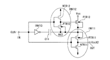
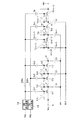
<昇圧回路(1)>
以下、本発明の第1の実施の形態における2倍昇圧回路について図1を参照しつつ説明する。図1は本実施の形態における2倍昇圧回路の構成を示す回路図である。なお、使用するクロック信号CLKの波高値(振幅)をVccとし、この反転信号CLKrが入力端INに入力される。
ソースに電源電圧Vccが入力される、充電用のP型電界効果トランジスタ(以下、Pchトランジスタという。)PTR13がある。PchトランジスタPTR13の基盤(N−Well)はPchトランジスタPTR13のドレインに接続される。一端がPchトランジスタPTR13のドレインに接続され、他端がインバータ回路INV13の出力端に接続されたキャパシタC11がある。このキャパシタC11の他端にはクロック信号CLK(クロック信号CLKの反転信号CLKrがインバータ回路INV13で反転されて得られるクロック信号CLK)が供給される。
<Boost circuit (1)>
The double booster circuit according to the first embodiment of the present invention will be described below with reference to FIG. FIG. 1 is a circuit diagram showing a configuration of a double booster circuit according to the present embodiment. The peak value (amplitude) of the clock signal CLK to be used is Vcc, and this inverted signal CLKr is input to the input terminal IN.
There is a P-type field effect transistor (hereinafter referred to as a Pch transistor)
インバータ回路INV11があり、インバータ回路INV11には、PchトランジスタPTR11とNchトランジスタNTR11とが含まれている。
PchトランジスタPTR11の基盤(N−Well)はPchトランジスタPTR11のソースに接続される。
PchトランジスタPTR11のゲートとNchトランジスタNTR11のゲートとが接続されており、その接続点(インバータ回路INV11の入力部)にクロック信号CLKの反転信号CLKrが入力される。
PchトランジスタPTR11のドレインとNchトランジスタNTR11のドレインとが接続されており、その接続点(インバータ回路INV11の出力部)が2倍昇圧回路の出力端OUTに接続されている。
PchトランジスタPTR11のソース、つまり、インバータ回路INV11の電源端子はキャパシタC11の一端に接続されている。
NchトランジスタNTR11のソースは接地されている。
There is an inverter circuit INV11, and the inverter circuit INV11 includes a Pch transistor PTR11 and an Nch transistor NTR11.
The base (N-Well) of the Pch transistor PTR11 is connected to the source of the Pch transistor PTR11.
The gate of the Pch transistor PTR11 and the gate of the Nch transistor NTR11 are connected, and an inverted signal CLKr of the clock signal CLK is input to the connection point (input portion of the inverter circuit INV11).
The drain of the Pch transistor PTR11 and the drain of the Nch transistor NTR11 are connected, and the connection point (the output part of the inverter circuit INV11) is connected to the output terminal OUT of the double booster circuit.
The source of the Pch transistor PTR11, that is, the power supply terminal of the inverter circuit INV11 is connected to one end of the capacitor C11.
The source of the Nch transistor NTR11 is grounded.
インバータ回路INV12があり、インバータ回路INV12には、PchトランジスタPTR12とNchトランジスタNTR12とが含まれている。
PchトランジスタPTR12の基盤(N−Well)はPchトランジスタPTR12のソースに接続される。
PchトランジスタPTR12のゲートとNchトランジスタNTR12のゲートとが接続されており、その接続点(インバータ回路INV12の入力部)にクロック信号CLKの反転信号CLKrが入力される。
PchトランジスタPTR12のドレインとNchトランジスタNTR12のドレインとが接続されており、その接続点(インバータ回路INV12の出力部)はPchトランジスタPTR13のゲートに接続されている。
PchトランジスタPTR12のソース、つまり、インバータ回路INV12の電源端子はキャパシタC11の一端に接続されている。
NchトランジスタNTR12のソースは接地されている。
There is an inverter circuit INV12, and the inverter circuit INV12 includes a Pch transistor PTR12 and an Nch transistor NTR12.
The base (N-Well) of the Pch transistor PTR12 is connected to the source of the Pch transistor PTR12.
The gate of the Pch transistor PTR12 and the gate of the Nch transistor NTR12 are connected, and an inverted signal CLKr of the clock signal CLK is input to the connection point (input portion of the inverter circuit INV12).
The drain of the Pch transistor PTR12 and the drain of the Nch transistor NTR12 are connected, and the connection point (the output part of the inverter circuit INV12) is connected to the gate of the Pch transistor PTR13.
The source of the Pch transistor PTR12, that is, the power supply terminal of the inverter circuit INV12 is connected to one end of the capacitor C11.
The source of the Nch transistor NTR12 is grounded.
次に、図1を参照しつつ回路構成を説明した本実施の形態における2倍昇圧回路の動作について図2を参照しつつ説明する。図2は図1の昇圧回路の動作を説明するための波形図である。
クロック信号CLKがLレベルのとき、つまりその反転信号CLKrがHレベルのとき、NchトランジスタNTR11のゲートおよびPchトランジスタPTR11のゲートにHレベルが入力されるので、NchトランジスタNTR11側がONし、出力端OUTへ接地レベル、つまりLレベルが出力される。
このとき、NchトランジスタNTR12のゲートおよびPchトランジスタPTR12のゲートにHレベルが入力されるので、NchトランジスタNTR12側がONし、PchトランジスタPTR13のゲートに接地レベル、つまりLレベルが入力され、PchトランジスタPTR11がONし、PchトランジスタPTR13を通して、電源電圧Vccでキャパシタ11が充電され、Vcc分の電荷量が蓄えられる(図2参照)。
Next, the operation of the double booster circuit in the present embodiment whose circuit configuration has been described with reference to FIG. 1 will be described with reference to FIG. FIG. 2 is a waveform diagram for explaining the operation of the booster circuit of FIG.
When the clock signal CLK is at the L level, that is, when the inverted signal CLKr is at the H level, the H level is input to the gate of the Nch transistor NTR11 and the gate of the Pch transistor PTR11, so the Nch transistor NTR11 side is turned on and the output terminal OUT The ground level, that is, the L level is output.
At this time, since the H level is input to the gate of the Nch transistor NTR12 and the gate of the Pch transistor PTR12, the Nch transistor NTR12 side is turned ON, the ground level, that is, the L level is input to the gate of the Pch transistor PTR13, and the Pch transistor PTR11 is The capacitor 11 is charged with the power supply voltage Vcc through the Pch transistor PTR13, and a charge amount corresponding to Vcc is stored (see FIG. 2).
その後、クロック信号CLKがHレベル、つまりその反転信号CLKrがLレベルとなると、NchトランジスタNTR12のゲートおよびPchトランジスタPTR12のゲートにLレベルが入力されるので、PchトランジスタPTR12側がONし、PchトランジスタPTR13のゲートにHレベルが入力され、PchトランジスタPTR13がOFFする。
また、反転信号CLKrがLレベルのとき、NchトランジスタNTR11のゲートおよびPchトランジスタPTR11のゲートにLレベルが入力されるので、NchトランジスタNTR11がOFFし、PchトランジスタPTR11がONする。
このとき、インバータ回路INV13の出力がLレベルからHレベルになっているので、キャパシタC11にVccレベルの電圧が供給されて、ノードNV2の電位はほぼ2×Vccとなっており、このほぼ2×Vccレベルの信号がPchトランジスタPTR11を通って出力端OUTへ出力される(図2参照)。
After that, when the clock signal CLK becomes H level, that is, the inverted signal CLKr becomes L level, L level is input to the gate of the Nch transistor NTR12 and the gate of the Pch transistor PTR12, so that the Pch transistor PTR12 side is turned on and the Pch transistor PTR13 H level is input to the gate of Pch, and the Pch transistor PTR13 is turned OFF.
When inverted signal CLKr is at L level, L level is input to the gate of Nch transistor NTR11 and the gate of Pch transistor PTR11, so that Nch transistor NTR11 is turned off and Pch transistor PTR11 is turned on.
At this time, since the output of the inverter circuit INV13 is changed from the L level to the H level, the voltage of the Vcc level is supplied to the capacitor C11, and the potential of the node NV2 is approximately 2 × Vcc, and this approximately 2 × A signal at the Vcc level is output to the output terminal OUT through the Pch transistor PTR11 (see FIG. 2).
以上のように、本実施の形態によれば、素子数の少ない簡単な構成で、クロック信号CLKの波高値(振幅)を2倍に昇圧し、波高値(振幅)が2×Vccのクロック信号を出力する2倍昇圧回路を実現することができる。そして、2倍昇圧回路の素子数が少ないため2倍昇圧回路に必要な面積が小さいという利点がある。 As described above, according to the present embodiment, the peak value (amplitude) of the clock signal CLK is boosted twice by a simple configuration with a small number of elements, and the clock signal having a peak value (amplitude) of 2 × Vcc. Can be realized. Since the number of elements of the double booster circuit is small, there is an advantage that the area required for the double booster circuit is small.
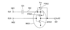
<昇圧回路(2)>
以下、本発明の第2の実施の形態における2倍昇圧回路について図3を参照しつつ説明する。図3は本実施の形態における2倍昇圧回路の構成を示す回路図である。なお、使用するクロック信号CLKの波高値(振幅)をVccとし、クロック信号CLKが入力端IN21に、クロック信号CLKの反転信号CLKrが入力端IN22に入力される。
ソースに電源電圧Vccが入力される、充電用のPchトランジスタPTR22がある。PchトランジスタPTR22の基盤(N−Well)はPchトランジスタPTR22のドレインに接続される。一端がPchトランジスタPTR22のドレインに接続され、他端が入力端IN21に接続されたキャパシタC21がある。
<Boost circuit (2)>
The double booster circuit according to the second embodiment of the present invention will be described below with reference to FIG. FIG. 3 is a circuit diagram showing the configuration of the double booster circuit in the present embodiment. The peak value (amplitude) of the clock signal CLK to be used is Vcc, the clock signal CLK is input to the input terminal IN21, and the inverted signal CLKr of the clock signal CLK is input to the input terminal IN22.
There is a Pch transistor PTR22 for charging in which a power supply voltage Vcc is input to the source. The base (N-Well) of the Pch transistor PTR22 is connected to the drain of the Pch transistor PTR22. There is a capacitor C21 having one end connected to the drain of the Pch transistor PTR22 and the other end connected to the input terminal IN21.
インバータ回路INV21があり、インバータ回路INV21には、PchトランジスタPTR21とNchトランジスタNTR21とが含まれている。
PchトランジスタPTR21の基盤(N−Well)はPchトランジスタPTR21のソースに接続される。
PchトランジスタPTR21のゲートとNchトランジスタNTR21のゲートとが接続されており、その接続点(インバータ回路INV21の入力部)に入力端IN22が接続される。
PchトランジスタPTR21のドレインとNchトランジスタNTR21のドレインとが接続されており、その接続点(インバータ回路INV21の出力部)に2倍昇圧回路の出力端OUTが接続されているとともに、接続点はPchトランジスタPTR22のゲートにも接続されている。
PchトランジスタPTR21のソース、つまり、インバータ回路INV21の電源端子はキャパシタC21の一端に接続されている。
NchトランジスタNTR21のソースは接地されている。
There is an inverter circuit INV21, and the inverter circuit INV21 includes a Pch transistor PTR21 and an Nch transistor NTR21.
The base (N-Well) of the Pch transistor PTR21 is connected to the source of the Pch transistor PTR21.
The gate of the Pch transistor PTR21 and the gate of the Nch transistor NTR21 are connected, and the input terminal IN22 is connected to the connection point (the input part of the inverter circuit INV21).
The drain of the Pch transistor PTR21 and the drain of the Nch transistor NTR21 are connected, the output terminal OUT of the double booster circuit is connected to the connection point (the output part of the inverter circuit INV21), and the connection point is the Pch transistor. It is also connected to the gate of the PTR 22.
The source of the Pch transistor PTR21, that is, the power supply terminal of the inverter circuit INV21 is connected to one end of the capacitor C21.
The source of the Nch transistor NTR21 is grounded.
ここで、図3を参照しつつ回路構成を説明した本実施の形態における2倍昇圧回路の動作について説明する。
クロック信号CLKがLレベルのとき、つまりその反転信号CLKrはHレベルのとき、NchトランジスタNTR21のゲートおよびPchトランジスタPTR21のゲートにHレベルが入力されるので、NchトランジスタNTR21側がONし、出力端OUTへ接地レベル、つまりLレベルが出力される。このとき、Pchトランジスタ22のゲートに接地レベル、つまりLレベルが入力され、PchトランジスタPTR22がONし、PchトランジスタPTR22を通して、電源電圧VccでキャパシタC21が充電され、Vcc分の電荷量が蓄えられる。
Here, the operation of the double booster circuit in the present embodiment whose circuit configuration has been described with reference to FIG. 3 will be described.
When the clock signal CLK is at the L level, that is, when the inverted signal CLKr is at the H level, the H level is input to the gate of the Nch transistor NTR21 and the gate of the Pch transistor PTR21, so the Nch transistor NTR21 side is turned on and the output terminal OUT The ground level, that is, the L level is output. At this time, the ground level, that is, the L level is input to the gate of the Pch transistor 22, the Pch transistor PTR 22 is turned on, the
その後、クロック信号CLKがHレベル、つまりその反転信号CLKrがLレベルとなると、NchトランジスタNTR21のゲートおよびPchトランジスタPTR21のゲートにLレベルが入力されるので、NchトランジスタNTR21がOFFし、PchトランジスタPTR21がONし、出力VoutがほぼVccレベルに充電されるため、PchトランジスタPTR22のゲートにHレベルが入力され、PchトランジスタPTR22がOFFする。
このとき、キャパシタC21にVccレベルの電圧が供給されているため、ノードNV2の電位はほぼ2×Vccとなっており、このほぼ2×Vccレベルの信号がPchトランジスタPTR21を通って出力端OUTへ出力される。
After that, when the clock signal CLK becomes H level, that is, the inverted signal CLKr becomes L level, L level is input to the gate of the Nch transistor NTR21 and the gate of the Pch transistor PTR21, so that the Nch transistor NTR21 is turned OFF and the Pch transistor PTR21. Is turned on, and the output Vout is charged to approximately the Vcc level, so that the H level is input to the gate of the Pch transistor PTR22 and the Pch transistor PTR22 is turned off.
At this time, since the Vcc level voltage is supplied to the capacitor C21, the potential of the node NV2 is approximately 2 × Vcc, and the approximately 2 × Vcc level signal passes through the Pch transistor PTR21 to the output terminal OUT. Is output.
以上のように、本実施の形態によれば、素子数の少ない簡単な構成で、クロック信号CLKの波高値(振幅)を2倍に昇圧し、波高値(振幅)が2倍になったクロック信号を出力する2倍昇圧回路を実現することができる。そして、第2の実施の形態の2倍昇圧回路は第1の実施の形態の2倍昇圧回路より素子数がさらに少なくなっているため2倍昇圧回路に必要な面積がより小さくなるという利点がある。 As described above, according to the present embodiment, with a simple configuration having a small number of elements, the crest value (amplitude) of the clock signal CLK is doubled and the crest value (amplitude) is doubled. A double boosting circuit that outputs a signal can be realized. The double booster circuit according to the second embodiment has an advantage that the area required for the double booster circuit is smaller because the number of elements is further reduced as compared with the double booster circuit according to the first embodiment. is there.
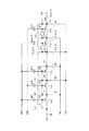
<昇圧回路(3)>
以下、本発明の第3の実施の形態における3倍昇圧回路について図4を参照しつつ説明する。図4は本実施の形態における3倍昇圧回路の構成を示す回路図である。なお、使用するクロック信号CLKの波高値(振幅)をVccとし、クロック信号CLKが入力端IN31に、クロック信号CLKの反転信号CLKrが入力端IN32,33に入力される。
ソースに電源電圧Vccが入力される、充電用のPchトランジスタPTR32がある。PchトランジスタPTR32の基盤(N−Well)はPchトランジスタPTR32のドレインに接続される。一端がPchトランジスタPTR32のドレインに接続され、他端が入力端IN31に接続されたキャパシタC31がある。
<Boost circuit (3)>
Hereinafter, a triple booster circuit according to a third embodiment of the present invention will be described with reference to FIG. FIG. 4 is a circuit diagram showing a configuration of the triple booster circuit according to the present embodiment. The peak value (amplitude) of the clock signal CLK to be used is Vcc, the clock signal CLK is input to the input terminal IN31, and the inverted signal CLKr of the clock signal CLK is input to the input terminals IN32 and 33.
There is a charging Pch transistor PTR32 to which a power supply voltage Vcc is input. The base (N-Well) of the Pch transistor PTR32 is connected to the drain of the Pch transistor PTR32. There is a capacitor C31 having one end connected to the drain of the Pch transistor PTR32 and the other end connected to the input terminal IN31.
インバータ回路INV31があり、インバータ回路INV31には、PchトランジスタPTR31とNchトランジスタNTR31とが含まれている。
PchトランジスタPTR31の基盤(N−Well)はPchトランジスタPTR31のソースに接続される。
PchトランジスタPTR31のゲートとNchトランジスタNTR31のゲートとが接続されており、その接続点(インバータ回路INV31の入力部)に入力端IN32が接続される。
PchトランジスタPTR31のドレインとNchトランジスタNTR31のドレインとが接続されており、その接続点(インバータ回路INV31の出力部)にPchトランジスタPTR34のソースが接続されているとともに、接続点はPchトランジスタPTR32のゲートにも接続されている。
PchトランジスタPTR31のソース、つまり、インバータ回路INV31の電源端子はキャパシタC31の一端に接続されている。
NchトランジスタNTR31のソースは接地されている。
PchトランジスタPTR32、キャパシタC31、インバータ回路INV31で、入力されるクロック信号CLKを2×Vccの波高値(振幅)のクロック信号に昇圧する昇圧回路が構成されており、1段目の昇圧回路部と呼ぶ。
There is an inverter circuit INV31, and the inverter circuit INV31 includes a Pch transistor PTR31 and an Nch transistor NTR31.
The base (N-Well) of the Pch transistor PTR31 is connected to the source of the Pch transistor PTR31.
The gate of the Pch transistor PTR31 and the gate of the Nch transistor NTR31 are connected, and the input terminal IN32 is connected to the connection point (the input part of the inverter circuit INV31).
The drain of the Pch transistor PTR31 and the drain of the Nch transistor NTR31 are connected, the source of the Pch transistor PTR34 is connected to the connection point (the output part of the inverter circuit INV31), and the connection point is the gate of the Pch transistor PTR32. Also connected to.
The source of the Pch transistor PTR31, that is, the power supply terminal of the inverter circuit INV31 is connected to one end of the capacitor C31.
The source of the Nch transistor NTR31 is grounded.
The Pch transistor PTR32, the capacitor C31, and the inverter circuit INV31 constitute a booster circuit that boosts the input clock signal CLK to a clock signal having a peak value (amplitude) of 2 × Vcc. Call.
ソースが1段目の昇圧回路部のインバータ回路INV31の出力部に接続された、充電用のPchトランジスタPTR34がある。PchトランジスタPTR34の基盤(N−Well)はPchトランジスタPTR34のソースに接続される。一端がPchトランジスタPTR34のドレインに接続され、他端が入力端IN33に接続されたキャパシタC32がある。 There is a charging Pch transistor PTR34 whose source is connected to the output part of the inverter circuit INV31 of the first booster circuit part. The base (N-Well) of the Pch transistor PTR34 is connected to the source of the Pch transistor PTR34. There is a capacitor C32 having one end connected to the drain of the Pch transistor PTR34 and the other end connected to the input end IN33.
インバータ回路INV33があり、インバータ回路INV33には、PchトランジスタPTR33とNchトランジスタNTR33とが含まれている。
PchトランジスタPTR33の基盤(N−Well)はPchトランジスタPTR33のソースに接続される。
PchトランジスタPTR33のゲートとNchトランジスタNTR33のゲートとが接続されており、その接続点(インバータ回路INV33の入力部)に1段目の昇圧回路部のインバータ回路INV31の出力部が接続される。
PchトランジスタPTR33のドレインとNchトランジスタNTR33のドレインとが接続されており、その接続点(インバータ回路INV33の出力部)に3倍昇圧回路の出力端OUTが接続されているとともに、接続点はPchトランジスタPTR34のゲートにも接続されている。
PchトランジスタPTR33のソース、つまり、インバータ回路INV33の電源端子はキャパシタC32の一端に接続されている。
NchトランジスタNTR33のソースは接地されている。
PchトランジスタPTR34、キャパシタC32、インバータ回路INV33で、1段目の昇圧回路部で得られる波高値(振幅)が2×Vccのクロック信号を3×Vccの波高値(振幅)のクロック信号に昇圧する昇圧回路部が構成されており、2段目の昇圧回路部と呼ぶ。
There is an inverter circuit INV33, and the inverter circuit INV33 includes a Pch transistor PTR33 and an Nch transistor NTR33.
The base (N-Well) of the Pch transistor PTR33 is connected to the source of the Pch transistor PTR33.
The gate of the Pch transistor PTR33 and the gate of the Nch transistor NTR33 are connected, and the output part of the inverter circuit INV31 of the first-stage booster circuit part is connected to the connection point (input part of the inverter circuit INV33).
The drain of the Pch transistor PTR33 and the drain of the Nch transistor NTR33 are connected, and the output terminal OUT of the triple booster circuit is connected to the connection point (the output part of the inverter circuit INV33). It is also connected to the gate of the
The source of the Pch transistor PTR33, that is, the power supply terminal of the inverter circuit INV33 is connected to one end of the capacitor C32.
The source of the Nch transistor NTR33 is grounded.
The Pch transistor PTR34, the capacitor C32, and the inverter circuit INV33 boost the clock signal having a peak value (amplitude) of 2 × Vcc obtained by the first-stage booster circuit unit to a clock signal having a peak value (amplitude) of 3 × Vcc. A booster circuit unit is configured and is referred to as a second-stage booster circuit unit.
次に、図4を参照しつつ回路構成を説明した本実施の形態における3倍昇圧回路の動作について図5を参照しつつ説明する。図5は図4の昇圧回路の動作を説明するための波形図である。
クロック信号CLKがLレベルのとき、つまりその反転信号CLKrがHレベルのとき、NchトランジスタNTR31のゲートおよびPchトランジスタPTR31のゲートにHレベルが入力されるので、NchトランジスタNTR31側がONして、インバータ回路INV31の出力は接地レベル、つまりLレベルとなり、接地レベルの信号がPchトランジスタPTR34のソースおよびインバータ回路INV33の入力部へ出力される。このとき、PchトランジスタPTR32のゲートに接地レベル、つまりLレベルが入力されるので、PchトランジスタPTR32がONして、PchトランジスタPTR32を通して、電源電圧VccでキャパシタC31が充電され、Vcc分の電荷量が蓄えられる(図5参照)。
Next, the operation of the triple booster circuit in the present embodiment whose circuit configuration has been described with reference to FIG. 4 will be described with reference to FIG. FIG. 5 is a waveform diagram for explaining the operation of the booster circuit of FIG.
When the clock signal CLK is at the L level, that is, when the inverted signal CLKr is at the H level, the H level is input to the gate of the Nch transistor NTR31 and the gate of the Pch transistor PTR31. The output of INV31 becomes the ground level, that is, the L level, and a signal of the ground level is output to the source of the Pch transistor PTR34 and the input part of the inverter circuit INV33. At this time, since the ground level, that is, the L level is input to the gate of the Pch transistor PTR32, the Pch transistor PTR32 is turned on, and the capacitor C31 is charged with the power supply voltage Vcc through the Pch transistor PTR32. Stored (see FIG. 5).
その後、クロック信号CLKがHレベル、つまりその反転信号CLKrがLレベルとなると、NchトランジスタNTR31のゲートおよびPchトランジスタPTR31のゲートにLレベルが入力されるので、PchトランジスタPTR31側がONして、PchトランジスタPTR32のゲートにHレベルが入力され、PchトランジスタPTR32がOFFする。
このとき、キャパシタC31にVccレベルの電圧が供給されているため、ノードNV2の電位はほぼ2×Vccとなっており、このほぼ2×Vccレベルの信号がPchトランジスタPTR31を通って次段の昇圧回路部(2段目の昇圧回路部)のPchトランジスタPTR34のソースおよびインバータ回路INV33の入力部へ出力される(図5参照)。
After that, when the clock signal CLK becomes H level, that is, the inverted signal CLKr becomes L level, L level is inputted to the gate of the Nch transistor NTR31 and the gate of the Pch transistor PTR31, so that the Pch transistor PTR31 side is turned on and the Pch transistor The H level is input to the gate of the
At this time, since the Vcc level voltage is supplied to the capacitor C31, the potential of the node NV2 is approximately 2 × Vcc, and the approximately 2 × Vcc level signal passes through the Pch transistor PTR31 and is boosted in the next stage. The signal is output to the source of the Pch transistor PTR34 in the circuit section (second booster circuit section) and the input section of the inverter circuit INV33 (see FIG. 5).
つまり、1段目の昇圧回路部は、2段目の昇圧回路部のNchトランジスタPTR34のソースへ、クロック信号CLKがLレベルのときに接地レベルの信号を出力し、クロック信号CLKがHレベルのときに2×Vccレベルの信号を出力する。 That is, the first stage booster circuit unit outputs a ground level signal to the source of the Nch transistor PTR34 of the second stage booster circuit unit when the clock signal CLK is at L level, and the clock signal CLK is at H level. Sometimes a signal of 2 × Vcc level is output.
クロック信号CLKがHレベルのとき、即ちインバータ回路INV31の出力部がHレベルのとき、NchトランジスタNTR33のゲートおよびPchトランジスタPTR33のゲートにHレベルが入力されるので、NchトランジスタNTR33側がONして、接地レベル、つまりLレベルが3倍昇圧回路の出力端OUTへ出力される。このとき、PchトランジスタPTR34のゲートに接地レベル、つまりLレベルが入力されるので、PchトランジスタPTR34がONして、PchトランジスタPTR34を通して、1段目の昇圧回路部から入力されている2×Vccでキャパシタ32が充電され、2×Vcc分の電荷量が蓄えられる(図5参照)。
When the clock signal CLK is at the H level, that is, when the output part of the inverter circuit INV31 is at the H level, the H level is input to the gate of the Nch transistor NTR33 and the gate of the Pch transistor PTR33, so that the Nch transistor NTR33 side is turned on. The ground level, that is, the L level is output to the output terminal OUT of the triple booster circuit. At this time, since the ground level, that is, the L level is input to the gate of the Pch transistor PTR34, the Pch transistor PTR34 is turned ON, and 2 × Vcc inputted from the first-stage booster circuit section through the Pch transistor PTR34. The
その後、クロック信号CLKがLレベルとなると、インバータ回路INV31の出力がLレベルになり、NchトランジスタNTR33のゲートおよびPchトランジスタPTR33のゲートにLレベルが入力されるので、PchトランジスタPTR33側がONして、PchトランジスタPTR34のゲートにHレベルが入力され、PchトランジスタPTR34がOFFする。
このとき、キャパシタC32にVccレベルの電圧が供給されているため、ノードNV3の電位はほぼ3×Vccとなっており、このほぼ3×Vccレベルの信号がPchトランジスタPTR33を通って出力端OUTへ出力される(図5参照)。
After that, when the clock signal CLK becomes L level, the output of the inverter circuit INV31 becomes L level, and the L level is input to the gate of the Nch transistor NTR33 and the gate of the Pch transistor PTR33, so that the Pch transistor PTR33 side is turned ON, The H level is input to the gate of the Pch transistor PTR34, and the Pch transistor PTR34 is turned OFF.
At this time, since the Vcc level voltage is supplied to the capacitor C32, the potential of the node NV3 is approximately 3 × Vcc, and the approximately 3 × Vcc level signal passes through the Pch transistor PTR33 to the output terminal OUT. Is output (see FIG. 5).
以上のように、本実施の形態によれば、素子数の少ない簡単な構成で、クロック信号CLKの波高値(振幅)を3倍に昇圧し、波高値(振幅)が3倍になったクロック信号を出力する3倍昇圧回路を実現することができる。そして、3倍昇圧回路の素子数が少ないため3倍昇圧回路に必要な面積が小さいという利点がある。 As described above, according to the present embodiment, with a simple configuration having a small number of elements, the crest value (amplitude) of the clock signal CLK is boosted three times, and the crest value (amplitude) is tripled. A triple booster circuit that outputs a signal can be realized. Since the number of elements of the triple booster circuit is small, there is an advantage that the area required for the triple booster circuit is small.
<昇圧回路(4)>
以下、本発明の第4の実施の形態におけるn倍昇圧回路について図6を参照しつつ説明する。図6は本実施の形態におけるn倍昇圧回路の構成を示す回路図である。なお、使用されるクロック信号CLKの波高値(振幅)をVccとする。
図6のn倍昇圧回路は、図4の第3の実施の形態における3倍昇圧回路を応用したものであり、図4の1段目の昇圧回路部、2段目の昇圧回路部、1段目の昇圧回路部、・・・と接続することによって構成される。
<Boost circuit (4)>
The n-fold booster circuit according to the fourth embodiment of the present invention will be described below with reference to FIG. FIG. 6 is a circuit diagram showing a configuration of the n-fold booster circuit according to the present embodiment. The peak value (amplitude) of the clock signal CLK used is Vcc.
The n-fold booster circuit in FIG. 6 is an application of the triple booster circuit in the third embodiment of FIG. 4. The first-stage booster circuit unit, the second-stage booster circuit unit in FIG. It is configured by connecting to the booster circuit unit at the stage.
図中の昇圧回路A1,A3,・・・,A(n−2)は図4の1段目の昇圧回路部(PchトランジスタPTR32,キャパシタC31,インバータ回路INV31よりなる回路部)により構成されている。ただし、昇圧回路A1のPchトランジスタPTR32のソースには電源電圧Vccが接続され、他の昇圧回路A3,・・・,A(n−2)のPchトランジスタPTR32のソースには1段前の昇圧回路A2,・・・,A(n−3)のインバータ回路INV33の出力部(PchトランジスタPTR33のドレインとNchトランジスタNTR33のドレインとの接続点)が接続されている。また、昇圧回路A1のインバータ回路INV31の入力部にはクロック信号CLKの反転信号CLKrが入力され、他の昇圧回路A3,・・・A(n−2)のインバータ回路INV31の入力部には1段前の昇圧回路A2,・・・A(n−3)のインバータ回路INV33の出力部が接続されている。なお、図4の場合と同様、キャパシタC31側にクロック信号CLKが入力される。 The booster circuits A1, A3,..., A (n-2) in the figure are configured by the first-stage booster circuit part (a circuit part comprising a Pch transistor PTR32, a capacitor C31, and an inverter circuit INV31) in FIG. Yes. However, the power supply voltage Vcc is connected to the source of the Pch transistor PTR32 of the booster circuit A1, and the source of the Pch transistor PTR32 of the other booster circuits A3,... The output part of the inverter circuit INV33 of A2,..., A (n-3) (the connection point between the drain of the Pch transistor PTR33 and the drain of the Nch transistor NTR33) is connected. Further, an inverted signal CLKr of the clock signal CLK is input to the input part of the inverter circuit INV31 of the booster circuit A1, and 1 is input to the input part of the inverter circuit INV31 of the other booster circuits A3,... A (n-2). The output part of the inverter circuit INV33 of the booster circuits A2,... A (n-3) before the stage is connected. As in the case of FIG. 4, the clock signal CLK is input to the capacitor C31 side.
図中の昇圧回路A2,A4,・・・,A(n−1)は図4の2段目の昇圧回路部(PchトランジスタPTR34,キャパシタC32,インバータ回路INV33よりなる回路部)により構成されている。ただし、昇圧回路A2,A4,・・・,A(n−1)のPchトランジスタPTR34のソースおよびインバータ回路INV33の入力部には1段前の昇圧回路A1,A3,・・・,A(n−3)のインバータ回路INV31の出力部(PchトランジスタPTR31のドレインとNchトランジスタNTR31のドレインとの接続点)が接続されている。昇圧回路A(n−1)のインバータ回路INV33の出力部から出力されるクロック信号がn倍昇圧回路の出力となる。なお、図4の場合と同様、キャパシタC32側にクロック信号CLKの反転信号CLKrが入力される。 The booster circuits A2, A4,..., A (n−1) in the figure are configured by the second-stage booster circuit part (a circuit part comprising a Pch transistor PTR34, a capacitor C32, and an inverter circuit INV33) in FIG. Yes. However, the source of the Pch transistor PTR34 of the booster circuits A2, A4,..., A (n−1) and the input part of the inverter circuit INV33 are the booster circuits A1, A3,. -3) is connected to the output part of the inverter circuit INV31 (the connection point between the drain of the Pch transistor PTR31 and the drain of the Nch transistor NTR31). The clock signal output from the output part of the inverter circuit INV33 of the booster circuit A (n-1) is the output of the n-times booster circuit. As in the case of FIG. 4, an inverted signal CLKr of the clock signal CLK is input to the capacitor C32 side.
この構成では、昇圧回路A1から波高値(振幅)が2×Vccのクロック信号が昇圧回路A2のPchトランジスタPTR34へ出力され、昇圧回路A2から波高値(振幅)が3×Vccのクロック信号が昇圧回路A3のPchトランジスタPTR32へ出力される。昇圧回路A3から波高値(振幅)が4×Vccのクロック信号が昇圧回路A4のPchトランジスタPTR34へ出力される。順次行われることによって、昇圧回路A(n−1)から波高値(振幅)がn×Vccのクロック信号が出力され、n倍昇圧回路から波高値(振幅)がn×Vccのクロック信号が出力される。 In this configuration, a clock signal having a peak value (amplitude) of 2 × Vcc is output from the booster circuit A1 to the Pch transistor PTR34 of the booster circuit A2, and a clock signal having a peak value (amplitude) of 3 × Vcc is boosted from the booster circuit A2. It is output to the Pch transistor PTR32 of the circuit A3. A clock signal having a peak value (amplitude) of 4 × Vcc is output from the booster circuit A3 to the Pch transistor PTR34 of the booster circuit A4. By sequentially performing, a clock signal having a peak value (amplitude) of n × Vcc is output from the booster circuit A (n−1), and a clock signal having a peak value (amplitude) of n × Vcc is output from the n-fold booster circuit. Is done.
以上のように、本実施の形態によれば、素子数の少ない簡単な構成で、クロック信号CLKの波高値(振幅)をn倍に昇圧し、波高値(振幅)がn倍になったクロック信号を出力するn倍昇圧回路を実現することができる。そして、n昇圧回路の素子数が少ないためn倍昇圧回路に必要な面積が小さいという利点がある。 As described above, according to the present embodiment, with a simple configuration having a small number of elements, the crest value (amplitude) of the clock signal CLK is boosted n times, and the crest value (amplitude) is increased n times. An n-fold booster circuit that outputs a signal can be realized. Since the number of elements of the n booster circuit is small, there is an advantage that the area required for the n-fold booster circuit is small.
<昇圧回路(5)>
以下、本発明の第5の実施の形態における3倍昇圧回路について図7を参照しつつ説明する。図7は本実施の形態における3倍昇圧回路の構成を示す回路図である。なお、使用するクロック信号CLKの波高値(振幅)をVccとし、クロック信号CLKが入力端IN31aに、クロック信号CLKの反転信号CLKrが入力端IN32a,33aに入力される。
ソースに電源電圧Vccが入力される、充電用のPchトランジスタPTR32aがある。PchトランジスタPTR32aの基盤(N−Well)はPchトランジスタPTR32aのドレインに接続される。一端がPchトランジスタPTR32aのドレインに接続され、他端が入力端IN31aに接続されたキャパシタC31aがある。
<Boost circuit (5)>
The triple booster circuit according to the fifth embodiment of the present invention will be described below with reference to FIG. FIG. 7 is a circuit diagram showing the configuration of the triple booster circuit in the present embodiment. The peak value (amplitude) of the clock signal CLK to be used is Vcc, the clock signal CLK is input to the input terminal IN31a, and the inverted signal CLKr of the clock signal CLK is input to the input terminals IN32a and 33a.
There is a Pch transistor PTR 32a for charging in which a power supply voltage Vcc is input to the source. The base (N-Well) of the Pch transistor PTR32a is connected to the drain of the Pch transistor PTR32a. There is a capacitor C31a having one end connected to the drain of the Pch transistor PTR32a and the other end connected to the input end IN31a.
インバータ回路INV31aがあり、インバータ回路INV31aには、PchトランジスタPTR31aとNchトランジスタNTR31aとが含まれている。
PchトランジスタPTR31aの基盤(N−Well)はPchトランジスタPTR31aのソースに接続される。
PchトランジスタPTR31aのゲートとNchトランジスタNTR31aのゲートとが接続されており、その接続点(インバータ回路INV31aの入力部)に入力端IN32aが接続される。
PchトランジスタPTR31aのドレインとNchトランジスタNTR31aのドレインとが接続されており、その接続点(インバータ回路INV31aの出力部)はPchトランジスタPTR32aのゲートに接続されている。
PchトランジスタPTR31aのソース、つまり、インバータ回路INV31aの電源端子はキャパシタC31aの一端に接続されている。
NchトランジスタNTR31aのソースは接地されている。
PchトランジスタPTR32a、キャパシタC31a、インバータ回路INV31aで、入力されるクロック信号CLKを2×Vccの波高値(振幅)のクロック信号に昇圧する昇圧回路が構成されており、1段目の昇圧回路部と呼ぶ。
There is an inverter circuit INV31a, and the inverter circuit INV31a includes a Pch transistor PTR31a and an Nch transistor NTR31a.
The base (N-Well) of the Pch transistor PTR31a is connected to the source of the Pch transistor PTR31a.
The gate of the Pch transistor PTR31a and the gate of the Nch transistor NTR31a are connected, and the input terminal IN32a is connected to the connection point (the input part of the inverter circuit INV31a).
The drain of the Pch transistor PTR31a and the drain of the Nch transistor NTR31a are connected, and the connection point (the output part of the inverter circuit INV31a) is connected to the gate of the Pch transistor PTR32a.
The source of the Pch transistor PTR31a, that is, the power supply terminal of the inverter circuit INV31a is connected to one end of the capacitor C31a.
The source of the Nch transistor NTR31a is grounded.
The Pch transistor PTR32a, the capacitor C31a, and the inverter circuit INV31a constitute a booster circuit that boosts the input clock signal CLK to a clock signal having a peak value (amplitude) of 2 × Vcc. Call.
ソースが1段目の昇圧回路部の充電用のPchトランジスタPTR32aのドレイン(キャパシタC31aの一端)に接続された、充電用のPchトランジスタPTR34aがある。PchトランジスタPTR34aの基盤(N−Well)はPchトランジスタPTR34aのドレインに接続される。一端がPchトランジスタPTR34aのドレインに接続され、他端が入力端IN33aに接続されたキャパシタC32aがある。 There is a charging Pch transistor PTR 34a whose source is connected to the drain of the charging Pch transistor PTR 32a (one end of the capacitor C31a) of the first-stage booster circuit section. The base (N-Well) of the Pch transistor PTR 34a is connected to the drain of the Pch transistor PTR 34a. There is a capacitor C32a having one end connected to the drain of the Pch transistor PTR 34a and the other end connected to the input end IN33a.
インバータ回路INV33aがあり、インバータ回路INV33aには、PchトランジスタPTR33aとNchトランジスタNTR33aとが含まれている。
PchトランジスタPTR33aの基盤(N−Well)はPchトランジスタPTR33aのソースに接続される。
PchトランジスタPTR33aのゲートとNchトランジスタNTR33aのゲートとが接続されており、その接続点(インバータ回路INV33aの入力部)には1段目の昇圧回路部のインバータ回路INV31aの出力部が接続される。
PchトランジスタPTR33aのドレインとNchトランジスタNTR33aのドレインとが接続されており、その接続点(インバータ回路INV33aの出力部)に3倍昇圧回路の出力端OUTが接続されているとともに、接続点はPchトランジスタPTR34aのゲートにも接続されている。
PchトランジスタPTR33aのソース、つまり、インバータ回路INV33aの電源端子はキャパシタC32aの一端に接続されている。
NchトランジスタNTR33aのソースは接地されている。
PchトランジスタPTR34a、キャパシタC32a、インバータ回路INV33aで、1段目の昇圧回路部で得られる波高値(振幅)が2×Vccのクロック信号を3×Vccの波高値(振幅)のクロック信号に昇圧する昇圧回路部が構成されており、2段目の昇圧回路部と呼ぶ。
There is an inverter circuit INV33a, and the inverter circuit INV33a includes a Pch transistor PTR33a and an Nch transistor NTR33a.
The base (N-Well) of the Pch transistor PTR33a is connected to the source of the Pch transistor PTR33a.
The gate of the Pch transistor PTR33a and the gate of the Nch transistor NTR33a are connected, and the output point of the inverter circuit INV31a of the first-stage booster circuit portion is connected to the connection point (input portion of the inverter circuit INV33a).
The drain of the Pch transistor PTR33a and the drain of the Nch transistor NTR33a are connected, and the output terminal OUT of the triple booster circuit is connected to the connection point (the output part of the inverter circuit INV33a). It is also connected to the gate of the PTR 34a.
The source of the Pch transistor PTR33a, that is, the power supply terminal of the inverter circuit INV33a is connected to one end of the capacitor C32a.
The source of the Nch transistor NTR33a is grounded.
The Pch transistor PTR 34a, the capacitor C32a, and the inverter circuit INV33a boosts a clock signal having a peak value (amplitude) of 2 × Vcc obtained by the first-stage booster circuit unit to a clock signal having a peak value (amplitude) of 3 × Vcc. A booster circuit unit is configured and is referred to as a second-stage booster circuit unit.
ここで、図7を参照しつつ回路構成を説明した本実施の形態における3倍昇圧回路の動作について説明する。
クロック信号CLKがLレベルのとき、つまりその反転信号CLKrがHレベルのとき、NchトランジスタNTR31aのゲートおよびPchトランジスタPTR31aのゲートにHレベルが入力されるので、NchトランジスタNTR31a側がONして、インバータ回路INV31aの出力は接地レベル、つまりLレベルとなり、接地レベルの信号がインバータ回路INV33aの入力部へ出力される。このとき、Pchトランジスタ32aのゲートに接地レベル、つまりLレベルが入力されるので、PchトランジスタPTR32aがONし、PchトランジスタPTR32aを通して、電源電圧Vccでキャパシタ31aが充電され、Vcc分の電荷量が蓄えられる。
Here, the operation of the triple booster circuit in the present embodiment whose circuit configuration has been described with reference to FIG. 7 will be described.
When the clock signal CLK is at the L level, that is, when the inverted signal CLKr is at the H level, the H level is input to the gate of the Nch transistor NTR31a and the gate of the Pch transistor PTR31a. The output of the INV 31a becomes the ground level, that is, the L level, and the ground level signal is output to the input part of the inverter circuit INV33a. At this time, since the ground level, that is, the L level is input to the gate of the Pch transistor 32a, the Pch transistor PTR32a is turned on, and the capacitor 31a is charged with the power supply voltage Vcc through the Pch transistor PTR32a. It is done.
その後、クロック信号CLKがHレベル、つまりその反転信号CLKrがLレベルとなると、NchトランジスタNTR31aのゲートおよびPchトランジスタPTR31aのゲートにLレベルが入力されるので、PchトランジスタPTR31a側がONし、PchトランジスタPTR32aのゲートにHレベルが入力され、PchトランジスタPTR32aがOFFする。
このとき、キャパシタC31aにVccレベルの電圧が供給されているため、ノードNV2の電位はほぼ2×Vccとなっており、このほぼ2×Vccレベルの信号が次段の昇圧回路部(2段目の昇圧回路部)のPchトランジスタPTR34aのソースへ出力される。
After that, when the clock signal CLK becomes H level, that is, the inverted signal CLKr becomes L level, L level is input to the gate of the Nch transistor NTR31a and the gate of the Pch transistor PTR31a, so that the Pch transistor PTR31a side is turned on and the Pch transistor PTR32a The H level is input to the gate of Pch, and the Pch transistor PTR 32a is turned off.
At this time, since the voltage of the Vcc level is supplied to the capacitor C31a, the potential of the node NV2 is approximately 2 × Vcc, and the approximately 2 × Vcc level signal is applied to the next boost circuit section (second stage). Output to the source of the Pch transistor PTR 34a of the step-up circuit section).
つまり、1段目の昇圧回路部は、2段目の昇圧回路部のPchトランジスタPTR34aのソースへ、クロック信号CLKがLレベルのときにVccレベルの信号を出力し、クロック信号CLKがHレベルのときに2×Vccレベルの信号を出力する。また、インバータ回路INV33aへ、クロック信号CLKがLレベルのときLレベルの信号を出力し、クロック信号CLKがHレベルのとき、2×Vccレベルの信号を出力する。 That is, the first-stage booster circuit unit outputs a Vcc level signal to the source of the Pch transistor PTR 34a of the second-stage booster circuit unit when the clock signal CLK is at L level, and the clock signal CLK is at H level. Sometimes a signal of 2 × Vcc level is output. Further, when the clock signal CLK is at the L level, an L level signal is output to the inverter circuit INV33a, and when the clock signal CLK is at the H level, a 2 × Vcc level signal is output.
クロック信号CLKがHレベルのとき、NchトランジスタNTR33aのゲートおよびPchトランジスタPTR33aのゲートには1段目の昇圧回路部のインバータ回路INV31aの出力である2×Vccレベルが入力されるので、NchトランジスタNTR33a側がONし、且つPchトランジスタPTR33aは完全にOFFするため、接地レベル、つまりLレベルが3倍昇圧回路の出力端OUTへ出力される。このとき、Pchトランジスタ34aのゲートに接地レベル、つまりLレベルが入力されるので、PchトランジスタPTR34aがオンして、PchトランジスタPTR34aを通して、1段目の昇圧回路部から入力されている2×Vccでキャパシタ32aが充電され、2×Vcc分の電荷量が蓄えられる。 When the clock signal CLK is at the H level, the 2 × Vcc level that is the output of the inverter circuit INV31a of the first-stage booster circuit section is input to the gate of the Nch transistor NTR33a and the gate of the Pch transistor PTR33a, and thus the Nch transistor NTR33a Since the Pch transistor PTR33a is completely turned off, the ground level, that is, the L level is output to the output terminal OUT of the triple booster circuit. At this time, since the ground level, that is, the L level is inputted to the gate of the Pch transistor 34a, the Pch transistor PTR 34a is turned on, and 2 × Vcc inputted from the first-stage booster circuit section through the Pch transistor PTR 34a. The capacitor 32a is charged and a charge amount of 2 × Vcc is stored.
その後、クロック信号CLKがLレベルとなると、NchトランジスタNTR33aのゲートおよびPchトランジスタPTR33aのゲートにインバータ回路INV31aの出力であるLレベルが入力されるので、PchトランジスタPTR33a側がONして、PchトランジスタPTR34aのゲートに2×Vccレベルが入力され、PchトランジスタPTR34aがOFFする。
このとき、キャパシタC32aにVccレベルの電圧が供給されているため、ノードNV3の電位はほぼ3×Vccとなっており、このほぼ3×Vccレベルの信号がPchトランジスタPTR33aを通って出力端OUTへ出力される。
Thereafter, when the clock signal CLK becomes L level, the L level that is the output of the inverter circuit INV31a is input to the gate of the Nch transistor NTR33a and the gate of the Pch transistor PTR33a, so that the Pch transistor PTR33a side is turned on, and the Pch transistor PTR34a side The 2 × Vcc level is input to the gate, and the Pch transistor PTR 34a is turned OFF.
At this time, since the Vcc level voltage is supplied to the capacitor C32a, the potential of the node NV3 is approximately 3 × Vcc, and the approximately 3 × Vcc level signal passes through the Pch transistor PTR33a to the output terminal OUT. Is output.
以上のように、本実施の形態によれば、素子数の少ない簡単な構成で、クロック信号CLKの波高値(振幅)を3倍に昇圧し、波高値(振幅)が3倍になったクロック信号を出力する3倍昇圧回路を実現することができる。そして、3倍昇圧回路の素子数が少ないため3倍昇圧回路に必要な面積が小さいという利点がある。 As described above, according to the present embodiment, with a simple configuration having a small number of elements, the crest value (amplitude) of the clock signal CLK is boosted three times, and the crest value (amplitude) is tripled. A triple booster circuit that outputs a signal can be realized. Since the number of elements of the triple booster circuit is small, there is an advantage that the area required for the triple booster circuit is small.
<昇圧回路(6)>
以下、本発明の第6の実施の形態におけるn倍昇圧回路について図8を参照しつつ説明する。図8は本実施の形態におけるn倍昇圧回路の構成を示す回路図である。なお、使用されるクロック信号CLKの波高値(振幅)をVccとする。
図8のn倍昇圧回路は、図7の第5の実施の形態における3倍昇圧回路を応用したものであり、図7の1段目の昇圧回路部、2段目の昇圧回路部、1段目の昇圧回路部、・・・と接続することによって構成される。
<Boost circuit (6)>
The n-fold booster circuit according to the sixth embodiment of the present invention will be described below with reference to FIG. FIG. 8 is a circuit diagram showing a configuration of the n-fold booster circuit according to the present embodiment. The peak value (amplitude) of the clock signal CLK used is Vcc.
The n-fold booster circuit in FIG. 8 is an application of the triple booster circuit in the fifth embodiment in FIG. 7. The first-stage booster circuit unit, the second-stage booster circuit unit in FIG. It is configured by connecting to the booster circuit unit at the stage.
図中の昇圧回路A1a,A3a,・・・,A(n−2)aは図7の1段目の昇圧回路部(PchトランジスタPTR32a,キャパシタC31a,インバータ回路INV31aよりなる回路部)により構成されている。ただし、昇圧回路A1aのPchトランジスタPTR32aのソースには電源電圧Vccが接続され、他の昇圧回路A3a,・・・,A(n−2)aのPchトランジスタPTR32aのソースには1段前の昇圧回路A2a,・・・,A(n−3)aのPchトンランジスタPTR34aのドレイン(キャパシタC32aの一端)が接続され、且つ、インバータ回路INV31aの入力部には、同じく1段前の昇圧回路A2a,・・・A(n−3)aのインバータ回路INV33aの出力部(PchトランジスタPTR33aのドレインとNchトランジスタNTR33aのドレインとの接続点)が接続されている。なお、図7の場合と同様、キャパシタC31a側にクロック信号CLKが入力される。 In FIG. 7, booster circuits A1a, A3a,..., A (n-2) a are configured by the first-stage booster circuit unit (a circuit unit including a Pch transistor PTR32a, a capacitor C31a, and an inverter circuit INV31a) in FIG. ing. However, the power supply voltage Vcc is connected to the source of the Pch transistor PTR32a of the booster circuit A1a, and the source of the Pch transistor PTR32a of the other booster circuits A3a,... The drain of the Pch transistor PTR 34a (one end of the capacitor C32a) of the circuit A2a,..., A (n-3) a is connected, and the input circuit of the inverter circuit INV31a is similarly connected to the previous boost circuit A2a. ,... Are connected to the output part of the inverter circuit INV33a of A (n-3) a (the connection point between the drain of the Pch transistor PTR33a and the drain of the Nch transistor NTR33a). As in the case of FIG. 7, the clock signal CLK is input to the capacitor C31a side.
図中の昇圧回路A2a,A4a,・・・,A(n−1)aは図7の2段目の昇圧回路部(PchトランジスタPTR34a,キャパシタC32a,インバータ回路INV33aよりなる回路部)により構成されている。ただし、昇圧回路A2a,A4a,・・・,A(n−1)aのPchトランジスタPTR34aのソースには1段前の昇圧回路A1a,A3a,・・・,A(n−2)aのPchトランジスタPTR32aのドレイン(キャパシタC31aの一端)が接続され、且つ、インバータ回路INV33aの入力部には、同じく1段前の昇圧回路A2a,・・・A(n−2)aのインバータ回路INV31aの出力部(PchトランジスタPTR31aのドレインとNchトランジスタNTR31aのドレインとの接続点)が接続されている。昇圧回路A(n−1)aのインバータ回路INV33aの出力部から出力されるクロック信号がn倍昇圧回路の出力となる。なお、図7の場合と同様、キャパシタC32a側にクロック信号CLKの反転信号CLKrが入力される。 The booster circuits A2a, A4a,..., A (n-1) a in the figure are configured by the second-stage booster circuit unit (a circuit unit including a Pch transistor PTR34a, a capacitor C32a, and an inverter circuit INV33a) in FIG. ing. However, the source of the Pch transistor PTR34a of the booster circuits A2a, A4a,..., A (n−1) a is connected to the Pch of the booster circuits A1a, A3a,. The drain of the transistor PTR32a (one end of the capacitor C31a) is connected, and the output of the inverter circuit INV31a of the previous boost circuit A2a,... A (n-2) a is connected to the input of the inverter circuit INV33a. (The connection point between the drain of the Pch transistor PTR31a and the drain of the Nch transistor NTR31a) is connected. The clock signal output from the output part of the inverter circuit INV33a of the booster circuit A (n-1) a becomes the output of the n-fold booster circuit. As in the case of FIG. 7, the inverted signal CLKr of the clock signal CLK is input to the capacitor C32a side.
この構成では、昇圧回路A1aから波高値(振幅)が2×Vccのクロック信号が昇圧回路A2aのPchトランジスタPTR34aへ出力され、昇圧回路A2aから波高値(振幅)が3×Vccのクロック信号が昇圧回路A3aのPchトランジスタPTR32aへ出力される。昇圧回路A3から波高値(振幅)が4×Vccのクロック信号が昇圧回路A4aのPchトランジスタPTR34へ出力される。順次行われることによって、昇圧回路A(n−1)から波高値(振幅)がn×Vccのクロック信号が出力され、n倍昇圧回路から波高値(振幅)がn×Vccのクロック信号が出力される。 In this configuration, a clock signal having a peak value (amplitude) of 2 × Vcc is output from the booster circuit A1a to the Pch transistor PTR 34a of the booster circuit A2a, and a clock signal having a peak value (amplitude) of 3 × Vcc is boosted from the booster circuit A2a. The signal is output to the Pch transistor PTR 32a of the circuit A3a. A clock signal having a peak value (amplitude) of 4 × Vcc is output from the booster circuit A3 to the Pch transistor PTR34 of the booster circuit A4a. By sequentially performing, a clock signal having a peak value (amplitude) of n × Vcc is output from the booster circuit A (n−1), and a clock signal having a peak value (amplitude) of n × Vcc is output from the n-fold booster circuit. Is done.
以上のように、本実施の形態によれば、素子数の少ない簡単な構成で、クロック信号CLKの波高値(振幅)をn倍に昇圧し、波高値(振幅)がn倍になったクロック信号を出力するn倍昇圧回路を実現することができる。そして、n昇圧回路の素子数が少ないためn倍昇圧回路に必要な面積が小さいという利点がある。 As described above, according to the present embodiment, with a simple configuration having a small number of elements, the crest value (amplitude) of the clock signal CLK is boosted n times, and the crest value (amplitude) is increased n times. An n-fold booster circuit that outputs a signal can be realized. Since the number of elements of the n booster circuit is small, there is an advantage that the area required for the n-fold booster circuit is small.
<昇圧回路(7)>
以下、本発明の第7の実施の形態における3倍昇圧回路について図9を参照しつつ説明する。図9は本実施の形態における3倍昇圧回路の構成を示す回路図である。なお、使用するクロック信号CLKの波高値(振幅)をVccとし、クロック信号CLKが入力端IN51に、クロック信号CLKの反転信号CLKrが入力端IN52,IN53に入力される。
ソースに電源電圧Vccが入力される、充電用のPchトランジスタPTR52がある。PchトランジスタPTR52の基盤(N−Well)はPchトランジスタPTR52のドレインに接続される。一端がPchトランジスタPTR52のドレインに接続され、他端が入力端IN51に接続されたキャパシタC41がある。
<Boost circuit (7)>
The triple booster circuit according to the seventh embodiment of the present invention will be described below with reference to FIG. FIG. 9 is a circuit diagram showing a configuration of the triple booster circuit according to the present embodiment. Note that the peak value (amplitude) of the clock signal CLK to be used is Vcc, the clock signal CLK is input to the input terminal IN51, and the inverted signal CLKr of the clock signal CLK is input to the input terminals IN52 and IN53.
There is a charging Pch transistor PTR 52 to which the power supply voltage Vcc is input. The base (N-Well) of the Pch transistor PTR52 is connected to the drain of the Pch transistor PTR52. There is a capacitor C41 having one end connected to the drain of the Pch transistor PTR52 and the other end connected to the input terminal IN51.
インバータ回路INV51があり、インバータ回路INV51には、PchトランジスタPTR51とNchトランジスタNTR51とが含まれている。
PchトランジスタPTR51の基盤(N−Well)はPchトランジスタPTR51のソースに接続される。
PchトランジスタPTR51のゲートとNchトランジスタNTR51のゲートとが接続されており、その接続点(インバータ回路INV51の入力部)に入力端IN52が接続される。
PchトランジスタPTR51のドレインとNchトランジスタNTR51のドレインとが接続されており、その接続点(インバータ回路INV51の出力部)に次段のキャパシタC42が接続されているとともに、接続点はPchトランジスタPTR52のゲートにも接続されている。
PchトランジスタPTR51のソース、つまり、インバータ回路INV51の電源端子はキャパシタC41の一端に接続されている。
NchトランジスタNTR51のソースは接地されている。
PchトランジスタPTR52、キャパシタC41、インバータ回路INV51で、入力されるクロック信号CLKを2×Vccの波高値(振幅)のクロック信号に昇圧する昇圧回路が構成されており、1段目の昇圧回路部と呼ぶ。
There is an inverter circuit INV51, and the inverter circuit INV51 includes a Pch transistor PTR51 and an Nch transistor NTR51.
The base (N-Well) of the Pch transistor PTR51 is connected to the source of the Pch transistor PTR51.
The gate of the Pch transistor PTR51 and the gate of the Nch transistor NTR51 are connected, and the input terminal IN52 is connected to the connection point (the input part of the inverter circuit INV51).
The drain of the Pch transistor PTR51 and the drain of the Nch transistor NTR51 are connected, and the next stage capacitor C42 is connected to the connection point (the output part of the inverter circuit INV51). The connection point is the gate of the Pch transistor PTR52. Also connected to.
The source of the Pch transistor PTR51, that is, the power supply terminal of the inverter circuit INV51 is connected to one end of the capacitor C41.
The source of the Nch transistor NTR51 is grounded.
The Pch transistor PTR52, the capacitor C41, and the inverter circuit INV51 constitute a booster circuit that boosts the input clock signal CLK to a clock signal having a peak value (amplitude) of 2 × Vcc. Call.
ソースに電源電圧Vccが入力される、充電用のPchトランジスタPTR54がある。PchトランジスタPTR54の基盤(N−Well)はPchトランジスタPTR54のドレインに接続される。一端がPchトランジスタPTR54のドレインに接続され、他端が1段目の昇圧回路のインバータ回路INV51の出力部(PchトランジスタPTR51のドレインとNchトランジスタNTR51のドレインの接続点)に接続されたキャパシタC42がある。 There is a Pch transistor PTR 54 for charging, to which the power supply voltage Vcc is input. The base (N-Well) of the Pch transistor PTR54 is connected to the drain of the Pch transistor PTR54. A capacitor C42 having one end connected to the drain of the Pch transistor PTR54 and the other end connected to the output part of the inverter circuit INV51 of the first-stage booster circuit (a connection point between the drain of the Pch transistor PTR51 and the drain of the Nch transistor NTR51) is there.
インバータ回路INV53があり、インバータ回路INV53には、PchトランジスタPTR53とNchトランジスタNTR53とが含まれている。
PchトランジスタPTR53の基盤(N−Well)はPchトランジスタPTR53のソースに接続される。
PchトランジスタPTR53のゲートとNchトランジスタNTR53のゲートとが接続されており、その接続点(インバータ回路INV53の入力部)に入力端IN53が接続される。
PchトランジスタPTR53のドレインとNchトランジスタNTR53のドレインとが接続されており、その接続点(インバータ回路INV53の出力部)に3倍昇圧回路の出力端OUTが接続されているとともに、接続点はPchトランジスタPTR54のゲートにも接続されている。
PchトランジスタPTR53のソース、つまり、インバータ回路INV53の電源端子はキャパシタC42の一端に接続されている。
NchトランジスタNTR53のソースは接地されている。
PchトランジスタPTR54、キャパシタC42、インバータ回路INV53で、1段目の昇圧回路部で得られる波高値(振幅)が2×Vccのクロック信号を3×Vccの波高値(振幅)のクロック信号に昇圧する昇圧回路部が構成されており、2段目の昇圧回路部と呼ぶ。
There is an inverter circuit INV53, and the inverter circuit INV53 includes a Pch transistor PTR53 and an Nch transistor NTR53.
The base (N-Well) of the Pch transistor PTR53 is connected to the source of the Pch transistor PTR53.
The gate of the Pch transistor PTR53 and the gate of the Nch transistor NTR53 are connected, and the input terminal IN53 is connected to the connection point (the input part of the inverter circuit INV53).
The drain of the Pch transistor PTR53 and the drain of the Nch transistor NTR53 are connected, the output terminal OUT of the triple booster circuit is connected to the connection point (the output part of the inverter circuit INV53), and the connection point is the Pch transistor. It is also connected to the gate of the PTR 54.
The source of the Pch transistor PTR53, that is, the power supply terminal of the inverter circuit INV53 is connected to one end of the capacitor C42.
The source of the Nch transistor NTR53 is grounded.
The Pch transistor PTR54, the capacitor C42, and the inverter circuit INV53 boosts a clock signal having a peak value (amplitude) of 2 × Vcc obtained from the first boost circuit unit to a clock signal having a peak value (amplitude) of 3 × Vcc. A booster circuit unit is configured and is referred to as a second-stage booster circuit unit.
ここで、図9を参照しつつ回路構成を説明した本実施の形態における3倍昇圧回路の動作について説明する。
クロック信号CLKがLレベルのとき、つまりその反転信号CLKrがHレベルのとき、NchトランジスタNTR51のゲートおよびPchトランジスタPTR51のゲートにHレベルが入力されるので、NchトランジスタNTR51側がONし、インバータ回路INV51の出力は接地レベル、つまりLレベルとなり、接地レベルの信号がキャパシタC42へ出力される。このとき、PchトランジスタPTR52のゲートに接地レベル、つまりLレベルが入力されるので、PchトランジスタPTR52がONし、PchトランジスタPTR52を通して、電源電圧Vccでキャパシタ41が充電され、Vcc分の電荷量が蓄えられる。
同じ期間で、2段目の昇圧回路部でも、NchトランジスタNTR53のゲートおよびPchトランジスタPTR53のゲートにHレベルが入力されるので、NchトランジスタNTR53側がONし、インバータ回路INV53の出力は接地レベル、つまりLレベルとなり、接地レベルの信号が出力端OUTへ出力される。このとき、PchトランジスタPTR54のゲートに接地レベル、つまりLレベルが入力されるので、PchトランジスタPTR54がONし、PchトランジスタPTR54を通して、電源電圧VccでキャパシタC42が充電され、Vcc分の電荷量が蓄えられる。
Here, the operation of the triple booster circuit in the present embodiment whose circuit configuration has been described with reference to FIG. 9 will be described.
When the clock signal CLK is at the L level, that is, when the inverted signal CLKr is at the H level, the H level is input to the gate of the Nch transistor NTR51 and the gate of the Pch transistor PTR51, so the Nch transistor NTR51 side is turned on and the inverter circuit INV51 is turned on. Is at the ground level, that is, the L level, and a signal of the ground level is output to the capacitor C42. At this time, since the ground level, that is, the L level is input to the gate of the Pch transistor PTR52, the Pch transistor PTR52 is turned on, the capacitor 41 is charged with the power supply voltage Vcc through the Pch transistor PTR52, and a charge amount corresponding to Vcc is accumulated. It is done.
In the same period, since the H level is input to the gate of the Nch transistor NTR53 and the gate of the Pch transistor PTR53 in the second-stage booster circuit unit, the Nch transistor NTR53 side is turned on, and the output of the inverter circuit INV53 is at the ground level, that is, It becomes L level, and a ground level signal is output to the output terminal OUT. At this time, since the ground level, that is, the L level is input to the gate of the Pch transistor PTR54, the Pch transistor PTR54 is turned ON, and the capacitor C42 is charged with the power supply voltage Vcc through the Pch transistor PTR54, and the charge amount for Vcc is stored. It is done.
その後、クロック信号CLKがHレベル、つまりその反転信号CLKrがLレベルとなると、NchトランジスタNTR51のゲートおよびPchトランジスタPTR51のゲートにLレベルが入力されるので、PchトランジスタPTR51側がONし、PchトランジスタPTR52のゲートにHレベルが入力され、PchトランジスタPTR52がOFFする。
このとき、キャパシタC51にVccレベルの電圧が供給されているため、ノードNV2の電位はほぼ2×Vccとなっており、このほぼ2×Vccレベルの信号がPchトランジスタPTR51を通って次段の昇圧回路部(2段目の昇圧回路部)のキャパシタC42の他端へ出力される。
同じ期間で、2段目の昇圧回路部でも、NchトランジスタNTR53のゲートおよびPchトランジスタPTR53のゲートにLレベルが入力されるので、PchトランジスタPTR53側がONし、PchトランジスタPTR54のゲートにHレベルが入力され、PchトランジスタPTR54がOFFする。
このとき、キャパシタC42にほぼ2×Vccレベルの電圧が供給されているため、ノードNV3の電位はほぼ3×Vccとなっており、このほぼ3×Vccレベルの信号がPchトランジスタPTR53を通って3倍昇圧回路の出力端OUTへ出力される。
After that, when the clock signal CLK becomes H level, that is, the inverted signal CLKr becomes L level, L level is input to the gate of the Nch transistor NTR51 and the gate of the Pch transistor PTR51, so that the Pch transistor PTR51 side is turned on and the Pch transistor PTR52 is turned on. H level is input to the gate of Pch, and the Pch transistor PTR52 is turned OFF.
At this time, since the Vcc level voltage is supplied to the capacitor C51, the potential of the node NV2 is approximately 2 × Vcc, and the approximately 2 × Vcc level signal passes through the Pch transistor PTR51 and is boosted in the next stage. It is output to the other end of the capacitor C42 in the circuit unit (second booster circuit unit).
In the same period, in the second-stage booster circuit unit, the L level is input to the gate of the Nch transistor NTR53 and the gate of the Pch transistor PTR53, so that the Pch transistor PTR53 side is turned ON and the H level is input to the gate of the Pch transistor PTR54. Then, the Pch transistor PTR54 is turned OFF.
At this time, since the voltage of approximately 2 × Vcc level is supplied to the capacitor C42, the potential of the node NV3 is approximately 3 × Vcc, and this approximately 3 × Vcc level signal passes through the Pch transistor PTR53 and becomes 3 It is output to the output terminal OUT of the double booster circuit.
以上のように、本実施の形態によれば、素子数の少ない簡単な構成で、クロック信号CLKの波高値(振幅)を3倍に昇圧し、波高値(振幅)が3倍になったクロック信号を出力する3倍昇圧回路を実現することができる。そして、3昇圧回路の素子数が少ないため3倍昇圧回路に必要な面積が小さいという利点がある。さらに、1クロックで波高値(振幅)が3倍のクロック信号に昇圧する構成のため、短時間で波高値(振幅)が3倍のクロック信号を得ることができるという利点もある。 As described above, according to the present embodiment, with a simple configuration having a small number of elements, the crest value (amplitude) of the clock signal CLK is boosted three times, and the crest value (amplitude) is tripled. A triple booster circuit that outputs a signal can be realized. And since there are few elements of a 3 booster circuit, there exists an advantage that an area required for a 3 times booster circuit is small. Further, since the configuration boosts the clock signal value (amplitude) to three times as high as one clock, there is an advantage that a clock signal whose peak value (amplitude) is three times as high can be obtained in a short time.
<昇圧回路(8)>
以下、本発明の第8の実施の形態におけるn倍昇圧回路について図10を参照しつつ説明する。図10は本実施の形態におけるn倍昇圧回路の構成を示す回路図である。なお、使用されるクロック信号CLKの波高値(振幅)をVccとする。
図10のn倍昇圧回路は、図9の3倍昇圧回路を応用したものであり、図9の1段目の昇圧回路部、2段目の昇圧回路部、2段目の昇圧回路部、2段目の昇圧回路部、・・・と接続することによって構成される。
<Boost circuit (8)>
The n-fold booster circuit according to the eighth embodiment of the present invention will be described below with reference to FIG. FIG. 10 is a circuit diagram showing a configuration of the n-fold booster circuit according to the present embodiment. The peak value (amplitude) of the clock signal CLK used is Vcc.
The n-fold booster circuit of FIG. 10 is an application of the triple booster circuit of FIG. 9 and includes the first-stage booster circuit unit, the second-stage booster circuit unit, the second-stage booster circuit unit of FIG. It is configured by connecting to a second-stage booster circuit unit,...
図中の昇圧回路B1は図9の1段目の昇圧回路部(PchトランジスタPTR52,キャパシタC41,インバータ回路INV51よりなる回路部)により構成されている。ただし、昇圧回路B1のPchトランジスタPTR52のソースには電源電圧Vccが接続されている。なお、図9の場合と同様、キャパシタC41側にクロック信号CLKが入力される。 The booster circuit B1 in the figure is configured by the first-stage booster circuit portion (a circuit portion including a Pch transistor PTR52, a capacitor C41, and an inverter circuit INV51) in FIG. However, the power supply voltage Vcc is connected to the source of the Pch transistor PTR52 of the booster circuit B1. As in the case of FIG. 9, the clock signal CLK is input to the capacitor C41 side.
図中の昇圧回路B2〜B(n−1)は図9の2段目の昇圧回路部(PchトランジスタPTR54,キャパシタC42,インバータ回路INV53よりなる回路部)により構成されている。ただし、昇圧回路B2〜B(n−1)のキャパシタC42の他端には1段前の昇圧回路B1〜B(n−2)のインバータ回路INV51、或いは、インバータ回路INV53の出力部(PchトランジスタPTR51のドレインとNchトランジスタNTR51のドレインとの接続点、或いは、PchトランジスタPTR53のドレインとNchトランジスタNTR53のドレインとの接続点)が接続されている。また、昇圧回路B(n−1)のインバータ回路INV53の出力部(PchトランジスタPTR53のドレインとNchトランジスタNTR53のドレインとの接続点)から出力されるクロック信号がn倍昇圧回路の出力となる。 The booster circuits B2 to B (n-1) in the figure are configured by the second-stage booster circuit unit (a circuit unit including a Pch transistor PTR54, a capacitor C42, and an inverter circuit INV53) in FIG. However, the other end of the capacitor C42 of the booster circuits B2 to B (n-1) is connected to the inverter circuit INV51 of the previous booster circuit B1 to B (n-2) or the output part (Pch transistor) of the inverter circuit INV53. A connection point between the drain of the PTR 51 and the drain of the Nch transistor NTR51, or a connection point of the drain of the Pch transistor PTR53 and the drain of the Nch transistor NTR53) is connected. The clock signal output from the output part of the inverter circuit INV53 of the booster circuit B (n-1) (the connection point between the drain of the Pch transistor PTR53 and the drain of the Nch transistor NTR53) is the output of the n-times booster circuit.
昇圧回路B1から出力される信号の波高値(振幅)は2×Vccとなり、昇圧回路B2から出力される信号の波高値(振幅)は3×Vccとなり、他の昇圧回路B3〜B(n−1)でも昇圧されて、昇圧回路B(n−1)から出力される信号の波高値(振幅)はn×Vccとなる。
図9の3倍昇圧回路と同様の仕組みによって、クロック信号CLKは、1クロックで、n×Vccの信号に昇圧されて、n倍昇圧回路から波高値(振幅)がn×Vccのクロック信号が出力される。
The peak value (amplitude) of the signal output from the booster circuit B1 is 2 × Vcc, the peak value (amplitude) of the signal output from the booster circuit B2 is 3 × Vcc, and the other booster circuits B3 to B (n− The peak value (amplitude) of the signal boosted by 1) and output from the booster circuit B (n−1) is n × Vcc.
The clock signal CLK is boosted to a signal of n × Vcc in one clock by a mechanism similar to that of the triple booster circuit of FIG. 9, and a clock signal having a peak value (amplitude) of n × Vcc is generated from the n × boost circuit. Is output.
以上のように、本実施の形態によれば、素子数の少ない簡単な構成で、クロック信号CLKの波高値(振幅)をn倍に昇圧し、波高値(振幅)がn倍になったクロック信号を出力するn倍昇圧回路を実現することができる。そして、n昇圧回路の素子数が少ないためn倍昇圧回路に必要な面積が小さいという利点がある。さらに、1クロックで波高値(振幅)がn倍のクロック信号に昇圧する構成のため、短時間で波高値(振幅)がn倍のクロック信号を得ることができるという利点もある。 As described above, according to the present embodiment, with a simple configuration having a small number of elements, the crest value (amplitude) of the clock signal CLK is boosted n times, and the crest value (amplitude) is increased n times. An n-fold booster circuit that outputs a signal can be realized. Since the number of elements of the n booster circuit is small, there is an advantage that the area required for the n-fold booster circuit is small. Further, since the clock signal value (amplitude) is boosted to n times in one clock, the clock signal having the peak value (amplitude) n times can be obtained in a short time.
上述した図1,図3,図4,図7,図9の昇圧回路については、特に、図1のPchトランジスタPTR11,PTR12,PTR13、図3のPchトランジスタPTR21,PTR22、図4のPchトランジスタPTR31,PTR32,PTR33,PTR34、図7のPchトランジスタPTR31a,PTR32a,PTR33a,PTR34a、図9のPchトランジスタPTR51,PTR52,PTR53,PTR54の基盤電位(N−Well電位)の取り方が重要である。
通常のPchトランジスタでは、基盤電位は常にチップ内の最高電位にしておく必要がある。なぜなら、基盤電位(N−Well電位)が順方向になると、トランジスタとしての動作ができなくなるからである。
従って、注意が必要となるのは、充電用のPchトランジスタ(PchトランジスタPTR13、PTR22、PTR32、PTR34、PTR32a、PTR34a、PTR52、PTR54)の基盤電位(N−Well電位)は中間ノード(ノードNV2、NV3)に接続されており、反転信号CLKrがHレベルに立ち上がって、充電用のPchトランジスタを介してVccで中間ノードを充電するときに一瞬の間、充電用のPchトランジスタの基盤電位(N−Well電位)が順バイアスになる可能性があるので、中間ノードの立下り波形がなるべくゆるく下がるように設定すること、および、充電用のPchトランジスタのレイアウトは、他のPchトランジスタとWellを分離孤立させて、順方向のバイアス電位になってもラッチアップが起こしにくいように工夫することが好ましい。
1, 3, 4, 7, and 9, the Pch transistors PTR 11,
In a normal Pch transistor, the substrate potential must always be the highest potential in the chip. This is because when the base potential (N-well potential) is in the forward direction, the transistor cannot operate.
Therefore, it is necessary to pay attention that the base potential (N-well potential) of the charging Pch transistors (Pch transistors PTR13, PTR22, PTR32, PTR34, PTR32a, PTR34a, PTR52, PTR54) is an intermediate node (node NV2, NV3), the inverted signal CLKr rises to the H level, and when the intermediate node is charged with Vcc via the charging Pch transistor, the base potential (N− of the charging Pch transistor is momentarily charged. (Well potential) may be forward biased, so the falling waveform of the intermediate node should be set as low as possible, and the layout of the Pch transistor for charging isolates and isolates other Pch transistors from Well Even if it becomes forward bias potential It is preferable to devise such Tchiappu is less likely to cause.
以下、上述した本発明の各実施の形態の昇圧回路(2倍昇圧回路、3倍昇圧回路、n倍昇圧回路)を適用した4相クロック駆動のチャージポンプ回路について図面を参照しつつ説明する。 Hereinafter, a four-phase clock drive charge pump circuit to which the booster circuit (double booster circuit, triple booster circuit, n-fold booster circuit) according to each embodiment of the present invention described above is applied will be described with reference to the drawings.
<チャージポンプ回路(1)>
以下、本発明の2倍昇圧回路を利用した4相クロック駆動のチャージポンプ回路について図11および図12を参照しつつ説明する。図11は4相クロック駆動のチャージポンプ回路の構成を示す回路図である。図12は図11のチャージポンプ回路の動作を説明するための波形図である。
ただし、図11のチャージポンプ回路において、図15の従来のチャージポンプ回路と同様の役割の素子については同様の符号を付している。また、図11の補助ポンプ用キャパシタの符号を、図15と異なる符号Cs1〜Csnを使用しているが、役割としては同じである。
また、図11のチャージポンプ回路の基本的な動作は、図15の従来の4相クロック駆動のチャージポンプ回路と同様であり、その説明が適用できるため、その詳細な説明は省略する。
<Charge pump circuit (1)>
Hereinafter, a charge pump circuit driven by a four-phase clock using the double booster circuit of the present invention will be described with reference to FIGS. FIG. 11 is a circuit diagram showing a configuration of a charge pump circuit driven by a four-phase clock. FIG. 12 is a waveform diagram for explaining the operation of the charge pump circuit of FIG.
However, in the charge pump circuit of FIG. 11, elements having the same roles as those of the conventional charge pump circuit of FIG. Further, the reference numerals Cs1 to Csn different from those in FIG. 15 are used as the reference numerals of the auxiliary pump capacitor in FIG.
Also, the basic operation of the charge pump circuit of FIG. 11 is the same as that of the conventional four-phase clock drive charge pump circuit of FIG. 15, and the description thereof can be applied.
図11のチャージポンプ回路には、図15のチャージポンプ回路には存在しない、クロック電圧PH4の波高値(振幅)を2倍にする2倍昇圧回路14が、チャージポンプ回路にクロック電圧PH4を入力する入力端とキャパシタCsi(i:1〜nの奇数)の他端との間に挿入されている。
これにより、図15のチャージポンプ回路では、クロック電圧PH4がそのままキャパシタCmi(i:1〜nの奇数)に供給されるのに対して、図11のチャージポンプ回路では、クロック電圧PH4を2倍昇圧回路14を通すことによって得られる波高値(振幅)が2×Vccのクロック電圧PH4aがキャパシタCsi(i:1〜nの奇数)に供給されるようになっている。
したがって、図11のチャージポンプ回路は、図15のチャージポンプ回路より転送時のNchトランジスタT1i(i:1〜nの奇数)のゲート電圧の値が大きくなる。
In the charge pump circuit of FIG. 11, a double boosting
Thus, in the charge pump circuit of FIG. 15, the clock voltage PH4 is supplied as it is to the capacitor Cmi (i: odd number of 1 to n), whereas in the charge pump circuit of FIG. 11, the clock voltage PH4 is doubled. A clock voltage PH4a having a peak value (amplitude) of 2 × Vcc obtained by passing through the
Therefore, the charge pump circuit of FIG. 11 has a larger gate voltage value of the Nch transistor T1i (i: odd number of 1 to n) at the time of transfer than the charge pump circuit of FIG.
また、図11のチャージポンプ回路には、図15のチャージポンプ回路には存在しない、クロック電圧PH3の波高値(振幅)を2倍にする2倍昇圧回路13が、チャージポンプ回路にクロック電圧PH3を入力する入力端とキャパシタCsi(i:1〜nの偶数)の他端との間に挿入されている。
これにより、図15のチャージポンプ回路では、クロック電圧PH3がそのままキャパシタCmi(i:1〜nの偶数)に供給されるのに対して、図11のチャージポンプ回路では、クロック電圧PH3を2倍昇圧回路13を通すことによって得られる波高値(振幅)が2×Vccの得られるクロック電圧PH3aがキャパシタCsi(i:1〜nの偶数)に供給されるようになっている。
したがって、図11のチャージポンプ回路は、図15のチャージポンプ回路より転送時のNchトランジスタT1i(i:1〜nの偶数)のゲート電圧の値が大きくなる。
In the charge pump circuit of FIG. 11, a
As a result, in the charge pump circuit of FIG. 15, the clock voltage PH3 is supplied as it is to the capacitor Cmi (i: even number of 1 to n), whereas in the charge pump circuit of FIG. 11, the clock voltage PH3 is doubled. A clock voltage PH3a with a peak value (amplitude) obtained by passing through the
Therefore, the charge pump circuit of FIG. 11 has a larger gate voltage value of the Nch transistor T1i (i: even number of 1 to n) at the time of transfer than the charge pump circuit of FIG.
つまり、図12と図16に示すように、転送時のNchトランジスタni(i=1〜n)のゲート電圧の更なる持ち上げが、図15のチャージポンプ回路ではVccにより行われるのに対して、図11のチャージポンプ回路では2×Vccにより行われる。 That is, as shown in FIGS. 12 and 16, the gate voltage of the Nch transistor ni (i = 1 to n) at the time of transfer is further increased by Vcc in the charge pump circuit of FIG. In the charge pump circuit of FIG.
図11のチャージポンプ回路の出力電圧Voutは、図15のチャージポンプ回路と同じく、NchトランジスタT11〜T1nでの閾値Vth1n分の電圧ドロップがないことから、
Vout=Vcc+Vcc×β1+Vcc×β2+・・・+Vcc×βn−Vth1(n+1)
となる。
但し、βi(i=1〜n)は主ポンプ用キャパシタ(キャパシタC1〜Cn)でポンプするときの効率であり、ポンプ効率βiは、
βi=Ci/(Ci+Csi)
である。
Since the output voltage Vout of the charge pump circuit of FIG. 11 is not dropped by the threshold Vth1n in the Nch transistors T11 to T1n, as in the charge pump circuit of FIG.
Vout = Vcc + Vcc × β1 + Vcc × β2 +... + Vcc × βn−Vth1 (n + 1)
It becomes.
However, βi (i = 1 to n) is the efficiency when pumping with the main pump capacitors (capacitors C1 to Cn), and the pump efficiency βi is
βi = Ci / (Ci + Csi)
It is.
上述したように、2倍昇圧回路14でクロック電圧PH4を2倍に昇圧して得られるクロック電圧PH4aがキャパシタCsi(i:1〜nの奇数)に供給され、2倍昇圧回路13でクロック電圧PH3を2倍に昇圧して得られるクロック電圧PH3aがキャパシタCsi(i:1〜nの偶数)に供給される。このため、図11のキャパシタCs1〜Csnの容量を、図15のチャージポンプ回路のキャパシタCm1〜Cmnの容量に比べ小さくすることができる。
この結果、図15のチャージポンプ回路のポンプ効率αi(i=1〜n)より、図11のチャージポンプ回路のポンプ効率βi(i=1〜n)を高くすることができる。
したがって、図11のチャージポンプ回路では、図15のチャージポンプ回路と同じ出力電圧を得るために必要な段数を少なくすることができ、チャージポンプ回路全体の面積を小さくすることができる。
As described above, the clock voltage PH4a obtained by boosting the clock voltage PH4 by the
As a result, the pump efficiency βi (i = 1 to n) of the charge pump circuit of FIG. 11 can be made higher than the pump efficiency αi (i = 1 to n) of the charge pump circuit of FIG.
Therefore, in the charge pump circuit of FIG. 11, the number of stages required to obtain the same output voltage as that of the charge pump circuit of FIG. 15 can be reduced, and the entire area of the charge pump circuit can be reduced.
ここで、図11のチャージポンプ回路と図15のチャージポンプ回路とでほぼ同じ出力電圧Voutを得るために、図11のチャージポンプ回路の段数が図15のチャージポンプ回路の段数より少なくなる一例を示す。
図11のチャージポンプ回路において、電源電圧Vccを1.5V、キャパシタCi(i=1〜n)の容量とキャパシタCmiの容量との比を10:2、NchトランジスタT1(n+1)にかかっているバックゲート電圧を11V、nを9とする。
ポンプ効率αi(i=1〜n)は0.83となり、NchトランジスタT1(n+1)の閾値Vth1(n+1)は1.5V(「背景技術」の欄参照)となる。
これらを図15のチャージポンプ回路において示した上記の式に代入すると、図15のチャージポンプ回路の出力電圧Voutは、11.2Vとなる。
Here, in order to obtain substantially the same output voltage Vout in the charge pump circuit of FIG. 11 and the charge pump circuit of FIG. 15, an example in which the number of stages of the charge pump circuit of FIG. 11 is smaller than the number of stages of the charge pump circuit of FIG. Show.
In the charge pump circuit of FIG. 11, the power supply voltage Vcc is 1.5 V, the ratio of the capacitance of the capacitor Ci (i = 1 to n) and the capacitance of the capacitor Cmi is 10: 2, and the Nch transistor T1 (n + 1) is applied. The back gate voltage is 11V and n is 9.
The pump efficiency αi (i = 1 to n) is 0.83, and the threshold Vth1 (n + 1) of the Nch transistor T1 (n + 1) is 1.5V (see “Background Art” column).
When these are substituted into the above equation shown in the charge pump circuit of FIG. 15, the output voltage Vout of the charge pump circuit of FIG. 15 is 11.2V.
図11のチャージポンプ回路では、2倍昇圧回路14,13でクロック電圧PH4,PH3を2倍に昇圧して得られるクロック電圧PH4a,PH3aが対応するキャパシタCs1〜Csnに供給されている。また、電荷量をQ、容量をC、極板間の電圧をVとすると、Q=C×Vの関係がある。これらより、図11では、キャパシタCi(i=1〜n)の容量とキャパシタCsiの容量との比を10:1とすることができる。
そして、図11のチャージポンプ回路において、電源電圧Vccを1.5V、キャパシタCi(i=1〜n)の容量とキャパシタCsiの容量との比を10:1、NchトランジスタT1(n+1)にかかっているバックゲート電圧を11V、nを8とする。
ポンプ効率βi(i=1〜n)は0.91となり、NchトランジスタT1(n+1)の閾値Vth1(n+1)は1.5V(「背景技術」の欄参照)となる。
これらを図11のチャージポンプ回路において示した上記の式に代入すると、図11のチャージポンプ回路の出力電圧Voutは、10.9Vとなる。
In the charge pump circuit of FIG. 11, clock voltages PH4a and PH3a obtained by boosting the clock voltages PH4 and PH3 by the double boosting
In the charge pump circuit of FIG. 11, the power supply voltage Vcc is 1.5 V, the ratio of the capacitance of the capacitor Ci (i = 1 to n) and the capacitance of the capacitor Csi is 10: 1, and the Nch transistor T1 (n + 1) is applied. The back gate voltage is 11 V and n is 8.
The pump efficiency βi (i = 1 to n) is 0.91, and the threshold Vth1 (n + 1) of the Nch transistor T1 (n + 1) is 1.5V (see “Background Art” column).
Substituting these into the above equation shown in the charge pump circuit of FIG. 11, the output voltage Vout of the charge pump circuit of FIG. 11 is 10.9V.
つまり、出力電圧Voutを11Vにするためには、図15のチャージポンプ回路では9段必要であるのに対して、図11のチャージポンプ回路では1段少ない8段でよくなる。 That is, in order to set the output voltage Vout to 11 V, nine stages are required in the charge pump circuit of FIG. 15, whereas eight stages, which is one stage lower in the charge pump circuit of FIG.
上述した本発明の2倍昇圧回路を利用することによって、図11のチャージポンプ回路では、転送時(例えばノードn1の電位をノードn2に転送する時)におけるNchトランジスタT11〜T1nのゲート電圧が図15のチャージポンプ回路におけるゲート電圧より高くなるので、転送に必要な時間を短くすることができる。 By using the double booster circuit of the present invention described above, in the charge pump circuit of FIG. 11, the gate voltages of the Nch transistors T11 to T1n at the time of transfer (for example, when the potential of the node n1 is transferred to the node n2) are shown. Since it becomes higher than the gate voltage in the 15 charge pump circuits, the time required for transfer can be shortened.
なお、図11のチャージポンプ回路は本発明の2倍昇圧回路13,14を図15のチャージポンプ回路に適用した形態であるが、本発明の3倍昇圧回路やn倍昇圧回路を図15のチャージポンプ回路に適用するような形態も考えられる。
The charge pump circuit of FIG. 11 is a form in which the
<チャージポンプ回路(2)>
以下、本発明の2倍昇圧回路を利用した他の4相クロック駆動のチャージポンプ回路について図13を参照しつつ説明する。図13は4相クロック駆動のチャージポンプ回路の構成を示す回路図である。
ただし、図13のチャージポンプ回路において、図11、図15のチャージポンプ回路と同様の役割の素子については同様の符号を付している。
<Charge pump circuit (2)>
Hereinafter, another charge pump circuit driven by a four-phase clock using the double booster circuit of the present invention will be described with reference to FIG. FIG. 13 is a circuit diagram showing a configuration of a charge pump circuit driven by a four-phase clock.
However, in the charge pump circuit of FIG. 13, elements having the same roles as those of the charge pump circuits of FIGS. 11 and 15 are denoted by the same reference numerals.
図13のチャージポンプ回路は、図11のチャージポンプ回路と同様に、2倍昇圧回路14が、チャージポンプ回路にクロック電圧PH4を入力する入力端とキャパシタCsi(i:1〜nの奇数)の他端との間に挿入され、2倍昇圧回路13が、チャージポンプ回路にクロック電圧PH3を入力する入力端とキャパシタCsi(i:1〜nの偶数)の他端との間に挿入されている。
また、2倍昇圧回路14は、クロック電圧PH4を入力する入力端と後述するキャパシタCpの他端との間に挿入されている。
In the charge pump circuit of FIG. 13, as with the charge pump circuit of FIG. 11, the
The
図13のチャージポンプ回路は、図11のチャージポンプ回路に、その最終出力段のNchトランジスタT1(n+1)で閾値Vth1(n+1)分の電圧ドロップをなくすための構成を付加したものである。 The charge pump circuit of FIG. 13 is obtained by adding a configuration for eliminating a voltage drop corresponding to the threshold value Vth1 (n + 1) in the Nch transistor T1 (n + 1) in the final output stage to the charge pump circuit of FIG.
つまり、ドレインがノードnnに接続され、ソースがNchトランジスタT1(n+1)のゲートに接続され、ゲートがNchトランジスタT1(n+1)のソースに接続されるように、補助転送用トランジスタとしてのNchトランジスタT2(n+1)を挿入する。
また、一端がNchトランジスタT1(n+1)のゲートに接続され、他端が2倍昇圧回路14に接続されるように、キャパシタCpを挿入する。ただし、NchトランジスタT1(n+1)、T2(n+1)、キャパシタCpで構成される補助ポンプは主ポンプ用のキャパシタCi(i=1〜n)に相当するものがないので、ポンプ効果が少ないことから、キャパシタCpとしてキャパシタCs1〜Csnの容量より大きい容量のキャパシタを使用することが好ましい。
That is, the Nch transistor T2 as the auxiliary transfer transistor is connected such that the drain is connected to the node nn, the source is connected to the gate of the Nch transistor T1 (n + 1), and the gate is connected to the source of the Nch transistor T1 (n + 1). Insert (n + 1).
The capacitor Cp is inserted so that one end is connected to the gate of the Nch transistor T1 (n + 1) and the other end is connected to the double booster circuit. However, since there is no auxiliary pump composed of Nch transistors T1 (n + 1), T2 (n + 1) and capacitor Cp corresponding to main pump capacitor Ci (i = 1 to n), the pumping effect is small. As the capacitor Cp, it is preferable to use a capacitor having a capacity larger than those of the capacitors Cs1 to Csn.
図13のチャージポンプ回路の動作は、入力端INに入力された電源電圧Vccがノードnnに転送されるまでは、図11のチャージポンプ回路と同様であり、ここでは、ノードnnの電位が出力端OUTへ転送されるときの動作を説明する。
クロック電圧PH2がHレベルとなると、NchトランジスタT2(n+1)のゲートは出力端OUTに接続されているので、NchトランジスタT1(n+1)のゲート電圧(ノードk(n+1)の電位)は出力電圧Vout−閾値Vth2(n+1)に充電される。その後、クロック電圧PH4がHレベルとなると、キャパシタCpを通じてNchトランジスタT1(n+1)のゲート電圧(ノードk(n+1)の電位)がさらに高くなる。NchトランジスタT1(n+1)のゲート電圧がノードnnの電位より閾値Vth1(n+1)以上高くなると、NchトランジスタT1(n+1)は三極間動作になり、ノードnnの電位は、閾値Vth1(n+1)分の電圧ドロップすることなく、NchトランジスタT1(n+1)を通って出力端OUTへ転送される。
The operation of the charge pump circuit of FIG. 13 is the same as that of the charge pump circuit of FIG. 11 until the power supply voltage Vcc input to the input terminal IN is transferred to the node nn. Here, the potential of the node nn is output. The operation when transferred to the terminal OUT will be described.
When the clock voltage PH2 becomes H level, since the gate of the Nch transistor T2 (n + 1) is connected to the output terminal OUT, the gate voltage of the Nch transistor T1 (n + 1) (the potential of the node k (n + 1)) is the output voltage Vout. -It is charged to the threshold value Vth2 (n + 1). Thereafter, when the clock voltage PH4 becomes H level, the gate voltage of the Nch transistor T1 (n + 1) (potential of the node k (n + 1)) is further increased through the capacitor Cp. When the gate voltage of the Nch transistor T1 (n + 1) becomes higher than the potential of the node nn by the threshold value Vth1 (n + 1) or more, the Nch transistor T1 (n + 1) is operated between three electrodes, and the potential of the node nn is equal to the threshold value Vth1 (n + 1). Without being dropped, the voltage is transferred to the output terminal OUT through the Nch transistor T1 (n + 1).
図13のチャージポンプ回路の出力電圧Voutは、図11のチャージポンプ回路でのNchトランジスタT1(n+1)での閾値Vth1(n+1)分の電圧ドロップがないことから、
Vout=Vcc+Vcc×β1+Vcc×β2+・・・+Vcc×βn
となる。
Since the output voltage Vout of the charge pump circuit of FIG. 13 is not dropped by the threshold Vth1 (n + 1) in the Nch transistor T1 (n + 1) in the charge pump circuit of FIG.
Vout = Vcc + Vcc × β1 + Vcc × β2 +... + Vcc × βn
It becomes.
上述したように、最終出力段でのNchトランジスタT1(n+1)での閾値Vth1(n+1)分の電圧ドロップがなくなるため、図11のチャージポンプ回路と同じ出力電圧を得るために必要な段数を減らすことができ、チャージポンプ回路の面積を小さくすることができる。 As described above, the voltage drop corresponding to the threshold value Vth1 (n + 1) at the Nch transistor T1 (n + 1) at the final output stage is eliminated, so the number of stages necessary to obtain the same output voltage as that of the charge pump circuit of FIG. 11 is reduced. And the area of the charge pump circuit can be reduced.
ここで、図13のチャージポンプ回路と図11のチャージポンプ回路とでほぼ同じ出力電圧Voutを得るために、図13のチャージポンプ回路の段数が図11のチャージポンプ回路の段数より少なくなる一例を示す。
図11のチャージポンプ回路において、電源電圧Vccを1.5V、キャパシタCi(i=1〜n)の容量とキャパシタCsiの容量との比を10:1、NchトランジスタT1(n+1)にかかっているバックゲート電圧を11V、nを8とする場合、上記の「チャージポンプ回路(1)」において示したように、出力電圧Voutは、10.9Vとなる。
Here, in order to obtain substantially the same output voltage Vout in the charge pump circuit of FIG. 13 and the charge pump circuit of FIG. 11, an example in which the number of stages of the charge pump circuit of FIG. 13 is smaller than the number of stages of the charge pump circuit of FIG. Show.
In the charge pump circuit of FIG. 11, the power supply voltage Vcc is 1.5 V, the ratio of the capacitance of the capacitor Ci (i = 1 to n) and the capacitance of the capacitor Csi is 10: 1, and the Nch transistor T1 (n + 1) is applied. When the back gate voltage is 11 V and n is 8, the output voltage Vout is 10.9 V as shown in the above “charge pump circuit (1)”.
図13のチャージポンプ回路において、電源電圧Vccを1.5V、キャパシタCi(i=1〜n)の容量とキャパシタCsiの容量との比を10:1、nを7とする。この場合、ポンプ効率βi(i=1〜n)は0.91となる。
これらを図13のチャージポンプ回路において示した上記の式に代入すると、図13のチャージポンプ回路の出力電圧Voutは、11.1Vとなる。
In the charge pump circuit of FIG. 13, the power supply voltage Vcc is 1.5 V, the ratio of the capacitance of the capacitor Ci (i = 1 to n) and the capacitance of the capacitor Csi is 10: 1, and n is 7. In this case, the pump efficiency βi (i = 1 to n) is 0.91.
Substituting these into the above equation shown in the charge pump circuit of FIG. 13, the output voltage Vout of the charge pump circuit of FIG. 13 is 11.1V.
つまり、出力電圧Voutを11Vにするためには、図11のチャージポンプ回路では8段必要であるのに対して、図13のチャージポンプ回路では1段少ない7段でよくなる。 That is, in order to set the output voltage Vout to 11 V, eight stages are required in the charge pump circuit of FIG. 11, whereas seven stages, which is one stage lower in the charge pump circuit of FIG.
上述したようにNchトランジスタのバックゲート依存性は、バックゲート電圧VBが高いほど閾値Vthが高くなり、閾値Vthの値は(ルートVB)に比例する。このため、電源電圧Vccの更なる低電圧化が進めば、図11のチャージポンプ回路では最終出力段のNchトランジスタT1(n+1)での転送ができなくなって動作不能になってしまう恐れがある。しかしながら、図13のチャージポンプ回路では、最終出力段の転送時におけるNchトランジスタT1(n+1)のゲート電圧が、キャパシタCpを通じて高くする構成となっているため、電源電圧Vccの低電圧化が更に進んでも、最終出力段のNchトランジスタT1(n+1)で転送に必要なゲート電圧を確保でき、チャージポンプ回路が動作不能になることを回避することができる。 As described above, the back gate dependence of the Nch transistor increases as the back gate voltage VB increases, and the threshold Vth increases, and the value of the threshold Vth is proportional to (root VB). For this reason, if the power supply voltage Vcc is further lowered, the charge pump circuit of FIG. 11 may not be able to operate at the Nch transistor T1 (n + 1) in the final output stage and become inoperable. However, in the charge pump circuit of FIG. 13, since the gate voltage of the Nch transistor T1 (n + 1) at the time of transfer in the final output stage is increased through the capacitor Cp, the power supply voltage Vcc is further lowered. However, the gate voltage necessary for the transfer can be secured by the Nch transistor T1 (n + 1) in the final output stage, and it is possible to prevent the charge pump circuit from becoming inoperable.
<チャージポンプ回路(3)>
以下、本発明の2倍昇圧回路および3倍昇圧回路を利用した4相クロック駆動のチャージポンプ回路について図14を参照しつつ説明する。図14は4相クロック駆動のチャージポンプ回路の構成を示す回路図である。
ただし、図14のチャージポンプ回路において、図11、図13、図15のチャージポンプ回路と同様の役割の素子については同様の符号を付している。
なお、図14の4相クロック駆動のチャージポンプ回路の基本的な動作は、クロック電圧PH1〜PH4を昇圧する点を除けば、入力端INからノードnnまでの転送については図15のチャージポンプ回路と同様であり、また、ノードnnから出力端OUTへの転送については図13のチャージポンプ回路と同様である。
<Charge pump circuit (3)>
Hereinafter, a charge pump circuit driven by a four-phase clock using the double boosting circuit and the triple boosting circuit of the present invention will be described with reference to FIG. FIG. 14 is a circuit diagram showing a configuration of a charge pump circuit driven by a four-phase clock.
However, in the charge pump circuit of FIG. 14, elements having the same roles as those of the charge pump circuits of FIGS. 11, 13, and 15 are denoted by the same reference numerals.
The basic operation of the charge pump circuit driven by the four-phase clock in FIG. 14 is the charge pump circuit of FIG. 15 for the transfer from the input terminal IN to the node nn except that the clock voltages PH1 to PH4 are boosted. The transfer from the node nn to the output terminal OUT is the same as that of the charge pump circuit of FIG.
図14のチャージポンプ回路には、図13のチャージポンプ回路にある2倍昇圧回路14の代わりに、クロック電圧PH4の波高値(振幅)を3倍にする3倍昇圧回路34が、チャージポンプ回路にクロック電圧PH4を入力する入力端とキャパシタCsi(i:1〜nの奇数)およびキャパシタCpの他端との間に挿入されている。
これにより、図13のチャージポンプ回路では、クロック電圧PH4を2倍昇圧回路14を通すことによって得られる波高値(振幅)が2×Vccのクロック電圧PH4aがキャパシタCsi(i:1〜nの奇数)に供給されるのに対して、図14のチャージポンプ回路では、クロック電圧PH4を3倍昇圧回路34を通すことによって得られる波高値(振幅)が3×Vccのクロック電圧PH4bがキャパシタCsi(i:1〜nの奇数)およびキャパシタCpに供給されるようになっている。
したがって、図14のチャージポンプ回路は、図13のチャージポンプ回路より転送時のNchトランジスタT1i(i:1〜nの奇数)のゲート電圧の値が大きくなる。
The charge pump circuit of FIG. 14 includes a
Accordingly, in the charge pump circuit of FIG. 13, the clock voltage PH4a having a peak value (amplitude) of 2 × Vcc obtained by passing the clock voltage PH4 through the
Therefore, in the charge pump circuit of FIG. 14, the value of the gate voltage of the Nch transistor T1i (i: odd number of 1 to n) at the time of transfer is larger than that of the charge pump circuit of FIG.
図14のチャージポンプ回路には、図13のチャージポンプ回路にある2倍昇圧回路13の代わりに、クロック電圧PH3の波高値(振幅)を3倍にする3倍昇圧回路33が、チャージポンプ回路にクロック電圧PH3を入力する入力端とキャパシタCsi(i:1〜nの偶数)の他端との間に挿入されている。
これにより、図13のチャージポンプ回路では、クロック電圧PH3を2倍昇圧回路13を通すことによって得られる波高値(振幅)が2×Vccのクロック電圧PH3aがキャパシタCsi(i:1〜nの偶数)に供給されるのに対して、図14のチャージポンプ回路では、クロック電圧PH3を3倍昇圧回路33を通すことによって得られる波高値(振幅)が3×Vccのクロック電圧PH3bがキャパシタCsi(i:1〜nの偶数)に供給されるようになっている。
したがって、図14のチャージポンプ回路は、図13のチャージポンプ回路より転送時のNchトランジスタT1i(i:1〜nの偶数)のゲート電圧の値が大きくなる。
The charge pump circuit of FIG. 14 includes a
Thus, in the charge pump circuit of FIG. 13, the clock voltage PH3a having a peak value (amplitude) of 2 × Vcc obtained by passing the clock voltage PH3 through the
Therefore, in the charge pump circuit of FIG. 14, the value of the gate voltage of the Nch transistor T1i (i: even number of 1 to n) at the time of transfer is larger than that of the charge pump circuit of FIG.
図14のチャージポンプ回路には、図13のチャージポンプ回路などには存在しない、クロック電圧PH1の波高値(振幅)を2倍にする2倍昇圧回路31が、チャージポンプ回路にクロック電圧PH1を入力する入力端とキャパシタCi(i:1〜nの奇数)の他端との間に挿入されている。
これにより、図13のチャージポンプ回路では、クロック電圧PH1がそのままキャパシタCi(i:1〜nの奇数)に供給されるのに対して、図14のチャージポンプ回路では、クロック電圧PH1を2倍昇圧回路31を通すことによって得られる波高値(振幅)が2×Vccのクロック電圧PH1bがキャパシタCi(i:1〜nの奇数)に供給されるようになっている。
したがって、図14のチャージポンプ回路は、図13のチャージポンプ回路より転送時のノードni(i:1〜nの奇数)の電位の値が大きくなる。
In the charge pump circuit of FIG. 14, a
Accordingly, in the charge pump circuit of FIG. 13, the clock voltage PH1 is supplied as it is to the capacitor Ci (i: odd number of 1 to n), whereas in the charge pump circuit of FIG. 14, the clock voltage PH1 is doubled. A clock voltage PH1b having a peak value (amplitude) of 2 × Vcc obtained by passing through the
Therefore, the charge pump circuit of FIG. 14 has a larger potential value at the node ni (i: odd number of 1 to n) at the time of transfer than the charge pump circuit of FIG.
図14のチャージポンプ回路には、図13のチャージポンプ回路などには存在しない、クロック電圧PH2の波高値(振幅)を2倍にする2倍昇圧回路32が、チャージポンプ回路にクロック電圧PH2を入力する入力端とキャパシタCi(i:1〜nの偶数)の他端との間に挿入されている。
これにより、図13のチャージポンプ回路では、クロック電圧PH2がそのままキャパシタCi(i:1〜nの偶数)に供給されるのに対して、図14のチャージポンプ回路では、クロック電圧PH2を2倍昇圧回路32を通すことによって得られる波高値(振幅)が2×Vccのクロック電圧PH2bがキャパシタCi(i:1〜nの偶数)に供給されるようになっている。
したがって、図14のチャージポンプ回路は、図13のチャージポンプ回路より転送時のノードni(i:1〜nの偶数)の電位の値が大きくなる。
In the charge pump circuit of FIG. 14, a double boosting
Accordingly, in the charge pump circuit of FIG. 13, the clock voltage PH2 is supplied as it is to the capacitor Ci (i: an even number of 1 to n), whereas in the charge pump circuit of FIG. 14, the clock voltage PH2 is doubled. A clock voltage PH2b having a peak value (amplitude) of 2 × Vcc obtained by passing through the
Therefore, the charge pump circuit of FIG. 14 has a larger potential value at the node ni (i: even number of 1 to n) at the time of transfer than the charge pump circuit of FIG.
図14のチャージポンプ回路の出力電圧Voutは、転送時にノードni(i=1〜n)の電位を2倍昇圧回路31,32で昇圧したクロック電圧PH1b,PH2bで持ち上げており、その効率をγi(i=1〜n)とすると、
Vout=Vcc+(2×Vcc×γ1×β1−Vth11)+(2×Vcc×γ2×β2−Vth12)+・・・+(2×Vcc×γn×βn−Vth1n)−Vth1(n+1)
であり、図14のチャージポンプ回路では上述したようにNchトランジスタT1i(i=1〜n+1)の閾値Vth1i分の電圧ドロップがないので、出力電圧Voutは、
Vout=Vcc+2×Vcc×γ1×β1+2×Vcc×γ2×β2+・・・+2×Vcc×γn×βn
となる。
The output voltage Vout of the charge pump circuit of FIG. 14 is raised by the clock voltages PH1b and PH2b obtained by boosting the potential of the node ni (i = 1 to n) by the double boosting
Vout = Vcc + (2 × Vcc × γ1 × β1−Vth11) + (2 × Vcc × γ2 × β2−Vth12) +... + (2 × Vcc × γn × βn−Vth1n) −Vth1 (n + 1)
In the charge pump circuit of FIG. 14, as described above, there is no voltage drop for the threshold Vth1i of the Nch transistor T1i (i = 1 to n + 1), so the output voltage Vout is
Vout = Vcc + 2 × Vcc × γ1 × β1 + 2 × Vcc × γ2 × β2 +... + 2 × Vcc × γn × βn
It becomes.
上述したように、クロック電圧PH1,PH2を2倍昇圧回路31,32で波高値(振幅)を2×VccにしたPH1b,PH2bによってノードni(i=1〜n)の電位を高くする構成となっているため、図13のチャージポンプ回路と同じ出力電圧を得るために必要な段数を減らすことができ、チャージポンプ回路の面積を小さくすることができる。
As described above, the voltage of the node ni (i = 1 to n) is increased by the PH1b and PH2b in which the clock voltages PH1 and PH2 are set to 2 × Vcc by the double boosting
ここで、図14のチャージポンプ回路と図13のチャージポンプ回路とでほぼ同じ出力電圧Voutを得るために、図14のチャージポンプ回路の段数が図13のチャージポンプ回路の段数より少なくなる一例を示す。
図13のチャージポンプ回路において、電源電圧Vccを1.5V、キャパシタCi(i=1〜n)の容量とキャパシタCsiの容量との比を10:1、nを7とする場合、上記の「チャージポンプ回路(2)」において示したように、出力電圧Voutは、11.1Vとなる。
Here, in order to obtain substantially the same output voltage Vout in the charge pump circuit of FIG. 14 and the charge pump circuit of FIG. 13, an example in which the number of stages of the charge pump circuit of FIG. 14 is smaller than the number of stages of the charge pump circuit of FIG. Show.
In the charge pump circuit of FIG. 13, when the power supply voltage Vcc is 1.5 V, the ratio of the capacitance of the capacitor Ci (i = 1 to n) and the capacitance of the capacitor Csi is 10: 1, and n is 7, As shown in the “charge pump circuit (2)”, the output voltage Vout is 11.1V.
図14のチャージポンプ回路において、電源電圧Vccを1.5V、キャパシタCi(i=1〜n)の容量とキャパシタCsiの容量との比を10:1、効率γi(i=1〜n)を0.9、nを6とする。この場合、ポンプ効率βi(i=1〜n)は0.91となる。
これらを図14のチャージポンプ回路において示した上記の式に代入すると、図14のチャージポンプ回路の出力電圧Voutは、10.8Vとなる。
In the charge pump circuit of FIG. 14, the power supply voltage Vcc is 1.5 V, the ratio of the capacitance of the capacitor Ci (i = 1 to n) and the capacitance of the capacitor Csi is 10: 1, and the efficiency γi (i = 1 to n) is set. Let 0.9 and n be 6. In this case, the pump efficiency βi (i = 1 to n) is 0.91.
When these are substituted into the above equation shown in the charge pump circuit of FIG. 14, the output voltage Vout of the charge pump circuit of FIG. 14 is 10.8V.
つまり、出力電圧Voutを11Vにするためには、図13のチャージポンプ回路では7段必要であるのに対して、図14のチャージポンプ回路では1段少ない6段でよくなる。 That is, in order to set the output voltage Vout to 11 V, seven stages are required in the charge pump circuit of FIG. 13, whereas six stages, which is one stage lower in the charge pump circuit of FIG.
なお、図14のチャージポンプ回路は本発明の2倍昇圧回路31,32、3倍昇圧回路33,34を図13のチャージポンプ回路に適用した形態であるが、パルス電圧PH3,PH4の波高値(振幅)をB(Bは2以上の整数)倍にするために本発明の2倍昇圧回路、3倍昇圧回路、n倍昇圧回路を適用し、パルス電圧PH1,PH2の波高値(振幅)をC(Cは3以上の整数であって、Bより大きい値)倍にするために本発明の3倍昇圧回路、n倍昇圧回路を適用する形態も考えられる。特に、Cの値が(B+1)になるように、本発明の2倍昇圧回路、3倍昇圧回路、n倍昇圧回路を適用する形態が考えられる。
The charge pump circuit of FIG. 14 is a form in which the
以上、本発明の好適な実施の形態について説明したが、本発明は上述の実施の形態に限られるものではなく、特許請求の範囲に記載した限りにおいて様々な設計変更が可能なものである。 The preferred embodiments of the present invention have been described above. However, the present invention is not limited to the above-described embodiments, and various design changes can be made as long as they are described in the claims.
INV21 インバータ回路
PTR22 P型電界効果トランジスタ(充電用)
C21 キャパシタ
OUT 出力端
INV21 Inverter circuit PTR22 P-type field effect transistor (for charging)
C21 Capacitor OUT output terminal
Claims (8)
出力端と、第1〜第(n−1)の昇圧回路部とを備えた昇圧回路であって、
前記第i(i=1〜n−1)の昇圧回路部は、
第i(i=1〜n−1)の充電用P型電界効果トランジスタと、
一端が前記第i(i=1〜n−1)の充電用P型電界効果トランジスタのドレインに接続された第i(i=1〜n−1)のキャパシタと、
電源端子が前記第i(i=1〜n−1)のキャパシタの一端に接続され、出力部が前記第i(i=1〜n−1)の充電用P型電界効果トランジスタのゲートに接続された第i(i=1〜n−1)のインバータ回路と、
を有し、
前記第1、3、・・のキャパシタの他端にはHighレベルとLowレベルを交互に繰り返すパルス信号が供給され、
前記第2、4、・・のキャパシタの他端には前記パルス信号の反転信号が供給され、
前記第1のインバータ回路の入力部には前記パルス信号の反転信号が供給され、
前記第2、3、4、・・のインバータ回路の入力部には前記第1、2、3、・・の昇圧回路部の第1、2、3、・・のインバータ回路の出力が接続され、
前記第1の充電用P型電界効果トランジスタのソースには電源電圧が接続され、
前記第2、3、・・・の充電用P型電界効果トランジスタのソースには前記第1、2、・・・のインバータ回路の出力部が接続され、
前記(n−1)のインバータ回路の出力部は前記出力端に接続されていることを特徴とする昇圧回路。 n is an integer of 3 or more,
A booster circuit including an output terminal and first to (n-1) th booster circuit units,
The i-th (i = 1 to n−1) booster circuit section is
An i-th (i = 1 to n−1) charging P-type field effect transistor;
An i th (i = 1 to n−1) capacitor having one end connected to the drain of the i th (i = 1 to n−1) charging P-type field effect transistor;
A power supply terminal is connected to one end of the i th (i = 1 to n−1) capacitor, and an output section is connected to the gate of the i th (i = 1 to n−1) charging P-type field effect transistor. I-th (i = 1 to n−1) inverter circuit,
Have
A pulse signal that alternately repeats a high level and a low level is supplied to the other end of the first, third,.
An inverted signal of the pulse signal is supplied to the other ends of the second, fourth,.
An inverted signal of the pulse signal is supplied to the input portion of the first inverter circuit,
The input of the second, third, fourth,... Inverter circuit is connected to the output of the first, second, third,. ,
A source voltage is connected to a source of the first charging P-type field effect transistor,
The output of the first, second,... Inverter circuit is connected to the source of the second, third,.
An output section of the inverter circuit of (n-1) is connected to the output terminal.
出力端と、第1〜第(n−1)の昇圧回路部とを備えた昇圧回路であって、
前記第i(i=1〜n−1)の昇圧回路部は、
第i(i=1〜n−1)の充電用P型電界効果トランジスタと、
一端が前記第i(i=1〜n−1)の充電用P型電界効果トランジスタのドレインに接続された第i(i=1〜n−1)のキャパシタと、
電源端子が前記第i(i=1〜n−1)のキャパシタの一端に接続され、出力部が前記第i(i=1〜n−1)の充電用P型電界効果トランジスタのゲートに接続された第i(i=1〜n−1)のインバータ回路と、
を有し、
前記第1、3、・・のキャパシタの他端にはHighレベルとLowレベルを交互に繰り返すパルス信号が供給され、
前記第2、4、・・のキャパシタの他端には前記パルス信号の反転信号が供給され、
前記第1のインバータ回路の入力部には前記パルス信号の反転信号が供給され、
前記第2、3、4、・・のインバータ回路の入力部には前記第1、2、3、・・の昇圧回路部の第1、2、3、・・のインバータ回路の出力が接続され、
前記第1の充電用P型電界効果トランジスタのソースには電源電圧が接続され、
前記第2、3、・・・の充電用P型電界効果トランジスタのソースには前記第1、2、・・・のキャパシタの一端が接続され、
前記(n−1)のインバータ回路の出力部は前記出力端に接続されていることを特徴とする昇圧回路。 n is an integer of 3 or more,
A booster circuit including an output terminal and first to (n-1) th booster circuit units,
The i-th (i = 1 to n−1) booster circuit section is
An i-th (i = 1 to n−1) charging P-type field effect transistor;
An i th (i = 1 to n−1) capacitor having one end connected to the drain of the i th (i = 1 to n−1) charging P-type field effect transistor;
A power supply terminal is connected to one end of the i th (i = 1 to n−1) capacitor, and an output section is connected to the gate of the i th (i = 1 to n−1) charging P-type field effect transistor. I-th (i = 1 to n−1) inverter circuit,
Have
A pulse signal that alternately repeats a high level and a low level is supplied to the other end of the first, third,.
An inverted signal of the pulse signal is supplied to the other ends of the second, fourth,.
An inverted signal of the pulse signal is supplied to the input portion of the first inverter circuit,
The input of the second, third, fourth,... Inverter circuit is connected to the output of the first, second, third,. ,
A source voltage is connected to a source of the first charging P-type field effect transistor,
One end of the first, second, ... capacitor is connected to the source of the second, third, ... charging P-type field effect transistor,
An output section of the inverter circuit of (n-1) is connected to the output terminal.
前記電源端子と、
該電源端子にソースが接続されたP型電界効果トランジスタと、
ドレインが該P型電界効果トランジスタのドレインに接続され、ソースが接地されたN型電界効果トランジスタと、
前記P型電界効果トランジスタのゲートと前記N型電界効果トランジスタのゲートとの接続点である前記入力部と、
前記P型電界効果トランジスタのドレインと前記N型電界効果トランジスタのドレインとの接続点である前記出力部と、
を有することを特徴とする請求項1または請求項2の何れか1項に記載の昇圧回路。 Each of the inverter circuits
The power terminal;
A P-type field effect transistor having a source connected to the power supply terminal;
An N-type field effect transistor having a drain connected to the drain of the P-type field effect transistor and a source grounded;
The input section which is a connection point between the gate of the P-type field effect transistor and the gate of the N-type field effect transistor;
The output section which is a connection point between the drain of the P-type field effect transistor and the drain of the N-type field effect transistor;
Booster circuit according to any one of claims 1 or claim 2, characterized in that it has a.
各昇圧回路部の前記キャパシタは、
前記キャパシタの他端にLレベルの信号が供給された際、前記キャパシタは充電され、
前記キャパシタの前記他端にHレベルの信号が供給された際、当該Hレベルの信号により前記キャパシタの前記一端の電圧が昇圧され、次段の昇圧回路部の前記キャパシタを該昇圧回路部の前記充電用P型電界効果トランジスタを介して充電することを特徴とする昇圧回路。 A capacitor, a charging P-type field effect transistor connected to one end of the capacitor and charging the capacitor ; an output unit connected to a gate of the charging P-type field effect transistor; an inverter circuit which is supplied through the effect transistor, boost circuit section having a possess at least two or more, the input of the inverter circuit of the step-up circuit unit outputs a next stage of the inverter circuit of the preceding stage of the booster circuit portion And a booster circuit
The capacitor of each booster circuit unit is
When an L level signal is supplied to the other end of the capacitor, the capacitor is charged,
When an H level signal is supplied to the other end of the capacitor, the voltage at the one end of the capacitor is boosted by the H level signal, and the capacitor of the next boost circuit unit is connected to the boost circuit unit. A step-up circuit for charging through a P-type field effect transistor for charging.
第1のパルス信号発生回路と、
第2のパルス信号発生回路と、
出力端と、
を備えた昇圧回路であって、
前記第j(j=1〜m)の昇圧回路部は、
昇圧回路部の入力部にドレインが接続され、昇圧回路部の出力部にソースが接続された第j(j=1〜m)の主転送用N型電界効果トランジスタと、
昇圧回路部の入力部にドレインが接続され、昇圧回路部の出力部にゲートが接続され、前記第j(j=1〜m)の主転送用N型電界効果トランジスタのゲートにソースが接続された第j(j=1〜m)の補助転送用N型電界効果トランジスタと、
一端が前記第j(j=1〜m)の主転送用N型電界効果トランジスタのソースに接続された第j(j=1〜m)の第1キャパシタと、
一端が前記第j(j=1〜m)の主転送用N型電界効果トランジスタのゲートに接続された第j(j=1〜m)の第2キャパシタと、
を有し、
前記第1の昇圧回路部の入力部は電源電圧に接続され、
前記第2、3、4、・・の昇圧回路部の入力部は前記第1、2、3、・・の昇圧回路部の出力部に接続され、
前記第1、3、・・の第1キャパシタの他端には第1副パルス信号が供給され、
前記第2、4、・・の第1キャパシタの他端には第2副パルス信号が供給され、
前記第2、4、・・の第2キャパシタの他端には第3副パルス信号が供給され、
前記第1、3、・・の第2キャパシタの他端には第4副パルス信号が供給され、
前記第1のパルス信号発生回路は、
pを3以上の整数として、出力端と、第1〜第(p−1)の昇圧回路部とを備え、
前記第i(i=1〜p−1)の昇圧回路部は、ソースが電源電圧に接続された第i(i=1〜p−1)の充電用P型電界効果トランジスタと、
一端が前記第i(i=1〜p−1)の充電用P型電界効果トランジスタのドレインに接続された第i(i=1〜p−1)のキャパシタと、
電源端子が前記第i(i=1〜p−1)のキャパシタの一端に接続され、他端にHighレベルとLowレベルを交互に繰り返すパルス信号の反転信号が入力され、出力部が前記第i(i=1〜p−1)の充電用P型電界効果トランジスタのゲートに接続された第i(i=1〜p−1)のインバータ回路と、を有し、
前記第1のキャパシタの他端には前記パルス信号が供給され、
前記第2、3、・・・、(p−1)のキャパシタの他端は前記第1、2、・・、(p−2)のインバータ回路の出力部が接続され、
前記第(p−1)のインバータ回路の出力部は前記出力端に接続されている第3の昇圧回路、
請求項1記載のn=pとした第1の昇圧回路、
又は請求項2記載のn=pとした第2の昇圧回路
のうちのいずれか一の昇圧回路であって、HighレベルとLowレベルを交互に繰り返すパルス信号として第3主パルス信号が入力され、波高値が前記電源電圧のp倍である前記第3副パルス信号を出力し、
前記第2のパルス信号発生回路は、前記第1の昇圧回路、前記第2の昇圧回路、又は前記第3の昇圧回路のうちのいずれか一の昇圧回路であって、HighレベルとLowレベルを交互に繰り返すパルス信号として第4主パルス信号が入力され、波高値が前記電源電圧のp倍である前記第4副パルス信号を出力し、
前記第1副パルス信号は、波高値が前記電源電圧のq(qは、1≦q<pである整数)倍である信号であり、
前記第2副パルス信号は、波高値が前記電源電圧のq倍である信号であり、
さらに、
前記第mの昇圧回路部の出力部にドレイン及びゲートが接続され、前記出力端にソースが接続された第(m+1)の主転送用N型電界効果トランジスタと、
を有することを特徴とする昇圧回路。 First to m-th (m ≧ 2 natural number) booster circuit units;
A first pulse signal generation circuit;
A second pulse signal generation circuit;
An output end;
A booster circuit comprising:
The j-th boost circuit section (j = 1 to m) is
A j-th (j = 1 to m) main transfer N-type field effect transistor having a drain connected to the input of the booster circuit and a source connected to the output of the booster;
The drain is connected to the input part of the booster circuit part, the gate is connected to the output part of the booster circuit part, and the source is connected to the gate of the j-th (j = 1 to m) main transfer N-type field effect transistor. A jth (j = 1 to m) auxiliary transfer N-type field effect transistor;
A jth (j = 1 to m) first capacitor having one end connected to the source of the jth (j = 1 to m) main transfer N-type field effect transistor;
A jth (j = 1 to m) second capacitor having one end connected to the gate of the jth (j = 1 to m) main transfer N-type field effect transistor;
Have
An input unit of the first booster circuit unit is connected to a power supply voltage;
The input sections of the second, third, fourth,... Booster circuit sections are connected to the output sections of the first, second, third,.
A first sub-pulse signal is supplied to the other end of the first capacitors of the first, third,.
A second sub-pulse signal is supplied to the other end of the second capacitors of the second, fourth,.
A third sub-pulse signal is supplied to the other end of the second capacitors of the second, fourth,.
A fourth sub-pulse signal is supplied to the other end of the first, third, second capacitor,
The first pulse signal generation circuit includes:
p is an integer of 3 or more, and includes an output terminal and first to (p−1) booster circuit units,
The i-th (i = 1 to p−1) boosting circuit unit includes an i-th (i = 1 to p−1) charging P-type field effect transistor whose source is connected to a power supply voltage,
An i th (i = 1 to p−1) capacitor having one end connected to the drain of the i th (i = 1 to p−1) charging P-type field effect transistor;
A power supply terminal is connected to one end of the i-th (i = 1 to p−1) capacitor, an inverted signal of a pulse signal that alternately repeats a high level and a low level is input to the other end, and an output unit is connected to the i-th capacitor. An i-th (i = 1 to p-1) inverter circuit connected to the gate of the charging P-type field effect transistor of (i = 1 to p-1),
The other end of the first capacitor is supplied with the pulse signal,
The other ends of the capacitors of the second, third, ..., (p-1) are connected to the output part of the inverter circuit of the first, second, ..., (p-2),
An output section of the (p-1) th inverter circuit is a third booster circuit connected to the output end;
A first booster circuit with n = p according to claim 1,
Or a second booster circuit with n = p according to claim 2
And the third sub-pulse having a peak value that is p times the power supply voltage. The third main pulse signal is input as a pulse signal that alternately repeats a high level and a low level. Output signal,
The second pulse signal generation circuit is one of the first booster circuit, the second booster circuit, and the third booster circuit, and has a high level and a low level. A fourth main pulse signal is input as an alternately repeating pulse signal, and the fourth sub-pulse signal whose peak value is p times the power supply voltage is output.
The first sub-pulse signal is a signal whose peak value is q times the power supply voltage (q is an integer satisfying 1 ≦ q <p),
The second sub-pulse signal is a signal whose peak value is q times the power supply voltage,
further,
An (m + 1) th main transfer N-type field effect transistor having a drain and a gate connected to the output of the mth booster circuit and a source connected to the output;
A booster circuit comprising:
第1のパルス信号発生回路と、
第2のパルス信号発生回路と、
出力端と、
を備えた昇圧回路であって、
前記第j(j=1〜m)の昇圧回路部は、
昇圧回路部の入力部にドレインが接続され、昇圧回路部の出力部にソースが接続された第j(j=1〜m)の主転送用N型電界効果トランジスタと、
昇圧回路部の入力部にドレインが接続され、昇圧回路部の出力部にゲートが接続され、前記第j(j=1〜m)の主転送用N型電界効果トランジスタのゲートにソースが接続された第j(j=1〜m)の補助転送用N型電界効果トランジスタと、
一端が前記第j(j=1〜m)の主転送用N型電界効果トランジスタのソースに接続された第j(j=1〜m)の第1キャパシタと、
一端が前記第j(j=1〜m)の主転送用N型電界効果トランジスタのゲートに接続された第j(j=1〜m)の第2キャパシタと、
を有し、
前記第1の昇圧回路部の入力部は電源電圧に接続され、
前記第2、3、4、・・の昇圧回路部の入力部は前記第1、2、3、・・の昇圧回路部の出力部に接続され、
前記第1、3、・・の第1キャパシタの他端には第1副パルス信号が供給され、
前記第2、4、・・の第1キャパシタの他端には第2副パルス信号が供給され、
前記第2、4、・・の第2キャパシタの他端には第3副パルス信号が供給され、
前記第1、3、・・の第2キャパシタの他端には第4副パルス信号が供給され、
前記第1のパルス信号発生回路は、
pを3以上の整数として、出力端と、第1〜第(p−1)の昇圧回路部とを備え、
前記第i(i=1〜p−1)の昇圧回路部は、ソースが電源電圧に接続された第i(i=1〜p−1)の充電用P型電界効果トランジスタと、
一端が前記第i(i=1〜p−1)の充電用P型電界効果トランジスタのドレインに接続された第i(i=1〜p−1)のキャパシタと、
電源端子が前記第i(i=1〜p−1)のキャパシタの一端に接続され、他端にHighレベルとLowレベルを交互に繰り返すパルス信号の反転信号が入力され、出力部が前記第i(i=1〜p−1)の充電用P型電界効果トランジスタのゲートに接続された第i(i=1〜p−1)のインバータ回路と、を有し、
前記第1のキャパシタの他端には前記パルス信号が供給され、
前記第2、3、・・・、(p−1)のキャパシタの他端は前記第1、2、・・、(p−2)のインバータ回路の出力部が接続され、
前記第(p−1)のインバータ回路の出力部は前記出力端に接続されている第3の昇圧回路、
請求項1記載のn=pとした第1の昇圧回路、
又は請求項2記載のn=pとした第2の昇圧回路
のうちのいずれか一の昇圧回路であって、HighレベルとLowレベルを交互に繰り返すパルス信号として第3主パルス信号が入力され、波高値が前記電源電圧のp倍である前記第3副パルス信号を出力し、
前記第2のパルス信号発生回路は、前記第1の昇圧回路、前記第2の昇圧回路、又は前記第3の昇圧回路のうちのいずれか一の昇圧回路であって、HighレベルとLowレベルを交互に繰り返すパルス信号として第4主パルス信号が入力され、波高値が前記電源電圧のp倍である前記第4副パルス信号を出力し、
前記第1副パルス信号は、波高値が前記電源電圧のq(qは、1≦q<pである整数)倍である信号であり、
前記第2副パルス信号は、波高値が前記電源電圧のq倍である信号であり、
さらに、
前記第mの昇圧回路部の出力部にドレインが接続され、前記出力端にソースが接続された第(m+1)の主転送用N型電界効果トランジスタと、
前記第mの昇圧回路部の出力部にドレインが接続され、前記出力端にゲートが接続され、前記第(m+1)の主転送用N型電界効果トランジスタのゲートにソースが接続された第(m+1)の補助転送用N型電界効果トランジスタと、
一端が前記第(m+1)の主転送用N型電界効果トランジスタのゲートに接続され、他端に前記第4副パルス信号が供給されるキャパシタと、
を有することを特徴とする昇圧回路。 First to m-th (m ≧ 2 natural number) booster circuit units;
A first pulse signal generation circuit;
A second pulse signal generation circuit;
An output end;
A booster circuit comprising:
The j-th boost circuit section (j = 1 to m) is
A j-th (j = 1 to m) main transfer N-type field effect transistor having a drain connected to the input of the booster circuit and a source connected to the output of the booster;
The drain is connected to the input part of the booster circuit part, the gate is connected to the output part of the booster circuit part, and the source is connected to the gate of the j-th (j = 1 to m) main transfer N-type field effect transistor. A jth (j = 1 to m) auxiliary transfer N-type field effect transistor;
A jth (j = 1 to m) first capacitor having one end connected to the source of the jth (j = 1 to m) main transfer N-type field effect transistor;
A jth (j = 1 to m) second capacitor having one end connected to the gate of the jth (j = 1 to m) main transfer N-type field effect transistor;
Have
An input unit of the first booster circuit unit is connected to a power supply voltage;
The input sections of the second, third, fourth,... Booster circuit sections are connected to the output sections of the first, second, third,.
A first sub-pulse signal is supplied to the other end of the first capacitors of the first, third,.
A second sub-pulse signal is supplied to the other end of the second capacitors of the second, fourth,.
A third sub-pulse signal is supplied to the other end of the second capacitors of the second, fourth,.
A fourth sub-pulse signal is supplied to the other end of the first, third, second capacitor,
The first pulse signal generation circuit includes:
p is an integer of 3 or more, and includes an output terminal and first to (p−1) booster circuit units,
The i-th (i = 1 to p−1) boosting circuit unit includes an i-th (i = 1 to p−1) charging P-type field effect transistor whose source is connected to a power supply voltage,
An i th (i = 1 to p−1) capacitor having one end connected to the drain of the i th (i = 1 to p−1) charging P-type field effect transistor;
A power supply terminal is connected to one end of the i-th (i = 1 to p−1) capacitor, an inverted signal of a pulse signal that alternately repeats a high level and a low level is input to the other end, and an output unit is connected to the i-th capacitor. An i-th (i = 1 to p-1) inverter circuit connected to the gate of the charging P-type field effect transistor of (i = 1 to p-1),
The other end of the first capacitor is supplied with the pulse signal,
The other ends of the capacitors of the second, third, ..., (p-1) are connected to the output part of the inverter circuit of the first, second, ..., (p-2),
An output section of the (p-1) th inverter circuit is a third booster circuit connected to the output end;
A first booster circuit with n = p according to claim 1,
Or a second booster circuit with n = p according to claim 2
And the third sub-pulse having a peak value that is p times the power supply voltage. The third main pulse signal is input as a pulse signal that alternately repeats a high level and a low level. Output signal,
The second pulse signal generation circuit is one of the first booster circuit, the second booster circuit, and the third booster circuit, and has a high level and a low level. A fourth main pulse signal is input as an alternately repeating pulse signal, and the fourth sub-pulse signal whose peak value is p times the power supply voltage is output.
The first sub-pulse signal is a signal whose peak value is q times the power supply voltage (q is an integer satisfying 1 ≦ q <p),
The second sub-pulse signal is a signal whose peak value is q times the power supply voltage,
further,
A (m + 1) th main transfer N-type field effect transistor having a drain connected to the output of the mth booster circuit and a source connected to the output;
A drain is connected to the output of the m-th boosting circuit, a gate is connected to the output, and a source is connected to the gate of the (m + 1) -th main transfer N-type field effect transistor. N-type field effect transistor for auxiliary transfer)
A capacitor having one end connected to the gate of the (m + 1) -th main transfer N-type field effect transistor and the other end supplied with the fourth sub-pulse signal;
A booster circuit comprising:
前記第2副パルス信号は、前記第1副パルス信号と逆位相の関係にある信号であり、
前記第3副パルス信号はLレベルの期間がHレベルの期間より長い信号であって、前記第2副パルス信号がLレベルにある期間、該期間より短い期間Hレベルである信号であり、
前記第4副パルス信号は、前記第3副パルス信号と逆位相の関係にある信号である、
ことを特徴とする請求項5または請求項6の何れか1項に記載の昇圧回路。 The first sub-pulse signal is a signal whose H level period is longer than the L level period,
The second sub-pulse signal is a signal having an antiphase relationship with the first sub-pulse signal,
The third sub-pulse signal is a signal whose L level period is longer than the H level period, and the second sub-pulse signal is a H level period shorter than the period when the second sub pulse signal is at the L level.
The fourth sub-pulse signal is a signal having a phase relationship opposite to that of the third sub-pulse signal.
Booster circuit according to any one of claims 5 or claim 6, characterized in that.
第3のパルス信号発生回路と、
第4のパルス信号発生回路と、を更に備え、
前記第3のパルス信号発生回路は、
qを3以上の整数として、出力端と、第1〜第(q−1)の昇圧回路部とを備え、
前記第i(i=1〜q−1)の昇圧回路部は、ソースが電源電圧に接続された第i(i=1〜q−1)の充電用P型電界効果トランジスタと、
一端が前記第i(i=1〜q−1)の充電用P型電界効果トランジスタのドレインに接続された第i(i=1〜q−1)のキャパシタと、
電源端子が前記第i(i=1〜q−1)のキャパシタの一端に接続され、他端にHighレベルとLowレベルを交互に繰り返すパルス信号の反転信号が入力され、出力部が前記第i(i=1〜q−1)の充電用P型電界効果トランジスタのゲートに接続された第i(i=1〜q−1)のインバータ回路と、を有し、
前記第1のキャパシタの他端には前記パルス信号が供給され、
前記第2、3、・・・、(q−1)のキャパシタの他端は前記第1、2、・・、(q−2)のインバータ回路の出力部が接続され、
前記第(q−1)のインバータ回路の出力部は前記出力端に接続されている第3の昇圧回路、
請求項1記載のn=qとした第1の昇圧回路、
又は請求項2記載のn=qとした第2の昇圧回路
のうちのいずれか一の昇圧回路であって、HighレベルとLowレベルを交互に繰り返すパルス信号として第1主パルス信号が入力され、波高値が前記電源電圧のq倍である前記第1副パルス信号を出力し、
前記第4のパルス信号発生回路は、前記第1の昇圧回路、前記第2の昇圧回路、又は前記第3の昇圧回路のうちのいずれか一の昇圧回路であって、HighレベルとLowレベルを交互に繰り返すパルス信号として第2主パルス信号が入力され、波高値が前記電源電圧のq倍である前記第2副パルス信号を出力する、
ことを特徴とする請求項5から請求項7の何れか1項に記載の昇圧回路。 q is an integer of 3 or more,
A third pulse signal generation circuit;
A fourth pulse signal generation circuit,
The third pulse signal generation circuit includes:
q is an integer equal to or greater than 3, and includes an output terminal and first to (q-1) booster circuit units,
The i-th (i = 1 to q−1) boosting circuit section includes an i-th (i = 1 to q−1) charging P-type field effect transistor whose source is connected to a power supply voltage,
An i th (i = 1 to q−1) capacitor having one end connected to the drain of the i th (i = 1 to q−1) charging P-type field effect transistor;
A power supply terminal is connected to one end of the i-th (i = 1 to q−1) capacitor, an inverted signal of a pulse signal that alternately repeats a high level and a low level is input to the other end, and an output unit is connected to the i-th capacitor. An i-th (i = 1 to q-1) inverter circuit connected to the gate of the charging P-type field effect transistor of (i = 1 to q-1),
The other end of the first capacitor is supplied with the pulse signal,
The other ends of the capacitors of the second, third,..., (Q-1) are connected to the output part of the inverter circuit of the first, second,.
An output section of the (q-1) th inverter circuit is a third booster circuit connected to the output end;
A first booster circuit with n = q according to claim 1,
Or a second booster circuit with n = q according to claim 2
In either one of the step-up circuit of the first main pulse signal is inputted as a pulse signal that repeats High level and the Low level alternately, the first sub-pulse peak value is q times the power supply voltage Output signal,
The fourth pulse signal generation circuit is one of the first booster circuit, the second booster circuit, and the third booster circuit, and has a high level and a low level. A second main pulse signal is input as an alternately repeating pulse signal, and the second sub-pulse signal having a peak value q times the power supply voltage is output;
Booster circuit according to claims 5 to any one of claims 7, characterized in that.
Priority Applications (1)
| Application Number | Priority Date | Filing Date | Title |
|---|---|---|---|
| JP2004220137A JP4635504B2 (en) | 2004-07-28 | 2004-07-28 | Booster circuit |
Applications Claiming Priority (1)
| Application Number | Priority Date | Filing Date | Title |
|---|---|---|---|
| JP2004220137A JP4635504B2 (en) | 2004-07-28 | 2004-07-28 | Booster circuit |
Publications (2)
| Publication Number | Publication Date |
|---|---|
| JP2006042521A JP2006042521A (en) | 2006-02-09 |
| JP4635504B2 true JP4635504B2 (en) | 2011-02-23 |
Family
ID=35906889
Family Applications (1)
| Application Number | Title | Priority Date | Filing Date |
|---|---|---|---|
| JP2004220137A Expired - Fee Related JP4635504B2 (en) | 2004-07-28 | 2004-07-28 | Booster circuit |
Country Status (1)
| Country | Link |
|---|---|
| JP (1) | JP4635504B2 (en) |
Families Citing this family (2)
| Publication number | Priority date | Publication date | Assignee | Title |
|---|---|---|---|---|
| JP4787671B2 (en) * | 2006-05-16 | 2011-10-05 | 旭化成エレクトロニクス株式会社 | Clock booster circuit |
| JP5292912B2 (en) * | 2008-04-28 | 2013-09-18 | 凸版印刷株式会社 | Pulse boosting circuit and pulse boosting method |
Family Cites Families (3)
| Publication number | Priority date | Publication date | Assignee | Title |
|---|---|---|---|---|
| JP3190086B2 (en) * | 1992-01-10 | 2001-07-16 | 株式会社日立製作所 | Boost circuit |
| JP3184065B2 (en) * | 1994-07-25 | 2001-07-09 | セイコーインスツルメンツ株式会社 | Semiconductor integrated circuit device and electronic equipment |
| US6191642B1 (en) * | 1999-03-30 | 2001-02-20 | Silicon Storage Technology, Inc. | Charge pump circuit |
-
2004
- 2004-07-28 JP JP2004220137A patent/JP4635504B2/en not_active Expired - Fee Related
Also Published As
| Publication number | Publication date |
|---|---|
| JP2006042521A (en) | 2006-02-09 |
Similar Documents
| Publication | Publication Date | Title |
|---|---|---|
| JP3488587B2 (en) | Boost circuit and IC card having the same | |
| US6525949B1 (en) | Charge pump circuit | |
| US6359798B1 (en) | Charge pump voltage converter | |
| US7969235B2 (en) | Self-adaptive multi-stage charge pump | |
| US8294509B2 (en) | Charge pump systems with reduction in inefficiencies due to charge sharing between capacitances | |
| US20050093614A1 (en) | Multi stage voltage pump circuit | |
| US8018270B2 (en) | Charge pump circuit | |
| CN101213499A (en) | Efficient Charge Pump for Wide Supply Voltage Range | |
| JPH0614529A (en) | Stepped-up potential generating circuit | |
| JP3998278B2 (en) | Internal potential generator | |
| US7714636B2 (en) | Charge pump circuit and cell thereof | |
| US20090302930A1 (en) | Charge Pump with Vt Cancellation Through Parallel Structure | |
| CN1906832A (en) | Charge pump power supply | |
| US8981835B2 (en) | Efficient voltage doubler | |
| TWI520490B (en) | High voltage generator and method of generating high voltage | |
| JP4595426B2 (en) | 4-phase clock drive charge pump circuit | |
| JP4635504B2 (en) | Booster circuit | |
| JP5235944B2 (en) | 4-phase clock drive charge pump circuit | |
| CN115347782A (en) | Voltage multiplier circuit | |
| CN115622389A (en) | Charge pump circuit and memory | |
| CN103219882A (en) | CTS2 charge pump | |
| JP4562479B2 (en) | Two-phase clock drive charge pump circuit | |
| Allasasmeh et al. | Switch bootstrapping technique for voltage doublers and double charge pumps | |
| JP4628375B2 (en) | Boosted potential generation unit | |
| JP4281359B2 (en) | Charge pump circuit |
Legal Events
| Date | Code | Title | Description |
|---|---|---|---|
| A621 | Written request for application examination |
Free format text: JAPANESE INTERMEDIATE CODE: A621 Effective date: 20070622 |
|
| A977 | Report on retrieval |
Free format text: JAPANESE INTERMEDIATE CODE: A971007 Effective date: 20100122 |
|
| A131 | Notification of reasons for refusal |
Free format text: JAPANESE INTERMEDIATE CODE: A131 Effective date: 20100216 |
|
| A521 | Request for written amendment filed |
Free format text: JAPANESE INTERMEDIATE CODE: A523 Effective date: 20100415 |
|
| A131 | Notification of reasons for refusal |
Free format text: JAPANESE INTERMEDIATE CODE: A131 Effective date: 20100629 |
|
| A521 | Request for written amendment filed |
Free format text: JAPANESE INTERMEDIATE CODE: A523 Effective date: 20100827 |
|
| TRDD | Decision of grant or rejection written | ||
| A01 | Written decision to grant a patent or to grant a registration (utility model) |
Free format text: JAPANESE INTERMEDIATE CODE: A01 Effective date: 20101026 |
|
| A01 | Written decision to grant a patent or to grant a registration (utility model) |
Free format text: JAPANESE INTERMEDIATE CODE: A01 |
|
| A61 | First payment of annual fees (during grant procedure) |
Free format text: JAPANESE INTERMEDIATE CODE: A61 Effective date: 20101108 |
|
| FPAY | Renewal fee payment (event date is renewal date of database) |
Free format text: PAYMENT UNTIL: 20131203 Year of fee payment: 3 |
|
| R150 | Certificate of patent or registration of utility model |
Ref document number: 4635504 Country of ref document: JP Free format text: JAPANESE INTERMEDIATE CODE: R150 Free format text: JAPANESE INTERMEDIATE CODE: R150 |
|
| LAPS | Cancellation because of no payment of annual fees |