JP4635447B2 - Semiconductor fine particle paste - Google Patents
Semiconductor fine particle paste Download PDFInfo
- Publication number
- JP4635447B2 JP4635447B2 JP2004029158A JP2004029158A JP4635447B2 JP 4635447 B2 JP4635447 B2 JP 4635447B2 JP 2004029158 A JP2004029158 A JP 2004029158A JP 2004029158 A JP2004029158 A JP 2004029158A JP 4635447 B2 JP4635447 B2 JP 4635447B2
- Authority
- JP
- Japan
- Prior art keywords
- semiconductor
- fine particle
- titanium dioxide
- dye
- particle paste
- Prior art date
- Legal status (The legal status is an assumption and is not a legal conclusion. Google has not performed a legal analysis and makes no representation as to the accuracy of the status listed.)
- Expired - Fee Related
Links
Images
Classifications
-
- Y—GENERAL TAGGING OF NEW TECHNOLOGICAL DEVELOPMENTS; GENERAL TAGGING OF CROSS-SECTIONAL TECHNOLOGIES SPANNING OVER SEVERAL SECTIONS OF THE IPC; TECHNICAL SUBJECTS COVERED BY FORMER USPC CROSS-REFERENCE ART COLLECTIONS [XRACs] AND DIGESTS
- Y02—TECHNOLOGIES OR APPLICATIONS FOR MITIGATION OR ADAPTATION AGAINST CLIMATE CHANGE
- Y02E—REDUCTION OF GREENHOUSE GAS [GHG] EMISSIONS, RELATED TO ENERGY GENERATION, TRANSMISSION OR DISTRIBUTION
- Y02E10/00—Energy generation through renewable energy sources
- Y02E10/50—Photovoltaic [PV] energy
- Y02E10/542—Dye sensitized solar cells
Landscapes
- Photovoltaic Devices (AREA)
- Conductive Materials (AREA)
- Hybrid Cells (AREA)
Description
本発明は、半導体微粒子ペーストに関するものであり、より詳細には、色素増感型太陽電池の負極中の多孔質半導体層の形成に適した半導体微粒子ペーストに関する。 The present invention relates to a semiconductor fine particle paste, and more particularly to a semiconductor fine particle paste suitable for forming a porous semiconductor layer in a negative electrode of a dye-sensitized solar cell.
現在、地球規模の環境問題や化石エネルギー資源枯渇問題などの観点から太陽光発電に対する期待が大きく、単結晶及び多結晶シリコン光電変換素子が太陽電池として実用化されている。しかし、この種の太陽電池は、高価格であること、シリコン原料の供給問題などを有しており、シリコン以外の材料を用いた太陽電池の実用化が望まれている。 Currently, there is great expectation for photovoltaic power generation from the viewpoint of global environmental problems and fossil energy resource depletion problems, and single crystal and polycrystalline silicon photoelectric conversion elements are put into practical use as solar cells. However, this type of solar cell is expensive and has a problem of supply of silicon raw materials, and the practical application of solar cells using materials other than silicon is desired.
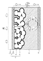
上記のような見地から、最近では、シリコン以外の材料を用いた太陽電池として、色素増感型太陽電池が注目されている。この色素増感型太陽電池は、図1に示すように、透明ガラスや透明樹脂フィルムなどの透明基板1a上に透明導電膜1b(例えばITO膜)を電極基板1として使用し、この電極基板1の透明導電膜1b上に二酸化チタンなどの金属酸化物半導体の多孔質層3を設け、この多孔質層3の表面に増感色素(例えばRu色素)5を吸着させたものを負極7として有しており、このような負極7を、電解質液8を間に挟んで正極10に対峙させた構造を有している。
From the above viewpoint, recently, a dye-sensitized solar cell has attracted attention as a solar cell using a material other than silicon. As shown in FIG. 1, this dye-sensitized solar cell uses a transparent
このような構造の色素増感型太陽電池では、負極7側から可視光を照射すると、色素5が励起され、基底状態から励起状態へと遷移し、励起された色素5の電子は、半導体の多孔質層3の伝導帯へ注入され、外部回路12を通って正極10に移動する。正極10に移動した電子は、電解液中のイオンによって運ばれ、色素5に戻る。このような過程の繰り返しにより電気エネルギーが取り出されるわけである。このような色素増感型太陽電池の発電メカニズムは、pn接合型光電変換素子と異なり、光の捕捉と電子伝導が別々の場所で行われ、植物の光電変換プロセスに非常に似たものとなっている。
In the dye-sensitized solar cell having such a structure, when visible light is irradiated from the
ところで、上記のような色素増感型太陽電池の負極7は、透明基板1aの透明導電膜1b上に、例えば酸化チタンなどの半導体粒子のペーストを塗布し、焼成して酸化チタンからなる半導体の多孔質層3を形成し、この上に色素溶液を塗布し、色素を多孔質層3に吸着させた後、色素溶液の溶媒を除去することにより製造されている(特許文献1参照)。
また、酸化チタン半導体の多孔質層をゾル−ゲル法により形成する方法も知られている(特許文献2,3)。
A method of forming a porous layer of a titanium oxide semiconductor by a sol-gel method is also known (Patent Documents 2 and 3).
しかしながら、上記のような方法で負極を製造する場合には、半導体多孔質層を形成するための焼成を高温で行わなければならないという問題があった。例えば、特許文献1では、水を溶媒として用いて半導体ペーストを調製しているため、可及的に低温で焼成を行ったとしても焼成温度は100℃以上でなければならない。また、特許文献2,3のゾル−ゲル法では、チタンアルコキシドを加水分解して焼成を行うため、やはり水を除去するため、少なくとも焼成温度は100℃以上で無ければならない。実際、特許文献1〜3の何れにおいても、その実施例では焼成が450℃〜約500℃で行われている。従って、このような高温で焼成を行うため、透明電極層を支持する透明基板として樹脂を用いた場合には、焼成時に変形等の不都合を生じ易いという問題があり、樹脂製基板の実用化が妨げられていた。
However, when manufacturing a negative electrode by the above methods, there was a problem that firing for forming a semiconductor porous layer had to be performed at a high temperature. For example, in Patent Document 1, since a semiconductor paste is prepared using water as a solvent, the firing temperature must be 100 ° C. or higher even if firing is performed at as low a temperature as possible. Further, in the sol-gel method of
従って、本発明の目的は、色素増感型の負極における半導体多孔質層形成材料として使用され、100℃未満の低温での焼成で多孔質層を形成することが可能な半導体微粒子ペーストを提供することにある。
本発明の他の目的は、上記の半導体微粒子ペーストを用いて透明電極基板上に半導体多孔質層を形成する方法を提供することにある。
Accordingly, an object of the present invention is to provide a semiconductor fine particle paste that can be used as a material for forming a semiconductor porous layer in a dye-sensitized negative electrode and that can be formed by firing at a low temperature of less than 100 ° C. There is.
Another object of the present invention is to provide a method for forming a semiconductor porous layer on a transparent electrode substrate using the semiconductor fine particle paste.
本発明によれば、二酸化チタン微粒子とテトライソプロポキシチタンと有機溶媒とからなり、該テトライソプロポキシチタンを二酸化チタン微粒子100重量部当り10乃至40重量部の量で含有し、且つ固形分濃度が25乃至50重量%の範囲にあると共に、前記有機溶媒としてブタノールが使用されていることを特徴とする半導体微粒子ペーストが提供される。
本発明によれば、また、上記の半導体微粒子ペーストを、透明電極基板の表面に塗布し、100℃未満の温度で焼成することにより透明電極基板の表面に半導体多孔質層を形成する方法が提供される。
According to the present invention, it comprises titanium dioxide fine particles, tetraisopropoxy titanium and an organic solvent, the tetraisopropoxy titanium is contained in an amount of 10 to 40 parts by weight per 100 parts by weight of titanium dioxide fine particles, and the solid content concentration is There is provided a semiconductor fine particle paste characterized by being in the range of 25 to 50% by weight and using butanol as the organic solvent .
According to the present invention, there is also provided a method for forming a semiconductor porous layer on the surface of a transparent electrode substrate by applying the semiconductor fine particle paste to the surface of the transparent electrode substrate and firing at a temperature of less than 100 ° C. Is done.
本発明においては、
(1)二酸化チタン微粒子が5〜500nmの範囲にあること、
が好ましい。
In the present invention,
(1) The titanium dioxide fine particles are in the range of 5 to 500 nm ,
Is preferred.
本発明の半導体微粒子ペーストは、水を全く含有していない非水系で調製されるため、多孔質化のための焼成を100℃未満の低温領域で行うことが可能となる。また、半導体微粒子ペースト中のテトライソプロポキシチタンは、分散剤的な機能を有し、二酸化チタン微粒子を有機溶媒中に均一に分散させる。この場合、このテトライソプロポキシチタンは、焼成時に容易に酸化されて酸化チタンを形成するため、かかる成分を分解除去するために焼成を高温で行う必要はなく、100℃未満での焼成を妨げない。 Since the semiconductor fine particle paste of the present invention is prepared in a non-aqueous system that does not contain water at all, it is possible to perform firing for porous formation in a low temperature region of less than 100 ° C. Further, tetraisopropoxy titanium in the semiconductor fine particle paste has a function as a dispersant, and the titanium dioxide fine particles are uniformly dispersed in the organic solvent. In this case, since this tetraisopropoxy titanium is easily oxidized at the time of firing to form titanium oxide, it is not necessary to perform firing at a high temperature in order to decompose and remove such components, and does not prevent firing at less than 100 ° C. .
このように、本発明の半導体微粒子ペーストを用いれば、100℃未満の低温での焼成により半導体多孔質層を形成することができるため、透明電極層を支持する透明基板として樹脂を有効に使用することが可能となる。 Thus, if the semiconductor fine particle paste of the present invention is used, the semiconductor porous layer can be formed by firing at a low temperature of less than 100 ° C., so that the resin is effectively used as a transparent substrate for supporting the transparent electrode layer. It becomes possible.
本発明の半導体微粒子ペーストは、二酸化チタンを半導体として使用するものであり、この二酸化チタン微粒子を有機溶媒に分散させたものである。二酸化チタン微粒子は、表面積が大きく、多孔質の層を形成させるという点で、その粒径が5〜500nm、特に5〜350nmの範囲にあるのがよい。 The semiconductor fine particle paste of the present invention uses titanium dioxide as a semiconductor, and the titanium dioxide fine particles are dispersed in an organic solvent. The titanium dioxide fine particles preferably have a large surface area and have a particle size in the range of 5 to 500 nm, particularly 5 to 350 nm in that a porous layer is formed.
また、二酸化チタン微粒子を分散させる有機溶媒としては、ブタノール、例えば、n−ブタノール、sec−ブタノール、t−ブタノールなどが単独または2種以上の組み合わせで使用される。これらは易揮発性であり、低温で容易に揮発して除去できるばかりか、二酸化チタン微粒子に対する分散性が優れているからである。 Moreover, as an organic solvent in which the titanium dioxide fine particles are dispersed, butanol, for example, n-butanol, sec-butanol, t-butanol or the like is used alone or in combination of two or more . This is because they are easily volatile and can be easily volatilized and removed at a low temperature and have excellent dispersibility in titanium dioxide fine particles.
さらに、上記の半導体微粒子ペースト中には、二酸化チタン微粒子100重量部当り、10乃至40重量部、特に10乃至30重量部の量でテトライソプロポキシチタンTi(OPri)4(Pri:イソプロポキシ基)を含有する。先に述べたとおり、テトライソプロポキシチタンは、所謂分散剤としての機能を有しており、有機溶媒(特に前記低級アルコール)中に金属酸化物半導体粒子を均一且つ安定に分散させることができ、更に、半導体粒子同士を連結させるように硬化し、均一な半導体多孔質層を形成するのに有利となる。しかも、テトライソプロポキシチタンは、後述する多孔質化のための焼成によって容易に対応する酸化チタンを形成するため、焼成時にかかる成分を除去する必要はなく、従って焼成温度の高温化をもたらすものではない。 Further, in the semiconductor fine particle paste, tetraisopropoxy titanium Ti (OPr i ) 4 (P r i : isopropoxy) is used in an amount of 10 to 40 parts by weight, particularly 10 to 30 parts by weight per 100 parts by weight of titanium dioxide fine particles. Group). As described above, tetraisopropoxy titanium has a function as a so-called dispersant, and can uniformly and stably disperse metal oxide semiconductor particles in an organic solvent (particularly, the lower alcohol), Furthermore, it hardens | cures so that semiconductor particles may be connected, and it becomes advantageous to form a uniform semiconductor porous layer. Moreover, tetraisopropoxy titanium easily forms the corresponding titanium oxide by firing for porous formation described later, so that it is not necessary to remove such components at the time of firing, so that the firing temperature is increased. Absent.
また、テトライソプロポキシチタンが上記範囲よりも多量に使用されると、分散効果は上昇せず、かえって太陽電池としたときの変換効率を低下する等の不都合を生じ易く、また、上記範囲よりも少量とすると、所望の分散効果を得ることができず、均質な二酸化チタン多孔質層(以下、チタニア多孔質層と呼ぶ)を形成することが困難となってしまう。 Further, when tetraisopropoxy titanium is used in a larger amount than the above range, the dispersion effect does not increase, but it tends to cause inconveniences such as lowering the conversion efficiency when used as a solar cell, and more than the above range. If the amount is small, a desired dispersion effect cannot be obtained, and it becomes difficult to form a homogeneous titanium dioxide porous layer (hereinafter referred to as a titania porous layer).
さらに、上述した半導体微粒子ペーストの固形分濃度は、20乃至50重量%、特に25乃至30重量%の範囲にあるべきである。溶媒量が多すぎると、ペーストが低粘性となり、垂れ等により安定な厚みのコーティング層を形成することが困難となり、また、溶媒量が少ないと、ペーストが高粘性となり作業性が低下してしまう。 Further, the solid content concentration of the above-mentioned semiconductor fine particle paste should be in the range of 20 to 50% by weight, particularly 25 to 30% by weight. If the amount of the solvent is too large, the paste becomes low-viscosity and it becomes difficult to form a coating layer having a stable thickness due to dripping or the like, and if the amount of the solvent is small, the paste becomes high-viscosity and the workability is lowered. .
尚、上述した本発明の半導体微粒子ペーストは、1〜3モル程度のテトライソプロポキシチタンを含有する有機溶媒溶液を調製し、この有機溶媒溶液を二酸化チタン微粒子とともに前述した有機溶媒(即ち、ブタノール)に分散させることにより調製される。
In addition, the semiconductor fine particle paste of the present invention described above prepares an organic solvent solution containing about 1 to 3 moles of tetraisopropoxytitanium, and the organic solvent solution is combined with the titanium dioxide fine particles and the above-mentioned organic solvent (that is, butanol). It is prepared by dispersing in
上述した本発明の半導体微粒ペーストは、非水系で調製され、水を実質上含有しておらず、しかも除去すべき格別の分散剤を含有していないため、多孔質化のための焼成を低温、特に100℃未満で行うことができ、特に樹脂フィルムなどを用いた透明電極基板を有する色素増感型電池の負極の製造に好適に使用される。 The semiconductor fine particle paste of the present invention described above is prepared in a non-aqueous system, does not substantially contain water, and does not contain a special dispersant to be removed. In particular, it can be carried out at a temperature of less than 100 ° C., and is particularly suitably used for producing a negative electrode of a dye-sensitized battery having a transparent electrode substrate using a resin film or the like.
以下、本発明の半導体微粒子ペーストを用いての色素増感型太陽電池における負極の製造プロセスを、図1を参照して説明する。 Hereinafter, the manufacturing process of the negative electrode in the dye-sensitized solar cell using the semiconductor fine particle paste of the present invention will be described with reference to FIG.
先ず、図1で示されている透明電極基板1を用意する。この透明電極基板1は、透明基板1a上に透明導電膜1bを設けたものであり、透明基板1aとしては、透明なガラス板や透明樹脂フィルムが使用される。透明樹脂フィルムとしては、透明である限り任意のものが使用されるが、例えば、低密度ポリエチレン、高密度ポリエチレン、ポリプロピレン、ポリ1−ブテン、ポリ4−メチル−1−ペンテン、或いはエチレン、プロピレン、1−ブテン、4−メチル−1−ペンテン等のα−オレフィン同士のランダム乃至ブロック共重合体等のポリオレフィン系樹脂;エチレン−酢酸ビニル共重合体、エチレン−ビニルアルコール共重合体、エチレン−塩化ビニル共重合体等のエチレン−ビニル化合物共重合体樹脂;ポリスチレン、アクリロニトリル−スチレン共重合体、ABS、α−メチルスチレン−スチレン共重合体等のスチレン系樹脂;ポリビニルアルコール、ポリビニルピロリドン、ポリ塩化ビニル、ポリ塩化ビニリデン、塩化ビニル−塩化ビニリデン共重合体、ポリアクリル酸、ポリメタクリル酸、ポリアクリル酸メチル、ポリメタクリル酸メチル等のビニル系樹脂;ナイロン6、ナイロン6−6、ナイロン6−10、ナイロン11、ナイロン12等のポリアミド樹脂;ポリエチレンテレフタレート、ポリブチレンテレフタレート等のポリエステル樹脂;ポリカーボネート;ポリフェニレンオキサイド;カルボキシメチルセルロース、ヒドロキシエチルセルロースなどのセルロース誘導体;酸化澱粉、エーテル化澱粉、デキストリンなどの澱粉;及びこれらの混合物からなる樹脂;などからなるフィルムを用いることができる。一般的には、強度や耐熱性等の見地から、ポリエチレンテレフタレートフィルムが好適に使用される。また、透明基板1aの厚みや大きさは、特に制限されず、最終的に使用される色素増感型太陽電池の用途に応じて適宜決定される。
First, the transparent electrode substrate 1 shown in FIG. 1 is prepared. This transparent electrode substrate 1 is obtained by providing a transparent
透明導電膜1bとしては、酸化インジウム−酸化錫合金からなる膜(ITO膜)や酸化錫にフッ素をドープした膜(FTO膜)が代表的であるが、電気抵抗が低いことから、特にITO膜が好適である。これらは蒸着により上記の透明基板1a上に形成され、その厚みは、通常、0.5乃至0.7μm程度である。
The transparent
次いで、透明基板1の透明導電膜1b上に、前述した本発明の半導体粒子ペーストを塗布する。このペースト層は、焼成により図1における半導体多孔質層(チタニア多孔質層)3を形成するものである。
Next, the above-described semiconductor particle paste of the present invention is applied onto the transparent
半導体微粒子ペーストのコーティングは、ドクターブレード法、スピンコート法、スクリーン印刷法、スプレーコーティング法等の周知の方法で行うことができ、その厚みは、焼成後の厚みが5乃至20μm程度、半導体重量としては、0.001乃至0.005g/cm2程度となるようにするのがよい。 The coating of the semiconductor fine particle paste can be performed by a known method such as a doctor blade method, a spin coating method, a screen printing method, a spray coating method, and the thickness thereof is about 5 to 20 μm after firing, Is preferably about 0.001 to 0.005 g / cm 2 .
上記のようにして本発明の半導体微粒子ペーストを透明基板1の透明導電膜1b上にコーティングした後に、焼成を行う。この焼成は、既に述べたように、100℃未満、特に70乃至95℃の温度で行うことができ、これにより、チタニア多孔質層3が形成される。即ち、このような低温領域で焼成を行うことができるため、前述した透明ガラスは、勿論のこと、透明な樹脂フィルムを透明基板1aとして用いた場合にも、焼成時の変形を防止することができ、樹脂フィルムも基板材料として好適に使用することが可能となる。また、この焼成は、ペースト中の金属酸化物粒子が適度に焼結する程度でよく、例えばアルキメデス法による相対密度が50乃至90%に達する程度に緻密化されていればよく、通常、大気中で5乃至30分程度行えばよい。
After coating the semiconductor fine particle paste of the present invention on the transparent
上記のようにして形成されたチタニア多孔質層3に色素溶液を接触させることにより、増感色素5を吸着させる。色素溶液の接触は、通常は、ディッピングにより行われ、吸着処理時間(浸漬時間)は、通常、30分〜24時間程度であり、吸着後、乾燥して色素溶液の溶媒を除去することにより、表面に増感色素5が形成された半導体多孔質層3を有する負極7を得ることができる。
The sensitizing dye 5 is adsorbed by bringing the dye solution into contact with the titania
用いる増感色素は、カルボキシレート基、シアノ基、ホスフェート基、オキシム基、ジオキシム基、ヒドロキシキノリン基、サリチレート基、α−ケト−エノール基などの結合基を有するそれ自体公知のものが使用され、前述した特許文献1〜3等に記載されているもの、例えばルテニウム錯体、オスミウム錯体、鉄錯体などを何ら制限なく使用することができる。特に幅広い吸収帯を有するなどの点で、ルテニウム−トリス(2,2’−ビスピリジル−4,4’−ジカルボキシラート)、ルテニウム−シス−ジアクア−ビス(2,2’−ビスピリジル−4,4’−ジカルボキシラート)などのルテニウム系錯体が好適である。このような増感色素の色素溶液は、溶媒としてエタノールやブタノールなどのアルコール系有機溶媒を用いて調製され、その色素濃度は、通常、3×10⁻⁴乃至5×10⁻⁴mol/l程度である。 As the sensitizing dye to be used, those known per se having a linking group such as a carboxylate group, a cyano group, a phosphate group, an oxime group, a dioxime group, a hydroxyquinoline group, a salicylate group, an α-keto-enol group are used. Those described in Patent Documents 1 to 3 described above, for example, ruthenium complexes, osmium complexes, iron complexes, and the like can be used without any limitation. Ruthenium-tris (2,2′-bispyridyl-4,4′-dicarboxylate), ruthenium-cis-diaqua-bis (2,2′-bispyridyl-4,4) in that it has a particularly broad absorption band. Ruthenium-based complexes such as' -dicarboxylate) are preferred. Such a dye solution of a sensitizing dye is prepared using an alcohol organic solvent such as ethanol or butanol as a solvent, and the dye concentration is usually about 3 × 10 −4 to 5 × 10 −4 mol / l. It is.
また、上記の製造プロセスでは、本発明の半導体微粒子ペーストをコーティングし、焼成を行った後に色素の吸着を行っているが、本発明の半導体微粒子ペーストを用いると、100℃未満の低温領域で焼成を行うことができるため、焼成を色素の吸着処理を行った後に行うこともできる。即ち、半導体微粒子ペーストを塗布し、乾燥を行った後に、ディッピング等により色素溶液を接触させて増感色素を吸着させ、この後に、焼成を行うことも可能である。この場合の乾燥は、大気中に放置するのみでの自然乾燥でよいが、必要により、100℃未満の温度に加熱してもよい。 In the manufacturing process described above, the semiconductor fine particle paste of the present invention is coated and the dye is adsorbed after firing. However, when the semiconductor fine particle paste of the present invention is used, firing is performed in a low temperature region of less than 100 ° C. Therefore, the baking can be performed after the dye adsorption treatment. That is, after the semiconductor fine particle paste is applied and dried, the dye solution is brought into contact by dipping or the like to adsorb the sensitizing dye, and then baked. The drying in this case may be natural drying simply by leaving it in the atmosphere, but may be heated to a temperature of less than 100 ° C. if necessary.
上記のように、色素の吸着を焼成に先立って行う場合には、ペースト中の半導体微粒子(二酸化チタン微粒子)が焼結しておらず、ばらばらの状態で存在しているため、吸着処理を短時間で行うことができるという大きな利点がある。即ち、色素溶液が迅速に半導体微粒子中に浸透し、増感色素の吸着が速やかに行われ、例えば、10〜15分程度の短時間で吸着処理を行うことができ、焼成後に吸着処理を行う場合の1/2以下の時間で吸着処理を完了することが可能となり、生産性、量産性の点で極めて優れている。 As described above, when the adsorption of the dye is performed prior to firing, the semiconductor fine particles (titanium dioxide fine particles) in the paste are not sintered and exist in a discrete state, so that the adsorption treatment is short. The great advantage is that it can be done in time. That is, the dye solution quickly penetrates into the semiconductor fine particles, and the adsorption of the sensitizing dye is performed quickly. For example, the adsorption process can be performed in a short time of about 10 to 15 minutes, and the adsorption process is performed after firing. The adsorption process can be completed in half the time or less, which is extremely excellent in terms of productivity and mass productivity.
上記のようにして得られた負極7は、図1に示すように、電解質液8を間に挟んで対極である正極10に対峙させることにより、色素増感型太陽電池として使用に供される。
As shown in FIG. 1, the
尚、電解質液8としては、通常、リチウムイオン等の陽イオンや塩素イオン等の陰イオンを含む種々の電解質溶液を使用することができる。また、この電解質溶液中には、酸化型構造及び還元型構造を可逆的にとり得るような酸化還元対を存在させることが好ましく、このような酸化還元対としては、例えばヨウ素−ヨウ素化合物、臭素−臭素化合物、キノン−ヒドロキノンなどを挙げることができる。また、この電解質液8は、一般に、電気絶縁性の樹脂等により封止され、電極間から漏洩しないように構成されている。
As the
また、正極10は、透明、不透明に関係なく、種々の電極基板を用いることができ、例えばガラス基板や透明樹脂フィルムなどの透明基板表面に白金層やITO等の透明電極層を蒸着させたもの、或いは透明基板表面にITO等の透明電極層を蒸着させ、さらにその上に白金層を蒸着させたものなど、任意の構造を採ることができる。
In addition, the
チタンイソプロポキシドを2mol/Lになるように、有機溶剤ブタノールで希釈したチタンアルコキシド溶液を調製し、この溶液と二酸化チタン粒子(構成粒子径は、15〜350nmの汎用チタニア粒子)とを混合し、二酸化チタン微粒子100重量部当り20重量部の量でチタンイソプロポキシドを含有し、且つ固形分濃度が30重量%の二酸化チタン微粒子ペーストを調製した。 Prepare titanium alkoxide solution diluted with organic solvent butanol so that titanium isopropoxide is 2 mol / L, and mix this solution with titanium dioxide particles (general-purpose titania particles with a component particle size of 15 to 350 nm). A titanium dioxide fine particle paste containing titanium isopropoxide in an amount of 20 parts by weight per 100 parts by weight of titanium dioxide fine particles and having a solid content concentration of 30% by weight was prepared.
そして、ポリエチレンテレフタレートフィルムに導電膜としてITO膜を設けた導電性フィルム(トービ社製、製品名「OTEC」)に、上記で調製した二酸化チタンのペーストを塗布し、その後、室温での大気放置にて、5分間乾燥を行った。乾燥後の半導体ペースト(半導体コーティング層)の厚みは約5μmで、半導体重量は約0.002g/cm2であった。 Then, the titanium dioxide paste prepared above is applied to a conductive film (product name “OTEC”, manufactured by Tobi Co., Ltd.) in which an ITO film is provided as a conductive film on a polyethylene terephthalate film, and then left in the atmosphere at room temperature. And dried for 5 minutes. The thickness of the dried semiconductor paste (semiconductor coating layer) was about 5 μm, and the semiconductor weight was about 0.002 g / cm 2 .
その後、純度99.5%のエタノールに分散させたルテニウム錯体色素[Ru(dcbpy)2(NCS)2]・2H2Oからなる色素溶液を、ITO膜上に形成された半導体コーティング層(チタニア膜)上に滴下・吸着し(吸着時間10分)、大気雰囲気の電気オーブンで70℃×10分の条件で焼成を行って、負極を得た。 Thereafter, a semiconductor coating layer (titania film) formed on the ITO film by a dye solution composed of a ruthenium complex dye [Ru (dcbpy) 2 (NCS) 2 ] · 2H 2 O dispersed in ethanol having a purity of 99.5% ) Was dropped and adsorbed onto the substrate (adsorption time: 10 minutes), and baked under conditions of 70 ° C. × 10 minutes in an electric oven in an air atmosphere to obtain a negative electrode.
以上のようにして得られた負極を用い、LiI/I2 (0.5mol/0.05mol)をメトキシプロピオニトリルに溶かしたものに4-tert-butyl pyridine(ターシャリーブチルピリジン)を添加して作製した電解質を、白金を蒸着したITO/PETフィルムで構成される正極と上記負極とで挟み込んで、色素増感型太陽電池を作成した。この電池の変換効率を測定したところ、約3%であり、太陽電池として機能することが確認された。 Using the negative electrode obtained as described above, 4-tert-butyl pyridine was added to LiI / I 2 (0.5 mol / 0.05 mol) dissolved in methoxypropionitrile. The obtained electrolyte was sandwiched between a positive electrode composed of an ITO / PET film on which platinum was deposited and the negative electrode to prepare a dye-sensitized solar cell. When the conversion efficiency of this battery was measured, it was about 3%, and it was confirmed that it functions as a solar battery.
実施例1で調製されたチタンアルコキシド溶液を使用し、実施例1と同様にして、二酸化チタン微粒子100重量部当り10重量部の量でチタンイソプロポキシドを含有し、且つ固形分濃度が45重量%の二酸化チタン微粒子ペーストを調製した。 The titanium alkoxide solution prepared in Example 1 was used, and in the same manner as in Example 1, titanium isopropoxide was contained in an amount of 10 parts by weight per 100 parts by weight of titanium dioxide fine particles, and the solid content concentration was 45% by weight. % Titanium dioxide fine particle paste was prepared.
そして、上記で調製された二酸化チタン微粒子ペーストを用いて、実施例1と同様の導電性フィルムに塗布し、その後、室温での大気放置にて、5分間乾燥を行った。乾燥後の半導体ペースト(半導体コーティング層)の厚みは約5μmで、半導体重量は約0.003g/cm2であった。 And using the titanium dioxide fine particle paste prepared above, it apply | coated to the electroconductive film similar to Example 1, and dried for 5 minutes by leaving to air | atmosphere at room temperature after that. The dried semiconductor paste (semiconductor coating layer) had a thickness of about 5 μm and a semiconductor weight of about 0.003 g / cm 2 .
その後、実施例1と同様に、色素溶液を、ITO膜上の半導体コーティング層(チタニア膜)上に滴下・吸着し(吸着時間10分)、大気雰囲気の電気オーブンで70℃×10分の条件で焼成を行って、負極を得た。
Thereafter, in the same manner as in Example 1, the dye solution was dropped and adsorbed onto the semiconductor coating layer (titania film) on the ITO film (
以上のようにして得られた負極を用い、実施例1と同様にして、該負極と正極との間に電解質を挟み込んだ色素増感型太陽電池を作成した。この電池の変換効率を測定したところ、約2%であり、太陽電池として機能することが確認された。 Using the negative electrode obtained as described above, a dye-sensitized solar cell in which an electrolyte was sandwiched between the negative electrode and the positive electrode was produced in the same manner as in Example 1. When the conversion efficiency of this battery was measured, it was about 2%, and it was confirmed that it functions as a solar battery.
実施例1で調製されたチタンアルコキシド溶液を使用し、実施例1と同様にして、二酸化チタン微粒子100重量部当り40重量部の量でチタンイソプロポキシドを含有し、且つ固形分濃度が30重量%の二酸化チタン微粒子ペーストを調製した。 Using the titanium alkoxide solution prepared in Example 1, in the same manner as in Example 1, titanium isopropoxide was contained in an amount of 40 parts by weight per 100 parts by weight of titanium dioxide fine particles, and the solid content concentration was 30% by weight. % Titanium dioxide fine particle paste was prepared.
そして、上記で調製された二酸化チタン微粒子ペーストを用いて、実施例1と同様の導電性フィルムに塗布し、その後、室温での大気放置にて、5分間乾燥を行った。乾燥後の半導体ペースト(半導体コーティング層)の厚みは約5μmで、半導体重量は約0.002g/cm2であった。 And using the titanium dioxide fine particle paste prepared above, it apply | coated to the electroconductive film similar to Example 1, and dried for 5 minutes by leaving to air | atmosphere at room temperature after that. The thickness of the dried semiconductor paste (semiconductor coating layer) was about 5 μm, and the semiconductor weight was about 0.002 g / cm 2 .
その後、実施例1と同様に、色素溶液を、ITO膜上の半導体コーティング層(チタニア膜)上に滴下・吸着し(吸着時間10分)、大気雰囲気の電気オーブンで70℃×10分の条件で焼成を行って、負極を得た。
Thereafter, in the same manner as in Example 1, the dye solution was dropped and adsorbed onto the semiconductor coating layer (titania film) on the ITO film (
以上のようにして得られた負極を用い、実施例1と同様にして、該負極と正極との間に電解質を挟み込んだ色素増感型太陽電池を作成した。この電池の変換効率を測定したところ、約2%であり、太陽電池として機能することが確認された。 Using the negative electrode obtained as described above, a dye-sensitized solar cell in which an electrolyte was sandwiched between the negative electrode and the positive electrode was produced in the same manner as in Example 1. When the conversion efficiency of this battery was measured, it was about 2%, and it was confirmed that it functions as a solar battery.
(比較例1)
実施例1で調製されたチタンアルコキシド溶液を使用し、実施例1と同様にして、二酸化チタン微粒子100重量部当り20重量部の量でチタンイソプロポキシドを含有し、且つ固形分濃度が55重量%の二酸化チタン微粒子ペーストを調製した。
(Comparative Example 1)
The titanium alkoxide solution prepared in Example 1 was used, and in the same manner as in Example 1, titanium isopropoxide was contained in an amount of 20 parts by weight per 100 parts by weight of titanium dioxide fine particles, and the solid content concentration was 55% by weight. % Titanium dioxide fine particle paste was prepared.
そして、上記で調製された二酸化チタン微粒子ペーストを用いて、実施例1と同様の導電性フィルムに塗布し、その後、室温での大気放置にて、5分間乾燥を行った。乾燥後の半導体ペースト(半導体コーティング層)の厚みは約5μmで、半導体重量は約0.002g/cm2であった。 And using the titanium dioxide fine particle paste prepared above, it apply | coated to the electroconductive film similar to Example 1, and dried for 5 minutes by leaving to air | atmosphere at room temperature after that. The thickness of the dried semiconductor paste (semiconductor coating layer) was about 5 μm, and the semiconductor weight was about 0.002 g / cm 2 .
その後、実施例1と同様に、色素溶液を、ITO膜上の半導体コーティング層(チタニア膜)上に滴下・吸着し(吸着時間10分)、大気雰囲気の電気オーブンで70℃×10分の条件で焼成を行って、負極を得た。
Thereafter, in the same manner as in Example 1, the dye solution was dropped and adsorbed onto the semiconductor coating layer (titania film) on the ITO film (
以上のようにして得られた負極を用い、実施例1と同様にして、該負極と正極との間に電解質を挟み込んだ色素増感型太陽電池を作成した。この電池の変換効率を測定したところ、殆ど機能しておらず、機能しない原因は、負極の二酸化チタンの分散が不十分であったためである。 Using the negative electrode obtained as described above, a dye-sensitized solar cell in which an electrolyte was sandwiched between the negative electrode and the positive electrode was produced in the same manner as in Example 1. When the conversion efficiency of this battery was measured, it hardly functioned, and the reason why it did not function was that titanium dioxide in the negative electrode was not sufficiently dispersed.
(比較例2)
実施例1で調製されたチタンアルコキシド溶液を使用し、実施例1と同様にして、二酸化チタン微粒子100重量部当り5重量部の量でチタンイソプロポキシドを含有し、且つ固形分濃度が25重量%の二酸化チタン微粒子ペーストを調製した。
(Comparative Example 2)
The titanium alkoxide solution prepared in Example 1 was used, and in the same manner as in Example 1, titanium isopropoxide was contained in an amount of 5 parts by weight per 100 parts by weight of titanium dioxide fine particles, and the solid content concentration was 25% by weight. % Titanium dioxide fine particle paste was prepared.
そして、上記で調製された二酸化チタン微粒子ペーストを用いて、実施例1と同様の導電性フィルムに塗布し、その後、室温での大気放置にて、5分間乾燥を行った。乾燥後の半導体ペースト(半導体コーティング層)の厚みは約5μmで、半導体重量は約0.002g/cm2であった。 And using the titanium dioxide fine particle paste prepared above, it apply | coated to the electroconductive film similar to Example 1, and dried for 5 minutes by leaving to air | atmosphere at room temperature after that. The thickness of the dried semiconductor paste (semiconductor coating layer) was about 5 μm, and the semiconductor weight was about 0.002 g / cm 2 .
その後、実施例1と同様に、色素溶液を、ITO膜上の半導体コーティング層(チタニア膜)上に滴下・吸着し(吸着時間10分)、大気雰囲気の電気オーブンで70℃×10分の条件で焼成を行って、負極を得た。
Thereafter, in the same manner as in Example 1, the dye solution was dropped and adsorbed onto the semiconductor coating layer (titania film) on the ITO film (
以上のようにして得られた負極を用い、実施例1と同様にして、該負極と正極との間に電解質を挟み込んだ色素増感型太陽電池を作成した。この電池の変換効率を測定したところ、殆ど機能しておらず、機能しない原因は、比較例1と同様、負極の二酸化チタンの分散が不十分であったためである。 Using the negative electrode obtained as described above, a dye-sensitized solar cell in which an electrolyte was sandwiched between the negative electrode and the positive electrode was produced in the same manner as in Example 1. When the conversion efficiency of this battery was measured, it was hardly functioning and the reason why it did not function was that, as in Comparative Example 1, the titanium dioxide in the negative electrode was not sufficiently dispersed.
(比較例3)
実施例1で調製されたチタンアルコキシド溶液を使用し、実施例1と同様にして、二酸化チタン微粒子100重量部当り40重量部の量でチタンイソプロポキシドを含有し、且つ固形分濃度が20重量%の二酸化チタン微粒子ペーストを調製した。
(Comparative Example 3)
Using the titanium alkoxide solution prepared in Example 1, in the same manner as in Example 1, titanium isopropoxide was contained in an amount of 40 parts by weight per 100 parts by weight of titanium dioxide fine particles, and the solid content concentration was 20% by weight. % Titanium dioxide fine particle paste was prepared.
そして、上記で調製された二酸化チタン微粒子ペーストを用いて、実施例1と同様の導電性フィルムに塗布し、その後、室温での大気放置にて、5分間乾燥を行った。乾燥後の半導体ペースト(半導体コーティング層)の厚みは約3μmで、半導体重量は約0.01g/cm2であった。 And using the titanium dioxide fine particle paste prepared above, it apply | coated to the electroconductive film similar to Example 1, and dried for 5 minutes by leaving to air | atmosphere at room temperature after that. The dried semiconductor paste (semiconductor coating layer) had a thickness of about 3 μm and a semiconductor weight of about 0.01 g / cm 2 .
その後、実施例1と同様に、色素溶液を、ITO膜上の半導体コーティング層(チタニア膜)上に滴下・吸着し(吸着時間10分)、大気雰囲気の電気オーブンで70℃×10分の条件で焼成を行って、負極を得た。
Thereafter, in the same manner as in Example 1, the dye solution was dropped and adsorbed onto the semiconductor coating layer (titania film) on the ITO film (
以上のようにして得られた負極を用い、実施例1と同様にして、該負極と正極との間に電解質を挟み込んだ色素増感型太陽電池を作成した。この電池の変換効率を測定したところ、殆ど機能しておらず、機能しない原因は、負極の二酸化チタン多孔質層を3μm以上の厚みに厚膜化できなかったためである。 Using the negative electrode obtained as described above, a dye-sensitized solar cell in which an electrolyte was sandwiched between the negative electrode and the positive electrode was produced in the same manner as in Example 1. When the conversion efficiency of this battery was measured, it hardly functioned, and the reason why it did not function was that the titanium dioxide porous layer of the negative electrode could not be thickened to 3 μm or more.
(比較例4)
実施例1で調製されたチタンアルコキシド溶液を使用し、実施例1と同様にして、二酸化チタン微粒子100重量部当り50重量部の量でチタンイソプロポキシドを含有し、且つ固形分濃度が30重量%の二酸化チタン微粒子ペーストを調製した。
(Comparative Example 4)
Using the titanium alkoxide solution prepared in Example 1, in the same manner as in Example 1, titanium isopropoxide was contained in an amount of 50 parts by weight per 100 parts by weight of titanium dioxide fine particles, and the solid content concentration was 30% by weight. % Titanium dioxide fine particle paste was prepared.
そして、上記で調製された二酸化チタン微粒子ペーストを用いて、実施例1と同様の導電性フィルムに塗布し、その後、室温での大気放置にて、5分間乾燥を行った。その結果、半導体ペーストのコーティング層に多数の亀裂が入り、焼成による多孔質層の形成ができなくなった。 And using the titanium dioxide fine particle paste prepared above, it apply | coated to the electroconductive film similar to Example 1, and dried for 5 minutes by leaving to air | atmosphere at room temperature after that. As a result, many cracks were formed in the coating layer of the semiconductor paste, and the porous layer could not be formed by firing.
1:透明電極基板
1a:透明基板
1b:透明導電層
3:半導体多孔質層(チタニア多孔質層)
5:増感色素
7:負極
8:電解質液
10:正極
1: Transparent electrode substrate 1a:
5: Sensitizing dye 7: Negative electrode 8: Electrolyte solution 10: Positive electrode
Claims (3)
Priority Applications (1)
| Application Number | Priority Date | Filing Date | Title |
|---|---|---|---|
| JP2004029158A JP4635447B2 (en) | 2004-02-05 | 2004-02-05 | Semiconductor fine particle paste |
Applications Claiming Priority (1)
| Application Number | Priority Date | Filing Date | Title |
|---|---|---|---|
| JP2004029158A JP4635447B2 (en) | 2004-02-05 | 2004-02-05 | Semiconductor fine particle paste |
Publications (2)
| Publication Number | Publication Date |
|---|---|
| JP2005222799A JP2005222799A (en) | 2005-08-18 |
| JP4635447B2 true JP4635447B2 (en) | 2011-02-23 |
Family
ID=34998269
Family Applications (1)
| Application Number | Title | Priority Date | Filing Date |
|---|---|---|---|
| JP2004029158A Expired - Fee Related JP4635447B2 (en) | 2004-02-05 | 2004-02-05 | Semiconductor fine particle paste |
Country Status (1)
| Country | Link |
|---|---|
| JP (1) | JP4635447B2 (en) |
Families Citing this family (2)
| Publication number | Priority date | Publication date | Assignee | Title |
|---|---|---|---|---|
| JP4807020B2 (en) * | 2005-09-21 | 2011-11-02 | 東洋製罐株式会社 | Method for producing binder composition for dispersing semiconductor fine particles |
| JP2007242544A (en) * | 2006-03-10 | 2007-09-20 | Sony Corp | Photoelectric conversion device and method for producing the same, and surface treatment liquid for metal oxide porous layer |
Family Cites Families (5)
| Publication number | Priority date | Publication date | Assignee | Title |
|---|---|---|---|---|
| JP2002075477A (en) * | 2000-08-31 | 2002-03-15 | Tdk Corp | Photoelectric conversion film, photoelectric conversion electrode, and photoelectric conversion element |
| DE60140819D1 (en) * | 2000-11-02 | 2010-01-28 | Asahi Chemical Ind | ALUMINUM PIGMENT COMPOSITION |
| JP5102921B2 (en) * | 2001-03-21 | 2012-12-19 | リンテック株式会社 | Manufacturing method of semiconductor electrode |
| JP3692472B2 (en) * | 2002-03-25 | 2005-09-07 | テイカ株式会社 | Low temperature synthesis of conductive titanium oxide porous thick film |
| JP3671183B2 (en) * | 2003-09-04 | 2005-07-13 | 司 吉田 | Method for producing dye-sensitized solar cell |
-
2004
- 2004-02-05 JP JP2004029158A patent/JP4635447B2/en not_active Expired - Fee Related
Also Published As
| Publication number | Publication date |
|---|---|
| JP2005222799A (en) | 2005-08-18 |
Similar Documents
| Publication | Publication Date | Title |
|---|---|---|
| TW516242B (en) | Photoelectric conversion element | |
| CN101521114A (en) | Preparation method for laminated photo-anode film of dye-sensitized solar cell | |
| US8455295B2 (en) | Low temperature sintering of dye-sensitised solar cells | |
| US20100229949A1 (en) | Dye-sensitized solar cell | |
| KR101470680B1 (en) | Dye-sensitized solar cell and electrode substrate therefor, method of producing an electrode substrate, and paste for forming a semiconductor porous layer | |
| JP5266524B2 (en) | Electrode substrate for dye-sensitized solar cell and dye-sensitized solar cell | |
| JP2005251591A (en) | Manufacturing method of negative electrode in dye-sensitized solar cell | |
| JP2004164950A (en) | Electrode substrate, photoelectric conversion element, and dye-sensitized solar cell | |
| JP4595337B2 (en) | Method for producing negative electrode in dye-sensitized solar cell | |
| JP5332358B2 (en) | Coating solution for reverse electron prevention layer formation | |
| JP4807020B2 (en) | Method for producing binder composition for dispersing semiconductor fine particles | |
| JP2010020938A (en) | Dye-sensitized solar battery | |
| JP5661965B1 (en) | Material for organic solar cell, organic solar cell using the same, and method for producing the material | |
| JP4635447B2 (en) | Semiconductor fine particle paste | |
| JP2009129574A (en) | Dye-sensitized solar cell | |
| JP4608897B2 (en) | Method for producing negative electrode in dye-sensitized solar cell | |
| JP5396757B2 (en) | Coating composition for forming electron reducing layer and method for forming electron reducing layer | |
| JP2008053140A (en) | Semiconductor particulate paste | |
| JP5109308B2 (en) | Dye-sensitized solar cell | |
| JP4904698B2 (en) | Method for producing negative electrode in dye-sensitized solar cell | |
| US20130160843A1 (en) | Ultra-low temperature sintering of dye-sensitesed solar cells | |
| JP2007242544A (en) | Photoelectric conversion device and method for producing the same, and surface treatment liquid for metal oxide porous layer | |
| JP2008152949A (en) | Titanium oxide film, semiconductor electrode, and dye-sensitized solar cell | |
| JP2010080090A (en) | Negative electrode substrate used for pigment sensitized solar battery | |
| JP5286496B2 (en) | Semiconductor porous layer forming paste |
Legal Events
| Date | Code | Title | Description |
|---|---|---|---|
| A621 | Written request for application examination |
Free format text: JAPANESE INTERMEDIATE CODE: A621 Effective date: 20070118 |
|
| A977 | Report on retrieval |
Free format text: JAPANESE INTERMEDIATE CODE: A971007 Effective date: 20090714 |
|
| A131 | Notification of reasons for refusal |
Free format text: JAPANESE INTERMEDIATE CODE: A131 Effective date: 20090728 |
|
| A521 | Request for written amendment filed |
Free format text: JAPANESE INTERMEDIATE CODE: A523 Effective date: 20090918 |
|
| TRDD | Decision of grant or rejection written | ||
| A01 | Written decision to grant a patent or to grant a registration (utility model) |
Free format text: JAPANESE INTERMEDIATE CODE: A01 Effective date: 20101026 |
|
| A01 | Written decision to grant a patent or to grant a registration (utility model) |
Free format text: JAPANESE INTERMEDIATE CODE: A01 |
|
| A61 | First payment of annual fees (during grant procedure) |
Free format text: JAPANESE INTERMEDIATE CODE: A61 Effective date: 20101108 |
|
| FPAY | Renewal fee payment (event date is renewal date of database) |
Free format text: PAYMENT UNTIL: 20131203 Year of fee payment: 3 |
|
| R150 | Certificate of patent or registration of utility model |
Free format text: JAPANESE INTERMEDIATE CODE: R150 |
|
| FPAY | Renewal fee payment (event date is renewal date of database) |
Free format text: PAYMENT UNTIL: 20131203 Year of fee payment: 3 |
|
| S531 | Written request for registration of change of domicile |
Free format text: JAPANESE INTERMEDIATE CODE: R313531 |
|
| FPAY | Renewal fee payment (event date is renewal date of database) |
Free format text: PAYMENT UNTIL: 20131203 Year of fee payment: 3 |
|
| R350 | Written notification of registration of transfer |
Free format text: JAPANESE INTERMEDIATE CODE: R350 |
|
| S533 | Written request for registration of change of name |
Free format text: JAPANESE INTERMEDIATE CODE: R313533 |
|
| FPAY | Renewal fee payment (event date is renewal date of database) |
Free format text: PAYMENT UNTIL: 20131203 Year of fee payment: 3 |
|
| R350 | Written notification of registration of transfer |
Free format text: JAPANESE INTERMEDIATE CODE: R350 |
|
| S111 | Request for change of ownership or part of ownership |
Free format text: JAPANESE INTERMEDIATE CODE: R313111 |
|
| R350 | Written notification of registration of transfer |
Free format text: JAPANESE INTERMEDIATE CODE: R350 |
|
| LAPS | Cancellation because of no payment of annual fees |