JP4635312B2 - Adhesive composition, circuit connection material, adhesive composition for circuit connection, connector and semiconductor device - Google Patents
Adhesive composition, circuit connection material, adhesive composition for circuit connection, connector and semiconductor device Download PDFInfo
- Publication number
- JP4635312B2 JP4635312B2 JP2000286292A JP2000286292A JP4635312B2 JP 4635312 B2 JP4635312 B2 JP 4635312B2 JP 2000286292 A JP2000286292 A JP 2000286292A JP 2000286292 A JP2000286292 A JP 2000286292A JP 4635312 B2 JP4635312 B2 JP 4635312B2
- Authority
- JP
- Japan
- Prior art keywords
- group
- carbon atoms
- adhesive composition
- circuit
- adhesive
- Prior art date
- Legal status (The legal status is an assumption and is not a legal conclusion. Google has not performed a legal analysis and makes no representation as to the accuracy of the status listed.)
- Expired - Fee Related
Links
Images
Landscapes
- Conductive Materials (AREA)
- Adhesive Tapes (AREA)
- Adhesives Or Adhesive Processes (AREA)
- Connections Effected By Soldering, Adhesion, Or Permanent Deformation (AREA)
- Electric Connection Of Electric Components To Printed Circuits (AREA)
- Combinations Of Printed Boards (AREA)
- Wire Bonding (AREA)
Description
【0001】
【発明の属する技術分野】
本発明は、接着剤組成物、回路接続材料、回路接続用接着剤組成物、接続体及び半導体装置に関する。
【0002】
【従来の技術】
半導体素子及び液晶表示素子において、素子中の種々の部材を結合させる目的で従来から種々の接着剤が使用されている。接着剤に対する要求は、接着性をはじめとして、耐熱性、高温高湿状態における信頼性等多岐に渡る特性が要求されている。また、接着に使用される被着体は、プリント配線板やポリイミド等の有機基材をはじめ、銅、アルミニウム等の金属やITO等の無機材質で形成された回路電極面、シリコンウェハ等の多種多様な基材が用いられ、各被着体にあわせた分子設計が必要である。
従来から、前記半導体素子や液晶表示素子用の接着剤としては、高接着性でかつ高信頼性を示すエポキシ樹脂を用いた熱硬化性樹脂が用いられてきた。樹脂の構成成分としては、エポキシ樹脂、エポキシ樹脂と反応性を有するフェノール樹脂等の硬化剤、エポキシ樹脂と硬化剤の反応を促進する熱潜在性触媒が一般に用いられている。熱潜在性触媒は硬化温度及び硬化速度を決定する重要な因子となっており、室温での貯蔵安定性と加熱時の硬化速度の観点から種々の化合物が用いられてきた。実際の工程での硬化条件は、170〜250℃の温度で1〜3時間硬化することにより、所望の接着を得ていた。
また、接着剤を用いた回路電極の接続方法として、2つの回路基板同士を接着すると共に、これらの電極間に電気的導通を得る接着剤として、スチレン系やポリエステル系等の熱可塑性物質や、エポキシ系やシリコーン系等の熱硬化性物質が用いられている。この場合、接着剤中に導電性粒子を配合し加圧により接着剤の厚み方向に電気的接続を得るもの(例えば特開昭55−104007号公報)と、導電性粒子を用いずに接続時の加圧により電極面の微細凸凹の接触により電気的接続を得るもの(例えば特開昭60−262430号公報)とがある。
しかしながら、最近の半導体素子の高集積化、液晶素子の高精細化に伴い、素子間及び配線間ピッチが狭小化し、硬化時の加熱によって、周辺部材に悪影響を及ぼす恐れが出てきた。さらに低コスト化のためには、スループットを向上させる必要性があり、低温(100〜170℃)、短時間(1時間以内、好ましくは数十秒以下)、換言すれば低温速硬化での接着が要求されている。この低温速硬化を達成するためには、活性化エネルギーの低い熱潜在性触媒を使用する必要があるが、この場合、室温付近での貯蔵安定性を兼備することが非常に難しい。
貯蔵安定性及び低温硬化性を兼備えた接着剤として、エポキシ樹脂の光カチオン重合を用いる方法が特開平11−60899号公報及び特開平11−116778号公報に開示されている。これらは、エポキシ樹脂と光照射によって強酸を発生する光酸発生剤から構成されており、室温で光照射することにより硬化を行う方法である。
【0003】
【発明が解決しようとする課題】
しかしながら、前記光カチオン重合の場合、重合触媒としてブレンステッド酸やルイス酸等の強酸を使用するため、被着体である金属基板や金属及び無機材質で構成される回路電極の腐食を促進し、接続体の信頼性を著しく低下させてしまう問題があった。また、接着剤にエポキシ樹脂を用いた場合、エポキシ樹脂中に残存する不純物イオンが、被着体の銅、アルミニウム等の金属やITO等の無機材質で形成される回路電極の腐食を引き起こし、結果的に接続体としての機能を低下させてしまう。
【0004】
本発明は、金属及び無機材質で構成される被着体の腐食に伴う素子の信頼性低下を防ぎ、さらに室温での貯蔵安定性に優れる接着剤組成物、回路接続材料、回路接続用接着剤組成物、接続体及び半導体装置を提供するものである。
【0005】
【課題を解決するための手段】
本発明は、[1](a)150〜750nmの光照射、または80〜200℃の加熱、または光照射と加熱を併用することで硬化する硬化性接着剤、(b)一般式(A)及び/又は一般式(B)で示される化合物とを含有し、(a)硬化性接着剤が、エポキシ樹脂と分子内にフェノール性水酸基、チオール基、カルボキシル基を少なくとも一つ以上有する樹脂と硬化促進剤とを含むもの、又は、カチオン重合性樹脂と熱および/又は光照射よってカチオンを発生する重合開始剤とを含むものであり、(a)硬化性接着剤100重量部に対して、(b)一般式(A)および/または一般式(B)で示される化合物0.5〜30重量部含有する接着剤組成物である。
【化3】
【化4】
また、本発明は、[2]上記[1]に記載の接着剤組成物中に、さらに導電性粒子を含む接着剤組成物である。また、本発明は、[3]上記[1]又は[2]に記載の接着剤組成物の形状をフィルム状とした回路接続材料である。また、本発明は、[4]相対向する回路電極を有する回路部材間に介在させ、相対向する回路電極を有する回路部材を加圧して加圧方向の電極間を電気的に接続する接着剤組成物であって、前記接着剤組成物は、上記[1]ないし上記[3]のいずれかに記載の接着剤組成物または回路接続材料である回路接続用接着剤組成物である。また、本発明は、[5]上記[4]に記載の回路接続用接着剤組成物を用いて回路部材を接続した接続体である。また、本発明は、[6]半導体素子の電極と半導体搭載用基板の回路電極間に上記[1]ないし上記[3]のいずれかに記載の接着剤組成物または回路接続材料を介在させ、加圧して加圧方向の電極間を電気的に接続した半導体装置である。
【0006】
【発明の実施の形態】
本発明において用いる(a)硬化性接着剤は、150〜750nmの光照射、または80〜200℃の加熱、さらには光照射と加熱を併用することで硬化するものであれば特に制限なく、公知のものを使用しうる。
このような硬化性接着剤としては例えば、分子内にアクリロイル基、メタクリロイル基、アリル基、マレイミド基、ビニル基等のラジカル重合性基を一つ以上有する樹脂と熱および/又は光照射によってラジカルを発生する重合開始剤とからなるラジカル重合系が挙げられる。
また、エポキシ樹脂と分子内にフェノール性水酸基、チオール基、カルボキシル基を少なくとも一つ以上有する樹脂と硬化促進剤、およびエポキシ樹脂、ビニルエーテル樹脂等のカチオン重合性樹脂と熱および/又は光照射よってカチオンを発生する重合開始剤とからなるエポキシ硬化系が挙げられる。
【0007】
本発明において用いる(b)一般式(A)および/または一般式(B)で示される化合物としては、下記の化合物(C)〜(J)が特に好ましい。
【化5】
(b)一般式(A)および/または一般式(B)で示される化合物の添加量は、(a)硬化性接着剤100重量部に対して、(b)一般式(A)および/または一般式(B)で示される化合物0.5〜30重量部であり、好ましくは1〜10重量部である。添加量がこの範囲を超えると、硬化性に悪影響を及ぼす恐れがある。
【0009】
本発明に用いる導電性粒子としては、Au、Ag、Ni、Cu、はんだ等の金属粒子やカーボン等が挙げられる。また、非導電性のガラス、セラミック、プラスチック等を核とし、この核に前記金属、金属粒子やカーボンを被覆したものでもよい。導電性粒子が、プラスチックを核とし、この核に前記金属、金属粒子やカーボンを被覆したものや熱溶融金属粒子の場合、加熱加圧により変形性を有するので接続時に電極との接触面積が増加し信頼性が向上するので好ましい。またこれらの導電性粒子の表面を、さらに高分子樹脂などで被覆した微粒子は、導電性粒子の配合量を増加した場合の粒子同士の接触による短絡を抑制し、電極回路間の絶縁性が向上できることから、適宜これを単独あるいは導電性粒子と混合して用いてもよい。
【0010】
この導電性粒子の平均粒径は、分散性、導電性の点から1〜18μmであることが好ましい。導電性粒子の使用量は、特に制限は受けないが、接着剤組成物の全量100体積に対して0.1〜30体積%とすることが好ましく、0.1〜10体積%とすることがより好ましい。この値が、0.1体積%未満であると導電性が劣る傾向があり、30体積%を超えると回路の短絡が起こる傾向がある。なお、体積%は、23℃の硬化前の各成分の体積をもとに決定されるが、各成分の体積は、比重を利用して重量から体積に換算することができる。また、メスシリンダー等にその成分を溶解したり膨潤させたりせず、その成分をよくぬらす適当な溶媒(水、アルコール等)を入れたものに、その成分を投入し増加した体積をその体積として求めることもできる。
【0011】
本発明の接着剤組成物には、カップリング剤等の密着向上剤、レベリング剤などの添加剤を適宜添加してもよい。
【0012】
本発明の接着剤組成物は、増粘化やフィルム化を目的として、種々のポリマを適宜添加してもよい。使用するポリマは特に制限を受けないが、(a)硬化性接着剤、(b)一般式(A)および/または一般式(B)で示される化合物及び導電性粒子に悪影響を及ぼさないことが必須である。このようなポリマとしては、ポリイミド、ポリアミド、ビスフェノールA型フェノキシ樹脂やビスフェノールF型フェノキシ樹脂、ビスフェノールA・ビスフェノールF共重合型フェノキシ樹脂等の汎用フェノキシ樹脂類、ポリメタクリレート類、ポリアクリレート類、ポリイミド類、ポリウレタン類、ポリエステル類、ポリビニルブチラール、SBS及びそのエポキシ変性体、SEBS及びその変性体などを用いることができる。これらは単独あるいは2種類以上を混合して用いることができる。さらに、これらポリマ中にはシロキサン結合やフッ素置換基が含まれていても良い。これらは、混合する樹脂同士が完全に相溶するか、もしくはミクロ相分離が生じて白濁する状態であれば接着剤組成物としては好適に用いることができる。上記ポリマの分子量は大きいほどフィルム形成性が容易に得られ、また接着剤としての流動性に影響する溶融粘度を広範囲に設定できる。分子量は特に制限を受けるものではないが、一般的な重量平均分子量としては5,000〜150,000が好ましく、10,000〜80,000が特に好ましい。この値が、5,000未満ではフィルム形成性が劣る傾向があり、また150,000を超えると他の成分との相溶性が悪くなる傾向がある。使用量としては前記ラジカル重合系またはエポキシ硬化系100重量部に対して20〜320重量部とすることが好ましい。この使用量が、20重量部未満又は320重量部を超える場合は、流動性や接着性が低下する傾向がある。
【0013】
本発明の接着剤組成物は、常温で液状である場合にはペースト状で使用することができる。室温で固体の場合には、加熱して使用する他、溶剤を使用してペースト化してもよい。使用できる溶剤としては、接着剤組成物及び添加剤と反応性がなく、かつ十分な溶解性を示すものであれば、特に制限は受けないが、常圧での沸点が50〜150℃であるものが好ましい。沸点が50℃以下の場合、室温で放置すると揮発する恐れがあり、開放系での使用が制限される。また、沸点が150℃以上だと、溶剤を揮発させることが難しく、接着後の信頼性に悪影響を及ぼす恐れがある。
【0014】
本発明の接着剤組成物をフィルム状にして回路接続材料として用いることもできる。接着剤組成物に必要により溶剤等を加えるなどした溶液を、フッ素樹脂フィルム、ポリエチレンテレフタレートフィルム、離形紙等の剥離性基材上に塗布し、あるいは不織布等の基材に前記溶液を含浸させて剥離性基材上に載置し、溶剤等を除去してフィルムとして使用することができる。フィルムの形状で使用すると取扱性等の点から一層便利である。
【0015】
本発明の接着剤組成物は光照射、加熱、または光照射と同時に加熱及び加圧を併用して接着させてることができる。これらを併用することにより、より低温短時間での接着が可能となる。光照射は、150〜750nmの波長域の照射光が好ましく、低圧水銀灯、中圧水銀灯、高圧水銀灯、キセノンランプ、メタルハライドランプを使用して0.1〜10J/cm2の照射量で硬化することができる。加熱温度は、接着剤組成物の分解点以下であれば特に制限は受けないが、80〜200℃の温度が好ましい。圧力は、被着体に損傷を与えない範囲であれば、特に制限は受けないが、一般的には0.1〜10MPaが好ましい。これらの加熱及び加圧は、0.5秒〜3時間の範囲で行うことが好ましい。
【0016】
本発明の接着剤組成物は、熱膨張係数の異なる異種の被着体の接着剤として使用することができる。具体的には、異方導電接着剤、銀ペースト、銀フィルム等に代表される回路接続材料、CSP用エラストマー、CSP用アンダーフィル材、LOCテープ等に代表される半導体素子接着材料として使用することができる。
【0017】
以下に、本発明の回路接続用接着剤組成物及び接着剤組成物をフィルムとした回路接続材料を用いた電極の接続の一例について説明する。
接着剤組成物をフィルム形状とした回路接続材料を、基板上の相対時する電極間に存在させ、150〜750nmの光を照射した後、加熱加圧することにより両電極の接触と基板間の接着を得、電極との接続を行える。電極を形成する基板としては、半導体、ガラス、セラミック等の無機質、ポリイミド、ポリカーボネート等の有機物、ガラス/エポキシ等のこれら複合の各組み合わせが適用できる。
本発明の回路接続用接着剤組成物を用いると、従来困難であった、熱膨張係数が大きく異なる材質の接続が可能となるとともに、被着体の腐食に伴う素子の信頼性低下を防止できることから、広範な材料の接続へ応用できる。
【0018】
本発明において、回路部材としては半導体チップ、抵抗体チップ、コンデンサチップ等のチップ部品、プリント基板等の基板、ポリイミドやポリエステルを基材としたフレキシブル配線板、液晶パネル等ガラス上に酸化インジウム−スズ(ITO)やクロム、アルミニウム等で配線した透明電極等が用いられる。
本発明の接着剤組成物、回路接続用接着剤組成物は、比較的低温での接続が可能なため、接続時に熱応力が小さく、微細回路接続後の信頼性を飛躍的に向上でき、マージンを大きくとれるので、回路の接続作業の効率が向上し、かつ歩留まりも向上する。また、電極の腐食を防止することができるため、微細回路接続後の信頼性を飛躍的に向上できる。
【0019】
【実施例】
以下に、本発明を実施例に基づいて具体的に説明するが、本発明はこれに限定されるものではない。
【0020】
(実施例1)
フェノキシ樹脂(PKHC、ユニオンカーバイド社製商品名、平均分子量45,000)40gを、メチルエチルケトン60gに溶解して、固形分40重量%の溶液とした。エポキシ樹脂として、ビスフェノールA型液状エポキシ樹脂(エピコート828、油化シェルエポキシ株式会社製商品名、エポキシ当量184)を用い、潜在性触媒として芳香族スルホニウム塩(サンエイドSI−100L、三新化学工業株式会社製商品名)、一般式(A)および/または一般式(B)で示される化合物として2,6-ジ-tert-ブチル-4−メチルピリジン(DtBMP、アルドリッチ社製)を用いた。またポリスチレンを核とする粒子の表面に、厚み0.2μmのニッケル層を設け、このニッケル層の外側に、厚み0.02μmの金層を設け、平均粒径5μm、比重2.5の導電性粒子を作製した。
固形重量比でフェノキシ樹脂 50、エポキシ樹脂 50、潜在性触媒 3、DtBMP 2となるように配合し、さらに導電性粒子を1.5体積%配合分散させ、厚み80μmのフッ素樹脂フィルムに塗工装置を用いて塗布し、70℃、10分の熱風乾燥によって接着剤層の厚みが40μmのフィルム状接着剤を得た。
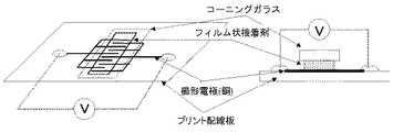
上記製法によって得たフィルム状接着剤を用いて、厚み0.7mmのコーニングガラス(#7059、コーニング社製)と、プリント基板上にライン幅100μm、ピッチ200μm、厚み35μmの銅回路を櫛型状に形成した櫛型電極とを、熱圧着装置(加熱方式:コンスタントヒート型、東レエンジニアリング株式会社製)を用いて150℃、2MPaで20秒間の加熱加圧を行って幅2mmにわたり接続し、時間経過後圧力開放して、接続体を作製した(図1参照)。この時、あらかじめ櫛型電極上に、フィルム状回路接続材料の接着面を貼り付けた後、70℃、0.5MPaで5秒間加熱加圧して仮接続し、その後、フッ素樹脂フィルムを剥離してもう一方の被着体であるコーニングガラスと接続した。
【0021】
(比較例1)
DtBMPを含有していない他は実施例1と同様にフィルム状接着剤を調整し、櫛型電極とコーニングガラスを加熱圧着により接続体を作製した。
【0022】
実施例1、比較例1で作製した接続体について接続直後の初期抵抗及び85℃、85%RHの条件で100時間、100Vの電圧を印加しながら高温高湿状態に曝した後の絶縁抵抗を評価した。絶縁抵抗の評価は、前記接続体に100Vの電圧を60秒間印加した後の抵抗値を絶縁抵抗計(株式会社アドバンテスト製R8340)で測定し、隣接回路間の抵抗50点の平均とした。また、金属顕微鏡を用いて、接続直後と耐湿試験後の外観を観察した。その結果を表1に示した。
【0023】
【表1】
実施例1で得た接続体については、耐湿試験後も初期の絶縁抵抗を持続しており、かつ外観の変化も無く、良好な接着剤であることを示した。
これに対して、DtBMPを添加していない比較例1の場合、耐湿試験後の絶縁抵抗は初期の絶縁抵抗を維持できずに低い値となり、かつ電極の腐食が観察され、信頼性が低いことが分かる。
【0025】
(実施例2)
実施例1のフィルム状接着剤を用いて、金バンプ(高さ:30μm、バンプ数:184)付きチップと、Ni/Auめっき銅回路プリント基板(電極高さ:20μm、基板厚み0.8mm)との接続を以下に示すように行った。
フィルム状接着剤の片面を銅回路プリント基板に60℃、0.5MPaの条件で20秒間加熱圧着して、仮接続させた。次に、チップのバンプと銅回路プリント基板との位置合わせを行い、フィルム状接着剤のもう一方の面のフッ素樹脂フィルムを剥離して、150℃、50g/バンプ、20秒の条件でチップ上方から加熱圧着して半導体装置を作製した。
上記半導体装置を85℃、85%RHの条件で500時間放置した後の接続抵抗を測定したところ、1バンプあたり最高で10mΩ、平均で2mΩであり、良好な接続抵抗を示した。
また、チップ及び銅回路プリント基板を剥離して外観を観察したところ、回路基板上の電極及びチップ上のバンプの腐食等は認められず、良好であった。
【0026】
【発明の効果】
本発明によれば、接着剤中に酸が存在しても回路電極の腐食が無く、しかも低温短時間で接着可能となり、接続信頼性に優れる。また、貯蔵安定性に優れる接着剤組成物、回路接続材料、回路接続用接着剤組成物を提供することができる。
【図面の簡単な説明】
【図1】 実施例1の試験方法を説明するための模式図。[0001]
BACKGROUND OF THE INVENTION
The present invention relates to an adhesive composition, a circuit connection material, an adhesive composition for circuit connection, a connection body, and a semiconductor device.
[0002]
[Prior art]
In the semiconductor element and the liquid crystal display element, various adhesives are conventionally used for the purpose of bonding various members in the element. The adhesives are required to have various properties such as adhesiveness, heat resistance, reliability in a high temperature and high humidity state. In addition, adherends used for bonding include organic substrates such as printed wiring boards and polyimides, circuit electrode surfaces made of metals such as copper and aluminum, and inorganic materials such as ITO, and silicon wafers. A variety of substrates are used, and molecular design is required for each adherend.
Conventionally, as an adhesive for the semiconductor element and the liquid crystal display element, a thermosetting resin using an epoxy resin having high adhesiveness and high reliability has been used. As a constituent component of the resin, a curing agent such as an epoxy resin, a phenol resin having reactivity with the epoxy resin, and a thermal latent catalyst for promoting the reaction between the epoxy resin and the curing agent are generally used. The heat latent catalyst is an important factor for determining the curing temperature and the curing rate, and various compounds have been used from the viewpoint of storage stability at room temperature and curing rate during heating. The curing conditions in the actual process were that desired adhesion was obtained by curing at a temperature of 170 to 250 ° C. for 1 to 3 hours.
In addition, as a method for connecting circuit electrodes using an adhesive, two circuit boards are bonded to each other, and as an adhesive for obtaining electrical conduction between these electrodes, a thermoplastic material such as styrene or polyester, Thermosetting materials such as epoxy and silicone are used. In this case, conductive particles are blended in the adhesive, and electrical connection is obtained in the thickness direction of the adhesive by pressurization (for example, JP-A-55-104007), and connection without using conductive particles is performed. In some cases, electrical connection is obtained by contact of fine irregularities on the electrode surface by pressurizing (for example, JP-A-60-262430).
However, with the recent high integration of semiconductor elements and high definition of liquid crystal elements, the pitch between elements and wirings has narrowed, and there has been a risk of adversely affecting peripheral members due to heating during curing. In order to further reduce the cost, it is necessary to improve the throughput, and adhesion at low temperature (100 to 170 ° C.), short time (within 1 hour, preferably tens of seconds or less), in other words, low temperature rapid curing. Is required. In order to achieve this low-temperature rapid curing, it is necessary to use a thermal latent catalyst having a low activation energy. In this case, it is very difficult to combine storage stability near room temperature.
JP-A-11-60899 and JP-A-11-116778 disclose a method using photocationic polymerization of an epoxy resin as an adhesive having both storage stability and low-temperature curability. These are composed of an epoxy resin and a photoacid generator that generates a strong acid by light irradiation, and is a method of curing by light irradiation at room temperature.
[0003]
[Problems to be solved by the invention]
However, in the case of the photocationic polymerization, since a strong acid such as Bronsted acid or Lewis acid is used as a polymerization catalyst, corrosion of a circuit electrode composed of a metal substrate or a metal and an inorganic material as an adherend is promoted, There has been a problem that the reliability of the connection body is significantly lowered. In addition, when an epoxy resin is used for the adhesive, impurity ions remaining in the epoxy resin cause corrosion of circuit electrodes formed of a metal such as copper or aluminum on the adherend or an inorganic material such as ITO. The function as a connection body will be reduced.
[0004]
The present invention relates to an adhesive composition, a circuit connecting material, and an adhesive for circuit connection, which prevent deterioration of the reliability of an element due to corrosion of an adherend composed of a metal and an inorganic material, and is excellent in storage stability at room temperature. A composition, a connection body, and a semiconductor device are provided.
[0005]
[Means for Solving the Problems]
The present invention relates to [1] (a) light irradiation at 150 to 750 nm, heating at 80 to 200 ° C., or a combination of light irradiation and heating, a curable adhesive, (b) general formula (A) And / or a compound represented by the general formula (B), and (a) a curable adhesive is cured with an epoxy resin and a resin having at least one phenolic hydroxyl group, thiol group, or carboxyl group in the molecule. An accelerator, or a cationic polymerizable resin and a polymerization initiator that generates cations by heat and / or light irradiation, and (a) 100 parts by weight of the curable adhesive ( b) An adhesive composition containing 0.5 to 30 parts by weight of the compound represented by formula (A) and / or formula (B) .
[Chemical 3]
[Formula 4]
Further, the present invention is an adhesive in the composition, the adhesive composition further comprising a conductive particle according to [2] above SL [1]. Moreover, this invention is a circuit connection material which made the shape of the adhesive composition as described in [ 3 ] said [1] or [2] into a film form. The present invention also provides [ 4 ] an adhesive which is interposed between circuit members having circuit electrodes facing each other and presses the circuit members having circuit electrodes facing each other to electrically connect the electrodes in the pressing direction. It is a composition, The adhesive composition is an adhesive composition for circuit connection which is the adhesive composition or circuit connection material according to any one of [1] to [ 3 ]. Moreover, this invention is a connection body which connected the circuit member using the adhesive composition for circuit connection as described in [ 5 ] said [ 4 ]. The present invention also provides [ 6 ] the adhesive composition or circuit connection material according to any one of [1] to [ 3 ] above between the electrode of the semiconductor element and the circuit electrode of the semiconductor mounting substrate, This is a semiconductor device in which pressure is applied to electrically connect electrodes in the pressing direction.
[0006]
DETAILED DESCRIPTION OF THE INVENTION
The (a) curable adhesive used in the present invention is not particularly limited as long as it is cured by light irradiation at 150 to 750 nm, heating at 80 to 200 ° C., and further using light irradiation and heating in combination. Can be used.
Examples of such curable adhesives include resins having one or more radical polymerizable groups such as acryloyl group, methacryloyl group, allyl group, maleimide group, and vinyl group in the molecule, and radicals by heat and / or light irradiation. And a radical polymerization system comprising a generated polymerization initiator.
In addition, epoxy resins, resins having at least one phenolic hydroxyl group, thiol group, and carboxyl group in the molecule, curing accelerators, and cationic polymerizable resins such as epoxy resins and vinyl ether resins, and cation by heat and / or light irradiation An epoxy curing system comprising a polymerization initiator that generates
[0007]
As the compound represented by (b) general formula (A) and / or general formula (B) used in the present invention, the following compounds (C) to (J) are particularly preferable.
[Chemical formula 5]
(B) The amount of the compound represented by the general formula (A) and / or the general formula (B) may be added to (a) 100 parts by weight of the curable adhesive (b) the general formula (A) and / or The amount of the compound represented by the general formula (B) is 0.5 to 30 parts by weight, preferably 1 to 10 parts by weight. If the amount added exceeds this range, the curability may be adversely affected.
[0009]
Examples of the conductive particles used in the present invention include metal particles such as Au, Ag, Ni, Cu, and solder, and carbon. Further, non-conductive glass, ceramic, plastic, or the like may be used as a core, and the core, metal particles, or carbon may be coated on the core. In the case of conductive particles with plastic as the core and the core coated with the metal, metal particles or carbon, or hot-melt metal particles, the contact area with the electrode during connection increases because it is deformable by heating and pressing. This is preferable because the reliability is improved. In addition, fine particles with the surface of these conductive particles coated with a polymer resin or the like suppress short-circuiting due to contact between particles when the amount of conductive particles is increased, and improve insulation between electrode circuits. Therefore, it may be used alone or mixed with conductive particles as appropriate.
[0010]
The average particle diameter of the conductive particles is preferably 1 to 18 μm from the viewpoint of dispersibility and conductivity. The amount of the conductive particles used is not particularly limited, but is preferably 0.1 to 30% by volume, and preferably 0.1 to 10% by volume with respect to 100% of the total amount of the adhesive composition. More preferred. If this value is less than 0.1% by volume, the conductivity tends to be inferior, and if it exceeds 30% by volume, a short circuit tends to occur. The volume% is determined based on the volume of each component before curing at 23 ° C., but the volume of each component can be converted from weight to volume using specific gravity. In addition, do not dissolve or swell the component in a graduated cylinder, etc., but put in a suitable solvent (water, alcohol, etc.) that wets the component well. You can ask for it.
[0011]
In the adhesive composition of the present invention, an additive such as an adhesion improver such as a coupling agent and a leveling agent may be added as appropriate.
[0012]
In the adhesive composition of the present invention, various polymers may be appropriately added for the purpose of thickening or forming a film. The polymer to be used is not particularly limited, but it may not adversely affect (a) the curable adhesive, (b) the compound represented by the general formula (A) and / or the general formula (B) and the conductive particles. It is essential. Such polymers include general purpose phenoxy resins such as polyimide, polyamide, bisphenol A type phenoxy resin, bisphenol F type phenoxy resin, bisphenol A / bisphenol F copolymer type phenoxy resin, polymethacrylates, polyacrylates and polyimides. Polyurethanes, polyesters, polyvinyl butyral, SBS and its epoxy modified products, SEBS and its modified products, and the like can be used. These can be used alone or in admixture of two or more. Furthermore, these polymers may contain siloxane bonds and fluorine substituents. These can be suitably used as the adhesive composition as long as the resins to be mixed are completely compatible with each other or microphase separation occurs and the mixture becomes cloudy. The larger the molecular weight of the polymer, the easier it is to form a film, and the melt viscosity that affects the fluidity as an adhesive can be set in a wide range. The molecular weight is not particularly limited, but a general weight average molecular weight is preferably from 5,000 to 150,000, particularly preferably from 10,000 to 80,000. If this value is less than 5,000, the film formability tends to be inferior, and if it exceeds 150,000, the compatibility with other components tends to deteriorate. The amount used is preferably 20 to 320 parts by weight with respect to 100 parts by weight of the radical polymerization system or epoxy curing system. When the amount used is less than 20 parts by weight or more than 320 parts by weight, fluidity and adhesiveness tend to decrease.
[0013]
The adhesive composition of the present invention can be used in the form of a paste when it is liquid at room temperature. In the case of a solid at room temperature, it may be heated and used, or may be made into a paste using a solvent. The solvent that can be used is not particularly limited as long as it is not reactive with the adhesive composition and additives, and exhibits sufficient solubility, but has a boiling point of 50 to 150 ° C. at normal pressure. Those are preferred. When the boiling point is 50 ° C. or lower, there is a risk of volatilization if left at room temperature, which restricts use in an open system. Moreover, when the boiling point is 150 ° C. or higher, it is difficult to volatilize the solvent, which may adversely affect the reliability after bonding.
[0014]
The adhesive composition of the present invention can also be used as a circuit connection material in the form of a film. A solution prepared by adding a solvent or the like to the adhesive composition as necessary is applied to a peelable substrate such as a fluororesin film, a polyethylene terephthalate film, or a release paper, or a substrate such as a nonwoven fabric is impregnated with the solution. Can be used as a film after removing the solvent and the like. Use in the form of a film is more convenient from the viewpoint of handleability.
[0015]
The adhesive composition of the present invention can be adhered by light irradiation, heating, or simultaneous use of heat and pressure simultaneously with light irradiation. By using these in combination, adhesion at a lower temperature and in a shorter time becomes possible. The light irradiation is preferably in the wavelength range of 150 to 750 nm, and is cured at a dose of 0.1 to 10 J / cm 2 using a low pressure mercury lamp, a medium pressure mercury lamp, a high pressure mercury lamp, a xenon lamp, or a metal halide lamp. Can do. The heating temperature is not particularly limited as long as it is below the decomposition point of the adhesive composition, but a temperature of 80 to 200 ° C. is preferable. The pressure is not particularly limited as long as it does not damage the adherend, but is generally preferably 0.1 to 10 MPa. These heating and pressurization are preferably performed in the range of 0.5 seconds to 3 hours.
[0016]
The adhesive composition of the present invention can be used as an adhesive for different types of adherends having different thermal expansion coefficients. Specifically, it is used as a semiconductor element adhesive material typified by anisotropic conductive adhesive, silver paste, silver film, etc., circuit connection material, CSP elastomer, CSP underfill material, LOC tape, etc. Can do.
[0017]
Below, an example of the connection of the electrode using the circuit connection material which used the adhesive composition for circuit connections of this invention and the adhesive composition as a film is demonstrated.
A circuit connection material in the form of a film made of an adhesive composition is present between electrodes on the substrate, irradiated with light of 150 to 750 nm, and then heated and pressed to adhere both electrodes and bond between the substrates. Can be connected to the electrode. As the substrate for forming the electrodes, semiconductors, inorganic substances such as glass and ceramics, organic substances such as polyimide and polycarbonate, and combinations of these composites such as glass / epoxy can be applied.
When the adhesive composition for circuit connection according to the present invention is used, it is possible to connect materials having different coefficients of thermal expansion, which has been difficult in the past, and to prevent deterioration of element reliability due to corrosion of the adherend. Can be applied to a wide range of material connections.
[0018]
In the present invention, as circuit members, chip parts such as semiconductor chips, resistor chips, capacitor chips, substrates such as printed boards, flexible wiring boards based on polyimide and polyester, indium oxide-tin oxide on glass such as liquid crystal panels A transparent electrode or the like wired with (ITO), chromium, aluminum or the like is used.
Since the adhesive composition of the present invention and the adhesive composition for circuit connection can be connected at a relatively low temperature, the thermal stress during connection is small, and the reliability after connecting a fine circuit can be drastically improved. Therefore, the efficiency of circuit connection work is improved and the yield is also improved. Further, since the corrosion of the electrode can be prevented, the reliability after the connection of the fine circuit can be dramatically improved.
[0019]
【Example】
Hereinafter, the present invention will be specifically described based on examples, but the present invention is not limited thereto.
[0020]
Example 1
40 g of phenoxy resin (PKHC, trade name of Union Carbide, average molecular weight 45,000) was dissolved in 60 g of methyl ethyl ketone to obtain a solution having a solid content of 40% by weight. As the epoxy resin, bisphenol A type liquid epoxy resin (Epicoat 828, product name manufactured by Yuka Shell Epoxy Co., Ltd., epoxy equivalent 184) is used, and aromatic sulfonium salt (Sun Aid SI-100L, Sanshin Chemical Co., Ltd.) as a latent catalyst. Company name, 2,6-di-tert-butyl-4-methylpyridine (DtBMP, manufactured by Aldrich) was used as the compound represented by the general formula (A) and / or the general formula (B). Further, a nickel layer having a thickness of 0.2 μm is provided on the surface of particles having polystyrene as a core, and a gold layer having a thickness of 0.02 μm is provided on the outside of the nickel layer. Particles were made.
It is blended so that it becomes phenoxy resin 50, epoxy resin 50, latent catalyst 3, DtBMP 2 in solid weight ratio, and 1.5% by volume of conductive particles are further dispersed and coated on a fluororesin film having a thickness of 80 μm. And a film adhesive having an adhesive layer thickness of 40 μm was obtained by hot air drying at 70 ° C. for 10 minutes.
Using a film adhesive obtained by the above manufacturing method, a 0.7 mm thick Corning glass (# 7059, manufactured by Corning) and a copper circuit having a line width of 100 μm, a pitch of 200 μm, and a thickness of 35 μm on a printed board are comb-shaped. The comb-shaped electrodes formed in the above are connected over a width of 2 mm by applying heat and pressure at 150 ° C. and 2 MPa for 20 seconds using a thermocompression bonding apparatus (heating method: constant heat type, manufactured by Toray Engineering Co., Ltd.). After the passage of time, the pressure was released to produce a connection body (see FIG. 1). At this time, after adhering the adhesive surface of the film-like circuit connecting material on the comb-shaped electrode in advance, the film is temporarily connected by heating and pressing at 70 ° C. and 0.5 MPa for 5 seconds, and then the fluororesin film is peeled off. It connected with the coning glass which is another adherend.
[0021]
(Comparative Example 1)
A film adhesive was prepared in the same manner as in Example 1 except that it did not contain DtBMP, and a connected body was prepared by thermocompression bonding of a comb-shaped electrode and Corning glass.
[0022]
About the connection body produced in Example 1 and Comparative Example 1, the initial resistance immediately after connection and the insulation resistance after being exposed to a high temperature and high humidity state while applying a voltage of 100 V for 100 hours under the conditions of 85 ° C. and 85% RH evaluated. Insulation resistance was evaluated by measuring the resistance value after applying a voltage of 100 V to the connection body for 60 seconds with an insulation resistance meter (R8340 manufactured by Advantest Co., Ltd.), and taking the average of the resistance of 50 points between adjacent circuits. Further, the appearance immediately after the connection and after the moisture resistance test was observed using a metal microscope. The results are shown in Table 1.
[0023]
[Table 1]
About the connection body obtained in Example 1, the initial insulation resistance was maintained after the moisture resistance test, and the appearance was not changed, indicating that it was a good adhesive.
On the other hand, in the case of Comparative Example 1 in which DtBMP was not added, the insulation resistance after the moisture resistance test was low because the initial insulation resistance could not be maintained, and the corrosion of the electrode was observed and the reliability was low. I understand.
[0025]
(Example 2)
Using the film adhesive of Example 1, a chip with gold bumps (height: 30 μm, number of bumps: 184) and a Ni / Au plated copper circuit printed circuit board (electrode height: 20 μm, substrate thickness 0.8 mm) The connection was made as shown below.
One side of the film adhesive was temporarily bonded to a copper circuit printed circuit board by thermocompression bonding at 60 ° C. and 0.5 MPa for 20 seconds. Next, the bumps of the chip and the copper circuit printed board are aligned, the fluororesin film on the other side of the film adhesive is peeled off, and the upper part of the chip under the conditions of 150 ° C., 50 g / bump, 20 seconds. The semiconductor device was manufactured by thermocompression bonding.
When the connection resistance after the semiconductor device was allowed to stand for 500 hours under the conditions of 85 ° C. and 85% RH was measured, the maximum per bump was 10 mΩ, and the average was 2 mΩ, indicating good connection resistance.
Further, when the chip and the copper circuit printed board were peeled and the appearance was observed, the corrosion on the electrodes on the circuit board and the bumps on the chip was not recognized, and it was good.
[0026]
【The invention's effect】
According to the present invention, even if an acid is present in the adhesive, the circuit electrode is not corroded, and can be bonded at a low temperature in a short time, and the connection reliability is excellent. Moreover, the adhesive composition excellent in storage stability, a circuit connection material, and the adhesive composition for circuit connection can be provided.
[Brief description of the drawings]
FIG. 1 is a schematic diagram for explaining a test method of Example 1. FIG.
Claims (6)
前記(a)硬化性接着剤が、エポキシ樹脂と分子内にフェノール性水酸基、チオール基、カルボキシル基を少なくとも一つ以上有する樹脂と硬化促進剤とを含むもの、又は、カチオン重合性樹脂と熱および/又は光照射よってカチオンを発生する重合開始剤とを含むものであり、
前記(a)硬化性接着剤100重量部に対して、前記(b)一般式(A)および/または一般式(B)で示される化合物0.5〜30重量部含有する接着剤組成物。
The (a) curable adhesive comprises an epoxy resin and a resin having at least one phenolic hydroxyl group, thiol group, or carboxyl group in the molecule and a curing accelerator, or a cationic polymerizable resin and heat and And / or a polymerization initiator that generates cations by light irradiation,
An adhesive composition containing 0.5 to 30 parts by weight of the compound represented by the general formula (A) and / or the general formula (B) with respect to 100 parts by weight of the (a) curable adhesive .
Priority Applications (1)
| Application Number | Priority Date | Filing Date | Title |
|---|---|---|---|
| JP2000286292A JP4635312B2 (en) | 2000-09-21 | 2000-09-21 | Adhesive composition, circuit connection material, adhesive composition for circuit connection, connector and semiconductor device |
Applications Claiming Priority (1)
| Application Number | Priority Date | Filing Date | Title |
|---|---|---|---|
| JP2000286292A JP4635312B2 (en) | 2000-09-21 | 2000-09-21 | Adhesive composition, circuit connection material, adhesive composition for circuit connection, connector and semiconductor device |
Publications (2)
| Publication Number | Publication Date |
|---|---|
| JP2002097441A JP2002097441A (en) | 2002-04-02 |
| JP4635312B2 true JP4635312B2 (en) | 2011-02-23 |
Family
ID=18770233
Family Applications (1)
| Application Number | Title | Priority Date | Filing Date |
|---|---|---|---|
| JP2000286292A Expired - Fee Related JP4635312B2 (en) | 2000-09-21 | 2000-09-21 | Adhesive composition, circuit connection material, adhesive composition for circuit connection, connector and semiconductor device |
Country Status (1)
| Country | Link |
|---|---|
| JP (1) | JP4635312B2 (en) |
Families Citing this family (4)
| Publication number | Priority date | Publication date | Assignee | Title |
|---|---|---|---|---|
| US7239013B2 (en) | 2002-07-18 | 2007-07-03 | Hitachi Chemical Co., Ltd. | Multilayer wiring board, method for producing the same, semiconductor device and radio electronic device |
| JP4248827B2 (en) * | 2002-07-18 | 2009-04-02 | 日立化成工業株式会社 | Multilayer wiring board and manufacturing method thereof |
| ATE441843T1 (en) * | 2004-01-27 | 2009-09-15 | Mettler Toledo Ag | FORCE MEASUREMENT CELL WITH STRAIN GAUGES WITH ADHESIVE LAYER MADE OF INORGANIC-ORGANIC HYBRID POLYMER (ORMOCER) |
| JP2005325312A (en) * | 2004-05-17 | 2005-11-24 | Hitachi Chem Co Ltd | Adhesive composition, film-like adhesive and circuit connecting material using the same, circuit member connecting structure, and manufacturing method thereof |
Family Cites Families (3)
| Publication number | Priority date | Publication date | Assignee | Title |
|---|---|---|---|---|
| US5968674A (en) * | 1997-10-14 | 1999-10-19 | Xerox Corporation | Conductive polymer coatings and processes thereof |
| JP4099878B2 (en) * | 1998-10-23 | 2008-06-11 | 日立化成工業株式会社 | Circuit member mounting method |
| JP5011599B2 (en) * | 2000-05-23 | 2012-08-29 | 日立化成工業株式会社 | Adhesive composition, adhesive composition for circuit connection, circuit connection material, connector and semiconductor device |
-
2000
- 2000-09-21 JP JP2000286292A patent/JP4635312B2/en not_active Expired - Fee Related
Also Published As
| Publication number | Publication date |
|---|---|
| JP2002097441A (en) | 2002-04-02 |
Similar Documents
| Publication | Publication Date | Title |
|---|---|---|
| JP4304508B2 (en) | Adhesive composition, adhesive composition for circuit connection, connector and semiconductor device | |
| CN102533136B (en) | Adhesive composition, and connection structure for circuit member | |
| JP4760070B2 (en) | Adhesive, adhesive for circuit connection, connector and semiconductor device | |
| JP5251393B2 (en) | Adhesive composition, adhesive for circuit connection, and connection body using the same | |
| WO2008065997A1 (en) | Adhesive and connection structure using the same | |
| KR20210134875A (en) | Adhesive composition and connected structure | |
| JP2014122353A (en) | Adhesive composition, circuit connecting adhesive, and connection body | |
| JP2002097443A (en) | Adhesive composition, circuit connecting material and connecting body using the same | |
| JP2011037953A (en) | Adhesive agent composition, circuit-connecting structure and semiconductor device | |
| JP2009074066A (en) | Adhesive composition, film adhesive, circuit connecting adhesive, connector, and semiconductor device | |
| JP2006199778A (en) | Adhesive composition, adhesive for use in circuit connection, method for connecting circuits using the same, and connected body | |
| JP3858740B2 (en) | Adhesive composition for circuit connection and circuit connection structure using the same | |
| JP2009256581A (en) | Adhesive composition, adhesive for circuit connection and connected product using the same | |
| JP4635312B2 (en) | Adhesive composition, circuit connection material, adhesive composition for circuit connection, connector and semiconductor device | |
| JP5111711B2 (en) | Adhesive composition, adhesive composition for circuit connection, and circuit connection method | |
| JP4635313B2 (en) | Adhesive composition, adhesive composition for circuit connection, circuit connection material, connector and semiconductor device | |
| JP4513147B2 (en) | Circuit connection method | |
| JP4649815B2 (en) | Adhesive composition for circuit connection and circuit connection structure using the same | |
| JP4635287B2 (en) | Anisotropic conductive film | |
| JP2002167569A (en) | Adhesive composition, adhesive composition for connecting circuit, connected unit and semiconductor device | |
| JP2012046757A (en) | Adhesive for connecting circuit, and circuit connection method and connection body using the same | |
| WO2007046189A1 (en) | Adhesive composition, circuit connecting material, connection structure of circuit connenctor, and semiconductor devices | |
| JP2012046756A (en) | Adhesive for connecting circuit, and circuit connection method and connection body using the same | |
| JP5392333B2 (en) | Circuit connection adhesive, circuit connection method using the same, and connection body | |
| JP4797224B2 (en) | Adhesive composition, adhesive composition for circuit connection, connector and semiconductor device |
Legal Events
| Date | Code | Title | Description |
|---|---|---|---|
| A621 | Written request for application examination |
Free format text: JAPANESE INTERMEDIATE CODE: A621 Effective date: 20070815 |
|
| RD03 | Notification of appointment of power of attorney |
Free format text: JAPANESE INTERMEDIATE CODE: A7423 Effective date: 20071213 |
|
| A977 | Report on retrieval |
Free format text: JAPANESE INTERMEDIATE CODE: A971007 Effective date: 20100902 |
|
| A131 | Notification of reasons for refusal |
Free format text: JAPANESE INTERMEDIATE CODE: A131 Effective date: 20100921 |
|
| A521 | Request for written amendment filed |
Free format text: JAPANESE INTERMEDIATE CODE: A523 Effective date: 20101007 |
|
| TRDD | Decision of grant or rejection written | ||
| A01 | Written decision to grant a patent or to grant a registration (utility model) |
Free format text: JAPANESE INTERMEDIATE CODE: A01 Effective date: 20101026 |
|
| A01 | Written decision to grant a patent or to grant a registration (utility model) |
Free format text: JAPANESE INTERMEDIATE CODE: A01 |
|
| A61 | First payment of annual fees (during grant procedure) |
Free format text: JAPANESE INTERMEDIATE CODE: A61 Effective date: 20101108 |
|
| FPAY | Renewal fee payment (event date is renewal date of database) |
Free format text: PAYMENT UNTIL: 20131203 Year of fee payment: 3 |
|
| FPAY | Renewal fee payment (event date is renewal date of database) |
Free format text: PAYMENT UNTIL: 20131203 Year of fee payment: 3 |
|
| S531 | Written request for registration of change of domicile |
Free format text: JAPANESE INTERMEDIATE CODE: R313531 |
|
| S533 | Written request for registration of change of name |
Free format text: JAPANESE INTERMEDIATE CODE: R313533 |
|
| FPAY | Renewal fee payment (event date is renewal date of database) |
Free format text: PAYMENT UNTIL: 20131203 Year of fee payment: 3 |
|
| R350 | Written notification of registration of transfer |
Free format text: JAPANESE INTERMEDIATE CODE: R350 |
|
| LAPS | Cancellation because of no payment of annual fees |