JP4635113B2 - Manufacturing method of solid electrolytic capacitor - Google Patents
Manufacturing method of solid electrolytic capacitor Download PDFInfo
- Publication number
- JP4635113B2 JP4635113B2 JP2010525123A JP2010525123A JP4635113B2 JP 4635113 B2 JP4635113 B2 JP 4635113B2 JP 2010525123 A JP2010525123 A JP 2010525123A JP 2010525123 A JP2010525123 A JP 2010525123A JP 4635113 B2 JP4635113 B2 JP 4635113B2
- Authority
- JP
- Japan
- Prior art keywords
- solid electrolytic
- electrolytic capacitor
- layer
- dispersant
- capacitor element
- Prior art date
- Legal status (The legal status is an assumption and is not a legal conclusion. Google has not performed a legal analysis and makes no representation as to the accuracy of the status listed.)
- Expired - Fee Related
Links
- 239000003990 capacitor Substances 0.000 title claims description 127
- 239000007787 solid Substances 0.000 title claims description 122
- 238000004519 manufacturing process Methods 0.000 title claims description 48
- 239000002270 dispersing agent Substances 0.000 claims description 51
- 239000011347 resin Substances 0.000 claims description 40
- 229920005989 resin Polymers 0.000 claims description 40
- 239000004020 conductor Substances 0.000 claims description 35
- 239000002904 solvent Substances 0.000 claims description 33
- 239000004065 semiconductor Substances 0.000 claims description 25
- LFQSCWFLJHTTHZ-UHFFFAOYSA-N Ethanol Chemical compound CCO LFQSCWFLJHTTHZ-UHFFFAOYSA-N 0.000 claims description 24
- 238000007654 immersion Methods 0.000 claims description 22
- 238000000034 method Methods 0.000 claims description 22
- BQCADISMDOOEFD-UHFFFAOYSA-N Silver Chemical compound [Ag] BQCADISMDOOEFD-UHFFFAOYSA-N 0.000 claims description 18
- OKTJSMMVPCPJKN-UHFFFAOYSA-N Carbon Chemical compound [C] OKTJSMMVPCPJKN-UHFFFAOYSA-N 0.000 claims description 14
- 229910052709 silver Inorganic materials 0.000 claims description 14
- 239000004332 silver Substances 0.000 claims description 14
- 239000011230 binding agent Substances 0.000 claims description 12
- 239000000843 powder Substances 0.000 claims description 11
- 229910052799 carbon Inorganic materials 0.000 claims description 10
- -1 fatty acid compound Chemical class 0.000 claims description 8
- 235000014113 dietary fatty acids Nutrition 0.000 claims description 4
- 239000000194 fatty acid Substances 0.000 claims description 4
- 229930195729 fatty acid Natural products 0.000 claims description 4
- 239000000113 methacrylic resin Substances 0.000 claims description 4
- 239000011248 coating agent Substances 0.000 claims description 3
- 238000000576 coating method Methods 0.000 claims description 3
- 235000019441 ethanol Nutrition 0.000 description 13
- 229920001940 conductive polymer Polymers 0.000 description 9
- 239000000126 substance Substances 0.000 description 9
- 238000006243 chemical reaction Methods 0.000 description 8
- YXFVVABEGXRONW-UHFFFAOYSA-N Toluene Chemical compound CC1=CC=CC=C1 YXFVVABEGXRONW-UHFFFAOYSA-N 0.000 description 6
- 238000001721 transfer moulding Methods 0.000 description 6
- WRIDQFICGBMAFQ-UHFFFAOYSA-N (E)-8-Octadecenoic acid Natural products CCCCCCCCCC=CCCCCCCC(O)=O WRIDQFICGBMAFQ-UHFFFAOYSA-N 0.000 description 5
- LQJBNNIYVWPHFW-UHFFFAOYSA-N 20:1omega9c fatty acid Natural products CCCCCCCCCCC=CCCCCCCCC(O)=O LQJBNNIYVWPHFW-UHFFFAOYSA-N 0.000 description 5
- QSBYPNXLFMSGKH-UHFFFAOYSA-N 9-Heptadecensaeure Natural products CCCCCCCC=CCCCCCCCC(O)=O QSBYPNXLFMSGKH-UHFFFAOYSA-N 0.000 description 5
- CSCPPACGZOOCGX-UHFFFAOYSA-N Acetone Chemical compound CC(C)=O CSCPPACGZOOCGX-UHFFFAOYSA-N 0.000 description 5
- ZQPPMHVWECSIRJ-UHFFFAOYSA-N Oleic acid Natural products CCCCCCCCC=CCCCCCCCC(O)=O ZQPPMHVWECSIRJ-UHFFFAOYSA-N 0.000 description 5
- 239000005642 Oleic acid Substances 0.000 description 5
- 239000002019 doping agent Substances 0.000 description 5
- QXJSBBXBKPUZAA-UHFFFAOYSA-N isooleic acid Natural products CCCCCCCC=CCCCCCCCCC(O)=O QXJSBBXBKPUZAA-UHFFFAOYSA-N 0.000 description 5
- 229910052751 metal Inorganic materials 0.000 description 5
- 239000002184 metal Substances 0.000 description 5
- ZQPPMHVWECSIRJ-KTKRTIGZSA-N oleic acid Chemical compound CCCCCCCC\C=C/CCCCCCCC(O)=O ZQPPMHVWECSIRJ-KTKRTIGZSA-N 0.000 description 5
- 239000000243 solution Substances 0.000 description 5
- 235000021355 Stearic acid Nutrition 0.000 description 4
- 230000015572 biosynthetic process Effects 0.000 description 4
- 239000011888 foil Substances 0.000 description 4
- WABPQHHGFIMREM-UHFFFAOYSA-N lead(0) Chemical compound [Pb] WABPQHHGFIMREM-UHFFFAOYSA-N 0.000 description 4
- 239000000178 monomer Substances 0.000 description 4
- QIQXTHQIDYTFRH-UHFFFAOYSA-N octadecanoic acid Chemical compound CCCCCCCCCCCCCCCCCC(O)=O QIQXTHQIDYTFRH-UHFFFAOYSA-N 0.000 description 4
- OQCDKBAXFALNLD-UHFFFAOYSA-N octadecanoic acid Natural products CCCCCCCC(C)CCCCCCCCC(O)=O OQCDKBAXFALNLD-UHFFFAOYSA-N 0.000 description 4
- 239000008117 stearic acid Substances 0.000 description 4
- ZWEHNKRNPOVVGH-UHFFFAOYSA-N 2-Butanone Chemical compound CCC(C)=O ZWEHNKRNPOVVGH-UHFFFAOYSA-N 0.000 description 3
- WEVYAHXRMPXWCK-UHFFFAOYSA-N Acetonitrile Chemical compound CC#N WEVYAHXRMPXWCK-UHFFFAOYSA-N 0.000 description 3
- UHOVQNZJYSORNB-UHFFFAOYSA-N Benzene Chemical compound C1=CC=CC=C1 UHOVQNZJYSORNB-UHFFFAOYSA-N 0.000 description 3
- YMWUJEATGCHHMB-UHFFFAOYSA-N Dichloromethane Chemical compound ClCCl YMWUJEATGCHHMB-UHFFFAOYSA-N 0.000 description 3
- RTZKZFJDLAIYFH-UHFFFAOYSA-N Diethyl ether Chemical compound CCOCC RTZKZFJDLAIYFH-UHFFFAOYSA-N 0.000 description 3
- OKKJLVBELUTLKV-UHFFFAOYSA-N Methanol Chemical compound OC OKKJLVBELUTLKV-UHFFFAOYSA-N 0.000 description 3
- ZMXDDKWLCZADIW-UHFFFAOYSA-N N,N-Dimethylformamide Chemical compound CN(C)C=O ZMXDDKWLCZADIW-UHFFFAOYSA-N 0.000 description 3
- ROSDCCJGGBNDNL-UHFFFAOYSA-N [Ta].[Pb] Chemical compound [Ta].[Pb] ROSDCCJGGBNDNL-UHFFFAOYSA-N 0.000 description 3
- 238000009835 boiling Methods 0.000 description 3
- 239000002134 carbon nanofiber Substances 0.000 description 3
- 239000002608 ionic liquid Substances 0.000 description 3
- VLKZOEOYAKHREP-UHFFFAOYSA-N n-Hexane Chemical compound CCCCCC VLKZOEOYAKHREP-UHFFFAOYSA-N 0.000 description 3
- PXHVJJICTQNCMI-UHFFFAOYSA-N nickel Substances [Ni] PXHVJJICTQNCMI-UHFFFAOYSA-N 0.000 description 3
- 229920000123 polythiophene Polymers 0.000 description 3
- 238000004804 winding Methods 0.000 description 3
- JAJIPIAHCFBEPI-UHFFFAOYSA-N 9,10-dioxoanthracene-1-sulfonic acid Chemical compound O=C1C2=CC=CC=C2C(=O)C2=C1C=CC=C2S(=O)(=O)O JAJIPIAHCFBEPI-UHFFFAOYSA-N 0.000 description 2
- HEDRZPFGACZZDS-UHFFFAOYSA-N Chloroform Chemical compound ClC(Cl)Cl HEDRZPFGACZZDS-UHFFFAOYSA-N 0.000 description 2
- IAZDPXIOMUYVGZ-UHFFFAOYSA-N Dimethylsulphoxide Chemical compound CS(C)=O IAZDPXIOMUYVGZ-UHFFFAOYSA-N 0.000 description 2
- YNQLUTRBYVCPMQ-UHFFFAOYSA-N Ethylbenzene Chemical compound CCC1=CC=CC=C1 YNQLUTRBYVCPMQ-UHFFFAOYSA-N 0.000 description 2
- LRHPLDYGYMQRHN-UHFFFAOYSA-N N-Butanol Chemical compound CCCCO LRHPLDYGYMQRHN-UHFFFAOYSA-N 0.000 description 2
- IMNFDUFMRHMDMM-UHFFFAOYSA-N N-Heptane Chemical compound CCCCCCC IMNFDUFMRHMDMM-UHFFFAOYSA-N 0.000 description 2
- CTQNGGLPUBDAKN-UHFFFAOYSA-N O-Xylene Chemical compound CC1=CC=CC=C1C CTQNGGLPUBDAKN-UHFFFAOYSA-N 0.000 description 2
- OFBQJSOFQDEBGM-UHFFFAOYSA-N Pentane Chemical compound CCCCC OFBQJSOFQDEBGM-UHFFFAOYSA-N 0.000 description 2
- NBIIXXVUZAFLBC-UHFFFAOYSA-N Phosphoric acid Chemical compound OP(O)(O)=O NBIIXXVUZAFLBC-UHFFFAOYSA-N 0.000 description 2
- WYURNTSHIVDZCO-UHFFFAOYSA-N Tetrahydrofuran Chemical compound C1CCOC1 WYURNTSHIVDZCO-UHFFFAOYSA-N 0.000 description 2
- 230000009471 action Effects 0.000 description 2
- 230000032683 aging Effects 0.000 description 2
- 229910045601 alloy Inorganic materials 0.000 description 2
- 239000000956 alloy Substances 0.000 description 2
- 229910052782 aluminium Inorganic materials 0.000 description 2
- 239000013256 coordination polymer Substances 0.000 description 2
- JHIVVAPYMSGYDF-UHFFFAOYSA-N cyclohexanone Chemical compound O=C1CCCCC1 JHIVVAPYMSGYDF-UHFFFAOYSA-N 0.000 description 2
- 239000006185 dispersion Substances 0.000 description 2
- 239000003822 epoxy resin Substances 0.000 description 2
- 229910002804 graphite Inorganic materials 0.000 description 2
- 239000010439 graphite Substances 0.000 description 2
- IPCSVZSSVZVIGE-UHFFFAOYSA-N hexadecanoic acid Chemical compound CCCCCCCCCCCCCCCC(O)=O IPCSVZSSVZVIGE-UHFFFAOYSA-N 0.000 description 2
- 239000003273 ketjen black Substances 0.000 description 2
- VNWKTOKETHGBQD-UHFFFAOYSA-N methane Chemical compound C VNWKTOKETHGBQD-UHFFFAOYSA-N 0.000 description 2
- 229910052759 nickel Inorganic materials 0.000 description 2
- 239000003960 organic solvent Substances 0.000 description 2
- 230000001590 oxidative effect Effects 0.000 description 2
- 238000007747 plating Methods 0.000 description 2
- 229920003229 poly(methyl methacrylate) Polymers 0.000 description 2
- 229920000647 polyepoxide Polymers 0.000 description 2
- 229920000642 polymer Polymers 0.000 description 2
- 238000006116 polymerization reaction Methods 0.000 description 2
- 230000008569 process Effects 0.000 description 2
- 230000008439 repair process Effects 0.000 description 2
- 239000007784 solid electrolyte Substances 0.000 description 2
- 229910052715 tantalum Inorganic materials 0.000 description 2
- GUVRBAGPIYLISA-UHFFFAOYSA-N tantalum atom Chemical compound [Ta] GUVRBAGPIYLISA-UHFFFAOYSA-N 0.000 description 2
- VZGDMQKNWNREIO-UHFFFAOYSA-N tetrachloromethane Chemical compound ClC(Cl)(Cl)Cl VZGDMQKNWNREIO-UHFFFAOYSA-N 0.000 description 2
- 239000010936 titanium Substances 0.000 description 2
- 229910052719 titanium Inorganic materials 0.000 description 2
- 238000003466 welding Methods 0.000 description 2
- 239000008096 xylene Substances 0.000 description 2
- RYHBNJHYFVUHQT-UHFFFAOYSA-N 1,4-Dioxane Chemical compound C1COCCO1 RYHBNJHYFVUHQT-UHFFFAOYSA-N 0.000 description 1
- VBICKXHEKHSIBG-UHFFFAOYSA-N 1-monostearoylglycerol Chemical compound CCCCCCCCCCCCCCCCCC(=O)OCC(O)CO VBICKXHEKHSIBG-UHFFFAOYSA-N 0.000 description 1
- YMMGRPLNZPTZBS-UHFFFAOYSA-N 2,3-dihydrothieno[2,3-b][1,4]dioxine Chemical compound O1CCOC2=C1C=CS2 YMMGRPLNZPTZBS-UHFFFAOYSA-N 0.000 description 1
- OAYXUHPQHDHDDZ-UHFFFAOYSA-N 2-(2-butoxyethoxy)ethanol Chemical compound CCCCOCCOCCO OAYXUHPQHDHDDZ-UHFFFAOYSA-N 0.000 description 1
- 239000004925 Acrylic resin Substances 0.000 description 1
- 229920000178 Acrylic resin Polymers 0.000 description 1
- RYGMFSIKBFXOCR-UHFFFAOYSA-N Copper Chemical compound [Cu] RYGMFSIKBFXOCR-UHFFFAOYSA-N 0.000 description 1
- 229910000881 Cu alloy Inorganic materials 0.000 description 1
- 239000001856 Ethyl cellulose Substances 0.000 description 1
- ZZSNKZQZMQGXPY-UHFFFAOYSA-N Ethyl cellulose Chemical compound CCOCC1OC(OC)C(OCC)C(OCC)C1OC1C(O)C(O)C(OC)C(CO)O1 ZZSNKZQZMQGXPY-UHFFFAOYSA-N 0.000 description 1
- DCXXMTOCNZCJGO-UHFFFAOYSA-N Glycerol trioctadecanoate Natural products CCCCCCCCCCCCCCCCCC(=O)OCC(OC(=O)CCCCCCCCCCCCCCCCC)COC(=O)CCCCCCCCCCCCCCCCC DCXXMTOCNZCJGO-UHFFFAOYSA-N 0.000 description 1
- FXHOOIRPVKKKFG-UHFFFAOYSA-N N,N-Dimethylacetamide Chemical compound CN(C)C(C)=O FXHOOIRPVKKKFG-UHFFFAOYSA-N 0.000 description 1
- SECXISVLQFMRJM-UHFFFAOYSA-N N-Methylpyrrolidone Chemical compound CN1CCCC1=O SECXISVLQFMRJM-UHFFFAOYSA-N 0.000 description 1
- 235000021314 Palmitic acid Nutrition 0.000 description 1
- 229920000265 Polyparaphenylene Polymers 0.000 description 1
- ATJFFYVFTNAWJD-UHFFFAOYSA-N Tin Chemical compound [Sn] ATJFFYVFTNAWJD-UHFFFAOYSA-N 0.000 description 1
- RTAQQCXQSZGOHL-UHFFFAOYSA-N Titanium Chemical compound [Ti] RTAQQCXQSZGOHL-UHFFFAOYSA-N 0.000 description 1
- 150000001242 acetic acid derivatives Chemical class 0.000 description 1
- 239000006230 acetylene black Substances 0.000 description 1
- 239000002253 acid Substances 0.000 description 1
- 150000001298 alcohols Chemical class 0.000 description 1
- 150000001338 aliphatic hydrocarbons Chemical class 0.000 description 1
- HSFWRNGVRCDJHI-UHFFFAOYSA-N alpha-acetylene Natural products C#C HSFWRNGVRCDJHI-UHFFFAOYSA-N 0.000 description 1
- WUOACPNHFRMFPN-UHFFFAOYSA-N alpha-terpineol Chemical compound CC1=CCC(C(C)(C)O)CC1 WUOACPNHFRMFPN-UHFFFAOYSA-N 0.000 description 1
- XAGFODPZIPBFFR-UHFFFAOYSA-N aluminium Chemical compound [Al] XAGFODPZIPBFFR-UHFFFAOYSA-N 0.000 description 1
- 229910000147 aluminium phosphate Inorganic materials 0.000 description 1
- 150000001408 amides Chemical class 0.000 description 1
- 239000007864 aqueous solution Substances 0.000 description 1
- 229910021393 carbon nanotube Inorganic materials 0.000 description 1
- 239000002041 carbon nanotube Substances 0.000 description 1
- 230000015556 catabolic process Effects 0.000 description 1
- 230000008859 change Effects 0.000 description 1
- 239000003795 chemical substances by application Substances 0.000 description 1
- 229910052804 chromium Inorganic materials 0.000 description 1
- 239000013065 commercial product Substances 0.000 description 1
- 230000000052 comparative effect Effects 0.000 description 1
- 239000000470 constituent Substances 0.000 description 1
- 229910052802 copper Inorganic materials 0.000 description 1
- 239000010949 copper Substances 0.000 description 1
- 230000003247 decreasing effect Effects 0.000 description 1
- 238000006731 degradation reaction Methods 0.000 description 1
- SQIFACVGCPWBQZ-UHFFFAOYSA-N delta-terpineol Natural products CC(C)(O)C1CCC(=C)CC1 SQIFACVGCPWBQZ-UHFFFAOYSA-N 0.000 description 1
- 238000013461 design Methods 0.000 description 1
- 230000006866 deterioration Effects 0.000 description 1
- 238000007598 dipping method Methods 0.000 description 1
- 238000001035 drying Methods 0.000 description 1
- 150000002170 ethers Chemical class 0.000 description 1
- 229920001249 ethyl cellulose Polymers 0.000 description 1
- 235000019325 ethyl cellulose Nutrition 0.000 description 1
- 238000001704 evaporation Methods 0.000 description 1
- 230000008020 evaporation Effects 0.000 description 1
- 238000000605 extraction Methods 0.000 description 1
- 230000009477 glass transition Effects 0.000 description 1
- 229910052737 gold Inorganic materials 0.000 description 1
- 150000008282 halocarbons Chemical class 0.000 description 1
- 229930195733 hydrocarbon Natural products 0.000 description 1
- 238000001746 injection moulding Methods 0.000 description 1
- 239000003350 kerosene Substances 0.000 description 1
- 150000002576 ketones Chemical class 0.000 description 1
- 229910052749 magnesium Inorganic materials 0.000 description 1
- 238000005259 measurement Methods 0.000 description 1
- 230000005012 migration Effects 0.000 description 1
- 238000013508 migration Methods 0.000 description 1
- 239000000203 mixture Substances 0.000 description 1
- 229910052750 molybdenum Inorganic materials 0.000 description 1
- 238000000465 moulding Methods 0.000 description 1
- WQEPLUUGTLDZJY-UHFFFAOYSA-N n-Pentadecanoic acid Natural products CCCCCCCCCCCCCCC(O)=O WQEPLUUGTLDZJY-UHFFFAOYSA-N 0.000 description 1
- 229910052758 niobium Inorganic materials 0.000 description 1
- 239000010955 niobium Substances 0.000 description 1
- GUCVJGMIXFAOAE-UHFFFAOYSA-N niobium atom Chemical compound [Nb] GUCVJGMIXFAOAE-UHFFFAOYSA-N 0.000 description 1
- 150000002825 nitriles Chemical class 0.000 description 1
- 235000021313 oleic acid Nutrition 0.000 description 1
- 239000007800 oxidant agent Substances 0.000 description 1
- 229910052763 palladium Inorganic materials 0.000 description 1
- KDLHZDBZIXYQEI-UHFFFAOYSA-N palladium Substances [Pd] KDLHZDBZIXYQEI-UHFFFAOYSA-N 0.000 description 1
- 229920000553 poly(phenylenevinylene) Polymers 0.000 description 1
- 229920001197 polyacetylene Polymers 0.000 description 1
- 229920000767 polyaniline Polymers 0.000 description 1
- 229920001721 polyimide Polymers 0.000 description 1
- 239000009719 polyimide resin Substances 0.000 description 1
- 230000000379 polymerizing effect Effects 0.000 description 1
- 229920000128 polypyrrole Polymers 0.000 description 1
- 229920001296 polysiloxane Polymers 0.000 description 1
- 239000011148 porous material Substances 0.000 description 1
- FVSKHRXBFJPNKK-UHFFFAOYSA-N propionitrile Chemical compound CCC#N FVSKHRXBFJPNKK-UHFFFAOYSA-N 0.000 description 1
- 238000010992 reflux Methods 0.000 description 1
- 229910052707 ruthenium Inorganic materials 0.000 description 1
- 229920002545 silicone oil Polymers 0.000 description 1
- 229920002050 silicone resin Polymers 0.000 description 1
- 238000005245 sintering Methods 0.000 description 1
- 230000035882 stress Effects 0.000 description 1
- 150000003462 sulfoxides Chemical class 0.000 description 1
- 229940116411 terpineol Drugs 0.000 description 1
- YLQBMQCUIZJEEH-UHFFFAOYSA-N tetrahydrofuran Natural products C=1C=COC=1 YLQBMQCUIZJEEH-UHFFFAOYSA-N 0.000 description 1
- 229920001187 thermosetting polymer Polymers 0.000 description 1
- 238000012546 transfer Methods 0.000 description 1
- 229910052721 tungsten Inorganic materials 0.000 description 1
- 229910052720 vanadium Inorganic materials 0.000 description 1
- 238000005406 washing Methods 0.000 description 1
- 239000003232 water-soluble binding agent Substances 0.000 description 1
Images
Classifications
-
- H—ELECTRICITY
- H01—ELECTRIC ELEMENTS
- H01G—CAPACITORS; CAPACITORS, RECTIFIERS, DETECTORS, SWITCHING DEVICES, LIGHT-SENSITIVE OR TEMPERATURE-SENSITIVE DEVICES OF THE ELECTROLYTIC TYPE
- H01G9/00—Electrolytic capacitors, rectifiers, detectors, switching devices, light-sensitive or temperature-sensitive devices; Processes of their manufacture
- H01G9/004—Details
- H01G9/04—Electrodes or formation of dielectric layers thereon
- H01G9/042—Electrodes or formation of dielectric layers thereon characterised by the material
- H01G9/0425—Electrodes or formation of dielectric layers thereon characterised by the material specially adapted for cathode
-
- H—ELECTRICITY
- H01—ELECTRIC ELEMENTS
- H01G—CAPACITORS; CAPACITORS, RECTIFIERS, DETECTORS, SWITCHING DEVICES, LIGHT-SENSITIVE OR TEMPERATURE-SENSITIVE DEVICES OF THE ELECTROLYTIC TYPE
- H01G9/00—Electrolytic capacitors, rectifiers, detectors, switching devices, light-sensitive or temperature-sensitive devices; Processes of their manufacture
- H01G9/004—Details
- H01G9/008—Terminals
- H01G9/012—Terminals specially adapted for solid capacitors
-
- H—ELECTRICITY
- H01—ELECTRIC ELEMENTS
- H01G—CAPACITORS; CAPACITORS, RECTIFIERS, DETECTORS, SWITCHING DEVICES, LIGHT-SENSITIVE OR TEMPERATURE-SENSITIVE DEVICES OF THE ELECTROLYTIC TYPE
- H01G9/00—Electrolytic capacitors, rectifiers, detectors, switching devices, light-sensitive or temperature-sensitive devices; Processes of their manufacture
- H01G9/15—Solid electrolytic capacitors
Landscapes
- Engineering & Computer Science (AREA)
- Power Engineering (AREA)
- Microelectronics & Electronic Packaging (AREA)
- Chemical & Material Sciences (AREA)
- Materials Engineering (AREA)
- Fixed Capacitors And Capacitor Manufacturing Machines (AREA)
Description
本発明は、固体電解コンデンサ素子を高温の溶融樹脂によって外装しても、固体電解コンデンサ素子の等価直列抵抗(以下、ESRと表記することがある。)をほとんど上昇させないで固体電解コンデンサを製造する方法に関する。 The present invention produces a solid electrolytic capacitor with little increase in the equivalent series resistance (hereinafter sometimes referred to as ESR) of the solid electrolytic capacitor element even if the solid electrolytic capacitor element is packaged with a high-temperature molten resin. Regarding the method.
樹脂外装された固体電解コンデンサは、1または2以上の固体電解コンデンサ素子をリードフレームに配置し、それを樹脂溶液に浸漬する方法、溶融樹脂によってトランスファー成形する方法などによって製造される。
樹脂溶液に浸漬する方法は、外装樹脂の厚さが薄いのでピンホールを生じやすく、また寸法精度が低い。一方、トランスファー成形法は、浸漬法に比べ、品質が均一で寸法精度が高く、肉厚、複雑な形状の成形が可能で、硬化時間が短く、さらにバリが少なく後仕上げが容易である。そのため、固体電解コンデンサの大量製造ではトランスファー成形法が多く採用されている。The resin-covered solid electrolytic capacitor is manufactured by placing one or more solid electrolytic capacitor elements on a lead frame and immersing them in a resin solution, or transfer molding with a molten resin.
In the method of immersing in a resin solution, pinholes are easily generated because the thickness of the exterior resin is thin, and the dimensional accuracy is low. On the other hand, the transfer molding method has a uniform quality and high dimensional accuracy, can be molded into a thick and complex shape, has a short curing time, and has few burrs and is easy to finish. Therefore, the transfer molding method is often used in mass production of solid electrolytic capacitors.
しかし、トランスファー成形法は、溶融樹脂から固体電解コンデンサ素子に加わる圧力および熱量が高い。そのために、トランスファー成形法による樹脂外装において、固体電解コンデンサ素子の劣化が進み、ESRが上昇してしまうことがある。近年使用されている固体電解コンデンサはESRが小さい値を示すものであるので、わずかなESRの上昇であっても、電子機器の設計においては見逃すことができない問題である。 However, in the transfer molding method, the pressure and heat applied from the molten resin to the solid electrolytic capacitor element are high. Therefore, in the resin exterior by the transfer molding method, the deterioration of the solid electrolytic capacitor element may progress and the ESR may increase. Since solid electrolytic capacitors used in recent years have low ESR values, even a slight increase in ESR is a problem that cannot be overlooked in the design of electronic equipment.
ESRのレベルを低下させる方法として、例えば、特許文献1には、弁作用金属粉末と固形水溶性バインダーと有機溶剤可溶性バインダーとを有機溶剤中で混合して造粒した後、該造粒物に陽極リードを植立して、成形体を形成する工程と、該成形体内のバインダーを溶剤によって洗浄除去する工程と、高温・真空中で焼結する工程とを有することを特徴とする固体電解コンデンサ陽極体の製造方法が開示されている。この陽極体を用いることによって、tanδ、ESRのレベルおよびバラツキが小さく、漏れ電流特性を改善した固体電解コンデンサが得られると特許文献1には記載されている。
As a method for reducing the level of ESR, for example,
特許文献2には、陽極電極箔と陰極電極箔とをセパレータを介して巻き取ることにより巻回素子を作製し、該巻回素子を、セパレータの構成成分のうちの少なくとも1種を溶解しうる溶剤に浸漬し、セパレータを減量し、次いで該巻回素子内に固体電解質層を形成する固体電解コンデンサの製法が開示されている。
In
特許文献3には、表面に酸化皮膜を有する陽極箔と、陰極箔との間にセパレータを介在させて巻回したコンデンサ素子を、酸化剤溶液と重合性モノマー溶液とに順次浸漬して、該重合性モノマーを化学重合させることにより、導電性高分子層を前記コンデンサ素子内に形成する工程を有する、固体電解コンデンサの製造方法であって、前記重合性モノマー溶液の溶媒がイオン液体であり、前記導電性高分子形成工程の後、前記コンデンサ素子を、前記イオン液体を溶解しうる溶媒に浸漬してコンデンサ素子中の前記イオン液体を溶解除去することを特徴とする、固体電解コンデンサの製造方法が開示されている。この製造方法によって、高い静電容量出現率で、容量が大きく且つ漏れ電流の少ない固体電解コンデンサが製造できると特許文献3は述べている。
In
特許文献4には、陽極体、誘電体層、カーボングラファイト層および銀ペースト層を形成された固体電解コンデンサ素子に、シリコーン樹脂またはシリコーン油層を設け、次いで該素子をアセトンやトルエンなどの有機溶媒に浸漬し、または振動を加えて表面のシリコーン層を除去し、次いで外装樹脂層を設ける、固体電解コンデンサの製造方法が開示されている。この製造方法によって、固体電解コンデンサの耐湿性が向上し、それによって、静電容量変化率および誘電正接の劣化を小さくできると、特許文献4は述べている。
In
しかしながら、これら特許文献に記載の製造方法では、該固体電解コンデンサ素子を樹脂外装(樹脂封止)する時に加わる熱によって、固体電解コンデンサ素子のESRが上昇してしまい、設計値どおりの低いESRの固体電解コンデンサを得るのは難しかった。
本発明の目的は、固体電解コンデンサ素子を高温の溶融樹脂によって外装しても、固体電解コンデンサ素子のESRをほとんど上昇させないで、固体電解コンデンサを製造する方法を提供することである。However, in the manufacturing methods described in these patent documents, the ESR of the solid electrolytic capacitor element increases due to heat applied when the solid electrolytic capacitor element is resin-sealed (resin-sealed), and the ESR of the low ESR as designed It was difficult to obtain a solid electrolytic capacitor.
An object of the present invention is to provide a method of manufacturing a solid electrolytic capacitor with almost no increase in ESR of the solid electrolytic capacitor element even if the solid electrolytic capacitor element is packaged with a high-temperature molten resin.
本発明者は、上記の目的を達成するために鋭意検討した結果、分散剤を含む導電性ペーストを用いて導電体層を形成させた後、または分散剤を含む導電性ペーストを用いて陰極端子に固体電解コンデンサ素子の導電体層を電気的に接続させた後に、該固体電解コンデンサ素子を溶剤に浸漬すると、その後に高温の溶融樹脂による外装を行っても、固体電解コンデンサ素子のESRをほとんど上昇させないで固体電解コンデンサを製造できることを見出した。本発明は、この知見に基づいてさらに詳細に検討して、完成するに至ったものである。 As a result of intensive studies to achieve the above object, the present inventor has formed a conductor layer using a conductive paste containing a dispersant, or a cathode terminal using a conductive paste containing a dispersant. After electrically connecting the conductive layer of the solid electrolytic capacitor element to the solid electrolytic capacitor element, the solid electrolytic capacitor element is immersed in a solvent. It has been found that a solid electrolytic capacitor can be produced without raising it. The present invention has been studied in more detail based on this finding, and has been completed.
すなわち、本発明は以下のものである。
〈1〉 陽極体表面に誘電体層を形成し、該誘電体層の上に半導体層を形成し、次いで該半導体層の上に分散剤を含む導電性ペーストを用いて導電体層を形成することによって、固体電解コンデンサ素子を得、
該固体電解コンデンサ素子を溶剤に浸漬し、
前記浸漬の前または後に前記導電体層を陰極端子に電気的に接続し、
次いで、樹脂外装することを含む、固体電解コンデンサの製造方法。
〈2〉 陽極体表面に誘電体層を形成し、該誘電体層の上に半導体層を形成し、次いで該半導体層の上に導電体層を形成することによって、固体電解コンデンサ素子を得、
前記導電体層を陰極端子に分散剤を含む導電性ペーストを用いて電気的に接続し、
陰極端子に接続された固体電解コンデンサ素子を溶剤に浸漬し、
次いで、樹脂外装することを含む、固体電解コンデンサの製造方法。
〈3〉 浸漬に用いる溶剤が、導電性ペーストに含まれる結合剤を溶解または膨潤させないものである、〈1〉または〈2〉に記載の固体電解コンデンサの製造方法。That is, the present invention is as follows.
<1> A dielectric layer is formed on the surface of the anode body, a semiconductor layer is formed on the dielectric layer, and then a conductor layer is formed on the semiconductor layer using a conductive paste containing a dispersant. By obtaining a solid electrolytic capacitor element,
Immerse the solid electrolytic capacitor element in a solvent,
Electrically connecting the conductor layer to the cathode terminal before or after the immersion,
Then, the manufacturing method of a solid electrolytic capacitor including covering with resin.
<2> A solid electrolytic capacitor element is obtained by forming a dielectric layer on the surface of the anode body, forming a semiconductor layer on the dielectric layer, and then forming a conductor layer on the semiconductor layer,
The conductor layer is electrically connected to the cathode terminal using a conductive paste containing a dispersant,
Immerse the solid electrolytic capacitor element connected to the cathode terminal in a solvent,
Then, the manufacturing method of a solid electrolytic capacitor including covering with resin.
<3> The method for producing a solid electrolytic capacitor according to <1> or <2>, wherein the solvent used for the immersion does not dissolve or swell the binder contained in the conductive paste.
〈4〉 浸漬に用いる溶剤が、アルコールである、〈1〉または〈2〉に記載の固体電解コンデンサの製造方法。
〈5〉 陽極体表面に誘電体層を形成し、該誘電体層の上に半導体層を形成し、次いで該半導体層の上に導電性ペーストを用いて導電体層を形成することによって固体電解コンデンサ素子を得、前記導電体層を陰極端子に導電性ペーストを用いて電気的に接続し、次いで、樹脂外装することを含む工程において、
分散剤を含む導電性ペーストを用いて導電体層を形成させた若しくは分散剤を含む導電性ペーストを用いて陰極端子に固体電解コンデンサ素子の導電体層を電気的に接続させた後で、且つ樹脂外装の前に、導電体層中に残存する分散剤の量を700質量ppm未満にすることをさらに含む、固体電解コンデンサの製造方法。
〈6〉 導電体層が、導電性カーボンペーストを用いて得た層と分散剤を含む銀ペーストを用いて得た層とを含む、〈1〉〜〈5〉のいずれか一項に記載の固体電解コンデンサの製造方法。
〈7〉 導電性ペーストが、導電性粉とビヒクルとを含むものである、〈1〉〜〈6〉のいずれか一項に記載の固体電解コンデンサの製造方法。
〈8〉 ビヒクルが、結合剤を含むものである、〈7〉に記載の固体電解コンデンサの製造方法。
〈9〉 前記結合剤が、メタクリル樹脂である、〈8〉に記載の固体電解コンデンサの製造方法。
〈10〉 前記分散剤が、高級脂肪酸化合物を含むものである、〈1〉〜〈9〉のいずれか一項に記載の固体電解コンデンサの製造方法。
〈11〉 前記〈1)〜〈10〉のいずれか一項に記載の製造方法で得られる固体電解コンデンサ。<4> The method for producing a solid electrolytic capacitor according to <1> or <2>, wherein the solvent used for the immersion is alcohol.
<5> A solid electrolyte is formed by forming a dielectric layer on the surface of the anode body, forming a semiconductor layer on the dielectric layer, and then forming a conductor layer on the semiconductor layer using a conductive paste. In a process including obtaining a capacitor element, electrically connecting the conductor layer to the cathode terminal using a conductive paste, and then covering the resin,
After forming a conductor layer using a conductive paste containing a dispersant or electrically connecting a conductor layer of a solid electrolytic capacitor element to a cathode terminal using a conductive paste containing a dispersant, and The method for producing a solid electrolytic capacitor, further comprising setting the amount of the dispersant remaining in the conductor layer to less than 700 ppm by mass before the resin sheathing.
<6> The conductor layer according to any one of <1> to <5>, wherein the conductor layer includes a layer obtained using a conductive carbon paste and a layer obtained using a silver paste containing a dispersant. A method for producing a solid electrolytic capacitor.
<7> The method for producing a solid electrolytic capacitor according to any one of <1> to <6>, wherein the conductive paste includes conductive powder and a vehicle.
<8> The method for producing a solid electrolytic capacitor according to <7>, wherein the vehicle includes a binder.
<9> The method for producing a solid electrolytic capacitor according to <8>, wherein the binder is a methacrylic resin.
<10> The method for producing a solid electrolytic capacitor according to any one of <1> to <9>, wherein the dispersant includes a higher fatty acid compound.
<11> A solid electrolytic capacitor obtained by the production method according to any one of <1) to <10>.
本発明の固体電解コンデンサの製造方法によれば、固体電解コンデンサ素子を高温の溶融樹脂によって外装しても、固体電解コンデンサ素子のESRをほとんど上昇させずに固体電解コンデンサを製造することができる。その結果、ESRが小さい樹脂外装された固体電解コンデンサを設計どおりに製造することができる。 According to the method for manufacturing a solid electrolytic capacitor of the present invention, even when the solid electrolytic capacitor element is packaged with a high-temperature molten resin, the solid electrolytic capacitor can be manufactured with almost no increase in ESR of the solid electrolytic capacitor element. As a result, a resin-coated solid electrolytic capacitor with a low ESR can be manufactured as designed.
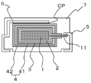
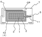
本発明の製造方法を、実施形態に係る固体電解コンデンサを示す図面を参照しながら説明する。なお、本発明の製造方法で得られる固体電解コンデンサは下記の実施形態に示したものに限定されるものではなく、その要旨を変更しない範囲において適宜変更して実施できるものである。図1および図2は本発明の製造方法によって得られる実施形態の固体電解コンデンサの断面説明図である。該固体電解コンデンサは、固体電解コンデンサ素子と陽極端子と陰極端子とが外装樹脂で封止されているものである。 A manufacturing method of the present invention will be described with reference to the drawings showing a solid electrolytic capacitor according to an embodiment. In addition, the solid electrolytic capacitor obtained by the manufacturing method of the present invention is not limited to the one shown in the following embodiment, and can be appropriately modified and implemented within a range not changing the gist thereof. 1 and 2 are cross-sectional explanatory views of a solid electrolytic capacitor of an embodiment obtained by the manufacturing method of the present invention. In the solid electrolytic capacitor, a solid electrolytic capacitor element, an anode terminal, and a cathode terminal are sealed with an exterior resin.
本発明の固体電解コンデンサの製造方法では、先ず、固体電解コンデンサ素子を製造する。
固体電解コンデンサ素子は、陽極体1の表面に誘電体層2を形成し、該誘電体層2の上に半導体層3を形成し、次いで該半導体層3の上に導電体層を形成することによって得られる。In the method for producing a solid electrolytic capacitor of the present invention, first, a solid electrolytic capacitor element is produced.
In the solid electrolytic capacitor element, the
本発明に用いられる陽極体は、タンタル、アルミニウム、ニオブ、チタン等の弁作用金属又はこのような弁作用金属を主成分とする合金で作製されたものが好ましい。陽極体は前記弁作用金属粉または合金粉の焼結体であることが特に好ましい。該焼結体は多孔質体であることが好ましい。また、図1および図2に示した陽極体1はリード線11が陽極体から延出されている。
The anode body used in the present invention is preferably made of a valve metal such as tantalum, aluminum, niobium, titanium, or an alloy containing such a valve metal as a main component. The anode body is particularly preferably a sintered body of the valve action metal powder or alloy powder. The sintered body is preferably a porous body. Further, in the
本発明の製造方法では、先ず、陽極体表面に誘電体層を形成する。誘電体層の形成には、化成処理が行われる。この化成処理によって陽極体の表面に酸化物が生成する。この酸化物層が誘電体層になる。化成処理には、一般的に行われている電解化成方法を用いることができる。 In the production method of the present invention, first, a dielectric layer is formed on the surface of the anode body. A chemical conversion treatment is performed to form the dielectric layer. By this chemical conversion treatment, an oxide is generated on the surface of the anode body. This oxide layer becomes a dielectric layer. For the chemical conversion treatment, a generally performed electrolytic chemical conversion method can be used.
該誘電体層の上に半導体層3を形成する。半導体層は導電性ポリマーを含有するものが好ましい。
導電性ポリマーとしては、ポリチオフェン系誘導体、ポリフェニレンビニレン系誘導体、ポリピロール系誘導体、ポリアニリン系誘導体、ポリアセチレン系誘導体、ポリフェニレン系誘導体、ポリイソチアナフテン誘導体等が挙げられる。本発明では、導電性ポリマーが共役二重結合を有する高分子を含む場合に好適であり、特にポリチオフェン骨格を有するポリマーを含む場合に好適である。上記導電性ポリマーは、1種単独でもしくは2種以上を組み合わせて用いることができる。導電性ポリマーにはドーパントが通常含まれている。該ドーパントは、固体電解コンデンサ用の導電性ポリマーにおいて一般的に用いられているドーパントから選択できる。ドーパントとしては、良好な特性を持つ固体電解コンデンサを得ることができる観点からスルホン酸化合物が好ましい。導電性ポリマーの形成には、電解重合法、化学酸化重合法のいずれを用いてもよい。なお、半導体層の形成途中または形成後に修復化成(再化成)を行ってもよい。修復化成には、一般的に行われている電解化成方法を用いることができる。A
Examples of the conductive polymer include polythiophene derivatives, polyphenylene vinylene derivatives, polypyrrole derivatives, polyaniline derivatives, polyacetylene derivatives, polyphenylene derivatives, polyisothianaphthene derivatives, and the like. In the present invention, the conductive polymer is suitable when it contains a polymer having a conjugated double bond, and is particularly suitable when it contains a polymer having a polythiophene skeleton. The said conductive polymer can be used individually by 1 type or in combination of 2 or more types. The conductive polymer usually contains a dopant. The dopant can be selected from dopants commonly used in conductive polymers for solid electrolytic capacitors. As the dopant, a sulfonic acid compound is preferable from the viewpoint of obtaining a solid electrolytic capacitor having good characteristics. Either the electropolymerization method or the chemical oxidative polymerization method may be used to form the conductive polymer. In addition, you may perform repair chemical conversion (re-chemical conversion) in the middle of formation of a semiconductor layer, or after formation. For the repair conversion, a generally performed electrolytic formation method can be used.
図1および図2では、陽極体1の外表面にのみ誘電体層2および半導体層3が形成されているように描かれているが、陽極体が多孔質体である場合には、誘電体層および半導体層は多孔質体内部の細孔の表面にも形成される。
1 and 2, the
次に、上記の半導体層3の表面を覆うようにして導電体層4を形成する。導電体層の形成には、通常、導電性ペーストが用いられる。図1では、半導体層3の上に導電性カーボンペーストを用いてカーボン層41を設け、さらにこのカーボン層41の上に、銀ペーストを用いて銀層42を設けている。また、図2では、上記のカーボン層41を設けずに、半導体層3の表面を覆うようにして、銀ペーストを用いて銀層42だけを設けている。
Next, the
導電性ペーストは導電性粉とビヒクルを主成分として含むものである。導電性粉としては、黒鉛、アセチレンブラック、ケッチェンブラック(ケッチェン・ブラック・インターナショナル社製導電性カーボンブラック)、カーボンナノチューブ、カーボンナノファイバー、気相法炭素繊維(VGCF)などの導電性カーボン;銀粉、銅粉などの金属粉が挙げられる。これら導電性粉には、分散性を保つために分散剤が添加されていることが多い。これら導電性ペーストのうち銀ペーストが好ましく用いられる。銀ペーストの主成分である銀粉には、Ag元素以外に、Au、Cu、Al、Ti、Pd、Ni、V、Ta、W、Mo、Cr、Ru、Mgなどの元素が含まれていても良い。これら元素が含まれているとエレクトロマイグレーション、ストレスマイグレーションに対する耐性に優れた固体電解コンデンサになることがある。 The conductive paste contains conductive powder and a vehicle as main components. Conductive carbon such as graphite, acetylene black, ketjen black (conductive carbon black manufactured by Ketjen Black International), carbon nanotube, carbon nanofiber, vapor grown carbon fiber (VGCF), etc .; silver powder And metal powders such as copper powder. In many cases, a dispersant is added to these conductive powders in order to maintain dispersibility. Of these conductive pastes, silver paste is preferably used. The silver powder as the main component of the silver paste may contain elements such as Au, Cu, Al, Ti, Pd, Ni, V, Ta, W, Mo, Cr, Ru, and Mg in addition to the Ag element. good. When these elements are contained, a solid electrolytic capacitor having excellent resistance to electromigration and stress migration may be obtained.
導電性ペーストのもう一方の主成分であるビヒクルは、結合剤と必要に応じて溶剤とを混合したものであることが好ましい。
結合剤としては、メタクリル樹脂、アクリル樹脂、エチルセルロースなどが挙げられる。また、結合剤として、熱硬化性の樹脂や、感光性樹脂を用いてもよい。これらのうち、本発明では、メタクリル樹脂が好ましく用いられる。
溶剤としては、テルピネオール、キシレン、ケロシン、ブチルカルビトール、酢酸エステル類などが挙げられる。導電性ペーストを所定箇所に塗布した後、該溶剤を除去することによって導電性ペーストが固化する。The vehicle, which is the other main component of the conductive paste, is preferably a mixture of a binder and, if necessary, a solvent.
Examples of the binder include methacrylic resin, acrylic resin, and ethyl cellulose. Further, as the binder, a thermosetting resin or a photosensitive resin may be used. Of these, methacrylic resin is preferably used in the present invention.
Examples of the solvent include terpineol, xylene, kerosene, butyl carbitol, and acetates. After applying the conductive paste to a predetermined location, the conductive paste is solidified by removing the solvent.
導電性ペーストに使用される導電性粉はナノオーダーからミクロンオーダーの大きさのものなので、ペースト内で導電性粉が凝集しないように分散剤が加えられている。分散剤としては、例えば、パルミチン酸、ステアリン酸、オレイン酸のような高級脂肪酸化合物が用いられる。 Since the conductive powder used for the conductive paste has a size of nano-order to micron order, a dispersant is added so that the conductive powder does not aggregate in the paste. As the dispersant, for example, higher fatty acid compounds such as palmitic acid, stearic acid, and oleic acid are used.
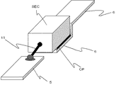
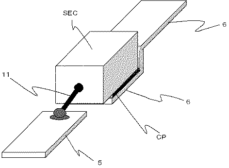
上記のようにして得た固体電解コンデンサ素子は、通常、陽極体1から延出させたリード線11に陽極端子5を電気的に接続させると共に、上記の導電体層4に陰極端子6を電気的に接続させる(図3参照)。陰極端子および陽極端子の取り付けには通常のリードフレームを用いることができる。
リード線と陽極端子との電気的接続には、通常、溶接や導電性ペーストによる接着などが用いられる。また、導電体層と陰極端子との電気的接続には、通常、銀ペーストなどの導電性ペーストによる接着が用いられる。なお、この電気的接続に用いられる導電性ペーストとしても上記に説明したものが挙げられる。In the solid electrolytic capacitor element obtained as described above, the
For electrical connection between the lead wire and the anode terminal, welding or adhesion with a conductive paste is usually used. Further, for electrical connection between the conductor layer and the cathode terminal, adhesion by a conductive paste such as a silver paste is usually used. In addition, what was demonstrated above is mentioned as an electrically conductive paste used for this electrical connection.
本発明の製造方法では、分散剤を含む導電性ペーストを用いて導電体層を形成させた若しくは分散剤を含む導電性ペーストを用いて陰極端子に固体電解コンデンサ素子の導電体層を電気的に接続させた後で、且つ樹脂外装の前に、導電体層中に残存する分散剤を700質量ppm未満、好ましくは20質量ppm以下にする。なお、残存分散剤の割合は、分散剤を含んでいる(含んでいた)導電体層に対する割合である。
残存分散剤の割合の調整法は特に限定されないが、本発明の製造方法の一態様では、分散剤を含む導電性ペーストを用いて導電体層を形成させた若しくは分散剤を含む導電性ペーストを用いて陰極端子に固体電解コンデンサ素子の導電体層を電気的に接続させた後で、且つ樹脂外装の前に、該固体電解コンデンサ素子または陰極端子に接続された固体電解コンデンサ素子を溶剤に浸漬する。この溶剤浸漬によって、残存分散剤の割合を調整することができる。In the production method of the present invention, a conductor layer is formed using a conductive paste containing a dispersant, or a conductive layer of a solid electrolytic capacitor element is electrically connected to a cathode terminal using a conductive paste containing a dispersant. After the connection and before the resin sheathing, the dispersant remaining in the conductor layer is made less than 700 ppm by mass, preferably 20 ppm by mass or less. In addition, the ratio of the residual dispersant is a ratio with respect to the conductor layer containing (containing) the dispersant.
The method for adjusting the ratio of the residual dispersant is not particularly limited, but in one embodiment of the production method of the present invention, the conductive paste containing the dispersant is formed using the conductive paste containing the dispersant or the conductive paste containing the dispersant is used. The solid electrolytic capacitor element or the solid electrolytic capacitor element connected to the cathode terminal is immersed in a solvent after electrically connecting the conductive layer of the solid electrolytic capacitor element to the cathode terminal and before the resin sheathing. To do. By this solvent immersion, the ratio of the residual dispersant can be adjusted.
浸漬に用いる溶剤は、分散剤を溶解可能なものであれば特に限定されず、例えば、ペンタン、ヘキサン、ヘプタン等の脂肪族炭化水素;ジクロロメタン、クロロホルム、四塩化炭素等のハロゲン化炭化水素;シクロヘキサン等の脂環式炭化水素;ベンゼン、トルエン、キシレン、エチルベンゼン等の芳香族炭化水素;メタノール、エタノール、ブタノール等のアルコール;アセトン、メチルエチルケトン、シクロヘキサノン等のケトン;アセトニトリル、プロピオンニトリル等のニトリル系溶媒;ジエチルエーテル、ジオキサン、テトラヒドロフラン等のエーテル;N,N−ジメチルホルムアミド、N,N−ジメチルアセタミド、N−メチルピロリドン等のアミド系溶媒;ジメチルスルホキシド等のスルホキシド類;等が挙げられる。浸漬に用いる溶剤は、導電性ペーストに含まれる結合剤を溶解または膨潤させないものが好ましく、特にアルコールが好ましい。 The solvent used for the immersion is not particularly limited as long as it can dissolve the dispersant. For example, aliphatic hydrocarbons such as pentane, hexane and heptane; halogenated hydrocarbons such as dichloromethane, chloroform and carbon tetrachloride; cyclohexane Alicyclic hydrocarbons such as benzene, toluene, xylene, ethylbenzene, etc .; alcohols such as methanol, ethanol, butanol; ketones such as acetone, methyl ethyl ketone, cyclohexanone; nitrile solvents such as acetonitrile, propiononitrile, etc .; And ethers such as diethyl ether, dioxane and tetrahydrofuran; amide solvents such as N, N-dimethylformamide, N, N-dimethylacetamide and N-methylpyrrolidone; sulfoxides such as dimethyl sulfoxide; The solvent used for the dipping is preferably one that does not dissolve or swell the binder contained in the conductive paste, and alcohol is particularly preferable.
浸漬時の溶剤温度は、特に制限されないが、好ましくは60〜160℃、より好ましくは70〜120℃である。常圧における沸点が低い溶剤を用いた場合に、該沸点以上の温度で該溶剤に浸漬するために加圧することができる。
浸漬時間は特に制限されないが、10分間〜10時間が好ましい。
この浸漬によって、導電性ペーストを用いて得られた導電体層4や導電性ペーストを用いて得られた陰極端子と導電体層との電気的接続層CPに残存する溶剤可溶分が除去される。溶剤可溶分の主なものとしては、導電性ペーストに含まれていた分散剤が挙げられる。この分散剤は、導電性ペースト内での導電性粉の分散を良くするために必要なものであるが、固体電解コンデンサ素子の導電体層や、陰極端子と導電体層との電気的接続層になってからは不必要になるものである。Although the solvent temperature at the time of immersion is not specifically limited, Preferably it is 60-160 degreeC, More preferably, it is 70-120 degreeC. When a solvent having a low boiling point at normal pressure is used, the solvent can be pressurized so as to be immersed in the solvent at a temperature equal to or higher than the boiling point.
The immersion time is not particularly limited, but is preferably 10 minutes to 10 hours.
By this immersion, the solvent soluble component remaining in the electrical connection layer CP between the
浸漬終了後、固体電解コンデンサ素子を溶剤から引き上げ、乾燥して溶剤を除去する。本発明の製造方法では、浸漬から乾燥までの操作を数回繰り返しても良い。また、導電性ペーストを用いて導電体層を形成させた後、および導電性ペーストを用いて陰極端子に固体電解コンデンサ素子の導電体層を電気的に接続させた後の、いずれか一方のときに、浸漬を行ってもよいし、両方のときに浸漬をそれぞれ行ってもよい。 After completion of the immersion, the solid electrolytic capacitor element is pulled up from the solvent and dried to remove the solvent. In the production method of the present invention, the operation from immersion to drying may be repeated several times. Also, either after the conductive layer is formed using the conductive paste and after the conductive layer of the solid electrolytic capacitor element is electrically connected to the cathode terminal using the conductive paste In addition, immersion may be performed, or immersion may be performed at both times.
次に、陽極端子5と陰極端子6とを外部に取り出すようにして樹脂外装を行う。樹脂外装の方法として、通常、射出成形法やトランスファー成形法が用いられる。外装樹脂には、エポキシ樹脂、ポリイミド樹脂などの公知の電気絶縁性樹脂が用いられる。
このようにして、樹脂外装された固体電解コンデンサが得られる。該固体電解コンデンサは、所望によりエージング処理を行うことができる。本発明の製造方法で得られる固体電解コンデンサは、各種電気回路または電子回路に装着し、使用することができる。Next, resin coating is performed so that the
In this manner, a resin-coated solid electrolytic capacitor is obtained. The solid electrolytic capacitor can be subjected to an aging treatment as desired. The solid electrolytic capacitor obtained by the production method of the present invention can be used by being mounted on various electric circuits or electronic circuits.
本発明の製造方法によって、固体電解コンデンサ素子を高温の溶融樹脂で外装しても、固体電解コンデンサ素子のESRをほとんど上昇させずに固体電解コンデンサを製造することができるようになる理由は、定かで無いが、次のように本発明者は推測する。
導電性ペーストに含まれている分散剤(高級脂肪酸化合物)は、高沸点物質であるために、ペーストを固化させる時の温度では除去されない。本発明の製造方法における固体電解コンデンサ素子を溶剤に浸漬するなどの残存分散剤の割合を調整する工程を経ない場合には、導電性ペーストに含まれていた分散剤が、ほぼそのまま、固体電解コンデンサ素子に残存することになる。樹脂外装では高温の溶融樹脂を金型に流し込むので、樹脂外装時に固体電解コンデンサ素子は高温状態に置かれる。また、金型から取り出した後に外装樹脂をガラス転移温度付近の高温にして硬化させるので、そのときにも固体電解コンデンサ素子は高温状態に数時間置かれる。このような固体電解コンデンサ素子が高温状態に置かれているときに、残存した分散剤が蒸発して導電体層の表面に浮き出たり、陰極端子の表面に付着したりして、半導体層と導電体層との界面や導電体層と陰極端子との界面における接触抵抗を高くし、ESRを押し上げていると考えられる。前述したように、固体電解コンデンサ素子を溶剤に浸漬する工程において導電性ペーストに含まれていた分散剤が除去される。そのために樹脂外装時にESRが上昇しなくなるのであろうと推測する。The reason why the manufacturing method of the present invention makes it possible to manufacture a solid electrolytic capacitor with almost no increase in the ESR of the solid electrolytic capacitor element even when the solid electrolytic capacitor element is packaged with a high-temperature molten resin. However, the present inventor estimates as follows.
Since the dispersant (higher fatty acid compound) contained in the conductive paste is a high boiling point substance, it is not removed at the temperature at which the paste is solidified. In the production method of the present invention, when the step of adjusting the ratio of the remaining dispersant, such as immersing the solid electrolytic capacitor element in a solvent, is not performed, the dispersant contained in the conductive paste is almost as it is. It will remain in the capacitor element. Since the high temperature molten resin is poured into the mold in the resin exterior, the solid electrolytic capacitor element is placed in a high temperature state during the resin exterior. Further, since the exterior resin is cured at a high temperature near the glass transition temperature after being taken out from the mold, the solid electrolytic capacitor element is also kept at a high temperature for several hours. When such a solid electrolytic capacitor element is placed in a high temperature state, the remaining dispersant evaporates and floats on the surface of the conductor layer or adheres to the surface of the cathode terminal. It is considered that the contact resistance at the interface with the body layer or the interface between the conductor layer and the cathode terminal is increased to push up the ESR. As described above, the dispersant contained in the conductive paste is removed in the step of immersing the solid electrolytic capacitor element in the solvent. Therefore, it is estimated that ESR will not increase when the resin is packaged.
次に、本発明の実施例を挙げて、本発明の固体電解コンデンサの製造方法について具体的に説明する。ただし、本発明は、下記の実施例に限定されるものではなく、本発明の要旨を変更しない範囲において適宜変更して実施できるものである。 Next, the manufacturing method of the solid electrolytic capacitor of the present invention will be specifically described with reference to examples of the present invention. However, the present invention is not limited to the following examples, and can be appropriately modified and implemented without departing from the scope of the present invention.
(実施例1)
タンタル粉の焼結体を燐酸水溶液中で化成することにより、該焼結体表面に酸化皮膜(誘電体層)を形成した。次いで、モノマーとしてのエチレンジオキシチオフェンとドーパントとしてのアントラキノンスルホン酸とを上記焼結体に含浸させ、電解重合することによって、前記誘電体層上にアントラキノンスルホン酸がドープされたポリチオフェン誘導体からなる半導体層を形成した。
さらに該半導体層上に導電性カーボンペースト及び銀ペースト(福田金属社製、銀粉Ag−C252を94質量%、メチルメタクリレート樹脂6質量%を主成分としたものである。分散剤としてオレイン酸とステアリン酸が検出された。)を順次積層して導電体層を形成して、固体電解コンデンサ素子(長さ0.95mm×幅0.63mm×高さ0.53mm、0.15mmφのタンタルリード線が出ている。)を得た。Example 1
An oxide film (dielectric layer) was formed on the surface of the sintered body by chemical conversion of the sintered body of tantalum powder in a phosphoric acid aqueous solution. Next, a semiconductor comprising a polythiophene derivative doped with anthraquinonesulfonic acid on the dielectric layer by impregnating the sintered body with ethylenedioxythiophene as a monomer and anthraquinonesulfonic acid as a dopant and electrolytic polymerization A layer was formed.
Further, a conductive carbon paste and silver paste (94% by mass of silver powder Ag-C252, 6% by mass of methyl methacrylate resin and 6% by mass of methyl methacrylate resin as main components are formed on the semiconductor layer. Oleic acid and stearin as dispersing agents. Acid was detected) to form a conductor layer, and a solid electrolytic capacitor element (length 0.95 mm × width 0.63 mm × height 0.53 mm, 0.15 mmφ tantalum lead wire) Out.)
別途用意したリードフレーム(1枚に陽極端子および陰極端子になる一対の凸部(幅0.63mm)が38組、3.4mmピッチで並列に配置されていて、端子間隔が0.1mmである。厚さ0.1mmの銅合金<市販品名 C1511H>で、下地に0.7±0.3μmのニッケルメッキが施され、表面に5±2μmの錫メッキが施されている。)の一対の凸部に前記固体電解コンデンサ素子のタンタルリード線と0.63mm×0.95mm面を各々載置し、タンタルリード線は抵抗溶接によって、0.63mm×0.95mm面は銀ペースト(福田金属社製、RM1011;分散剤としてオレイン酸とステアリン酸が検出される。)の乾燥硬化によって、リードフレームと電気的かつ機械的に接続した。 Separately prepared lead frame (38 pairs of convex portions (width 0.63 mm) that become an anode terminal and a cathode terminal on one sheet are arranged in parallel at a pitch of 3.4 mm, and the terminal interval is 0.1 mm. A 0.1 mm thick copper alloy <commercial product name C1511H> with a base of 0.7 ± 0.3 μm nickel plating and a surface of 5 ± 2 μm tin plating. The tantalum lead wire and the 0.63 mm × 0.95 mm surface of the solid electrolytic capacitor element are respectively placed on the convex portion, the tantalum lead wire is formed by resistance welding, and the 0.63 mm × 0.95 mm surface is silver paste Manufactured by RM1011; oleic acid and stearic acid are detected as dispersing agents) and electrically and mechanically connected to the lead frame.
次いで、リードフレームに接続された固体電解コンデンサ素子を70℃のエチルアルコールに20分間浸漬した(1回目浸漬)。固体電解コンデンサ素子をエチルアルコールから引き上げ、100℃で20分間乾燥した。さらに、該固体電解コンデンサ素子を70℃の別のエチルアルコールに10分間浸漬した(2回目浸漬)。固体電解コンデンサ素子をエチルアルコールから引き上げ、100℃で20分間乾燥した。 Next, the solid electrolytic capacitor element connected to the lead frame was immersed in ethyl alcohol at 70 ° C. for 20 minutes (first immersion). The solid electrolytic capacitor element was pulled up from ethyl alcohol and dried at 100 ° C. for 20 minutes. Further, the solid electrolytic capacitor element was immersed in another ethyl alcohol at 70 ° C. for 10 minutes (second immersion). The solid electrolytic capacitor element was pulled up from ethyl alcohol and dried at 100 ° C. for 20 minutes.
上記浸漬工程を経た固体電解コンデンサ素子を、成形金型の所定位置に置き、エポキシ樹脂(172℃)でトランスファー成形し、次いで該樹脂を187℃で5時間処理し硬化させた。樹脂外装の後、リードフレームを所定寸法に切断、曲げ加工して外部端子を形成させた。最後にエージング処理を行って、大きさ1.6mm×0.8mm×0.8mmで、容量15μF、定格電圧6.3Vのチップ状固体電解コンデンサを得た。
上記と同じ方法にて、チップ状固体電解コンデンサ1520個を作製した。The solid electrolytic capacitor element that had undergone the above immersion process was placed in a predetermined position of a molding die, transfer molded with an epoxy resin (172 ° C.), and then the resin was treated and cured at 187 ° C. for 5 hours. After the resin sheathing, the lead frame was cut to a predetermined size and bent to form external terminals. Finally, an aging treatment was performed to obtain a chip-shaped solid electrolytic capacitor having a size of 1.6 mm × 0.8 mm × 0.8 mm, a capacity of 15 μF, and a rated voltage of 6.3 V.
In the same manner as described above, 1520 chip-shaped solid electrolytic capacitors were produced.
(固体電解コンデンサのESRの測定)
樹脂外装前の固体電解コンデンサ素子60個のESR(100kHzにて測定)を計測し、その平均値を求めた。次いで、樹脂外装後のチップ状固体電解コンデンサ1520個のESR(100kHzにて測定)を計測し、その平均値を求めた。結果を表1に示す。(Measurement of ESR of solid electrolytic capacitor)
ESR (measured at 100 kHz) of 60 solid electrolytic capacitor elements before resin coating was measured, and the average value was obtained. Next, the ESR (measured at 100 kHz) of 1520 chip-shaped solid electrolytic capacitors after resin sheathing was measured, and the average value was obtained. The results are shown in Table 1.
(実施例2〜5)
表1に示す条件にて溶剤浸漬を行った以外は実施例1と同じ手法にてチップ状固体電解コンデンサを得、実施例1と同じ手法でESR(100kHzにて測定)を計測した。結果を表1に示す。(Examples 2 to 5)
A chip-shaped solid electrolytic capacitor was obtained in the same manner as in Example 1 except that the solvent immersion was performed under the conditions shown in Table 1, and ESR (measured at 100 kHz) was measured in the same manner as in Example 1. The results are shown in Table 1.
〈比較例1)
溶剤浸漬を行わなかった以外は、実施例1と同じ手法にてチップ状固体電解コンデンサを得、実施例1と同じ手法でESR(100kHzにて測定)を計測した。結果を表1に示す。<Comparative Example 1)
A chip-shaped solid electrolytic capacitor was obtained by the same method as in Example 1 except that the solvent immersion was not performed, and ESR (measured at 100 kHz) was measured by the same method as in Example 1. The results are shown in Table 1.
なお、固体電解コンデンサ素子中の分散剤残存量(残存分散剤の割合)は次のようにして求めた。
固体電解コンデンサ素子を70℃のエチルアルコール300cm3に480時間浸漬し、さらに70℃の別のエチルアルコール300cm3に10分間浸漬した。浸漬に使用したエチルアルコールを分析し抽出された分散剤の量(DT)を求めた。なお、蒸発によって減るエチルアルコールは還流によって戻し体積を一定にした。求められた分散剤抽出量(DT)を固体電解コンデンサ素子に含まれていた全分散剤の量と見做した。
次に、上記実施例においてエチルアルコールで抽出された分散剤の量(D)を求め、これと分散剤抽出量(DT)との差(DT−D)から固体電解コンデンサ素子中の分散剤残存量を求めた。
表1の「分散剤残存量(ppm)」は、固体電解コンデンサ素子の銀ペースト層の質量を基準にした割合であり、また、固体電解コンデンサ1520個について測定した平均値である。なお、分散剤としてオレイン酸とステアリン酸が検出されたので、オレイン酸とステアリン酸の合計量を分散剤の量とした。The residual amount of dispersant (ratio of residual dispersant) in the solid electrolytic capacitor element was determined as follows.
The solid electrolytic capacitor element was immersed in 300 cm 3 of ethyl alcohol at 70 ° C. for 480 hours, and further immersed in another 300 cm 3 of ethyl alcohol at 70 ° C. for 10 minutes. The amount (D T ) of the extracted dispersant was determined by analyzing the ethyl alcohol used for the immersion. Note that ethyl alcohol decreased by evaporation was returned to a constant volume by reflux. The obtained dispersant extraction amount (D T ) was regarded as the amount of the total dispersant contained in the solid electrolytic capacitor element.
Next, the amount (D) of the dispersant extracted with ethyl alcohol in the above embodiment is obtained, and the dispersion in the solid electrolytic capacitor element is determined from the difference (D T -D) between this amount and the amount of dispersant extracted (D T ). The remaining amount of the agent was determined.
“Dispersant residual amount (ppm)” in Table 1 is a ratio based on the mass of the silver paste layer of the solid electrolytic capacitor element, and is an average value measured for 1520 solid electrolytic capacitors. Since oleic acid and stearic acid were detected as the dispersant, the total amount of oleic acid and stearic acid was taken as the amount of dispersant.
1:陽極体
2:誘電体層
3:半導体層
4:導電体層
5:陽極端子
6:陰極端子
7:外装樹脂
11:リード線
41:カーボン層
42:銀層
CP:電気的接続層
SEC:固体電解コンデンサ素子1: Anode body 2: Dielectric layer 3: Semiconductor layer 4: Conductor layer 5: Anode terminal 6: Cathode terminal 7: Exterior resin 11: Lead wire 41: Carbon layer 42: Silver layer CP: Electrical connection layer SEC: Solid electrolytic capacitor element
Claims (11)
分散剤を含む導電性ペーストを用いて導電体層を形成させた若しくは分散剤を含む導電性ペーストを用いて陰極端子に固体電解コンデンサ素子の導電体層を電気的に接続させた後で、且つ樹脂外装の前に、導電体層中に残存する分散剤の量を700質量ppm未満にすることをさらに含む、固体電解コンデンサの製造方法。A solid electrolytic capacitor element is formed by forming a dielectric layer on the surface of the anode body, forming a semiconductor layer on the dielectric layer, and then forming a conductor layer on the semiconductor layer using a conductive paste. In a step including electrically connecting the conductor layer to the cathode terminal using a conductive paste and then coating the resin,
After forming a conductor layer using a conductive paste containing a dispersant or electrically connecting a conductor layer of a solid electrolytic capacitor element to a cathode terminal using a conductive paste containing a dispersant, and The method for producing a solid electrolytic capacitor, further comprising setting the amount of the dispersant remaining in the conductor layer to less than 700 ppm by mass before the resin sheathing.
該固体電解コンデンサ素子を溶剤に浸漬して分散剤残存量を700質量ppm未満にし、
前記浸漬の前または後に前記導電体層を陰極端子に電気的に接続し、
次いで、樹脂外装することを含む、固体電解コンデンサの製造方法。Forming a dielectric layer on the surface of the anode body, forming a semiconductor layer on the dielectric layer, and then forming a conductive layer on the semiconductor layer using a conductive paste containing a dispersant; Obtain a solid electrolytic capacitor element,
The solid electrolytic capacitor element is immersed in a solvent so that the residual amount of the dispersant is less than 700 ppm by mass ,
Electrically connecting the conductor layer to the cathode terminal before or after the immersion,
Then, the manufacturing method of a solid electrolytic capacitor including covering with resin.
前記導電体層を陰極端子に分散剤を含む導電性ペーストを用いて電気的に接続し、
陰極端子に接続された固体電解コンデンサ素子を溶剤に浸漬して分散剤残存量を700質量ppm未満にし、
次いで、樹脂外装することを含む、固体電解コンデンサの製造方法。By forming a dielectric layer on the surface of the anode body, forming a semiconductor layer on the dielectric layer, and then forming a conductor layer on the semiconductor layer, a solid electrolytic capacitor element is obtained,
The conductor layer is electrically connected to the cathode terminal using a conductive paste containing a dispersant,
The solid electrolytic capacitor element connected to the cathode terminal is immersed in a solvent so that the residual amount of the dispersant is less than 700 mass ppm ,
Then, the manufacturing method of a solid electrolytic capacitor including covering with resin.
Applications Claiming Priority (3)
| Application Number | Priority Date | Filing Date | Title |
|---|---|---|---|
| JP2009047919 | 2009-03-02 | ||
| JP2009047919 | 2009-03-02 | ||
| PCT/JP2010/001389 WO2010100888A1 (en) | 2009-03-02 | 2010-03-02 | Method for manufacturing solid electrolytic capacitor |
Publications (2)
| Publication Number | Publication Date |
|---|---|
| JP4635113B2 true JP4635113B2 (en) | 2011-02-16 |
| JPWO2010100888A1 JPWO2010100888A1 (en) | 2012-09-06 |
Family
ID=42709455
Family Applications (1)
| Application Number | Title | Priority Date | Filing Date |
|---|---|---|---|
| JP2010525123A Expired - Fee Related JP4635113B2 (en) | 2009-03-02 | 2010-03-02 | Manufacturing method of solid electrolytic capacitor |
Country Status (3)
| Country | Link |
|---|---|
| US (1) | US8486799B2 (en) |
| JP (1) | JP4635113B2 (en) |
| WO (1) | WO2010100888A1 (en) |
Families Citing this family (6)
| Publication number | Priority date | Publication date | Assignee | Title |
|---|---|---|---|---|
| JP5861049B2 (en) * | 2010-04-22 | 2016-02-16 | パナソニックIpマネジメント株式会社 | Solid electrolytic capacitor and solid electrolytic capacitor manufacturing method |
| JP5934478B2 (en) * | 2011-07-13 | 2016-06-15 | サン電子工業株式会社 | Solid electrolytic capacitor |
| US9395404B2 (en) * | 2012-12-14 | 2016-07-19 | Infineon Technologies Ag | Method for testing semiconductor chips or semiconductor chip modules |
| CN105340033B (en) * | 2013-06-17 | 2018-06-29 | 昭和电工株式会社 | Solid electrolytic capacitor, its anode lead connection method and its manufacturing method |
| EP3589085B1 (en) * | 2018-06-29 | 2023-10-25 | Murata Manufacturing Co., Ltd. | Connecting electronic components to mounting substrates |
| US11915884B2 (en) * | 2019-08-08 | 2024-02-27 | Panasonic Intellectual Property Management Co., Ltd. | Electrolytic capacitor |
Citations (6)
| Publication number | Priority date | Publication date | Assignee | Title |
|---|---|---|---|---|
| JPS632132B2 (en) * | 1982-04-28 | 1988-01-18 | Marukon Denshi Kk | |
| JPH01232714A (en) * | 1988-03-14 | 1989-09-18 | Matsushita Electric Ind Co Ltd | Solid electrolytic capacitor |
| JPH07235455A (en) * | 1993-12-28 | 1995-09-05 | Nec Corp | Solid electrolytic capacitor and production thereof |
| JP2003059338A (en) * | 2001-08-10 | 2003-02-28 | Mitsui Kinzoku Toryo Kagaku Kk | Conductive paste composition and solid electrolytic capacitor |
| JP2006140142A (en) * | 2004-10-15 | 2006-06-01 | Showa Denko Kk | Conductive paste, its manufacturing method and usage |
| JP2007150152A (en) * | 2005-11-30 | 2007-06-14 | Nichicon Corp | Manufacturing method of solid electrolytic capacitor |
Family Cites Families (10)
| Publication number | Priority date | Publication date | Assignee | Title |
|---|---|---|---|---|
| JP2765462B2 (en) * | 1993-07-27 | 1998-06-18 | 日本電気株式会社 | Solid electrolytic capacitor and method of manufacturing the same |
| KR19980081610A (en) * | 1997-04-23 | 1998-11-25 | 우치가사키이사오 | Compositions for forming electrolytes of solid electrolytic capacitors and solid electrolytic capacitors |
| JP3157748B2 (en) * | 1997-07-30 | 2001-04-16 | 富山日本電気株式会社 | Solid electrolytic capacitor using conductive polymer and method for manufacturing the same |
| JP3906043B2 (en) * | 2001-08-20 | 2007-04-18 | 三洋電機株式会社 | Manufacturing method of solid electrolytic capacitor |
| JP4799797B2 (en) | 2002-12-12 | 2011-10-26 | デュポン帝人アドバンスドペーパー株式会社 | Solid electrolytic capacitor |
| JP4307146B2 (en) | 2003-05-06 | 2009-08-05 | ニチコン株式会社 | Method for producing solid electrolytic capacitor anode body |
| CN100587869C (en) * | 2004-10-15 | 2010-02-03 | 三洋电机株式会社 | Solid electrolytic capacitor and manufacturing method thereof |
| DE102005043828A1 (en) * | 2005-09-13 | 2007-03-22 | H.C. Starck Gmbh | Process for the preparation of electrolytic capacitors |
| JP4475669B2 (en) | 2006-08-14 | 2010-06-09 | ニチコン株式会社 | Manufacturing method of solid electrolytic capacitor |
| JP4868601B2 (en) * | 2007-12-05 | 2012-02-01 | Necトーキン株式会社 | Solid electrolytic capacitor and manufacturing method thereof |
-
2010
- 2010-03-02 US US13/254,309 patent/US8486799B2/en not_active Expired - Fee Related
- 2010-03-02 JP JP2010525123A patent/JP4635113B2/en not_active Expired - Fee Related
- 2010-03-02 WO PCT/JP2010/001389 patent/WO2010100888A1/en not_active Ceased
Patent Citations (6)
| Publication number | Priority date | Publication date | Assignee | Title |
|---|---|---|---|---|
| JPS632132B2 (en) * | 1982-04-28 | 1988-01-18 | Marukon Denshi Kk | |
| JPH01232714A (en) * | 1988-03-14 | 1989-09-18 | Matsushita Electric Ind Co Ltd | Solid electrolytic capacitor |
| JPH07235455A (en) * | 1993-12-28 | 1995-09-05 | Nec Corp | Solid electrolytic capacitor and production thereof |
| JP2003059338A (en) * | 2001-08-10 | 2003-02-28 | Mitsui Kinzoku Toryo Kagaku Kk | Conductive paste composition and solid electrolytic capacitor |
| JP2006140142A (en) * | 2004-10-15 | 2006-06-01 | Showa Denko Kk | Conductive paste, its manufacturing method and usage |
| JP2007150152A (en) * | 2005-11-30 | 2007-06-14 | Nichicon Corp | Manufacturing method of solid electrolytic capacitor |
Also Published As
| Publication number | Publication date |
|---|---|
| WO2010100888A1 (en) | 2010-09-10 |
| US20120028433A1 (en) | 2012-02-02 |
| US8486799B2 (en) | 2013-07-16 |
| JPWO2010100888A1 (en) | 2012-09-06 |
Similar Documents
| Publication | Publication Date | Title |
|---|---|---|
| KR101554049B1 (en) | Solid Electrolytic Capacitor and Method of Manufacturing thereof | |
| JP2019047130A (en) | Hermetically sealed capacitor assembly | |
| KR19990028442A (en) | Solid electrolytic capacitors and manufacturing method | |
| JP4635113B2 (en) | Manufacturing method of solid electrolytic capacitor | |
| JP2009267385A (en) | Method of manufacturing solid-state electrolytic capacitor | |
| JP7599121B2 (en) | Electrolytic capacitor and its manufacturing method | |
| JP2009177174A (en) | Sintered anode pellets etched with organic acids for use in electrolytic capacitors | |
| US8125769B2 (en) | Solid electrolytic capacitor assembly with multiple cathode terminations | |
| US20160133391A1 (en) | Matrix Process for Forming Multiple Capacitors | |
| US7691157B2 (en) | Solid electrolytic capacitor and method for producing the same | |
| JP5788282B2 (en) | Solid electrolytic capacitor and manufacturing method thereof | |
| CN1774778B (en) | Sintered body electrode and solid electrolytic capacitor using the electrode | |
| JP4944359B2 (en) | Solid electrolytic capacitor and manufacturing method thereof | |
| JP2009094155A (en) | Method for manufacturing solid electrolytic capacitor | |
| CN1836297A (en) | Chip solid electrolyte capcitor and production method of the same | |
| US7355842B2 (en) | Chip solid electrolyte capacitor and production method of the same | |
| JP5850658B2 (en) | Solid electrolytic capacitor and manufacturing method thereof | |
| JP4632134B2 (en) | Manufacturing method of solid electrolytic capacitor | |
| WO2025204223A1 (en) | Electrolytic capacitor | |
| JP2004128033A (en) | Method of manufacturing solid state electrolytic capacitor | |
| JP4934788B2 (en) | Capacitor, capacitor element and manufacturing method thereof | |
| JP2003297687A (en) | Method for producing solid electrolytic capacitor | |
| JP2007305684A (en) | Solid electrolytic capacitor and method for manufacturing the same | |
| JP2007048947A (en) | Solid electrolytic capacitor and manufacturing method thereof | |
| JPWO2007074869A1 (en) | Solid electrolytic capacitor and manufacturing method thereof |
Legal Events
| Date | Code | Title | Description |
|---|---|---|---|
| TRDD | Decision of grant or rejection written | ||
| A01 | Written decision to grant a patent or to grant a registration (utility model) |
Free format text: JAPANESE INTERMEDIATE CODE: A01 Effective date: 20101026 |
|
| A01 | Written decision to grant a patent or to grant a registration (utility model) |
Free format text: JAPANESE INTERMEDIATE CODE: A01 |
|
| A61 | First payment of annual fees (during grant procedure) |
Free format text: JAPANESE INTERMEDIATE CODE: A61 Effective date: 20101119 |
|
| R150 | Certificate of patent or registration of utility model |
Free format text: JAPANESE INTERMEDIATE CODE: R150 Ref document number: 4635113 Country of ref document: JP Free format text: JAPANESE INTERMEDIATE CODE: R150 |
|
| FPAY | Renewal fee payment (event date is renewal date of database) |
Free format text: PAYMENT UNTIL: 20131126 Year of fee payment: 3 |
|
| LAPS | Cancellation because of no payment of annual fees |