JP4631409B2 - Semiconductor switch circuit - Google Patents
Semiconductor switch circuit Download PDFInfo
- Publication number
- JP4631409B2 JP4631409B2 JP2004339413A JP2004339413A JP4631409B2 JP 4631409 B2 JP4631409 B2 JP 4631409B2 JP 2004339413 A JP2004339413 A JP 2004339413A JP 2004339413 A JP2004339413 A JP 2004339413A JP 4631409 B2 JP4631409 B2 JP 4631409B2
- Authority
- JP
- Japan
- Prior art keywords
- voltage
- gate
- circuit
- series
- parallel
- Prior art date
- Legal status (The legal status is an assumption and is not a legal conclusion. Google has not performed a legal analysis and makes no representation as to the accuracy of the status listed.)
- Expired - Fee Related
Links
Images


Description
この発明は、複数個の電圧駆動型半導体素子(単に素子ともいう)を直列接続した直列接続回路を複数回路並列に接続した直並列接続回路と、各素子をオン・オフするために該当する電圧駆動型半導体素子のゲート端子にゲート信号を供給するゲート駆動回路とからなる半導体スイッチ回路、特に複数個の素子を同時にオン・オフさせるためのスイッチングタイミングの調整が可能な半導体スイッチ回路に関する。 The present invention relates to a series-parallel connection circuit in which a plurality of voltage-driven semiconductor elements (also simply referred to as elements) are connected in series, a series-parallel connection circuit in which a plurality of circuits are connected in parallel, and a voltage applicable for turning on / off each element. The present invention relates to a semiconductor switch circuit including a gate drive circuit for supplying a gate signal to a gate terminal of a drive type semiconductor element, and more particularly to a semiconductor switch circuit capable of adjusting a switching timing for simultaneously turning on and off a plurality of elements.
電力変換装置を大容量化するため、素子を直並列接続する場合、各素子のスイッチングタイミングのばらつきによって特定の素子に過電圧,過電流が発生する場合がある。具体的には、直列接続の場合、他の素子よりも先にターンオフ(または遅れてターンオン)した素子にのみ電圧が印加されてしまい、スイッチングタイミング差が大きい場合には過電圧となって素子破壊に至る可能性がある。また、並列接続の場合には、他の素子よりも先にターンオン(または遅れてターンオフ)した素子にのみ電流が集中し、過電流が発生する。このように、素子を直列,並列接続する場合には、電圧分担,電流分担を均一化する手段が必要になる。 In order to increase the capacity of the power conversion device, when elements are connected in series and parallel, overvoltage and overcurrent may occur in a specific element due to variations in switching timing of each element. Specifically, in the case of series connection, a voltage is applied only to an element that has been turned off (or turned on later than other elements), and if the switching timing difference is large, an overvoltage occurs and the element is destroyed. There is a possibility. Further, in the case of parallel connection, current concentrates only on an element that is turned on (or turned off later than other elements), and an overcurrent is generated. Thus, when the elements are connected in series and in parallel, a means for equalizing voltage sharing and current sharing is required.
図5は例えば特許文献1に開示されている例を示す。
この回路はIGBT(絶縁ゲートバイポーラトランジスタ)Q1,Q2(上アーム)とQ3,Q4(下アーム)、Q1〜Q4のゲート駆動回路GDU1〜GDU4、直流電源Edなどから構成される。直列各素子の電圧分担をバランス化させるために、各素子と並列にコンデンサC,ダイオードD,抵抗Rからなるスナバ回路をそれぞれ付加したものである。
FIG. 5 shows an example disclosed in Patent Document 1, for example.
This circuit includes IGBTs (insulated gate bipolar transistors) Q1, Q2 (upper arm) and Q3, Q4 (lower arm), gate drive circuits GDU1 to GDU4 of Q1 to Q4, a DC power supply Ed, and the like. In order to balance the voltage sharing of each element in series, a snubber circuit including a capacitor C, a diode D, and a resistor R is added in parallel with each element.
図6は、図5に示すQ1,Q2の素子特性にばらつきがあった場合のターンオフ動作波形を示し、図6(a)はスナバ回路がない場合、同(b)はスナバ回路がある場合を示す。
すなわち、上述のようにスイッチングタイミングにばらつきがあると、各IGBTの電圧分担にアンバランスが発生し、図示の例ではQ1だけに電圧が印加されてしまうが、スナバ回路を付加することによって、素子のスイッチング時の電圧変化率(dv/dt)を図6(b)のように低減させ、電圧アンバランスを抑制している。このdv/dtはスナバ回路のコンデンサ容量に依存しており、これを増加させるほど電圧アンバランスの低減効果をあげることができる。
6 shows the turn-off operation waveforms when the element characteristics of Q1 and Q2 shown in FIG. 5 vary. FIG. 6A shows the case where there is no snubber circuit, and FIG. 6B shows the case where there is a snubber circuit. Show.
That is, if there is variation in the switching timing as described above, an imbalance occurs in the voltage sharing of each IGBT, and in the illustrated example, a voltage is applied only to Q1, but by adding a snubber circuit, The voltage change rate (dv / dt) during switching is reduced as shown in FIG. 6B to suppress voltage imbalance. This dv / dt depends on the capacitor capacity of the snubber circuit, and the effect of reducing the voltage imbalance can be increased as the dv / dt is increased.
上記以外の方式として、特許文献2,3に示されるように各素子のゲート線を互いに磁気結合させるものがある。
図7はIGBTを複数個並列接続した1アーム分の回路を示し、各素子のゲート駆動回路GDU1〜GDUnと、素子Q1〜Qnのゲート端子を接続するゲート線を、磁気回路MC1〜MCnによって互いに磁気結合した例である。
As a system other than the above, there is a system in which the gate lines of the respective elements are magnetically coupled to each other as shown in Patent Documents 2 and 3.
FIG. 7 shows a circuit for one arm in which a plurality of IGBTs are connected in parallel. The gate drive circuits GDU1 to GDUn of each element and the gate lines connecting the gate terminals of the elements Q1 to Qn are connected to each other by the magnetic circuits MC1 to MCn. This is an example of magnetic coupling.
素子を直並列接続して用いる場合、上述のように素子と並列にスナバ回路を接続することで、素子電圧のアンバランスを低減することができるが、許容し得る素子スイッチング時間差を増加させるためには、付加するコンデンサ容量を大きくしなければならず、その結果、回路の大型化,損失増加という問題が発生する。
特許文献2,3のように、素子のゲート線を互いに磁気結合させるものは、スイッチングタイミングのばらつきを抑制できるが、素子の直並列接続数が多いと、素子数に応じて磁気回路(部品点数)が多数必要になるだけでなく、回路が大型化すると言う問題が生じる。
When using devices connected in series-parallel, the device voltage imbalance can be reduced by connecting a snubber circuit in parallel with the device as described above, but in order to increase the allowable device switching time difference. In this case, the capacitance of the capacitor to be added must be increased. As a result, there arises a problem that the circuit is enlarged and the loss is increased.
As described in Patent Documents 2 and 3, in which the gate lines of the elements are magnetically coupled to each other, variation in switching timing can be suppressed. ) Is required in large numbers, and the problem is that the circuit becomes larger.
したがって、この発明の課題は、複数個直並列接続される電圧駆動型半導体素子のスイッチングタイミングのばらつきを、部品点数を増加させず回路を大型化することなく抑制し得るようにすることにある。 Accordingly, an object of the present invention is to suppress variation in switching timing of a plurality of voltage-driven semiconductor elements connected in series and parallel without increasing the number of components and increasing the circuit size.
このような課題を解決するために、請求項1の発明では、複数個の電圧駆動型半導体素子を直列接続した直列接続回路を複数回路並列に接続した電圧駆動型半導体素子の直並列接続回路と、各電圧駆動型半導体素子をオン・オフするために該当する電圧駆動型半導体素子のゲート端子にゲート信号を供給するゲート駆動回路とからなる半導体スイッチ回路において、
前記直列接続回路内では、各段のゲート駆動回路と電圧駆動型半導体素子のゲート端子を接続するゲート線を互いに磁気結合させ、直列接続回路間では、各直列接続回路のいずれか1つの電圧駆動型半導体素子のゲート線どうしを互いに磁気結合させることを特徴とする。
In order to solve such a problem, in the invention of claim 1, a series-parallel connection circuit of voltage-driven semiconductor elements in which a series connection circuit in which a plurality of voltage-driven semiconductor elements are connected in series is connected in parallel to each other; In a semiconductor switch circuit comprising a gate drive circuit for supplying a gate signal to a gate terminal of a corresponding voltage drive semiconductor element in order to turn on and off each voltage drive semiconductor element,
In the series connection circuit, a gate line connecting the gate drive circuit of each stage and the gate terminal of the voltage driven semiconductor element is magnetically coupled to each other, and any one of the series connection circuits is voltage driven between the series connection circuits. The gate lines of the type semiconductor device are magnetically coupled to each other.
上記請求項1の発明においては、前記ゲート線に代えて、ゲート駆動回路と電圧駆動型半導体素子のエミッタ端子を接続するエミッタ線を互いに磁気結合させることができ(請求項2の発明)、または、前記ゲート線に加えて、ゲート駆動回路と電圧駆動型半導体素子のエミッタ端子を接続するエミッタ線も互いに磁気結合させることができる(請求項3の発明)。
また、上記請求項1〜3の発明においては、前記各直列接続回路のいずれか1つの電圧駆動型半導体素子を互いに磁気結合させる磁気回路は、並列接続数と同数の巻線を有することができる(請求項4の発明)。
In the first aspect of the invention, instead of the gate line, an emitter line connecting the gate drive circuit and the emitter terminal of the voltage drive type semiconductor element can be magnetically coupled to each other (invention of claim 2), or In addition to the gate line, the emitter line connecting the gate drive circuit and the emitter terminal of the voltage-driven semiconductor element can also be magnetically coupled to each other (invention of claim 3).
In the inventions of the first to third aspects, the magnetic circuit that magnetically couples any one of the voltage-driven semiconductor elements of each of the series connection circuits may have the same number of windings as the number of parallel connections. (Invention of Claim 4).
この発明によれば、複数個直列接続される電圧駆動型半導体素子は、各段のゲート駆動回路と素子を接続するゲート線またはエミッタ線の少なくとも一方を互いに磁気結合させ、並列接続される直列接続回路間では各直列接続回路のいずれか1つの素子のゲート線またはエミッタ線の少なくとも一方を互いに磁気結合させるようにしたので、素子のスイッチングタイミングのばらつきを、少ない部品点数と簡素化した回路により抑制できる利点がもたらされる。 According to the present invention, a plurality of voltage-driven semiconductor elements connected in series are connected in series by magnetically coupling at least one of a gate line or an emitter line connecting the gate driving circuit and the element of each stage to each other. Between the circuits, at least one of the gate line or emitter line of any one of the series-connected circuits is magnetically coupled to each other, so variation in the switching timing of the elements is suppressed by a small number of parts and a simplified circuit. Benefits that can be achieved.
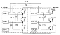
図1はこの発明の第の実施の形態を示す回路構成図、図2は磁気結合を説明するための説明図である。
図1はIGBTを3直列,2並列接続した1アーム分の構成を示し、IGBT(Q11〜Q23)とゲート駆動回路GDU11〜GDU23と磁気回路MCx,MC11〜MC23とから構成されている。
FIG. 1 is a circuit configuration diagram showing a first embodiment of the present invention, and FIG. 2 is an explanatory diagram for explaining magnetic coupling.
FIG. 1 shows a configuration for one arm in which three IGBTs are connected in series and two in parallel, and includes IGBTs (Q11 to Q23), gate drive circuits GDU11 to GDU23, and magnetic circuits MCx and MC11 to MC23.
磁気回路MCx,MC11〜MC23は、具体的には図2に示すように、磁気結合を行なう2素子のゲート線を同じ磁性体MGに巻数比1:1で巻き付けた構成であり、2素子のゲート電流Ig1,Ig2が等しい(Ig1=Ig2)時にゲート電流によって発生する磁束Φ1,Φ2が|Φ1|=|Φ2|となるようにし、Ig1とIg2が逆極性のときにΦ1とΦ2が逆極性となるようにしている。 Specifically, as shown in FIG. 2, the magnetic circuits MCx, MC11 to MC23 have a configuration in which two element gate lines for magnetic coupling are wound around the same magnetic body MG at a turns ratio of 1: 1. When the gate currents Ig1 and Ig2 are equal (Ig1 = Ig2), the magnetic fluxes Φ1 and Φ2 generated by the gate current are set to | Φ1 | = | Φ2 |. It is trying to become.
これにより、2素子のスイッチングタイミングが同時の場合には、Φ1とΦ2は同じレベルで逆極性となるため、互いに打ち消しあって磁気結合はしない。一方、タイミング差が生じた場合、例えばQ1が先にターンオフ(または、ターンオン)した時、すなわち、Ig1がIg2よりも先に流れたときΦ1≠Φ2となるため、磁気回路には|Φ1−Φ2|の磁束が発生し、磁気結合する。 As a result, when the switching timings of the two elements are the same, Φ1 and Φ2 are opposite in polarity at the same level, so they cancel each other and do not magnetically couple. On the other hand, when a timing difference occurs, for example, when Q1 is turned off (or turned on) first, that is, when Ig1 flows before Ig2, Φ1 ≠ Φ2, so that | Φ1-Φ2 A magnetic flux of | is generated and magnetically coupled.
このとき、それぞれのゲート線には等価的にインダクタンス分L1とL2が発生し、これらは|Φ1−Φ2|に比例する特性がある。すなわち、Ig1とIg2の差が大きいほど、L1とL2も大きくなる。また、L1,L2が増加するほどゲート線のインピーダンスが増加するため、Ig1とIg2が流れ難くなる。この動作により、Ig1とIg2の差分に応じて自動的にゲート線のインピーダンスが変化し、Ig1とIg2が一致するように動作することになる。 At this time, inductances L1 and L2 are equivalently generated in the respective gate lines, and these have characteristics proportional to | Φ1−Φ2 |. That is, L1 and L2 increase as the difference between Ig1 and Ig2 increases. Further, since the impedance of the gate line increases as L1 and L2 increase, Ig1 and Ig2 do not flow easily. With this operation, the impedance of the gate line automatically changes according to the difference between Ig1 and Ig2, and the operation is performed so that Ig1 and Ig2 match.
図1のIGBT(Q11〜Q13)とゲート駆動回路GDU11〜GDU13からなる直列回路1では、IGBTQ11とQ12のゲート線を磁気回路MC11により、IGBTQ12とQ13のゲート線を磁気回路MC12によりそれぞれ磁気結合させているため、3直列素子のスイッチングタイミングが一致し、印加される電圧をバランスさせることができる。 In the series circuit 1 composed of the IGBT (Q11 to Q13) and the gate drive circuits GDU11 to GDU13 in FIG. Therefore, the switching timings of the three series elements are matched, and the applied voltages can be balanced.
また、直列回路1と、IGBT(Q21〜Q23)とゲート駆動回路GDU11〜GDU23からなる直列回路2との間は、IGBTQ11とQ21のゲート線のみが磁気回路MCxによって磁気結合されている。このため、IGBTQ11とQ21のスイッチングタイミングが一致し、さらに直列回路2も直列回路1と同様に各素子が磁気結合されているため、結果的に3直列2並列の6素子全てのスイッチングタイミングが一致し、並列接続回路の電流バランスも均等にすることができる。なお、図1では直列接続の初段IGBTであるQ11とQ21を磁気結合したが、並列接続される直列回路間での磁気結合は、直列素子のいずれか1つの素子同士で行なえばよく、効果は同様である。 Further, between the series circuit 1 and the series circuit 2 including the IGBTs (Q21 to Q23) and the gate drive circuits GDU11 to GDU23, only the gate lines of the IGBTs Q11 and Q21 are magnetically coupled by the magnetic circuit MCx. For this reason, the switching timings of the IGBTs Q11 and Q21 are the same, and since the elements of the series circuit 2 are magnetically coupled in the same manner as the series circuit 1, the switching timings of all six elements in three series and two parallels are consequently equal. In addition, the current balance of the parallel connection circuit can be made uniform. In FIG. 1, Q11 and Q21, which are first-stage IGBTs connected in series, are magnetically coupled. However, magnetic coupling between series circuits connected in parallel may be performed by any one of the series elements. It is the same.
図3にこの発明の第2の実施の形態を示す。
これは、IGBTを3直列,3並列接続した1アーム分の回路例を示す。並列数が3以上の場合、図1の回路を拡張して並列接続間のIGBTQ11とQ21、およびQ21とQ31を互いに磁気結合させることも可能であるが、図3のように並列数nと同じn次巻線の磁気回路MCxにより磁気結合させることで、1つの磁気回路で複数の並列接続間を磁気結合でき、回路を簡素化することができる。
FIG. 3 shows a second embodiment of the present invention.
This shows a circuit example for one arm in which three IGBTs are connected in series and three in parallel. When the parallel number is 3 or more, it is possible to extend the circuit of FIG. 1 to magnetically couple the IGBTs Q11 and Q21 and Q21 and Q31 between the parallel connections to each other, but the same as the parallel number n as shown in FIG. By magnetically coupling by the magnetic circuit MCx of the n-order winding, a plurality of parallel connections can be magnetically coupled by one magnetic circuit, and the circuit can be simplified.
図4にこの発明の第3の実施の形態を示す。
これは、素子のゲート線とエミッタ線に流れる電流値が同じであることに着目し、ゲート線の代わりにエミッタ線を磁気結合させることで、素子のスイッチングタイミングを一致させるものである。回路動作等は図1に示すゲート線の場合と全く同様なので、説明は省略する。このような考え方を拡張させれば、ゲート線とエミッタ線の双方を磁気結合させることも可能で、上記と同様の効果を得ることができる。
FIG. 4 shows a third embodiment of the present invention.
This is based on the fact that the current values flowing in the gate line and the emitter line of the element are the same, and the switching timing of the element is matched by magnetically coupling the emitter line instead of the gate line. The circuit operation and the like are exactly the same as those of the gate line shown in FIG. If this concept is expanded, it is possible to magnetically couple both the gate line and the emitter line, and the same effect as described above can be obtained.
Q11〜Q33…IGBT(絶縁ゲートバイポーラトランジスタ)、GDU11〜GDU33…ゲート駆動回路、MCx,MC11〜MC32…磁気回路、MG…磁性体。
Q11 to Q33 ... IGBT (insulated gate bipolar transistor), GDU11 to GDU33 ... gate drive circuit, MCx, MC11 to MC32 ... magnetic circuit, MG ... magnetic material.
Claims (4)
前記直列接続回路内では、各段のゲート駆動回路と電圧駆動型半導体素子のゲート端子を接続するゲート線を互いに磁気結合させ、直列接続回路間では、各直列接続回路のいずれか1つの電圧駆動型半導体素子のゲート線どうしを互いに磁気結合させることを特徴とする半導体スイッチ回路。 A series-parallel connection circuit of voltage-driven semiconductor elements in which a plurality of series-connected circuits in which a plurality of voltage-driven semiconductor elements are connected in series are connected in parallel, and a voltage applicable for turning on / off each voltage-driven semiconductor element In a semiconductor switch circuit comprising a gate drive circuit for supplying a gate signal to a gate terminal of a drive type semiconductor element,
In the series connection circuit, a gate line connecting the gate drive circuit of each stage and the gate terminal of the voltage driven semiconductor element is magnetically coupled to each other, and any one of the series connection circuits is voltage driven between the series connection circuits. Switch circuit characterized in that the gate lines of the semiconductor device are magnetically coupled to each other.
The magnetic circuit that magnetically couples any one of the voltage-driven semiconductor elements of each of the series connection circuits has the same number of windings as the number of parallel connections. Semiconductor switch circuit.
Priority Applications (1)
| Application Number | Priority Date | Filing Date | Title |
|---|---|---|---|
| JP2004339413A JP4631409B2 (en) | 2004-11-24 | 2004-11-24 | Semiconductor switch circuit |
Applications Claiming Priority (1)
| Application Number | Priority Date | Filing Date | Title |
|---|---|---|---|
| JP2004339413A JP4631409B2 (en) | 2004-11-24 | 2004-11-24 | Semiconductor switch circuit |
Publications (2)
| Publication Number | Publication Date |
|---|---|
| JP2006149169A JP2006149169A (en) | 2006-06-08 |
| JP4631409B2 true JP4631409B2 (en) | 2011-02-16 |
Family
ID=36628199
Family Applications (1)
| Application Number | Title | Priority Date | Filing Date |
|---|---|---|---|
| JP2004339413A Expired - Fee Related JP4631409B2 (en) | 2004-11-24 | 2004-11-24 | Semiconductor switch circuit |
Country Status (1)
| Country | Link |
|---|---|
| JP (1) | JP4631409B2 (en) |
Families Citing this family (4)
| Publication number | Priority date | Publication date | Assignee | Title |
|---|---|---|---|---|
| JP2008043003A (en) * | 2006-08-03 | 2008-02-21 | Fuji Electric Systems Co Ltd | Gate drive unit of voltage-driven type semiconductor element |
| JP5786408B2 (en) * | 2011-03-31 | 2015-09-30 | 株式会社明電舎 | Voltage balance circuit of semiconductor switch circuit |
| CN103731127B (en) * | 2012-10-16 | 2016-12-21 | 通用电气公司 | Circuit for the electrical switch that Synchronization Control is connected in series |
| TW201703406A (en) * | 2015-04-14 | 2017-01-16 | 電源整合有限責任公司 | Switching device and power module |
Citations (8)
| Publication number | Priority date | Publication date | Assignee | Title |
|---|---|---|---|---|
| JPS62262086A (en) * | 1986-05-07 | 1987-11-14 | ソニー株式会社 | Switching circuit |
| JPH04125071A (en) * | 1990-09-17 | 1992-04-24 | Toshiba Corp | Power converter |
| JPH08266060A (en) * | 1995-03-20 | 1996-10-11 | Shimada Phys & Chem Ind Co Ltd | Inverter device |
| JPH10164843A (en) * | 1996-12-02 | 1998-06-19 | Toshiba Corp | Power conversion apparatus |
| JP2002204578A (en) * | 2001-01-09 | 2002-07-19 | Fuji Electric Co Ltd | Control device for series-connected voltage-driven semiconductor device |
| JP2003169464A (en) * | 2001-11-30 | 2003-06-13 | Fuji Electric Co Ltd | Controller for voltage-driven semiconductor devices connected in series |
| JP2004096829A (en) * | 2002-08-29 | 2004-03-25 | Fuji Electric Holdings Co Ltd | Controller of voltage-driven semiconductor device connected in parallel |
| JP2004215416A (en) * | 2003-01-06 | 2004-07-29 | Fuji Electric Holdings Co Ltd | Abnormality detection method for voltage-driven semiconductor element |
-
2004
- 2004-11-24 JP JP2004339413A patent/JP4631409B2/en not_active Expired - Fee Related
Patent Citations (8)
| Publication number | Priority date | Publication date | Assignee | Title |
|---|---|---|---|---|
| JPS62262086A (en) * | 1986-05-07 | 1987-11-14 | ソニー株式会社 | Switching circuit |
| JPH04125071A (en) * | 1990-09-17 | 1992-04-24 | Toshiba Corp | Power converter |
| JPH08266060A (en) * | 1995-03-20 | 1996-10-11 | Shimada Phys & Chem Ind Co Ltd | Inverter device |
| JPH10164843A (en) * | 1996-12-02 | 1998-06-19 | Toshiba Corp | Power conversion apparatus |
| JP2002204578A (en) * | 2001-01-09 | 2002-07-19 | Fuji Electric Co Ltd | Control device for series-connected voltage-driven semiconductor device |
| JP2003169464A (en) * | 2001-11-30 | 2003-06-13 | Fuji Electric Co Ltd | Controller for voltage-driven semiconductor devices connected in series |
| JP2004096829A (en) * | 2002-08-29 | 2004-03-25 | Fuji Electric Holdings Co Ltd | Controller of voltage-driven semiconductor device connected in parallel |
| JP2004215416A (en) * | 2003-01-06 | 2004-07-29 | Fuji Electric Holdings Co Ltd | Abnormality detection method for voltage-driven semiconductor element |
Also Published As
| Publication number | Publication date |
|---|---|
| JP2006149169A (en) | 2006-06-08 |
Similar Documents
| Publication | Publication Date | Title |
|---|---|---|
| JPWO2019038957A1 (en) | Control circuit and power conversion device | |
| US11489437B2 (en) | DC inverter/converter current balancing for paralleled phase leg switches | |
| JP4396036B2 (en) | Control device for voltage-driven semiconductor elements connected in series | |
| JP4675910B2 (en) | Inverter device | |
| JP4631409B2 (en) | Semiconductor switch circuit | |
| KR102055461B1 (en) | Power semiconductor circuit | |
| JP5348115B2 (en) | Load drive device | |
| JP3456836B2 (en) | Gate drive circuit | |
| US6049475A (en) | Power converting apparatus with drive signal path impedance increasing circuitry | |
| JP3767740B2 (en) | Control device for voltage-driven semiconductor elements connected in series | |
| US10587181B2 (en) | Power semiconductor device with built-in resistor between control electrode and control terminal, and power semiconductor drive system | |
| JPH0767320A (en) | Driving circuit for power element | |
| JP4026054B2 (en) | Control device for voltage-driven semiconductor elements connected in series | |
| US20190089349A1 (en) | Switching circuit | |
| JP4470616B2 (en) | Bidirectional switch drive power supply circuit | |
| JP3778351B2 (en) | Control device for voltage-driven semiconductor elements connected in series | |
| JP2020150739A (en) | Gate drive circuit | |
| JP4639687B2 (en) | Voltage variation suppression method for voltage-driven semiconductor devices | |
| JP6881399B2 (en) | Power semiconductor devices and power conversion devices | |
| JP7113182B2 (en) | inverter power supply | |
| JP4715346B2 (en) | Driving device for voltage-driven semiconductor elements connected in series | |
| JP4396059B2 (en) | Control device for voltage-driven semiconductor elements connected in series | |
| JPH0917660A (en) | Switch circuit | |
| JP3375255B2 (en) | Inverter circuit | |
| WO2023095244A1 (en) | Power conversion device |
Legal Events
| Date | Code | Title | Description |
|---|---|---|---|
| A621 | Written request for application examination |
Free format text: JAPANESE INTERMEDIATE CODE: A621 Effective date: 20071016 |
|
| TRDD | Decision of grant or rejection written | ||
| A977 | Report on retrieval |
Free format text: JAPANESE INTERMEDIATE CODE: A971007 Effective date: 20101014 |
|
| A01 | Written decision to grant a patent or to grant a registration (utility model) |
Free format text: JAPANESE INTERMEDIATE CODE: A01 Effective date: 20101019 |
|
| A01 | Written decision to grant a patent or to grant a registration (utility model) |
Free format text: JAPANESE INTERMEDIATE CODE: A01 |
|
| A61 | First payment of annual fees (during grant procedure) |
Free format text: JAPANESE INTERMEDIATE CODE: A61 Effective date: 20101101 |
|
| R150 | Certificate of patent or registration of utility model |
Free format text: JAPANESE INTERMEDIATE CODE: R150 |
|
| FPAY | Renewal fee payment (event date is renewal date of database) |
Free format text: PAYMENT UNTIL: 20131126 Year of fee payment: 3 |
|
| FPAY | Renewal fee payment (event date is renewal date of database) |
Free format text: PAYMENT UNTIL: 20131126 Year of fee payment: 3 |
|
| S533 | Written request for registration of change of name |
Free format text: JAPANESE INTERMEDIATE CODE: R313533 |
|
| FPAY | Renewal fee payment (event date is renewal date of database) |
Free format text: PAYMENT UNTIL: 20131126 Year of fee payment: 3 |
|
| R350 | Written notification of registration of transfer |
Free format text: JAPANESE INTERMEDIATE CODE: R350 |
|
| LAPS | Cancellation because of no payment of annual fees |