JP4627850B2 - Method for forming electrode of group III nitride semiconductor - Google Patents
Method for forming electrode of group III nitride semiconductor Download PDFInfo
- Publication number
- JP4627850B2 JP4627850B2 JP2000270989A JP2000270989A JP4627850B2 JP 4627850 B2 JP4627850 B2 JP 4627850B2 JP 2000270989 A JP2000270989 A JP 2000270989A JP 2000270989 A JP2000270989 A JP 2000270989A JP 4627850 B2 JP4627850 B2 JP 4627850B2
- Authority
- JP
- Japan
- Prior art keywords
- layer
- forming
- nitride semiconductor
- group iii
- electrode
- Prior art date
- Legal status (The legal status is an assumption and is not a legal conclusion. Google has not performed a legal analysis and makes no representation as to the accuracy of the status listed.)
- Expired - Lifetime
Links
Images


Landscapes
- Electrodes Of Semiconductors (AREA)
- Drying Of Semiconductors (AREA)
- Weting (AREA)
- Semiconductor Lasers (AREA)
Description
【0001】
【0002】
【発明の属する技術分野】
本発明は、III族窒化物からなる化合物半導体素子の電極の形成方法に関する。
【0003】
【従来の技術】
InxGayAlzN(ただしx+y+z=1、0≦x、y、z≦1)で表わされるIII族窒化物半導体は大きなエネルギーバンドギャップや高い熱安定性を有し、発光素子や高温デバイスを初めとして様々な応用展開が可能な有望な材料系である。特に発光素子としては、青〜緑の波長域で数cdの光出力を有する発光ダイオード(Light Emitting Diode;LED)が既に実用化されており、同材料系を用いたレーザダイオード(Laser Diode;LD)の実用化も間近である。
【0004】
これらのIII族窒化物系(以下、GaN系と記す)素子を実際の各種機器に搭載して使用する場合には、素子自体が消費する電力、動作する電圧を十分に低くする必要がある。
【0005】
特にGaN系LDの場合、GaN系LEDに比べて電流注入面積が小さく、p型電極部での電圧降下が素子全体の動作電圧に及ぼす影響を無視できない。従ってGaN系LDでは、このp型電極のオーミック化・低抵抗化が素子特性の向上に欠かせない。
【0006】
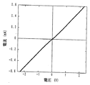
現在、GaN系素子に対するp型電極としてよく知られている電極構造としてはAu/Ni電極が挙げられる(なお本明細書内では、Au/Niという表記はNi層をAu層よりも先に形成し、Au層が電極の表面側に位置しているものとして統一する)。図1は、発明者らが試作したp型GaN上のAu/Niドット電極の電流−電圧特性を示したものである。
【0007】
図1に特性を示した電極は、図2に示した模式図のような構造で、サファイア基板201上にエピタキシャル成長したp型GaN層202(Mg不純物濃度2×1020cm-3、アクセプタ濃度3×1019cm-3)の表面を有機洗浄及び希釈塩酸にて処理したあと、電子ビーム(EB)真空蒸着装置でNiを15nm、Auを200nm成膜して角型電極203を形成してある。電極の大きさは一辺300μmの正方形、また電極間の間隔は50μmである。さらに、真空雰囲気中にて550℃で10分間熱処理を施し、電極構造を製作した。
【0008】
図1に示したとおり、Au/Ni電極はp型GaN層に対してオーミック特性を示す。また、電極−p型GaN層間の比コンタクト抵抗を測定したところ、5×10-3Ωcm2であった。
【0009】
【発明が解決しようとする課題】
しかしながら、発明者らが上記のAu/Ni電極をp型電極、p型GaN層をコンタクト層として適用したLD素子を製作し、その電気特性を測定したところ、素子内部のエピタキシャル層のシリーズ抵抗や前記の比コンタクト抵抗から予測されるよりもはるかに大きな動作電圧を示す結果が得られた。具体的には、電流を100mA注入時に予想される動作電圧は6〜7V程度であったが、実際に100mAの電流を注入してみると12〜13Vの動作電圧が確認された。
【0010】
動作電圧が予想値と違う原因を探るため、いくつかの解析を試みた。このうち、p型電極近傍に対するEBIC(Electron Beam Induced Current)解析を行ったところ、Au/Ni電極の特性がショットキー性を示していることが明らかになった。p型電極が本来のAu/Ni電極の特性を示さず、ショットキー性になっているために、p型電極部分で異常な電圧降下が生じ、その結果、素子の動作電圧を大きく増加させていたのである。
【0011】
上記のような解析結果を得て、発明者らは更に該LD素子のp型電極がショットキー性を示す起源がどこにあるのかを探るため、エピタキシャル成長やドライエッチング、電極形成などLDの製作プロセスを見直した。その結果、エピタキシャル成長後のGaN系半導体ウェハに電極やメサ構造などの素子構造を作り込む過程において、絶縁膜もしくはエッチングマスクなどの用途に用いられる誘電体膜が、上記のp型電極のショットキー性の起源となっていることを見出した。以下に、発明者らが用いたLD素子製作プロセスを、図18、図19を参照しながら順を追って記す。
【0012】
まず、GaN系LDの基板としてよく用いられるサファイア基板1501を用意し、その上に有機金属気相成長(MOCVD)法により、バッファ層1502、n型クラッド層1503、活性層1504、p型クラッド層1505、p型コンタクト層1506からなるGaN系半導体層構造を結晶成長した。その後、該GaN系半導体層構造表面の全面にわたって、SiO2層1507を成膜した(図18(a))。
【0013】
次に、フォトリソグラフィプロセス及びHFウェットエッチングプロセスによりSiO2層1507の一部を除去し、SiO2層の残した部分をエッチングマスクとして、RIE(Reactive Ion Etching)プロセスにより、前記GaN系半導体層構造をn型クラッド層1503の半ばまで掘り下げ、メサ構造を形成した(図18(b))。
【0014】
続いて、マスクとしたSiO2層1503をHFウェットエッチングにより完全に除去し、改めてSiO2層1508をメサ構造全体の上に形成した。更に、メサ上部及びメサ底部のSiO2層1508の一部をフォトリソグラフィプロセス及びHFウェットエッチングプロセスにより除去し、p型及びn型電極用の開口部を形成した(図19(a))。
【0015】
最後に、該開口部にそれぞれp型電極としてAu/Ni電極1509、n型電極としてAl/Ti電極1510を形成し、LD素子を製作した(図19(b))。
【0016】
上記に示したプロセスにより製作したLD素子は、図19(b)に明らかなように、絶縁基板上に形成されたメサ構造を有し、p型電極の電流注入部はいわゆる電極ストライプ構造を採っている。この形式のLD素子の場合、p型電極のうち電流注入部として機能するストライプ部分と接するp型コンタクト層表面(図19(b)のS部に示す)は、メサ構造形成時のマスク用及び電極の電流注入部形成用として、2度にわたってSiO2層により被覆されることになる(よって以下の文中では、上記プロセスを便宜的に2回被覆プロセスと記す)。
【0017】
さらに、発明者らは以下の検証実験を行った。図3には、図2に示した構造のAu/Niドット電極と同構造の電極をp型GaN層上に形成する前に、SiO2による被覆を1回及び2回実施した場合の電流−電圧特性を、それぞれ一点鎖線及び点線で示してある。なお図3には、比較のために図1にも示した事前にSiO2被覆していないAu/Ni電極の特性も同時に示している。
【0018】
図3に示したように、電極形成前にSiO2でp型GaN表面を2回被覆した場合の特性はオーミック性が損なわれ、電流−電圧特性が著しく劣化している。
SiO2被覆を1回に減らしても、やはり被覆しない場合と比べて特性の劣化とオーミック性の喪失がみられる。
【0019】
この検証実験の結果から、上記のLD素子製作プロセスにおけるp型電極のショットキー性は、2度にわたるSiO2のp型コンタクト層表面への被覆がもたらしたものであることことを明らかになった。
【0020】
上記の例では、すでに述べたようにサファイア基板上の電極ストライプLD素子についてプロセスを記したが、LD素子の素子の別の形式として、GaN基板上のLD素子を製作する場合、上記のプロセスで示したメサ構造の形成は不要だが電流注入部の形成時にはSiO2による被覆がプロセス上生じる。また、さらに別の素子の形式として、単純な電極ストライプ構造ではなくいわゆるリッジストライプ構造を有するLD素子を製作する場合には、リッジ部分を形成するドライエッチングプロセスにおいて、p型コンタクト層表面をSiO2などのマスクにより保護してエッチングを行う手法がよく用いられる。
【0021】
このように、III族窒化物半導体LD素子の製作プロセスにおいて、SiO2をはじめとする各種の誘電体膜を電極部分の一部を構成する絶縁層や、ドライエッチング時のエッチングマスクとして利用することはごく一般的に行われている。にも関わらず、誘電体膜をプロセス内で使用することが素子の特性に及ぼす影響や、またその影響を回避する手段等については従来論じられることがなかった。しかし、先に述べたようにGaN系LDにおいてp型電極部分の電圧降下が素子全体の動作電圧に占める割合は大きく、プロセスの違いにより図3に示したほどの特性差がp型電極部分に生じると、素子特性に与える影響は非常に大きい。よって、誘電体膜のプロセス内で使用する際にその影響を回避あるいは低減する手法を規定することは重要である。
【0022】
【課題を解決するための手段】
上記の問題点を鑑みると、p型電極異常を解決するには、素子製作プロセスにおいてp型電極形成前のSiO2誘電体によるp型GaN表面への被覆を行わないようにすれば良いのである。メサエッチ時にはレジストなどをマスク材料として用いたり、電極ストライプ形成時にウェットエッチングではなくリフトオフ法を用いるなど、代替のプロセスを適用することによってSiO2膜の被覆を回避することで、本発明が課題とすることが解決される。具体的には以下のような方法を用いる。
【0023】
本発明のIII族窒化物半導体の電極形成方法は、p型III族窒化物半導体の表面に接するPdからなる接触金属層をその少なくとも一部に含む電極を前記p型III族窒化物半導体の表面上に形成する方法であって、前記p型III族窒化物半導体の表面のうち前記接触金属層の形成箇所にフォトレジストを形成する工程と、前記フォトレジストの表面および前記p型III族窒化物半導体の表面を覆うように、SiO 2 からなる誘電体膜を形成する工程と、前記誘電体膜を形成する工程の後に、前記誘電体膜の表面上にMoを含む積層金属層を形成する工程と、前記フォトレジスト上の前記誘電体膜の一部を前記フォトレジストのリフトオフにより前記フォトレジストとともに除去することによって前記p型III族窒化物半導体の表面を露出させる工程と、前記p型III族窒化物半導体の露出表面に前記接触金属層を形成する工程と、を含み、前記p型III族窒化物半導体の表面を露出させる工程において、前記積層金属層の一部が前記誘電体膜とともに除去され、前記p型III族窒化物半導体の表面のうち前記接触金属層の形成箇所が、前記誘電体膜に接することなく前記電極を形成することを特徴とする。
【0024】
また、本発明のIII族窒化物半導体の電極形成方法は、前記フォトレジストを形成する工程の後に、前記フォトレジストをマスクとして前記p型III族窒化物半導体の一部を除去することによって、リッジを形成する工程を含むことを特徴とする。
【0026】
本発明のIII族窒化物半導体の電極形成方法は、前記接触金属層の形成箇所以外の前記p型III族窒化物半導体の表面部分を少なくとも除去することによって、前記接触金属層の形成箇所を頂部とするリッジを形成する工程を含むことを特徴とする。
【0028】
本発明のIII族窒化物半導体の電極形成方法は、p型III族窒化物半導体の表面に接するPdからなる接触金属層をその少なくとも一部に含む電極を前記p型III族窒化物半導体の表面上に形成する方法であって、前記p型III族窒化物半導体の表面上に第1のフォトレジストを形成する工程と、前記第1のフォトレジストをマスクとして前記p型III族窒化物半導体の一部を除去することによって、リッジを形成する工程と、前記リッジの頂部の前記接触金属層の形成箇所に第2のフォトレジストを形成する工程と、少なくとも前記第2のフォトレジストを覆うように、SiO 2 からなる誘電体膜を形成する工程と、前記誘電体膜を形成する工程の後に、前記誘電体膜の表面上にMoを含む積層金属層を形成する工程と、前記第2のフォトレジスト上の前記誘電体膜の一部を前記第2のフォトレジストのリフトオフにより前記第2のフォトレジストとともに除去することによって前記p型III族窒化物半導体の表面を露出させる工程と、前記p型III族窒化物半導体の露出表面に前記接触金属層を形成する工程と、を含み、前記p型III族窒化物半導体の表面を露出させる工程において、前記積層金属層の一部が前記誘電体膜とともに除去され、前記p型III族窒化物半導体の表面のうち前記接触金属層の形成箇所が、前記誘電体膜に接することなく前記電極を形成することを特徴とする。また、本発明のIII族窒化物半導体の電極形成方法は、p型III族窒化物半導体の表面に接するPdからなる接触金属層をその少なくとも一部に含む電極を前記p型III族窒化物半導体の表面上に形成する方法であって、前記p型III族窒化物半導体の表面上にフォトレジストを形成する工程と、前記フォトレジストをマスクとして前記p型III族窒化物半導体の一部を除去することによってリッジを形成する工程と、少なくとも前記フォトレジストを覆うように、SiO 2 からなる誘電体膜を形成する工程と、前記フォトレジスト上の前記誘電体膜の一部を前記フォトレジストのリフトオフにより前記フォトレジストとともに除去することによって前記p型III族窒化物半導体の表面を露出させる工程と、前記p型III族窒化物半導体の露出表面に前記接触金属層を形成する工程と、を含み、前記p型III族窒化物半導体の表面のうち前記接触金属層の形成箇所が、前記誘電体膜に接することなく前記電極を形成することを特徴とする。また、本発明のIII族窒化物半導体の電極形成方法は、前記誘電体膜を形成する工程の後に、前記誘電体膜の表面上にMoを含む積層金属層を形成する工程を含み、前記p型III族窒化物半導体の表面を露出させる工程において、前記積層金属層の一部が前記誘電体膜とともに除去されることを特徴とする。
【0030】
本発明のIII族窒化物半導体の電極形成方法は、前記p型III族窒化物半導体は、Mgをドーパントとして含有するAlGaInNであることを特徴とする。
【0031】
本発明のIII族窒化物半導体の電極形成方法は、前記積層金属層が、Mo層、またはMo層とAu層との積層体であることを特徴とする。
【0035】
なお、図3で示したSiO2被覆を1回もしくは2回施した後に形成されたp型電極とp型コンタクト層の界面に対し、SIMS(二次イオン質量分析装置)やAES(オージェ電子分光分析装置)による解析を試みたが、誘電体が残留している痕跡は見られなかった。図3で示した電極のショットキー性は、SiO2のエッチング不足によるp型GaN表面への残留が原因というわけではないと思われる。むしろ、SiO2の被覆によりp型GaN表面が何らかの変成を起こした可能性がるものと考えられる。
【0036】
また、上記の例ではp型コンタクト層表面を被覆する材料としてSiO2のみを取り上げているが、前述のp型電極特性異常はSiO2に限らず、他の誘電体を用いても発生する。発明者らはSiO2の他に、Al2O3、TiO2、SiN、AlN、SiOx、SiON、ZrO2などを含む酸化物あるいは窒化物誘電体で、上記と同様のp型電極特性異常が発生することを確認した。
【0037】
また、上記の例ではp型電極としてAu/Ni電極を用いているが、前述のp型電極特性異常はp型コンタクト層に接する側の金属がNiの場合だけでなく、他の金属からなる場合でも発生する。発明者らはAu/Ni電極の他に、Au/Pd電極やAu/Pt電極、Au/Co電極などで、上記と同様にp型電極の特性に異常を来たすことを確認した。
【0038】
また、p型コンタクト層の材質は、GaN系半導体素子のp型コンタクト層としてよく用いられるp型GaNのほかに、AlGaNやInGaN、AlInGaNを用いても、前述のp型電極特性異常が発生することが確認できた。
【0039】
【発明の実施の形態】
以下に示す各実施例は、前記の2回被覆プロセスを手直しし、LD素子の特性改善を図るために実施した各種のLD素子製作プロセスである。なお、各実施例において製作したLD素子のp型電極における電流注入部の大きさは、特性の比較のため、すべて幅10μm、長さ500μmの長方形に統一した。
(参考例1)図4及び5は、本発明の第1の実施例に係るGaN系LD素子の断面構造を、製作プロセスを追って模式的に示したものである。
【0040】
最初に、サファイア基板401上に、GaNバッファ層402、n型AlGaNクラッド層403、MQW(多重量子井戸構造)活性層404、p型AlGaNクラッド層405、p型GaNコンタクト層406をMOCVD法により順次エピタキシャル成長し、GaN系半導体積層構造を製作する。続いて該積層構造上にフォトレジストによるドライエッチングマスク407を形成した後、該マスク407で被覆されていない部分を、RIEによりn型クラッド層403の半ばまで掘り下げ、メサ構造を形成する。(図4(a))。
【0041】
次に、マスク407を完全に除去した後、メサ上部にフォトレジストによるストライプパターン408を形成する。さらに、その上からメサ構造全面にわたってSiO2層409を成膜する(図4(b))。
【0042】
次に、ストライプパターン408及びその直上に形成されたSiO2層409の一部をリフトオフプロセスにより除去し、続いてメサ構造の底部に位置するSiO2層409の一部をフォトリソグラフィプロセス及びHFウェットエッチングプロセスにより除去し、SiO2層408に開口部を設ける(図5(a))。なおこの際、リフトオフプロセス特有の現象として、開口部端のSiO2が若干捲れ上がる場合があるが、素子の特性には特に影響は与えないので問題にしなくてよい。
【0043】
最後に、開口部を形成するために形成したフォトレジストマスク410を除去した後、メサ上部及びメサ底部のSiO2開口部にそれぞれp型電極としてAu/Ni電極411、n型電極としてAl/Ti電極412を形成し、LD素子を完成する(図5(b))
本実施例のプロセスでは、先に示した2回被覆プロセスから、メサ構造形成のためのRIEマスクとして使用する材料をSiO2からフォトレジストに変更し、また電流注入用のストライプ部を形成するためにフォトレジストをリフトオフする工程を採用している。このようなプロセスを実施することにより、p型電極のうち電流注入部にあたる部分のp型GaNコンタクト層表面へのSiO2被覆の履歴を、まったく無くすことができる。
【0044】
本実施例の製作プロセスにより製作されたLD素子と、前記の2回被覆プロセスによるLD素子の動作電圧を比較したところ、注入電流100mAの時それぞれ6.5Vと12Vとなった。これは、本実施例のLD素子製作プロセスの効果が明確に現れた結果であり、p型電極の電流注入部にSiO2被覆の履歴を付けないことがLD素子の動作電圧低減に非常に有効であることを示すものである。
(参考例2)本発明の第2の実施例は、第1の実施例で示したようなp型電極の電流注入部へのSiO2被覆履歴がないLD素子を、第1の実施例とは異なるプロセスで実現したものである。
【0045】
図6及び図7に、本発明の第2の実施例に係るGaN系LD素子の断面構造を、製作プロセスを追って模式的に示す。
【0046】
最初に、サファイア基板601上に、GaNバッファ層602、n型AlGaNクラッド層603、MQW活性層604、p型AlGaNクラッド層605、p型GaNコンタクト層606をMOCVD法により順次エピタキシャル成長し、GaN系半導体積層構造を製作する。続いて、該半導体積層構造の上から全面にわたり、Ni層607、Au層608を成膜する(図6(a))。
【0047】
次に、Ni層607、Au層608を電流注入部を残して王水、希硝酸にてウェットエッチした後、フォトレジストによるドライエッチングマスク609を形成し、該マスク609で被覆されていない部分を、RIEによりn型クラッド層603の半ばまで掘り下げ、メサ構造を形成する(図6(b))。
【0048】
メサ構造形成後、マスク609を完全に除去し、改めてフォトリソグラフィプロセスにより、メサ底部に開口部を有するフォトレジストパターン610を形成する(図7(a))。
【0049】
最後に、メサ構造上面から全面にわたってTi層611、Al層612を順次成膜した後、フォトレジストパターン610をリフトオフしてAi/Ti電極を形成し、LD素子を完成する(図7(b))。
【0050】
本実施例で示したプロセスでは、第1の実施例と異なり、p型電極のうち電流注入部にあたる部分の形成には、フォトレジストによるリフトオフではなく、電極の直接成膜及び電極エッチングという工程を使用している。しかし、該部分のSiO2による被覆が無いという点では共通しており、製作したLD素子の特性に関しても、100mA通電時に6.7Vと、第1の実施例とほぼ同様の電流−電圧特性が得られた。
【0051】
なお、本実施例においては、p型電極の電流注入部の形成方法として酸によるウェットエッチングを用いたが、電流注入部の形成方法としてはこれに限らず、フォトレジストによるリフトオフ法を用いても良い。
【0052】
すなわち、図8に基づいて説明すると、上記の実施例2と同様にサファイア基板601上に、GaNバッファ層602、n型AlGaNクラッド層603、MQW活性層604、p型AlGaNクラッド層605、p型GaNコンタクト層606をMOCVD法により順次エピタキシャル成長し、p型GaNコンタクト層606上面に、開口部を有するフォトレジストパターン613を形成する。その後、前記開口部を含む全面にNi層607、Au層608を成膜する(図8(a))。
【0053】
次に、フォトレジストパターン613と、Ni層607、Au層608のうちフォトレジストパターン613上に形成された分をリフトオフすることで、ストライプ状のp型電極部が形成される(図8(b))。
【0054】
このようにしてp型電極部を形成した場合には、電極部の構造は上記の第2の実施例とほぼ同じとなるが、電極の形成前にp型GaNコンタクト層表面をフォトレジストが一回被覆するため、厳密には第2の実施例とはプロセスが異なる。しかしながら、SiO2による被覆とは異なり、フォトレジストによる被覆は、電極の特性になんら影響を与えないので、製作したLD素子の特性は、第2の実施例によるLD素子と概略同じ特性を示す。(参考例3)図9及び図10には、本発明の第3の実施例に係るGaN系LD素子の断面構造を、プロセスを追って模式的に示す。
【0055】
最初に、サファイア基板801上に、GaNバッファ層802、n型AlGaNクラッド層803、MQW活性層804、p型AlGaNクラッド層805、p型GaNコンタクト層806をMOCVD法により順次エピタキシャル成長し、GaN系半導体積層構造を製作する。続いて該積層構造上にフォトレジストによるドライエッチングマスク807を形成した後、該マスク807で被覆されていない部分を、RIEによりn型クラッド層803の半ばまで掘り下げ、メサ構造を形成する。(図9(a))。
【0056】
次に、マスク807を完全に除去した後、メサ上部にフォトレジストによるストライプパターン808を形成する。さらに、その上からメサ構造全面にわたってSiO2層809、Mo層810、Au層811を成膜する(図9(b))。
【0057】
次に、ストライプパターン808及びその直上に形成されたSiO2層809、Mo層810、Au層811の一部をリフトオフプロセスにより除去し、続いてメサ構造の底部に位置するSiO2層809、Mo層810、Au層811の一部をフォトリソグラフィプロセス及びウェットエッチングプロセスにより除去し、SiO2層809に開口部を設ける(図10(a))。なおこの際、リフトオフプロセス特有の現象として、開口部端のSiO2が若干捲れ上がる場合があるが、素子の特性には特に影響は与えないので問題にしなくてよい。
【0058】
最後に、開口部を形成するために形成したフォトレジストマスクを除去した後、メサ上部及びメサ底部のSiO2開口部にそれぞれp型電極としてAu/Pd電極812、n型電極としてAl/Ti電極813を形成し、LD素子を完成する(図10(b))
本実施例のプロセスでは、第1及び第2の実施例と同様に、p型電極のうち電流注入部になる部分のp型GaNコンタクト層表面へのSiO2被覆履歴をまったく無くすることで、電極部分での良好なオーミック性が達成されている。
【0059】
なお、本実施例の製作プロセスにより製作されたLD素子の注入電流100mAの時の動作電圧は5.5Vとなり、第1及び第2の実施例と比較して大幅に低くなった。これはp型電極をAu/Ni電極からAu/Pd電極に変更したことの効果が現れた結果であって、Au/Pd電極はAu/Ni電極と比較して、より低抵抗なオーミック電極をもたらすためである。
【0060】
また、本実施例においては、SiO2層809の上に、Mo層810及びAu層811を成膜しているが、これもまた本実施例がp電極としてAu/Pd電極を採用している故である。図10(b)に示したAu/Pd電極のうち、電流注入部を除いた部分はPdとAu/Mo/SiO2積層部が接している。第1及び第2の実施例と同じようにMo層810、Au層811を成膜しなければ、Pd層はSiO2層と直接接触することになる。しかしながら、Pdは本質的にSiO2との密着性が極めて弱いという性質を有しているため、Pd層がSiO2層と直接接触するように形成するとp型電極が剥がれてしまう。これを避けるため、本実施例ではSiO2と密着性の良好なMo層をスペーサ層として用いている。
【0061】
本実施例の製作プロセスは、また、次に述べるように、SiO2とPd層と直接接触する領域が、極めて少なく、事実上p電極が剥がれる事がない構造を、簡便に製作できるという効果も有している。
【0062】
即ち、本実施例の製作プロセスに依らずに、例えば、SiO2層に開口部を設けてから、該開口部をフォトレジスト等でマスキングした後にMo層を形成し、その後リフトオフプロセスより、該開口部上のMo層を除去する場合は、該開口部上のみに正確にフォトレジストマスクを形成する事が必要であるが、実際には、形成するマスクの位置、幅には、0.1〜0.5μm程度のばらつきが生じることが不可避であり、このようなフォトレジストマスクの形成は非常に困難である。また、SiO2層、Mo層、Au層を形成してから、Au層上に開口部を有するフォトレジストマスクを形成し、ウェットエッチングにより、AuやMoに開口部を設ける場合では、サイドエッチングの影響で、所望の開口部幅よりも、実際にエッチングされるAuやMoの領域の幅が大きくなってしまい、かつその幅の制御が非常に困難であるため、やはり、本実施例による製作プロセスの場合の様に、該開口部以外のSiO2層上を、完全にMo層、Au層で覆う構造の形成は困難である。
【0063】
これに対し、本実施例の製作プロセスにおいては、SiO2膜809に、p型電極のうちの電流注入部となる開口部を形成するにあたって、ストラプパターン808上に、SiO2膜809、Mo層810、Au層811を形成してから、ストラプパターン808、SiO2膜809、Mo層810、Au層811をリフトオフプロセスにより、同時に除去している。このため、該開口部には、Mo層810、Au層811が全く被っておらず、逆に、該開口部以外のSiO2層上は、完全にMo層810、Au層811で覆われている。このため、上にPd層を形成してやる際に、SiO2とPd層と直接接触するのは、開口部でSiO2の断面が露出している極めて微小な領域に限られ、事実上、p電極が剥がれる事はない。
【0064】
また、Au層811の役割は、Mo層積層後のリフトオフプロセスやフォトリソグラフィプロセスの間、Mo層810の表面を保護することにある。
【0065】
また、本実施例のLD素子を形成する過程においては、上記のようにp型電極のストライプ状の電流注入部を形成する手法として、第1の実施例と同様にSiO2層のリフトオフプロセスを用いているが、第2の実施例に記載したプロセスと同様にp型電極のウェットエッチングを用いて形成しても、本実施例とほぼ同等の特性を有する素子を得ることができ、なんら問題はない。なお、p型電極の形成手法としてウェットエッチングプロセスを用いる場合には、上記のうちSiO2層809を成膜する必要がないので、Mo層810、Au層811も不要であることは言うまでもない。
(参考例4)図11、図12及び図13には、本発明の第4の実施例に係るGaN系LD素子の断面構造を、プロセスを追って模式的に示す。
【0066】
最初に、サファイア基板1001上に、GaNバッファ層1002、n型AlGaNクラッド層1003、MQW活性層1004、p型AlGaNクラッド層1005、p型GaNコンタクト層1006をMOCVD法により順次エピタキシャル成長し、GaN系半導体積層構造1000を製作する。続いて該コンタクト層1006表面の一部に、フォトレジストによるエッチングマスクパターン1007を形成した後、該マスクパターン1007で被覆されていない部分を、RIEによりp型クラッド層1005の半ばまで掘り下げ、リッジ構造を形成する。(図11(a))。
【0067】
続いて、マスクパターン1007を完全に除去した後、該リッジ構造を含む半導体積層構造1000の上面の一部に、フォトレジストによるドライエッチングマスク1008を形成した後、該マスク1008で被覆されていない部分を、RIEによりn型クラッド層1003の半ばまで掘り下げ、メサ構造を形成する。
(図11(b))。
【0068】
次に、マスク1008を完全に除去し、リッジ上部にフォトレジストによるストライプパターン1009を形成する。さらに、その上からメサ構造全面にわたってSiO2層1010、Mo層1011、Au層1012を成膜する(図12(a))。
【0069】
次に、ストライプパターン1009及びその直上に形成されたSiO2層1010、Mo層1011、Au層1012の一部をリフトオフプロセスにより除去し、続いてメサ構造の底部に位置するSiO2層1010、Mo層1011、Au層1012の一部をフォトリソグラフィプロセス及びウェットエッチングプロセスにより除去し、SiO2層1010に開口部を設ける(図12(b))。なおこの際、リフトオフプロセス特有の現象として、開口部端のSiO2が若干捲れ上がる場合があるが、素子の特性には特に影響は与えないので問題にしなくてよい。
【0070】
最後に、開口部を形成するために形成したフォトレジストマスクを除去した後、メサ上部及びメサ底部のSiO2開口部にそれぞれp型電極としてAu/Pd電極1013、n型電極としてAl/Ti電極1014を形成し、LD素子を完成する(図13)。
【0071】
本実施例のプロセスでは、第1〜第3の実施例と同様に、p型電極のうち電流注入部になる部分のp型GaNコンタクト層表面へのSiO2被覆履歴をまったく無くすることで、電極部分での良好なオーミック性が達成されている。
【0072】
なお、本実施例のLD素子はリッジ構造を採っており、同種のp型電極を有する第3の実施例と比較して電流−電圧特性が改善されている。このため、注入電流100mAの時の動作電圧は5.3Vとなり、第3の実施例よりも更に低くなった。
【0073】
また、本実施例のLD素子を形成する過程においては、上記のようにp型電極のストライプ状の電流注入部を形成する手法として、第1の実施例と同様にSiO2層のリフトオフプロセスを用いているが、第2の実施例に記載したプロセスと同様にp型電極のウェットエッチングを用いて形成しても、本実施例とほぼ同等の特性を有する素子を得ることができ、なんら問題はない。なお、p型電極の形成手法としてウェットエッチングプロセスを用いる場合には、上記のうちSiO2層1010を成膜する必要がないので、Mo層1011、Au層1012も不要であることは言うまでもない。
【0074】
また、本実施例におけるp型電極としては、第3の実施例と同様にAu/Pd電極を用いているが、第1及び第2の実施例と同様にAu/Ni電極を用いても、本発明の素子製作プロセスの特徴が損なわれるものではない。この場合、素子への注入電流が100mAの時の動作電圧は6.5Vとなる。
(実施例5)
図14及び図15には、本発明の第5の実施例に係るGaN系LD素子の断面構造を、プロセスを追って模式的に示す。
【0075】
最初に、n型GaN基板1301上に、n型GaNバッファ層1302、n型AlGaNクラッド層1303、MQW活性層1304、p型AlGaNクラッド層1305、p型GaNコンタクト層1306をMOCVD法により順次エピタキシャル成長し、GaN系半導体積層構造1300を製作する。続いて該コンタクト層1306表面の一部に、フォトレジストによるエッチングマスクパターン1307を形成した後、該マスクパターン1307で被覆されていない部分を、RIEによりp型クラッド層1305の半ばまで掘り下げ、リッジ構造を形成する。(図14(a))。
【0076】
次に、マスクパターン1307を完全に除去した後、リッジ上部にフォトレジストによるストライプ状の電流注入パターン1308を形成する。さらに、その上からリッジ構造全面にわたってSiO2層1309、Mo層1310、Au層1311を成膜する(図14(b))。
【0077】
最後に、ストライプパターン1308及びその直上に形成されたSiO2層1309、Mo層1310、Au層1311の一部をリフトオフプロセスにより除去し、リッジ構造上面にp型電極の電流注入部となる開口部を形成する。なおこの際、リフトオフプロセス特有の現象として、開口部端のSiO2が若干捲れ上がる場合があるが、素子の特性には特に影響は与えないので問題にしなくてよい。
【0078】
その後、該開口部を含むリッジ上面及び基板1301裏面にそれぞれp型電極としてAu/Pd電極1312、n型電極としてAl/Ti電極1313を形成し、LD素子を完成する(図15)。
【0079】
本実施例のプロセスでは、第1〜第4の実施例とは異なり、LD素子の基板として絶縁性のサファイアではなく、導電性のGaN基板を用いている。このため、n型電極を基板裏面より直接取ることが可能で、第1〜第4の実施例で必要であったRIEによるメサ構造の形成が不要になっている。
【0080】
本実施例においても、第3及び第4の実施例と同様、p型電極としてAu/Pd電極を用いているが、素子構造としてリッジ構造をとっており、またGaN基板を使用することで基板とその上のエピタキシャル層の格子不整合及び格子欠陥の発生が抑止され、その結果として第4の実施例よりもさらに電流−電圧特性が改善されている。そのため注入電流100mAの時の動作電圧は5.1Vとなり、第4の実施例と比較して低くなった。
【0081】
また、本実施例のLD素子を形成する過程においては、上記のようにp型電極のストライプ状の電流注入部を形成する手法として、第1の実施例と同様にSiO2層のリフトオフプロセスを用いているが、第2の実施例に記載したプロセスと同様にp型電極のウェットエッチングを用いて形成しても、本実施例とほぼ同等の特性を有する素子を得ることができ、なんら問題はない。なお、p型電極の形成手法としてウェットエッチングプロセスを用いる場合には、上記のうちSiO2層1309を成膜する必要がないので、Mo層1310、Au層1311も不要であることは言うまでもない。
【0082】
また、本実施例におけるp型電極としては、第3及び第4の実施例と同様にAu/Pd電極を用いているが、第1及び第2の実施例と同様にAu/Ni電極を用いても、本発明の素子製作プロセスの特徴が損なわれるものではない。この場合、素子への注入電流が100mAの時の動作電圧は6.3Vとなる。
【0083】
また、本実施例のLD素子は第4の実施例と同様にリッジ構造を有しているが、第3の実施例のようにリッジ構造を有していない場合でも、本発明の素子製作プロセスの特徴が損なわれるものではない。但しこの場合、リッジ構造によるp型電極直下部での電流狭窄効果は失われるため、LD素子の特性は本実施例のLD素子よりも若干悪くなり、素子への注入電流が100mAの時の動作電圧は6.5Vとなる。
【0084】
なお、GaN基板の面方位に関しては、GaN基板の{0001}面、{1−100}面、{11−20}面、{1−101}面、{11−22}面、{01−12}面を用いることが好ましい。また、各面方位から±2度程度の面ずれが生じても、素子特性にはほとんど影響を及ぼさないことが確認できた。
【0085】
(実施例6)
図16と図17には、本発明の第6の実施例に係るGaN系LD素子の断面構造を、模式的に示す。本実施例は、先述の、本発明の第1の実施例に、本発明の第4の実施例で用いた、リッジストライプ形成プロセスを組み合わせたものである。
【0086】
最初に、サファイア基板1401上に、GaNバッファ層1402、n型AlGaNクラッド層1403、MQW活性層1404、p型AlGaNクラッド層1405、p型GaNコンタクト層1406を、MOCVD法により順次エピタキシャル成長し、GaN系半導体積層構造を製作する。続いて、該積層構造上にフォトレジストストライプパターン1408を形成した後、該マスクで被覆されていない部分を、RIEによりp型AlGaNクラッド層1405の半ばまで掘り下げ、リッジ構造を形成する。(図16(a))
次に、マスクを残したまま、SiO2層1409、Mo層1411、Au層1412を成膜する。次に、前記フォトレジストストライプパターン1408、及びその直上に形成されたSiO2層1409、Mo層1411、Au層1412の一部を、リフトオフプロセスにより除去し、SiO2層1409に開口部を設ける。(図16(b))
次に、該SiO2層1409の開口部とその近傍のAu層1412上に、p型電極としてAu/Pd電極1413を形成する。続いて、該Au/Pd電極1413およびその近傍のAu層1412上に、フォトレジストによるドライエッチングマスク1407を形成した後、まず、王水によるウェットエッチングにより、該マスクで被覆されていない部分のAu層1412を除去し、その後、RIEにより、Mo層1411、及びSiO2層1409を除去し、更にRIEにより、GaN系半導体積層構造をn型AlGaNクラッド層1403の半ばまで掘り下げ、メサ構造を形成する。(図17(a))
最後に、RIEにより露出したn型AlGaNクラッド層1403の表面に、n型電極としてAl/Ti電極1410を形成し、LD素子を完成する。(図17(b))
本実施例のプロセスでは、第4の実施例と同様にリッジ構造を有しているが、第4の実施例の場合と異なり、リッジ形成後に、ドライエッチングマスクを除去する事なくSiO2層を被覆し、リフトオフによりp型GaNコンタクト層上のドライエッチングマスク及びSiO2層を除去する。このため、工程数が減り、より簡便に素子化する事ができる。また、p型電極をリッジ上面に形成するためのフォトレジストによるストライプパターンを形成する必要がないので、リッジ上面に該ストライプパターンをアライメントする際の位置、線幅のばらつきに起因する特性のばらつきも、全くない。
【0087】
上記の6つの実施例では、p型コンタクト層に接触する金属としてNi、Pdを示したが、発明者らの検討によれば、他にもPt、Ru、Rh、Os、Ir、Co、Crといった金属で、本明細書で示したような誘電体膜被覆の影響があることが分かった。従ってこれらの金属をGaN系半導体素子のp型電極として用いる場合、本発明の製作プロセスを実施することで、電極部分での電圧降下の低減に大きく寄与する。
【0088】
また上記の6つの実施例では、p型コンタクト層としてp型GaNを用いて説明したが、発明者らの検討によれば、本発明の効果はGaNに限定されず、InxGayAlzN(ただしx+y+z=1、0≦x、y、z≦1)なる組成を満たし、Mgをドーパントとするコンタクト層であれば、有効であることが分かった。
【0089】
また、上記の6つの実施例では、素子製作プロセスでp型電極の電流注入部が被覆を避けなければならない誘電体膜としてSiO2膜を対象としたが、発明者らの検討によれば、SiO2に限らず、Al2O3,TiO2,SiN,AlN,SiOx,SiON,ZrO2のいずれかを含む酸化物あるいは窒化物誘電体による被覆に関しても、電流−電圧特性への影響が確認された。よってSiO2以外のこれらの誘電体に関しても、上記に示したようなp型電極の電流注入部への被覆を回避する製作プロセスは非常に有益である。
【0090】
また、上記の6つの実施例では、LD素子の基板としてサファイア基板及びn型GaN基板を用いているが、いずれの基板を用いる場合でも、本発明の特徴であるp型電極の電流注入部に対し電極を形成する前の誘電体被覆を回避する素子製作プロセスが有効であることは、既に示した通りである。従って、上記の5つの実施例においてサファイア基板をn型GaN基板に置き換えても、あるいは逆にn型GaN基板をサファイア基板に置き換えても、素子構造や電流−電圧特性に違いはあるが、本発明の素子製作プロセスによるp型電極の低抵抗化は確実に達成される。
【0091】
また、上記の実施例1〜4及び6では、n型電極を、n型AlGaNクラッド層の上に設けているが、n型GaNバッファ層とn型AlGaNクラッド層の間にn型コンタクト層が挿入された構造とし、n型電極をn型コンタクト層の上に設けても、何ら問題はない。
【0092】
また、実施例3、4、5、及び6に於いては、SiO2との密着性が良好なスペーサ層として、Moを用いているが、Al、Mg、W、Ni、Fe、Cr、Ta、V、Zr、Tiなどを少なくとも一種類用いても、同様の効果が得られる。
【0093】
【発明の効果】
本発明によれば、LDをはじめとするGaN系半導体素子において、p型電極の電流注入部と接するGaNコンタクト層表面を、電極金属の形成前に誘電体膜で被覆しないことにより、電極部での電流−電圧特性を良好に保ち、その結果として素子の動作電圧が大幅に低減される。
【図面の簡単な説明】
【図1】p型GaNに対するAu/Ni電極の、電流−電圧特性を示す模式図である。
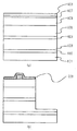
【図2】第1図に特性を示した電極構造の、概観を示す斜視図である。
【図3】電極の形成前のp型GaNコンタクト層表面へのSiO2膜被覆回数を変化させた場合の、各Au/Ni電極の電流−電圧特性を示す模式図である。
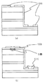
【図4】本発明の第1の実施例のLD素子製作プロセスを、LD素子断面構造により順を追って示した模式図である。
【図5】本発明の第1の実施例のLD素子製作プロセスを、LD素子断面構造により順を追って示した模式図である。
【図6】本発明の第2の実施例のLD素子製作プロセスを、LD素子断面構造により順を追って示した模式図である。
【図7】本発明の第2の実施例のLD素子製作プロセスを、LD素子断面構造により順を追って示した模式図である。
【図8】本発明の第2の実施例の変形例である。
【図9】本発明の第3の実施例のLD素子製作プロセスを、LD素子断面構造により順を追って示した模式図である。
【図10】本発明の第3の実施例のLD素子製作プロセスを、LD素子断面構造により順を追って示した模式図である。
【図11】本発明の第4の実施例のLD素子製作プロセスを、LD素子断面構造により順を追って示した模式図である。
【図12】本発明の第4の実施例のLD素子製作プロセスを、LD素子断面構造により順を追って示した模式図である。
【図13】本発明の第4の実施例のLD素子製作プロセスを、LD素子断面構造により順を追って示した模式図である。
【図14】本発明の第5の実施例のLD素子製作プロセスを、LD素子断面構造により順を追って示した模式図である。
【図15】本発明の第5の実施例のLD素子製作プロセスを、LD素子断面構造により順を追って示した模式図である。
【図16】本発明の第6の実施例のLD素子作成プロセスを、LD素子断面構造により順を追って示した模式図である。
【図17】本発明の第6の実施例のLD素子作成プロセスを、LD素子断面構造により順を追って示した模式図である。
【図18】本発明に対する従来例のLD素子製作プロセスを、LD素子断面構造により順を追って示した模式図である。
【図19】本発明に対する従来例のLD素子製作プロセスを、LD素子断面構造により順を追って示した模式図である。
【符号の説明】
201…サファイア基板
202…p型GaN層
203…Au/Ni電極
401、601、801、1001、1401、1501…サファイア基板
402、602、802、1002、1402、1502…GaNバッファ層
403、603、803、1003、1403、1303、1503…n型AlGaNクラッド層
404、604、804、1004、1304、1404、1504…MQW活性層
405、605、805、1005、1305、1405、1505…p型AlGaNクラッド層
406、606、806、1006、1306、1406、1506…p型GaNコンタクト層
407、807、1008、1407…ドライエッチングマスク
408、808、1009、1408…フォトレジストストライプパターン
409、809、1010、1409…SiO2層
410…フォトレジストマスク
411…Au/Ni電極
412、813、1014、1313、1410、1510…Al/Ti電極
607…Ni層
608…Au層
609…ドライエッチングマスク
610、613…フォトレジストパターン
611…Ti層
612…Al層
810、1011、1411…Mo層
811、1012、1412…Au層
812、1013、1312、1413…Au/Pd電極
1007…リッジ構造形成用ドライエッチングマスク
1301…n型GaN基板
1302…n型GaNバッファ層
1307…ドライエッチングマスク
1308…ストライプ状電流注入パターン
1309…SiO2層
1310…Mo層
1311…Au層
1507…SiO2層
1508…SiO2層
1509…Au/Ni電極[0001]
[0002]
BACKGROUND OF THE INVENTION
The present invention relates to a method for forming an electrode of a compound semiconductor element made of a group III nitride.
[0003]
[Prior art]
InxGayAlzGroup III nitride semiconductors represented by N (where x + y + z = 1, 0 ≦ x, y, z ≦ 1) have a large energy band gap and high thermal stability, and are used in various applications including light-emitting devices and high-temperature devices. It is a promising material system that can be developed. In particular, as a light emitting element, a light emitting diode (LED) having a light output of several cd in a blue to green wavelength region has already been put into practical use, and a laser diode (Laser Diode; LD) using the same material system is already used. ) Is coming soon.
[0004]
When these group III nitride (hereinafter referred to as GaN) elements are used in various actual devices, it is necessary to sufficiently reduce the power consumed by the elements themselves and the operating voltage.
[0005]
In particular, in the case of a GaN-based LD, the current injection area is smaller than that of a GaN-based LED, and the influence of the voltage drop at the p-type electrode portion on the operating voltage of the entire device cannot be ignored. Therefore, in the GaN-based LD, the ohmic and low resistance of the p-type electrode is indispensable for improving the device characteristics.
[0006]
An electrode structure that is well known as a p-type electrode for GaN-based devices is an Au / Ni electrode (in this specification, the notation Au / Ni means that the Ni layer is formed before the Au layer). And unified as if the Au layer is located on the surface side of the electrode). FIG. 1 shows the current-voltage characteristics of an Au / Ni dot electrode on p-type GaN that the inventors have made experimentally.
[0007]
1 has a structure as shown in the schematic diagram of FIG. 2, and a p-
[0008]
As shown in FIG. 1, the Au / Ni electrode exhibits ohmic characteristics with respect to the p-type GaN layer. Further, when the specific contact resistance between the electrode and the p-type GaN layer was measured, 5 × 10 5 was obtained.-3Ωcm2Met.
[0009]
[Problems to be solved by the invention]
However, when the inventors manufactured an LD element using the Au / Ni electrode as a p-type electrode and the p-type GaN layer as a contact layer and measured its electrical characteristics, the series resistance of the epitaxial layer inside the element and Results were obtained showing a much higher operating voltage than expected from the specific contact resistance. Specifically, the operating voltage expected when the current was injected at 100 mA was about 6 to 7 V, but when the current of 100 mA was actually injected, an operating voltage of 12 to 13 V was confirmed.
[0010]
In order to find out why the operating voltage is different from the expected value, several analyzes were tried. Among these, EBIC (Electron Beam Induced Current) analysis for the vicinity of the p-type electrode was performed, and it was found that the characteristics of the Au / Ni electrode showed Schottky properties. Since the p-type electrode does not show the characteristics of the original Au / Ni electrode and is Schottky, an abnormal voltage drop occurs in the p-type electrode part, and as a result, the operating voltage of the element is greatly increased. It was.
[0011]
Obtaining the above analysis results, the inventors further conducted an LD manufacturing process such as epitaxial growth, dry etching, and electrode formation in order to find out where the p-type electrode of the LD element exhibits Schottky properties. Reviewed. As a result, in the process of forming an element structure such as an electrode or mesa structure on the epitaxially grown GaN-based semiconductor wafer, a dielectric film used for an application such as an insulating film or an etching mask has the Schottky property of the p-type electrode. I found out that it is the origin of. Hereinafter, the LD element manufacturing process used by the inventors will be described step by step with reference to FIGS.
[0012]
First, a
[0013]
Next, SiO2 is formed by photolithography process and HF wet etching process.2Part of
[0014]
Subsequently, SiO as a mask2The
[0015]
Finally, an Au /
[0016]
As apparent from FIG. 19B, the LD device manufactured by the process described above has a mesa structure formed on an insulating substrate, and the current injection portion of the p-type electrode has a so-called electrode stripe structure. ing. In the case of this type of LD element, the p-type contact layer surface (shown in the S part of FIG. 19B) in contact with the stripe portion functioning as a current injection portion of the p-type electrode is used for the mask when forming the mesa structure. For forming the current injection part of the electrode twice2(Thus, in the following text, the above process will be referred to as a twice coating process for convenience).
[0017]
Furthermore, the inventors conducted the following verification experiment. In FIG. 3, before forming an electrode having the same structure as the Au / Ni dot electrode having the structure shown in FIG.2The current-voltage characteristics when the coating with is performed once and twice are indicated by a one-dot chain line and a dotted line, respectively. In FIG. 3, for comparison, the
[0018]
As shown in FIG. 3, before the electrode formation, SiO2When the p-type GaN surface is coated twice, ohmic properties are impaired, and the current-voltage characteristics are remarkably deteriorated.
SiO2Even if the coating is reduced to one time, deterioration of characteristics and loss of ohmic property are observed as compared with the case where coating is not performed.
[0019]
From the result of this verification experiment, the Schottky property of the p-type electrode in the above-described LD element manufacturing process is
[0020]
In the above example, as described above, the process is described for the electrode stripe LD element on the sapphire substrate. However, as another type of the element of the LD element, when the LD element on the GaN substrate is manufactured, the above process is performed. It is not necessary to form the mesa structure shown, but when forming the current injection part, SiO2The coating by occurs in the process. As another element type, when manufacturing an LD element having a so-called ridge stripe structure rather than a simple electrode stripe structure, the surface of the p-type contact layer is made of SiO in a dry etching process for forming a ridge portion.2A method of performing etching while protecting with a mask such as is often used.
[0021]
Thus, in the manufacturing process of the group III nitride semiconductor LD device, SiO2It is very common to use various dielectric films including the above as an insulating layer constituting a part of an electrode portion or an etching mask at the time of dry etching. Nevertheless, there has been no discussion in the past on the influence of the use of the dielectric film in the process on the characteristics of the device, and means for avoiding the influence. However, as described above, in the GaN-based LD, the ratio of the voltage drop of the p-type electrode portion to the operating voltage of the entire device is large, and a characteristic difference as shown in FIG. When it occurs, the influence on the device characteristics is very large. Therefore, it is important to define a method for avoiding or reducing the influence of the dielectric film when used in the process.
[0022]
[Means for Solving the Problems]
In view of the above problems, in order to solve the p-type electrode abnormality, SiO before forming the p-type electrode in the element manufacturing process is used.2The p-type GaN surface should not be covered with a dielectric. By applying an alternative process, such as using a resist as a mask material during mesa etching, or using a lift-off method instead of wet etching when forming an electrode stripe,2By avoiding the coating of the film, the problem of the present invention is solved. Specifically, the following method is used.
[0023]
The group III nitride semiconductor electrode forming method of the present invention is in contact with the surface of a p-type group III nitride semiconductor.Consisting of PdA method for forming an electrode including at least a part of a contact metal layer on a surface of the p-type group III nitride semiconductor, wherein the contact metal layer is formed on the surface of the p-type group III nitride semiconductor.In placeForming a photoresist; and covering the surface of the photoresist and the surface of the p-type group III nitride semiconductor,SiO 2 Forming a dielectric film comprising:After the step of forming the dielectric film, forming a laminated metal layer containing Mo on the surface of the dielectric film;Exposing a surface of the p-type group III nitride semiconductor by removing a part of the dielectric film on the photoresist together with the photoresist by lift-off of the photoresist; and the p-type group III nitride Forming the contact metal layer on an exposed surface of a semiconductor,In the step of exposing the surface of the p-type group III nitride semiconductor, a part of the laminated metal layer is removed together with the dielectric film,Of the surface of the p-type group III nitride semiconductor, the contact metal layer is formed.Where,AboveDielectricfilmThe electrode is formed without contacting the electrode.
[0024]
MaIn the method for forming a group III nitride semiconductor electrode according to the present invention, after the step of forming the photoresist, a part of the p-type group III nitride semiconductor is removed by using the photoresist as a mask. Including the step of forming.
[0026]
The method for forming a group III nitride semiconductor electrode according to the present invention includes:At least a surface portion of the p-type group III nitride semiconductor other than a location where the contact metal layer is formedBy removing the contact metal layer.PlaceThe method includes a step of forming a top ridge.
[0028]
The group III nitride semiconductor electrode forming method of the present invention is in contact with the surface of a p-type group III nitride semiconductor.Consisting of PdA method of forming an electrode including at least a part of a contact metal layer on a surface of the p-type group III nitride semiconductor, wherein a first photoresist is formed on the surface of the p-type group III nitride semiconductor. Forming a ridge by removing a part of the p-type group III nitride semiconductor using the first photoresist as a mask; and a top of the ridgeWhere the contact metal layer is formedForming a second photoresist on the substrate, and covering at least the second photoresist,SiO 2 Forming a dielectric film comprising:After the step of forming the dielectric film, forming a laminated metal layer containing Mo on the surface of the dielectric film;Removing a part of the dielectric film on the second photoresist together with the second photoresist by lift-off of the second photoresist to expose the surface of the p-type group III nitride semiconductor. And forming the contact metal layer on the exposed surface of the p-type group III nitride semiconductor,In the step of exposing the surface of the p-type group III nitride semiconductor, a part of the laminated metal layer is removed together with the dielectric film,Of the surface of the p-type group III nitride semiconductor, the contact metal layer is formed.Where,AboveDielectricfilmThe electrode is formed without contacting the electrode.In addition, the method for forming a group III nitride semiconductor electrode according to the present invention includes the p-type group III nitride semiconductor including an electrode including at least a contact metal layer made of Pd in contact with the surface of the p-type group III nitride semiconductor. Forming a photoresist on the surface of the p-type group III nitride semiconductor, and removing a part of the p-type group III nitride semiconductor using the photoresist as a mask A step of forming a ridge, and so as to cover at least the photoresist. 2 Forming a dielectric film comprising: a portion of the dielectric film on the photoresist is removed together with the photoresist by lift-off of the photoresist to expose the surface of the p-type group III nitride semiconductor And forming the contact metal layer on the exposed surface of the p-type group III nitride semiconductor, wherein the contact metal layer is formed on the surface of the p-type group III nitride semiconductor. The electrode is formed without being in contact with the dielectric film. The method for forming a group III nitride semiconductor electrode according to the present invention includes a step of forming a laminated metal layer containing Mo on a surface of the dielectric film after the step of forming the dielectric film, In the step of exposing the surface of the type III nitride semiconductor, a part of the laminated metal layer is removed together with the dielectric film.
[0030]
The method for forming a group III nitride semiconductor electrode according to the present invention includes:The p-type group III nitride semiconductor is AlGaInN containing Mg as a dopant.It is characterized by that.
[0031]
The method for forming a group III nitride semiconductor electrode according to the present invention includes:The laminated metal layer is a Mo layer or a laminated body of a Mo layer and an Au layer.It is characterized by that.
[0035]
Note that the SiO shown in FIG.2Attempts were made to analyze the interface between the p-type electrode and p-type contact layer formed after coating once or twice by SIMS (secondary ion mass spectrometer) or AES (Auger electron spectrometer). No traces of dielectric remained. The Schottky property of the electrode shown in FIG.2It seems that this is not caused by the remaining on the p-type GaN surface due to insufficient etching of the GaN. Rather, SiO2It is considered that the p-type GaN surface may have undergone some transformation due to the coating.
[0036]
In the above example, the material for covering the p-type contact layer surface is SiO.2However, the above-mentioned p-type electrode characteristic abnormality is SiO.2However, the present invention is not limited to this, and may occur even when other dielectric materials are used. We have SiO2Besides, Al2OThreeTiO2, SiN, AlN, SiOx, SiON, ZrO2It was confirmed that a p-type electrode characteristic abnormality similar to the above occurred in oxides or nitride dielectrics including the above.
[0037]
In the above example, an Au / Ni electrode is used as the p-type electrode. However, the above-mentioned p-type electrode characteristic abnormality is not only when the metal on the side in contact with the p-type contact layer is Ni, but also composed of other metals. Even occurs. The inventors have confirmed that the characteristics of the p-type electrode are abnormal in the same manner as described above, in addition to the Au / Ni electrode, such as an Au / Pd electrode, an Au / Pt electrode, and an Au / Co electrode.
[0038]
In addition to the p-type GaN often used as the p-type contact layer of the GaN-based semiconductor element, the p-type electrode characteristic abnormality described above occurs even when AlGaN, InGaN, or AlInGaN is used as the material of the p-type contact layer. I was able to confirm.
[0039]
DETAILED DESCRIPTION OF THE INVENTION
Each example shown below is various LD element manufacturing processes carried out in order to improve the characteristics of the LD element by revising the above-mentioned two-time coating process. Note that the size of the current injection portion in the p-type electrode of the LD element manufactured in each example was unified to a rectangle having a width of 10 μm and a length of 500 μm for comparison of characteristics.
(
[0040]
First, a
[0041]
Next, after completely removing the
[0042]
Next, the
[0043]
Finally, after removing the
In the process of this embodiment, the material used as the RIE mask for forming the mesa structure is changed from the above-described double coating process to SiO 2.2In order to form a stripe portion for current injection, the photoresist is lifted off. By carrying out such a process, SiO on the surface of the p-type GaN contact layer in the portion corresponding to the current injection portion of the p-type electrode2The history of coating can be completely eliminated.
[0044]
When the operating voltage of the LD element manufactured by the manufacturing process of this example and that of the LD element by the above-mentioned double coating process were compared, they were 6.5 V and 12 V, respectively, at an injection current of 100 mA. This is a result of clearly showing the effect of the LD element manufacturing process of the present embodiment, and SiO is formed in the current injection portion of the p-type electrode.2It is shown that not having a coating history is very effective in reducing the operating voltage of the LD element.
(referenceExample 2) The second embodiment of the present invention is a
[0045]
6 and 7 schematically show the cross-sectional structure of a GaN-based LD element according to the second embodiment of the present invention, following the manufacturing process.
[0046]
First, a
[0047]
Next, the
[0048]
After forming the mesa structure, the
[0049]
Finally, a
[0050]
In the process shown in the present embodiment, unlike the first embodiment, the portion corresponding to the current injection portion of the p-type electrode is not formed by lift-off using a photoresist, but the steps of direct electrode deposition and electrode etching are performed. I use it. However, this portion of SiO2As for the characteristics of the manufactured LD element, a current-voltage characteristic of 6.7 V when energized with 100 mA was obtained, which was almost the same as that of the first example.
[0051]
In this embodiment, acid wet etching is used as a method for forming the current injection portion of the p-type electrode. However, the method for forming the current injection portion is not limited to this, and a lift-off method using a photoresist may also be used. good.
[0052]
That is, based on FIG. 8, the
[0053]
Next, a portion of the
[0054]
When the p-type electrode portion is formed in this way, the structure of the electrode portion is almost the same as that of the second embodiment, but the surface of the p-type GaN contact layer is coated with a photoresist before forming the electrode. Strictly speaking, the process is different from that of the second embodiment because of the repeated coating. However, SiO2Unlike the coating by the photoresist, the coating by the photoresist does not affect the characteristics of the electrode at all. Therefore, the characteristics of the manufactured LD element show substantially the same characteristics as the LD element according to the second embodiment. (referenceExample 3) FIGS. 9 and 10 schematically show a cross-sectional structure of a GaN-based LD device according to a third embodiment of the present invention, following the process.
[0055]
First, a
[0056]
Next, after the
[0057]
Next, the
[0058]
Finally, after removing the photoresist mask formed to form the opening, the SiO at the top of the mesa and the bottom of the mesa2An Au /
In the process of this example, as in the first and second examples, SiO on the surface of the p-type GaN contact layer in the portion of the p-type electrode that becomes the current injection portion2By eliminating the coating history at all, a good ohmic property at the electrode portion is achieved.
[0059]
Note that the operating voltage of the LD element manufactured by the manufacturing process of this example at an injection current of 100 mA was 5.5 V, which was significantly lower than those of the first and second examples. This is the result of changing the p-type electrode from the Au / Ni electrode to the Au / Pd electrode, and the Au / Pd electrode has a lower resistance ohmic electrode than the Au / Ni electrode. To bring.
[0060]
In the present embodiment, SiO2
[0061]
The fabrication process of this example is also described as follows:2There is also an effect that a structure in which the p-electrode is practically not peeled off and the p-electrode is not peeled off can be easily manufactured.
[0062]
That is, regardless of the manufacturing process of this embodiment, for example, SiO2When an opening is provided in the layer and then the Mo layer is formed after masking the opening with a photoresist or the like, and then the Mo layer on the opening is removed by a lift-off process, only on the opening. Although it is necessary to form a photoresist mask accurately, in practice, it is inevitable that a variation of about 0.1 to 0.5 μm occurs in the position and width of the mask to be formed. Formation of a photoresist mask is very difficult. In addition, SiO2When a photoresist mask having an opening is formed on the Au layer after forming the layer, the Mo layer, and the Au layer, and the opening is provided in Au or Mo by wet etching, the effect of side etching is desired. Since the width of the region of Au or Mo to be actually etched becomes larger than the width of the opening, and it is very difficult to control the width, it is still the case of the manufacturing process according to this embodiment. And SiO other than the opening.2It is difficult to form a structure that completely covers the Mo layer and Au layer.
[0063]
On the other hand, in the manufacturing process of this embodiment, SiO2In forming an opening serving as a current injection portion of the p-type electrode in the
[0064]
The role of the
[0065]
In the process of forming the LD element of this embodiment, as a method of forming the stripe-shaped current injection portion of the p-type electrode as described above,
(
[0066]
First, a
[0067]
Subsequently, after completely removing the
(FIG. 11 (b)).
[0068]
Next, the
[0069]
Next, the
[0070]
Finally, after removing the photoresist mask formed to form the opening, the SiO at the top of the mesa and the bottom of the mesa2An Au /
[0071]
In the process of this example, as in the first to third examples, the SiO on the surface of the p-type GaN contact layer in the portion of the p-type electrode that becomes the current injection portion2By eliminating the coating history at all, a good ohmic property at the electrode portion is achieved.
[0072]
Note that the LD element of this embodiment has a ridge structure, and the current-voltage characteristics are improved as compared with the third embodiment having the same kind of p-type electrode. For this reason, the operating voltage at an injection current of 100 mA was 5.3 V, which was even lower than in the third embodiment.
[0073]
In the process of forming the LD element of this embodiment, as a method of forming the stripe-shaped current injection portion of the p-type electrode as described above,
[0074]
In addition, as the p-type electrode in this example, an Au / Pd electrode is used as in the third example, but even if an Au / Ni electrode is used as in the first and second examples, The characteristics of the device fabrication process of the present invention are not impaired. In this case, the operating voltage when the injection current into the device is 100 mA is 6.5V.
(Example 5)
14 and 15 schematically show the cross-sectional structure of a GaN-based LD element according to the fifth embodiment of the present invention, following the process.
[0075]
First, an n-type
[0076]
Next, after completely removing the
[0077]
Finally, the
[0078]
Thereafter, an Au /
[0079]
In the process of this embodiment, unlike the first to fourth embodiments, a conductive GaN substrate is used instead of insulating sapphire as the substrate of the LD element. For this reason, the n-type electrode can be taken directly from the back surface of the substrate, and the formation of the mesa structure by RIE, which was necessary in the first to fourth embodiments, is unnecessary.
[0080]
In this embodiment, an Au / Pd electrode is used as the p-type electrode as in the third and fourth embodiments, but the ridge structure is used as the element structure, and the substrate is obtained by using a GaN substrate. And the occurrence of lattice mismatch and lattice defects in the epitaxial layer thereon are suppressed, and as a result, the current-voltage characteristics are further improved as compared with the fourth embodiment. Therefore, the operating voltage at an injection current of 100 mA is 5.1 V, which is lower than that in the fourth embodiment.
[0081]
In the process of forming the LD element of this embodiment, as a method of forming the stripe-shaped current injection portion of the p-type electrode as described above,
[0082]
Further, as the p-type electrode in this example, an Au / Pd electrode is used as in the third and fourth examples, but an Au / Ni electrode is used as in the first and second examples. However, the characteristics of the device manufacturing process of the present invention are not impaired. In this case, the operating voltage when the injection current into the device is 100 mA is 6.3V.
[0083]
The LD element of this embodiment has a ridge structure as in the fourth embodiment. However, even in the case where it does not have a ridge structure as in the third embodiment, the element manufacturing process of the present invention. The characteristics of are not impaired. However, in this case, since the current confinement effect immediately below the p-type electrode due to the ridge structure is lost, the characteristics of the LD element are slightly worse than those of the LD element of this embodiment, and the operation when the current injected into the element is 100 mA is performed. The voltage is 6.5V.
[0084]
Regarding the plane orientation of the GaN substrate, the {0001} plane, {1-100} plane, {11-20} plane, {1-101} plane, {11-22} plane, {01-12} of the GaN substrate. } It is preferable to use a surface. It was also confirmed that even if a surface deviation of about ± 2 degrees from each surface orientation occurred, the device characteristics were hardly affected.
[0085]
(Example 6)
16 and 17 schematically show a cross-sectional structure of a GaN-based LD element according to the sixth embodiment of the present invention. In this embodiment, the first embodiment of the present invention described above is combined with the ridge stripe forming process used in the fourth embodiment of the present invention.
[0086]
First, a
Next, with the mask left,2A layer 1409, a Mo layer 1411, and an Au layer 1412 are formed. Next, the
Next, the SiO2An Au / Pd electrode 1413 is formed as a p-type electrode on the opening of the layer 1409 and the Au layer 1412 in the vicinity thereof. Subsequently, after forming a dry etching mask 1407 with a photoresist on the Au / Pd electrode 1413 and the Au layer 1412 in the vicinity thereof, first, a portion of the Au not covered with the mask is subjected to wet etching with aqua regia. The layer 1412 is removed, and then, by RIE, the Mo layer 1411 and the
Finally, an Al / Ti electrode 1410 is formed as an n-type electrode on the surface of the n-type AlGaN cladding layer 1403 exposed by RIE, thereby completing the LD element. (Fig. 17 (b))
The process of this embodiment has a ridge structure as in the fourth embodiment, but unlike the case of the fourth embodiment,
[0087]
In the above six embodiments, Ni and Pd are shown as the metals in contact with the p-type contact layer. However, according to the study by the inventors, there are other Pt, Ru, Rh, Os, Ir, Co, and Cr. It has been found that such a metal has the influence of the dielectric film coating as shown in this specification. Therefore, when these metals are used as the p-type electrode of the GaN-based semiconductor element, the manufacturing process according to the present invention greatly contributes to the reduction of the voltage drop at the electrode portion.
[0088]
In the above six embodiments, p-type GaN is used as the p-type contact layer. However, according to the study by the inventors, the effect of the present invention is not limited to GaN.xGayAlzIt has been found that a contact layer satisfying the composition of N (where x + y + z = 1, 0 ≦ x, y, z ≦ 1) and using Mg as a dopant is effective.
[0089]
In the above six embodiments, the current injection part of the p-type electrode must be covered with SiO in the element manufacturing process as a dielectric film.2Although the film was targeted, according to the inventors' investigation, SiO2Not limited to Al2OThree, TiO2, SiN, AlN, SiOx, SiON, ZrO2The effect on the current-voltage characteristics was also confirmed for the coating with oxide or nitride dielectric containing any of the above. So SiO2For these other dielectrics, a fabrication process that avoids covering the current injection portion of the p-type electrode as described above is very beneficial.
[0090]
In the above six embodiments, a sapphire substrate and an n-type GaN substrate are used as the substrate of the LD element. However, regardless of which substrate is used, the current injection portion of the p-type electrode, which is a feature of the present invention, is used. On the other hand, as described above, the element fabrication process that avoids the dielectric coating before forming the electrode is effective. Therefore, even if the sapphire substrate is replaced with an n-type GaN substrate in the above five embodiments, or the n-type GaN substrate is replaced with a sapphire substrate, there is a difference in element structure and current-voltage characteristics. Lowering the resistance of the p-type electrode by the device fabrication process of the invention is reliably achieved.
[0091]
In Examples 1 to 4 and 6 described above, the n-type electrode is provided on the n-type AlGaN cladding layer, but an n-type contact layer is provided between the n-type GaN buffer layer and the n-type AlGaN cladding layer. There is no problem even if the n-type electrode is provided on the n-type contact layer with the inserted structure.
[0092]
In Examples 3, 4, 5, and 6,
[0093]
【The invention's effect】
According to the present invention, in a GaN-based semiconductor element such as an LD, the surface of the GaN contact layer in contact with the current injection portion of the p-type electrode is not covered with the dielectric film before the electrode metal is formed. As a result, the operating voltage of the device is greatly reduced.
[Brief description of the drawings]
FIG. 1 is a schematic diagram showing current-voltage characteristics of an Au / Ni electrode with respect to p-type GaN.
FIG. 2 is a perspective view showing an overview of the electrode structure whose characteristics are shown in FIG.
FIG. 3 shows SiO on the surface of the p-type GaN contact layer before electrode formation.2It is a schematic diagram which shows the current-voltage characteristic of each Au / Ni electrode when changing the frequency | count of film | membrane coating.
FIGS. 4A and 4B are schematic views showing the LD element manufacturing process according to the first embodiment of the present invention in order according to the LD element cross-sectional structure.
FIGS. 5A and 5B are schematic views showing the LD element manufacturing process according to the first embodiment of the present invention step by step according to the cross-sectional structure of the LD element. FIGS.
FIG. 6 is a schematic diagram showing the LD element manufacturing process of the second embodiment of the present invention in order according to the cross-sectional structure of the LD element.
FIG. 7 is a schematic diagram showing the LD element manufacturing process of the second embodiment of the present invention step by step according to the LD element cross-sectional structure.
FIG. 8 is a modification of the second embodiment of the present invention.
FIG. 9 is a schematic diagram showing the LD element manufacturing process of the third embodiment of the present invention step by step according to the LD element cross-sectional structure.
FIG. 10 is a schematic diagram showing the LD element manufacturing process of the third embodiment of the present invention in order according to the cross-sectional structure of the LD element.
FIG. 11 is a schematic diagram showing the LD element manufacturing process according to the fourth embodiment of the present invention step by step according to the cross-sectional structure of the LD element.
FIG. 12 is a schematic view showing the LD element manufacturing process according to the fourth embodiment of the present invention in order according to the cross-sectional structure of the LD element.
FIG. 13 is a schematic diagram showing the LD element manufacturing process of the fourth embodiment of the present invention step by step according to the LD element cross-sectional structure.
FIG. 14 is a schematic diagram showing the LD element manufacturing process of the fifth embodiment of the present invention step by step according to the LD element cross-sectional structure.
FIGS. 15A and 15B are schematic views showing an LD element manufacturing process according to a fifth embodiment of the present invention in order according to the cross-sectional structure of the LD element. FIGS.
FIG. 16 is a schematic diagram showing the LD element creation process of the sixth embodiment of the present invention in order according to the cross-sectional structure of the LD element.
FIG. 17 is a schematic diagram showing the LD element creation process of the sixth embodiment of the present invention in order according to the LD element cross-sectional structure.
FIG. 18 is a schematic diagram illustrating a conventional LD element manufacturing process according to the present invention in order according to the LD element cross-sectional structure.
FIG. 19 is a schematic diagram showing a conventional LD element manufacturing process according to the present invention step by step according to the LD element cross-sectional structure.
[Explanation of symbols]
201 ... Sapphire substrate
202 ... p-type GaN layer
203 ... Au / Ni electrode
401, 601, 801, 1001, 1401, 1501 ... sapphire substrate
402, 602, 802, 1002, 1402, 1502 ... GaN buffer layer
403, 603, 803, 1003, 1403, 1303, 1503... N-type AlGaN cladding layer
404, 604, 804, 1004, 1304, 1404, 1504 ... MQW active layer
405, 605, 805, 1005, 1305, 1405, 1505 ... p-type AlGaN cladding layer
406, 606, 806, 1006, 1306, 1406, 1506... P-type GaN contact layer
407, 807, 1008, 1407 ... dry etching mask
408, 808, 1009, 1408 ... photoresist stripe pattern
409, 809, 1010, 1409 ... SiO2layer
410 ... Photoresist mask
411 ... Au / Ni electrode
412, 813, 1014, 1313, 1410, 1510... Al / Ti electrode
607 ... Ni layer
608 ... Au layer
609 ... Dry etching mask
610, 613 ... Photoresist pattern
611 ... Ti layer
612 ... Al layer
810, 1011, 1411 ... Mo layer
811, 1012, 1412 ... Au layer
812, 1013, 1312, 1413 ... Au / Pd electrode
1007... Dry etching mask for ridge structure formation
1301... N-type GaN substrate
1302... N-type GaN buffer layer
1307: Dry etching mask
1308 ... Striped current injection pattern
1309 ... SiO2layer
1310 ... Mo layer
1311 ... Au layer
1507 ... SiO2layer
1508 ... SiO2layer
1509 ... Au / Ni electrode
Claims (8)
前記p型III族窒化物半導体の表面のうち前記接触金属層の形成箇所にフォトレジストを形成する工程と、
前記フォトレジストの表面および前記p型III族窒化物半導体の表面を覆うように、SiO 2 からなる誘電体膜を形成する工程と、
前記誘電体膜を形成する工程の後に、前記誘電体膜の表面上にMoを含む積層金属層を形成する工程と、
前記フォトレジスト上の前記誘電体膜の一部を前記フォトレジストのリフトオフにより前記フォトレジストとともに除去することによって前記p型III族窒化物半導体の表面を露出させる工程と、
前記p型III族窒化物半導体の露出表面に前記接触金属層を形成する工程と、を含み、
前記p型III族窒化物半導体の表面を露出させる工程において、前記積層金属層の一部が前記誘電体膜とともに除去され、
前記p型III族窒化物半導体の表面のうち前記接触金属層の形成箇所が、前記誘電体膜に接することなく前記電極を形成することを特徴とするIII族窒化物半導体の電極形成方法。A method of forming, on the surface of the p-type group III nitride semiconductor, an electrode including at least part of a contact metal layer made of Pd in contact with the surface of the p-type group III nitride semiconductor,
Forming a photoresist formation箇office of the contact metal layer of the p-type group III nitride semiconductor surface,
Forming a dielectric film made of SiO 2 so as to cover the surface of the photoresist and the surface of the p-type group III nitride semiconductor;
After the step of forming the dielectric film, forming a laminated metal layer containing Mo on the surface of the dielectric film;
Exposing a surface of the p-type group III nitride semiconductor by removing a part of the dielectric film on the photoresist together with the photoresist by lift-off of the photoresist;
Forming the contact metal layer on an exposed surface of the p-type group III nitride semiconductor,
In the step of exposing the surface of the p-type group III nitride semiconductor, a part of the laminated metal layer is removed together with the dielectric film,
The formation箇plant contact metal layer, the group III nitride semiconductor of the electrode forming method characterized by forming the electrode without contacting the dielectric film of the p-type group III nitride semiconductor surface.
前記p型III族窒化物半導体の表面上に第1のフォトレジストを形成する工程と、
前記第1のフォトレジストをマスクとして前記p型III族窒化物半導体の一部を除去することによって、リッジを形成する工程と、
前記リッジの頂部の前記接触金属層の形成箇所に第2のフォトレジストを形成する工程と、
少なくとも前記第2のフォトレジストを覆うように、SiO 2 からなる誘電体膜を形成する工程と、
前記誘電体膜を形成する工程の後に、前記誘電体膜の表面上にMoを含む積層金属層を形成する工程と、
前記第2のフォトレジスト上の前記誘電体膜の一部を前記第2のフォトレジストのリフトオフにより前記第2のフォトレジストとともに除去することによって前記p型III族窒化物半導体の表面を露出させる工程と、
前記p型III族窒化物半導体の露出表面に前記接触金属層を形成する工程と、を含み、
前記p型III族窒化物半導体の表面を露出させる工程において、前記積層金属層の一部が前記誘電体膜とともに除去され、
前記p型III族窒化物半導体の表面のうち前記接触金属層の形成箇所が、前記誘電体膜に接することなく前記電極を形成することを特徴とするIII族窒化物半導体の電極形成方法。A method of forming, on the surface of the p-type group III nitride semiconductor, an electrode including at least part of a contact metal layer made of Pd in contact with the surface of the p-type group III nitride semiconductor,
Forming a first photoresist on the surface of the p-type group III nitride semiconductor;
Forming a ridge by removing a portion of the p-type group III nitride semiconductor using the first photoresist as a mask;
Forming a second photoresist at a location where the contact metal layer is formed on the top of the ridge;
Forming a dielectric film made of SiO 2 so as to cover at least the second photoresist;
After the step of forming the dielectric film, forming a laminated metal layer containing Mo on the surface of the dielectric film;
Removing a part of the dielectric film on the second photoresist together with the second photoresist by lift-off of the second photoresist to expose the surface of the p-type group III nitride semiconductor. When,
Forming the contact metal layer on an exposed surface of the p-type group III nitride semiconductor,
In the step of exposing the surface of the p-type group III nitride semiconductor, a part of the laminated metal layer is removed together with the dielectric film,
The formation箇plant contact metal layer, the group III nitride semiconductor of the electrode forming method characterized by forming the electrode without contacting the dielectric film of the p-type group III nitride semiconductor surface.
前記p型III族窒化物半導体の表面上にフォトレジストを形成する工程と、Forming a photoresist on the surface of the p-type group III nitride semiconductor;
前記フォトレジストをマスクとして前記p型III族窒化物半導体の一部を除去することによってリッジを形成する工程と、Forming a ridge by removing a portion of the p-type group III nitride semiconductor using the photoresist as a mask;
少なくとも前記フォトレジストを覆うように、SiOAt least cover the photoresist with SiO 22 からなる誘電体膜を形成する工程と、Forming a dielectric film comprising:
前記フォトレジスト上の前記誘電体膜の一部を前記フォトレジストのリフトオフにより前記フォトレジストとともに除去することによって前記p型III族窒化物半導体の表面を露出させる工程と、Exposing a surface of the p-type group III nitride semiconductor by removing a part of the dielectric film on the photoresist together with the photoresist by lift-off of the photoresist;
前記p型III族窒化物半導体の露出表面に前記接触金属層を形成する工程と、を含み、Forming the contact metal layer on an exposed surface of the p-type group III nitride semiconductor,
前記p型III族窒化物半導体の表面のうち前記接触金属層の形成箇所が、前記誘電体膜に接することなく前記電極を形成することを特徴とするIII族窒化物半導体の電極形成方法。A method of forming an electrode of a group III nitride semiconductor, wherein the electrode is formed without the contact metal layer forming portion of the surface of the p-type group III nitride semiconductor being in contact with the dielectric film.
前記p型III族窒化物半導体の表面を露出させる工程において、前記積層金属層の一部が前記誘電体膜とともに除去されることを特徴とする請求項5に記載のIII族窒化物半導体の電極形成方法。6. The group III nitride semiconductor electrode according to claim 5, wherein in the step of exposing the surface of the p-type group III nitride semiconductor, a part of the laminated metal layer is removed together with the dielectric film. Forming method.
Priority Applications (1)
| Application Number | Priority Date | Filing Date | Title |
|---|---|---|---|
| JP2000270989A JP4627850B2 (en) | 1999-09-09 | 2000-09-07 | Method for forming electrode of group III nitride semiconductor |
Applications Claiming Priority (3)
| Application Number | Priority Date | Filing Date | Title |
|---|---|---|---|
| JP11-255268 | 1999-09-09 | ||
| JP25526899 | 1999-09-09 | ||
| JP2000270989A JP4627850B2 (en) | 1999-09-09 | 2000-09-07 | Method for forming electrode of group III nitride semiconductor |
Publications (3)
| Publication Number | Publication Date |
|---|---|
| JP2001148534A JP2001148534A (en) | 2001-05-29 |
| JP2001148534A5 JP2001148534A5 (en) | 2007-10-25 |
| JP4627850B2 true JP4627850B2 (en) | 2011-02-09 |
Family
ID=26542109
Family Applications (1)
| Application Number | Title | Priority Date | Filing Date |
|---|---|---|---|
| JP2000270989A Expired - Lifetime JP4627850B2 (en) | 1999-09-09 | 2000-09-07 | Method for forming electrode of group III nitride semiconductor |
Country Status (1)
| Country | Link |
|---|---|
| JP (1) | JP4627850B2 (en) |
Families Citing this family (6)
| Publication number | Priority date | Publication date | Assignee | Title |
|---|---|---|---|---|
| GB0302580D0 (en) * | 2003-02-05 | 2003-03-12 | Univ Strathclyde | MICRO LEDs |
| JP4703198B2 (en) * | 2005-01-24 | 2011-06-15 | 三菱電機株式会社 | Semiconductor laser device and manufacturing method thereof |
| JP2007027164A (en) * | 2005-07-12 | 2007-02-01 | Rohm Co Ltd | Manufacturing method of semiconductor light emitting device and semiconductor light emitting device |
| WO2009072526A1 (en) * | 2007-12-04 | 2009-06-11 | Rohm Co., Ltd. | Light emitting element and method for manufacturing the same |
| JP4486701B1 (en) | 2008-11-06 | 2010-06-23 | パナソニック株式会社 | Nitride-based semiconductor device and manufacturing method thereof |
| EP2479807B1 (en) | 2009-12-25 | 2014-06-18 | Panasonic Corporation | Nitride semiconductor light emitting diode |
-
2000
- 2000-09-07 JP JP2000270989A patent/JP4627850B2/en not_active Expired - Lifetime
Also Published As
| Publication number | Publication date |
|---|---|
| JP2001148534A (en) | 2001-05-29 |
Similar Documents
| Publication | Publication Date | Title |
|---|---|---|
| KR100770438B1 (en) | Semiconductor light-emitting device | |
| JP2008300719A (en) | Semiconductor light emitting element and manufacturing method thereof | |
| US7585688B2 (en) | Method for manufacturing semiconductor optical device | |
| US7755101B2 (en) | Semiconductor light emitting device | |
| US7456039B1 (en) | Method for manufacturing semiconductor optical device | |
| US20110142089A1 (en) | Semiconductor laser device and method of manufacturing the device | |
| WO2004001920A1 (en) | GaN SEMICONDUCTOR DEVICE | |
| TW200830655A (en) | Method for manufacturing semiconductor optical device | |
| KR19980087225A (en) | Gallium nitride compound semiconductor light emitting device and manufacturing method thereof | |
| US20050032344A1 (en) | Group III nitride compound semiconductor laser | |
| US20050159000A1 (en) | Method for fabricating nitride-based compound semiconductor element | |
| JP2000058981A (en) | Gallium nitride based semiconductor light emitting element and fabrication thereof | |
| JP4627850B2 (en) | Method for forming electrode of group III nitride semiconductor | |
| TW202143510A (en) | Ultraviolet led and fabricating method therefor | |
| JP2003179301A (en) | Nitride based semiconductor light emitting element and its forming method | |
| US7751456B2 (en) | Method for manufacturing semiconductor optical device | |
| JPH1093198A (en) | Gallium nitride compound semiconductor laser and its manufacture thereof | |
| JP2000022282A (en) | Surface light-emitting-type light-emitting device and its manufacture | |
| JP2004022989A (en) | Nitride semiconductor laser and manufacturing method thereof | |
| JPH11177184A (en) | Semiconductor laser device and its manufacture | |
| JP2007184644A (en) | Semiconductor device and method of manufacturing same | |
| JPH10303502A (en) | Gallium nitride compound semiconductor light emitting element and its manufacture | |
| KR100786530B1 (en) | Semiconductor laser diode and Fabricating method thereof | |
| JP3982521B2 (en) | Nitride semiconductor device and manufacturing method thereof | |
| KR100768402B1 (en) | Method for fabricating semiconductor laser diode |
Legal Events
| Date | Code | Title | Description |
|---|---|---|---|
| A521 | Written amendment |
Free format text: JAPANESE INTERMEDIATE CODE: A523 Effective date: 20070905 |
|
| A621 | Written request for application examination |
Free format text: JAPANESE INTERMEDIATE CODE: A621 Effective date: 20070905 |
|
| RD03 | Notification of appointment of power of attorney |
Free format text: JAPANESE INTERMEDIATE CODE: A7423 Effective date: 20070905 |
|
| A977 | Report on retrieval |
Free format text: JAPANESE INTERMEDIATE CODE: A971007 Effective date: 20100611 |
|
| A131 | Notification of reasons for refusal |
Free format text: JAPANESE INTERMEDIATE CODE: A131 Effective date: 20100629 |
|
| A521 | Written amendment |
Free format text: JAPANESE INTERMEDIATE CODE: A523 Effective date: 20100827 |
|
| TRDD | Decision of grant or rejection written | ||
| A01 | Written decision to grant a patent or to grant a registration (utility model) |
Free format text: JAPANESE INTERMEDIATE CODE: A01 Effective date: 20101102 |
|
| A01 | Written decision to grant a patent or to grant a registration (utility model) |
Free format text: JAPANESE INTERMEDIATE CODE: A01 |
|
| A61 | First payment of annual fees (during grant procedure) |
Free format text: JAPANESE INTERMEDIATE CODE: A61 Effective date: 20101109 |
|
| FPAY | Renewal fee payment (event date is renewal date of database) |
Free format text: PAYMENT UNTIL: 20131119 Year of fee payment: 3 |
|
| R150 | Certificate of patent or registration of utility model |
Ref document number: 4627850 Country of ref document: JP Free format text: JAPANESE INTERMEDIATE CODE: R150 Free format text: JAPANESE INTERMEDIATE CODE: R150 |
|
| EXPY | Cancellation because of completion of term |