JP4615414B2 - Optical module - Google Patents
Optical module Download PDFInfo
- Publication number
- JP4615414B2 JP4615414B2 JP2005288895A JP2005288895A JP4615414B2 JP 4615414 B2 JP4615414 B2 JP 4615414B2 JP 2005288895 A JP2005288895 A JP 2005288895A JP 2005288895 A JP2005288895 A JP 2005288895A JP 4615414 B2 JP4615414 B2 JP 4615414B2
- Authority
- JP
- Japan
- Prior art keywords
- package
- optical fiber
- fixing
- side wall
- fixing portion
- Prior art date
- Legal status (The legal status is an assumption and is not a legal conclusion. Google has not performed a legal analysis and makes no representation as to the accuracy of the status listed.)
- Expired - Fee Related
Links
- 230000003287 optical effect Effects 0.000 title claims description 83
- 239000013307 optical fiber Substances 0.000 claims description 145
- 238000003780 insertion Methods 0.000 claims description 40
- 230000037431 insertion Effects 0.000 claims description 40
- 239000004065 semiconductor Substances 0.000 claims description 12
- 239000000758 substrate Substances 0.000 claims description 4
- 230000008646 thermal stress Effects 0.000 description 30
- 230000004048 modification Effects 0.000 description 10
- 238000012986 modification Methods 0.000 description 10
- 239000000463 material Substances 0.000 description 9
- 238000004519 manufacturing process Methods 0.000 description 6
- 230000035882 stress Effects 0.000 description 5
- 230000008878 coupling Effects 0.000 description 3
- 238000010168 coupling process Methods 0.000 description 3
- 238000005859 coupling reaction Methods 0.000 description 3
- 238000000034 method Methods 0.000 description 3
- 229910000679 solder Inorganic materials 0.000 description 3
- 239000000853 adhesive Substances 0.000 description 2
- 230000001070 adhesive effect Effects 0.000 description 2
- 229910045601 alloy Inorganic materials 0.000 description 2
- 239000000956 alloy Substances 0.000 description 2
- 238000005452 bending Methods 0.000 description 2
- 239000000919 ceramic Substances 0.000 description 2
- 229910052802 copper Inorganic materials 0.000 description 2
- 230000006866 deterioration Effects 0.000 description 2
- 238000010586 diagram Methods 0.000 description 2
- 229910000833 kovar Inorganic materials 0.000 description 2
- 239000002184 metal Substances 0.000 description 2
- 229910052751 metal Inorganic materials 0.000 description 2
- NCGICGYLBXGBGN-UHFFFAOYSA-N 3-morpholin-4-yl-1-oxa-3-azonia-2-azanidacyclopent-3-en-5-imine;hydrochloride Chemical compound Cl.[N-]1OC(=N)C=[N+]1N1CCOCC1 NCGICGYLBXGBGN-UHFFFAOYSA-N 0.000 description 1
- 229910018072 Al 2 O 3 Inorganic materials 0.000 description 1
- 229910017709 Ni Co Inorganic materials 0.000 description 1
- 229910000990 Ni alloy Inorganic materials 0.000 description 1
- 229910003267 Ni-Co Inorganic materials 0.000 description 1
- 229910003271 Ni-Fe Inorganic materials 0.000 description 1
- 229910003262 Ni‐Co Inorganic materials 0.000 description 1
- PNEYBMLMFCGWSK-UHFFFAOYSA-N aluminium oxide Inorganic materials [O-2].[O-2].[O-2].[Al+3].[Al+3] PNEYBMLMFCGWSK-UHFFFAOYSA-N 0.000 description 1
- 230000015556 catabolic process Effects 0.000 description 1
- 238000004891 communication Methods 0.000 description 1
- 230000003247 decreasing effect Effects 0.000 description 1
- 238000006731 degradation reaction Methods 0.000 description 1
- 230000000694 effects Effects 0.000 description 1
- 239000011521 glass Substances 0.000 description 1
- 239000011347 resin Substances 0.000 description 1
- 229920005989 resin Polymers 0.000 description 1
- 238000003466 welding Methods 0.000 description 1
Images


Classifications
-
- G—PHYSICS
- G02—OPTICS
- G02B—OPTICAL ELEMENTS, SYSTEMS OR APPARATUS
- G02B6/00—Light guides; Structural details of arrangements comprising light guides and other optical elements, e.g. couplings
- G02B6/24—Coupling light guides
- G02B6/42—Coupling light guides with opto-electronic elements
- G02B6/4201—Packages, e.g. shape, construction, internal or external details
- G02B6/4219—Mechanical fixtures for holding or positioning the elements relative to each other in the couplings; Alignment methods for the elements, e.g. measuring or observing methods especially used therefor
- G02B6/4236—Fixing or mounting methods of the aligned elements
- G02B6/424—Mounting of the optical light guide
-
- G—PHYSICS
- G02—OPTICS
- G02B—OPTICAL ELEMENTS, SYSTEMS OR APPARATUS
- G02B6/00—Light guides; Structural details of arrangements comprising light guides and other optical elements, e.g. couplings
- G02B6/24—Coupling light guides
- G02B6/42—Coupling light guides with opto-electronic elements
- G02B6/4201—Packages, e.g. shape, construction, internal or external details
- G02B6/4266—Thermal aspects, temperature control or temperature monitoring
- G02B6/4267—Reduction of thermal stress, e.g. by selecting thermal coefficient of materials
-
- G—PHYSICS
- G02—OPTICS
- G02B—OPTICAL ELEMENTS, SYSTEMS OR APPARATUS
- G02B6/00—Light guides; Structural details of arrangements comprising light guides and other optical elements, e.g. couplings
- G02B6/24—Coupling light guides
- G02B6/42—Coupling light guides with opto-electronic elements
- G02B6/4201—Packages, e.g. shape, construction, internal or external details
- G02B6/4266—Thermal aspects, temperature control or temperature monitoring
- G02B6/4268—Cooling
- G02B6/4269—Cooling with heat sinks or radiation fins
-
- G—PHYSICS
- G02—OPTICS
- G02B—OPTICAL ELEMENTS, SYSTEMS OR APPARATUS
- G02B6/00—Light guides; Structural details of arrangements comprising light guides and other optical elements, e.g. couplings
- G02B6/24—Coupling light guides
- G02B6/42—Coupling light guides with opto-electronic elements
- G02B6/4201—Packages, e.g. shape, construction, internal or external details
- G02B6/4266—Thermal aspects, temperature control or temperature monitoring
- G02B6/4268—Cooling
- G02B6/4271—Cooling with thermo electric cooling
-
- G—PHYSICS
- G02—OPTICS
- G02B—OPTICAL ELEMENTS, SYSTEMS OR APPARATUS
- G02B6/00—Light guides; Structural details of arrangements comprising light guides and other optical elements, e.g. couplings
- G02B6/24—Coupling light guides
- G02B6/42—Coupling light guides with opto-electronic elements
- G02B6/4201—Packages, e.g. shape, construction, internal or external details
- G02B6/4204—Packages, e.g. shape, construction, internal or external details the coupling comprising intermediate optical elements, e.g. lenses, holograms
Landscapes
- Physics & Mathematics (AREA)
- General Physics & Mathematics (AREA)
- Optics & Photonics (AREA)
- Optical Couplings Of Light Guides (AREA)
- Semiconductor Lasers (AREA)
- Light Receiving Elements (AREA)
Description
本発明は、光モジュールに関し、特に光ファイバと結合した光モジュールに関する。 The present invention relates to an optical module, and more particularly to an optical module coupled with an optical fiber.
近年、光通信等の分野では、光を発光するレーザ等の発光素子または光を受光するフォトダイオード等の受光素子と光ファイバとを結合した光モジュールが用いられている。 In recent years, in the field of optical communication or the like, an optical module in which a light emitting element such as a laser that emits light or a light receiving element such as a photodiode that receives light and an optical fiber are combined is used.
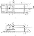
従来用いられている光モジュール(従来例1)を、図1(a)および図1(b)を用い説明する。図1(a)は従来例に係る光モジュールの上視図(キャップは図示していない)であり、図1(b)は図1(a)のA−A断面図である。パッケージ20は取付部となるフランジ26においてネジ27によりヒートシンク10用の基板に固定されている。ヒートシンク10は例えばCuまたはAlにより構成されている。パッケージ20は側壁22と底部24とからなり、底部24はフランジ26と一体化して形成されている。側壁22および底部24は例えばFe−Ni−Co合金であるコバール(商品名)により構成される。フランジ26は底部24の4つの角部に設けられている。側壁22の一面には開口部23が設けられ光ファイバ12がパッケージ20内に挿入されている。つまりパッケージ20はその側壁22に光ファイバ12が貫通している。光ファイバ12は第1固定部14により側壁22に固定されている。
A conventionally used optical module (conventional example 1) will be described with reference to FIGS. 1 (a) and 1 (b). FIG. 1A is a top view (a cap is not shown) of an optical module according to a conventional example, and FIG. 1B is a cross-sectional view taken along line AA of FIG. The
光ファイバ12の一端は固定部材40と光ファイバ支持部42とからなる第2固定部16によりパッケージ20内に固定されている。光ファイバ12の光軸上にはレンズホルダ34で支持されたレンズ32と、半導体レーザ30がサブマウント44に配設され、光ファイバ12と半導体レーザ30とは光結合している。固定部材40およびサブマウント44はベース46上に固定され、サブマウント44は温度を一定に保つためのサーモモジュール48上に固定されている。サーモモジュール48は底部24に固定されている。このようにして、光ファイバ12は第1固定部14および第2固定部16に固定されている。このとき、第1固定部14の光ファイバ12を固定する先端と第2固定部16の光ファイバ12を固定する先端の間隔をLとする。なお、図1(a)および図1(b)では、レンズホルダ34をサブマウント44に固定しているが、レンズホルダをベース46上に固定する場合もある。
One end of the
光モジュールは−40〜85℃の環境温度に曝されるため、ヒートシンク10、パッケージ20および光ファイバ12の線熱膨張係数の差により生じる応力(以下、熱応力)が光ファイバ12に加わる。特許文献1には、この熱応力により、光ファイバ12の断線や光ファイバ12の固定部からの脱落等の信頼性の低下が生じる可能性があることが開示されている。また、光ファイバ12の断線や光ファイバ12の第2固定部16がベース46から脱落するのを防止するため、光ファイバ12に予め撓みを設ける技術(従来例2)が開示されている。図2に従来例2に係る光モジュールの断面図を示す。図1(a)と同じ部材は同じ符号を付し説明を省略する。図2に示すように、第1固定部14と第2固定部16との間に撓みを持ち、このときの光ファイバ12の曲率半径をrとする。
従来例1に係る光モジュールは、前述の熱応力に起因した信頼性低下以外にも、熱応力に起因し、光ファイバ12と半導体レーザ30との相対位置が変位しその光結合率が低下する。これでは光モジュールの品質を保つことができない。一方、従来例2の方法を用い、信頼性や品質を確保しようとする場合、以下のような課題がある。光ファイバの曲率半径rは光学的あるいは機械的な制約から30mm以上とすることが求められている(30mmを限界曲率半径という)。このため、従来例2において、光モジュールの温度範囲である−40〜85℃において光ファイバ12の曲率半径を30mm以下に保つためには、第1固定部14と第2固定部16との間隔Lを長くすることが求められる。このように、光モジュールの信頼性や品質を確保しようとすると、光モジュールを小型化することが難しくなる。
In the optical module according to Conventional Example 1, the relative position between the
本発明は、上記課題に鑑みさなれたものであり、信頼性や品質を確保し、かつ小型化の可能な光モジュールを提供することを目的とする。 The present invention has been made in view of the above problems, and an object thereof is to provide an optical module that can ensure reliability and quality and can be miniaturized.
本発明は、側壁に光ファイバが貫通するパッケージと、前記光ファイバを前記パッケージの側壁に固定する部材からなる第1固定部と、前記光ファイバを前記パッケージ内で固定する部材からなる第2固定部と、前記パッケージの対角となる2つの角部または前記角部の近傍の前記パッケージの辺にそれぞれ設けられ、それぞれの取付部において先端からパッケージまでの前記取付部の幅が同じである2つのみの前記取付部と、を具備し、前記第1固定部と前記第2固定部との間隔は6mm以下であり、前記光ファイバの挿入方向に対し、前記2つのみの取付部を結ぶ線が斜めとなるように前記2つのみの取付部が設けられることを特徴とする光モジュールである。本発明によれば、光ファイバに加わる熱応力を緩和できるため、信頼性や品質を確保し、かつ小型化の可能な光モジュールを提供することができる。
The present invention provides a package in which an optical fiber passes through a side wall, a first fixing portion made of a member for fixing the optical fiber to the side wall of the package, and a second fixing made of a member for fixing the optical fiber in the package. And the two corners that are diagonal to the package or the sides of the package in the vicinity of the corners , and the width of the mounting part from the tip to the package is the same in each
本発明は、側壁に光ファイバが貫通するパッケージと、前記光ファイバを前記パッケージの側壁に固定する部材からなる第1固定部と、前記光ファイバを前記パッケージ内で固定する部材からなる第2固定部と、前記パッケージの底面の前記光ファイバの挿入方向に対し概平行で相対する2つの辺にそれぞれ設けられ、それぞれの取付部において先端からパッケージまでの前記取付部の幅が同じである2つのみの前記取付部と、を具備し、前記第1固定部と前記第2固定部との間隔は6mm以下であり、前記光ファイバの挿入方向に対し、前記2つのみの取付部を結ぶ線が斜めとなるように前記2つのみの取付部が設けられることを特徴とする光モジュールである。本発明によれば、光ファイバに加わる熱応力を緩和できるため、信頼性や品質を確保し、かつ小型化の可能な光モジュールを提供することができる。 The present invention provides a package in which an optical fiber passes through a side wall, a first fixing portion made of a member for fixing the optical fiber to the side wall of the package, and a second fixing made of a member for fixing the optical fiber in the package. and parts, respectively provided on two opposite sides in approximate parallel to the insertion direction of the optical fiber of the bottom surface of the package, two width of the mounting portion from the tip until the package is the same in each of the mounting portion comprising said attachment part only, a distance between the second fixing portion and the first fixing portion is Ri der below 6 mm, with respect to the insertion direction of the optical fiber, connecting the only two attachment portions The optical module is characterized in that only the two attachment portions are provided so that the line is inclined . According to the present invention, since thermal stress applied to an optical fiber can be relaxed, an optical module that can ensure reliability and quality and can be miniaturized can be provided.
本発明の前記2つの取付部は、前記パッケージの角部近傍の前記2つの辺に設けられ、前記2つの辺は、前記光ファイバの挿入方向に概平行で相対する辺であることを特徴とする光モジュールとすることができる。また、本発明の前記2つの取付部は、前記パッケージの角部近傍の前記2つの辺に設けられ、前記2つの辺は、前記光ファイバの挿入方向に概直角で相対する辺であることを特徴とする光モジュールとすることができる。 The two attachment portions of the present invention are provided on the two sides in the vicinity of the corner of the package, and the two sides are sides substantially parallel to and opposite to the insertion direction of the optical fiber. It can be set as an optical module. Further, the two attachment portions of the present invention are provided on the two sides in the vicinity of the corner of the package, and the two sides are sides opposite to each other at a substantially right angle with respect to the insertion direction of the optical fiber. It can be set as the optical module characterized.
本発明の前記2つの取付部は、前記光ファイバの挿入方向を対称軸に概相対する位置に設けられたことを特徴とする光モジュールとすることができる。本発明によれば、光ファイバに加わる熱応力を一層緩和できるため、信頼性や品質を一層確保し、かつ一層小型化の可能な光モジュールを提供することができる。 The two mounting portions of the present invention can be an optical module characterized in that the optical fiber insertion direction is provided at a position approximately opposite to the axis of symmetry. According to the present invention, since the thermal stress applied to the optical fiber can be further relaxed, it is possible to provide an optical module that can further ensure reliability and quality and can be further miniaturized.
本発明は、前記側壁に接続され、前記側壁と前記第1固定部との間に設けられ、温度変化によって、前記光ファイバの前記第1固定部と前記第2固定部の間に掛かる応力が小さくなるように、前記パッケージの底部より線熱膨張係数が大きい緩衝部材を具備し、前記第1固定部は、前記緩衝部材を介し前記側壁に固定されることを特徴とする光モジュールとすることができる。本発明によれば、緩衝部材により光ファイバに加わる応力を緩和することができるため、信頼性や品質を一層確保し、かつ一層小型化の可能な光モジュールを提供することができる。 The present invention is connected to the side wall, provided between the side wall and the first fixing portion, and stress applied between the first fixing portion and the second fixing portion of the optical fiber due to a temperature change. A buffer member having a linear thermal expansion coefficient larger than that of the bottom portion of the package is provided so as to be small , and the first fixing portion is fixed to the side wall via the buffer member. Can do. According to the present invention, since the stress applied to the optical fiber by the buffer member can be relaxed, it is possible to provide an optical module that can further ensure reliability and quality and can be further miniaturized.
本発明は、側壁に光ファイバが貫通するパッケージと、前記光ファイバに接続され、前記光ファイバを固定する部材からなる第1固定部と、前記光ファイバを前記パッケージ内で固定する部材からなる第2固定部と、前記側壁に接続され、前記側壁の内側と前記第1固定部との間に設けられた緩衝部材と、を具備し、前記光ファイバは、前記第1固定部および前記緩衝部材を介して、前記側壁に固定され、前記緩衝部材は、温度変化によって、前記光ファイバの前記第1固定部と前記第2固定部の間に掛かる応力が小さくなるように、前記パッケージの底部より線熱膨張係数が大きく、前記第1固定部と前記第2固定部との間隔は6mm以下であることを特徴とする光モジュールである。本発明によれば、緩衝部材により光ファイバに加わる応力を緩和することができるため、信頼性や品質を確保し、かつ小型化の可能な光モジュールを提供することができる。 The present invention includes a package which the optical fiber penetrates the side wall, is connected to the optical fiber, a first fixing part comprising a member for fixing the optical fiber, first consists member for fixing said optical fiber in said package Two fixing parts, and a buffer member connected to the side wall and provided between the inside of the side wall and the first fixing part, wherein the optical fiber includes the first fixing part and the buffer member The buffer member is fixed to the side wall via the bottom of the package so that the stress applied between the first fixing portion and the second fixing portion of the optical fiber is reduced due to a temperature change. The optical module has a large linear thermal expansion coefficient, and an interval between the first fixing portion and the second fixing portion is 6 mm or less. According to the present invention, since the stress applied to the optical fiber by the buffer member can be relaxed, it is possible to provide an optical module that can ensure reliability and quality and can be miniaturized.
本発明の前記緩衝部材は、前記側壁を貫通して前記側壁に接続されてなることを特徴とする光モジュールとすることができる。また、本発明は、前記パッケージ内に前記光ファイバと光結合する光半導体素子を具備する光モジュールとすることができる。 The buffer member according to the present invention may be an optical module that is connected to the side wall through the side wall. In addition, the present invention can be an optical module including an optical semiconductor element optically coupled to the optical fiber in the package.
本発明の前記パッケージは、取付部を有し、前記取付部により、前記パッケージの底面を形成する前記パッケージの底部より線熱膨張係数の大きい基板上に取り付けられることを特徴とする光モジュールとすることができる。本発明によれば、パッケージの底部より線熱膨張係数が大きく光ファイバに熱応力が加わり易い基板にパッケージを取り付けた光モジュールにおいても、信頼性や品質を確保し、かつ小型化の可能な光モジュールを提供することができる。 The package of the present invention has an attachment portion, and is attached to a substrate having a larger linear thermal expansion coefficient than the bottom portion of the package forming the bottom surface of the package by the attachment portion. be able to. According to the present invention, even in an optical module in which a package is mounted on a substrate having a linear thermal expansion coefficient larger than that of the bottom of the package and in which thermal stress is likely to be applied to an optical fiber, reliability and quality can be ensured and miniaturization is possible. Modules can be provided.
本発明によれば、信頼性や品質を確保し、かつ小型化の可能な光モジュールを提供することができる。 ADVANTAGE OF THE INVENTION According to this invention, reliability and quality can be ensured and the optical module which can be reduced in size can be provided.
以下、図面を参照し、本発明に係る実施例につき説明する。 Embodiments according to the present invention will be described below with reference to the drawings.
実施例1に係る光モジュールはヒートシンクにパッケージを取り付けるためのフランジをパッケージの底部の対角の位置に設けた例である。図3(a)は実施例1に係る光モジュールの上視図(キャップは図示していない)、図3(b)は図3(a)のB−B断面図、図3(c)はパッケージ20の底部24並びにフランジ26aおよび26bの平面図である。実施例1は従来例1に比較し、パッケージ20の底面の対角となる2つの角部にそれぞれ2つのフランジ26aおよび26bが設けられている。その他の構成は実施例1と同じであり、同じ部材は同じ符号を付し説明を省略する。図3(c)に示すように、パッケージ20の底部24とフランジ26a、26bは一体に形成されている。パッケージ20の底面は、4つの辺L1からL4と4つの角部T1からT4を有している。ここで、角部T1からT4は辺と辺の間の曲部を示している。2つのフランジ26aおよび26bはパッケージの底面の対角となる角部T3およびT1に設けられており、フランジ26aおよび26bは光ファイバ12の挿入方向に概平行方向に配置されている。
The optical module according to Example 1 is an example in which flanges for attaching a package to a heat sink are provided at diagonal positions on the bottom of the package. 3A is a top view of the optical module according to the first embodiment (a cap is not shown), FIG. 3B is a cross-sectional view taken along line BB in FIG. 3A, and FIG. It is a top view of
次いで、実施例1に係る光モジュールの製造方法について説明する。まず、半導体レーザ30と、レンズ32を収めたレンズホルダ34をサブマウント44に固定する。次に、サブマウント44をベース46に固定する。パッケージ20の底部24に固定されたサーモモジュール48上にベース46を固定する。固定部材40をベース上に配置する。光ファイバ12にフェルールである光ファイバ支持部42を固定し、光ファイバ12の先端をパッケージ20の側壁22に設けられた開口部23より挿入し、固定部材40に挿入する。光ファイバ12と半導体レーザ30が所望の光結合が得られるように、固定部材40、光ファイバ支持部42および光ファイバ12を配置して固定する。これにより、光ファイバ12は第2固定部に固定される。光ファイバ12をガラス等からなる第1固定部により側壁22に固定する。パッケージ20上にキャップ(図示せず)を設け気密封止する。なお、光ファイバ12をパッケージ20の側壁22の開口部23に固定することが可能であれば、半田等を用いても良い。その後、実施例1に係る光モジュールをフランジ26aおよび26bを用いヒートシンク10に取り付ける。
Next, a method for manufacturing the optical module according to Example 1 will be described. First, the
ここで、サブマウント44、ベース46、固定部材40、光ファイバ支持部42は例えばコバール等の金属、セラミックから構成され、その固定には例えば接着剤、半田またはYAG溶接が用いられる。第2固定部16での光ファイバ12の固定には例えば接着剤または半田等が用いられる。
Here, the
実施例1に係る光モジュールにより、信頼性や品質を確保できる理由について説明する。光ファイバ12の線熱膨張係数は0.55μ/℃に対し、一般的にパッケージ20の側壁22および底部24に用いられる材料であるコバール、Al2O3(アルミナ)、CuW等の線熱膨張係数は約8μ/℃、ヒートシンク10に用いられる材料であるAl、Cu等の線熱膨張係数は約20μ/℃である。このように、ヒートシンク10とパッケージ20と光ファイバ12との線熱膨張係数は大きく異なる。実施例1に係る光モジュールは、パッケージ20の底面を形成するパッケージ20の底部24より線熱膨張係数が大きいヒートシンク10に、2つのフランジ26aおよび26bによりパッケージ20が取り付けられている。例えば、光モジュールの温度が高くなった場合、従来例1に係る光モジュールでは、パッケージ20の底部24の4つの角部がフランジ26によりヒートシンク10に固定されているため、ヒートシンク10とパッケージ20の線熱膨張係数の差により、パッケージ20の4つの角部のフランジ等に熱応力が加わる。このため、パッケージ20はパッケージ20の本来の線熱膨張係数以上に伸長する。光ファイバ12の線熱膨張係数はヒートシンク10、パッケージ20に比べ非常に小さいため、光ファイバ12は挿入方向に伸長しようとする熱応力が加わる。
The reason why reliability and quality can be ensured by the optical module according to the first embodiment will be described. The linear thermal expansion coefficient of the
一方、実施例1に係る光モジュールは、光モジュールの温度が高くなった場合、パッケージ20の底部24のフランジ26が設けられ、ヒートシンク10に固定されている対角の2つの角部T1、T3に力が加わる。他の2つの角部T2、T4は固定されていないため、パッケージ20は対角の角部T1とT3との方向に伸長する。このため、辺L4の中心付近の光ファイバ12には斜め方向すなわち光ファイバの挿入方向とは非平行な方向に熱応力が加わる。このように、従来例1では光ファイバ12に対し主に挿入方向の熱応力が加わるのに対し、実施例1では光ファイバ12に斜め方向の熱応力が加わる。そのため、実施例1では光ファイバ12の挿入方向に加わる熱応力を従来例1より小さくすることができる。光モジュールの温度が低くなった場合も同様に光ファイバ12の挿入方向に加わる熱応力を小さくすることができる。光ファイバ12の断線や光ファイバ12の固定部からの脱落等の信頼性低下、光ファイバ12と半導体レーザ30との光結合率の低下等による品質の低下は、光ファイバ12の挿入方向に加わる熱応力に起因するため、実施例1においては、光ファイバ12の挿入方向に加わる熱応力を小さくすることにより、熱応力に起因した信頼性や品質の低下を抑制し、信頼性や品質の確保が可能となる。
On the other hand, in the optical module according to the first embodiment, when the temperature of the optical module increases, the
次に、従来例2のように光ファイバ12に撓みを持たせた場合の第1固定部14と第2固定部16との間隔Lの制限について検討する。光モジュールの曝される環境温度の最高温度Tmax=85℃で、光ファイバ12の撓みがない状態とする。このとき、光ファイバ12の熱膨張係数はヒートシンク10、パッケージ20の材料に比べ無視できるほど小さいため、光ファイバ12のTmaxからTminの間での温度依存による長さの変化はないと仮定する。この状態で最低温度のTmin=−40℃まで温度を変化させたとき、光ファイバ12に生じる撓みの曲率半径rとLの関係は次式となる。
2×(2πr)×sin−1(L/2r)/360°=
L×(α×(Tmax−Tmin)+1)
αはヒートシンク10の線熱膨張係数である。
Next, the limitation on the distance L between the first fixing
2 × (2πr) × sin −1 (L / 2r) / 360 ° =
L × (α × (Tmax−Tmin) +1)
α is a linear thermal expansion coefficient of the
パッケージをどのような材料で構成されたヒートシンク10に取り付けるかは任意に決められるが、ヒートシンクとして一般的に用いられる材料の中で最も線熱膨張係数の大きいAlを想定しておくことが好ましい。よって、ヒートシンク10として一般的に使用される材料の中で、線熱膨張係数αの最も大きいAl(α=23.6μ/℃)の値を用いた場合について検討する。この場合、光ファイバ12の撓みの曲率半径rが前述の限界曲率半径である30mm以上とするためには、Lは8mm以上が必要となる。つまり、光モジュールの温度−40〜85℃で光ファイバ12の撓みによる光ファイバ12の曲率半径rを30mmより大きく保つためには、Lを8mm以上とすることが求められる。さらに、製造の余裕を考慮すると10mm以上が求められる。
Although what kind of material is used to attach the package to the
このように、Lの下限が決められると、光モジュールの小型化の妨げとなる。また、光ファイバ12に撓みを設けることは製造上高度な管理を必要とする。つまり、熱応力に対し十分な撓みを持たせることと、制限曲率半径を越えないことの両方を満足するように、製造することが求められる。これには、各種製造装置あるいは冶具を利用した自動化困難な組み立て作業が求められる。
Thus, if the lower limit of L is determined, it will hinder downsizing of the optical module. Further, providing the
実施例1によれば、光ファイバ12に加わる挿入方向の熱応力を小さくできるため、第1固定部14と第2固定部16との間隔Lが10mm以下であっても、信頼性や品質を確保することができる。従来は、Lが6mm以下では光ファイバ12に撓みを設けることは困難であったが、実施例1によれば、Lが6mm以下であっても、信頼性や品質を確保し、かつ小型化の可能な光モジュールを提供することができる。また、光ファイバ12に撓みを持たせる場合も従来例2のように、製造上の高度な管理を要しない。なお、Lは5mm以下が好ましく、より好ましくは4mm以下である。
According to the first embodiment, the thermal stress in the insertion direction applied to the
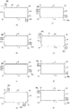
図4(a)から図4(g)は実施例1の各種変形例のパッケージ20の底部24並びにフランジ26aおよび26bを示す図である。図3(c)と同じ部材は同じ符号を付す。図4(a)は、光ファイバ12の挿入方向に対し概直角方向にフランジ26aおよび26bが角部T1およびT3に設けられる。
4 (a) to 4 (g) are diagrams showing the bottom 24 and the
図4(b)は、フランジ26aおよび26bが、パッケージ20の底面の対角となる2つの角部T1およびT3に接し、かつパッケージ20の角部T1およびT3の近傍の底面の光ファイバ12の挿入方向に概直角で相対する2つの辺に設けられている。
4B, the
図4(c)は、フランジ26aおよび26bが、パッケージ20の底面の対角となる2つの角部T1およびT3の近傍のパッケージ20の底面の2つの辺で、光ファイバ12の挿入方向に概直角で相対する2つの辺に設けられている。
FIG. 4 (c) shows that the
図4(d)は、フランジ26aおよび26bが、パッケージ20の底面の対角となる2つの角部T1およびT3に近傍で、光ファイバ12の挿入方向に概平行で相対するパッケージ20の底面の2つの辺に設けられている。
4D shows that the
図4(e)は、フランジ26aは角部T3に、フランジ26bは角部T1の近傍の辺L2に設けられている。
In FIG. 4E, the
図4(f)は、フランジ26aおよび26bが角部T1およびT3に設けられており、フランジ26aおよび26bは光ファイバ12の挿入方向とは非平行に配置されている。
In FIG. 4 (f),
図4(g)および図4(h)は、角部T1からT4がパッケージ20の底面を形成する長方形の頂点となっている例である。図4(g)は、フランジ26aおよび26bがパッケージ20の底面の対角となる2つの角部T1およびT3に接し、かつ光ファイバ12の挿入方向に概直角で相対するパッケージ20の底面の2つの辺に設けられている。
FIG. 4G and FIG. 4H are examples in which corner portions T1 to T4 are the vertices of a rectangle that forms the bottom surface of the
図4(h)は、フランジ26aおよび26bが、パッケージ20の底面の対角となる2つの角部T1およびT3に設けられ、かつ光ファイバ12の挿入方向に概直角で相対するパッケージ20の底面の2つの辺に設けられている。
FIG. 4H shows the bottom surface of the
以上示した変形例において、光ファイバ12に加わる熱応力は、光ファイバ12に斜め方向に加わる。したがって、光ファイバ12の挿入方向の熱応力を従来例1に比べ小さくできるため、光モジュールの信頼性や品質を確保し、小型化が可能となる。なお、フランジ26a、26bが角部T3、T1の近傍の辺L4、L2に設けられている場合は、フランジ26a、26bは辺L4、L2の中心点より、それぞれ角部T3、T1側にあればよい。これにより、光ファイバ12には、斜め方向に熱応力が加わり、光ファイバ12の挿入方向の熱応力を従来例1に対し小さくすることができる。よりその効果を十分発揮するためには、フランジ26aおよび26bは、角部T3、T1に近いことが好ましい。なお、実施例1ではフランジ26aおよび26bを角部T3、T1またはその近傍に設ける場合について例示したが、フランジ26aおよび26bは角部T4、T2またはその近傍に設けても良い。
In the modification shown above, the thermal stress applied to the
実施例2に係る光モジュールは、パッケージをヒートシンクに取り付けるフランジをパッケージの底部の光ファイバの挿入方向に対して概平行で相対する辺に設けた例である。実施例2を示す図5は、フランジ26aおよび26bの取り付け位置以外は実施例1と同じであり説明を省略する。図5(a)から図5(c)は実施例2およびその変形例のパッケージ20の底部24並びにフランジ26aおよび26bを示す図である。図5(a)は、フランジ26aおよび26bが、パッケージ20の底面の光ファイバ12の挿入方向に対し概平行に相対する2つの辺L3およびL1の中心位置にそれぞれ設けられている。
The optical module according to the second embodiment is an example in which a flange for attaching a package to a heat sink is provided on a side that is substantially parallel to and opposite to the optical fiber insertion direction at the bottom of the package. FIG. 5 showing the second embodiment is the same as the first embodiment except for the attachment positions of the
図5(b)は、フランジ26aおよび26bが、パッケージ20の底面の光ファイバ12の挿入方向に対し概平行に相対する2つの辺L3およびL1にあり、フランジ26aは辺L3の中心位置、フランジ26bは角部T4に接して、設けられている。
In FIG. 5B, the
図5(c)は、フランジ26aおよび26bが、パッケージ20の底面の光ファイバ12の挿入方向に対し概平行に相対する2つの辺L3およびL1にあり、光ファイバ12の挿入方向を対称軸に概相対する位置に設けられている。
FIG. 5 (c) shows that the
実施例2においては、パッケージ20は辺L1およびL3に設けられたフランジ26aおよび26bでヒートシンク10に固定されている。光モジュールの温度が高くなった場合、光ファイバ12の挿入方向と概直角方向に力が加わる。このため、パッケージ20には光ファイバ12の挿入方向と概直角方向に伸長しようとするため、光ファイバ12の挿入方向に加わる熱応力は小さい。したがって、実施例1と同様に、信頼性や品質を確保し、かつ小型化の可能な光モジュールを提供することができる。
In the second embodiment, the
特に、図5(a)および図5(c)のように、フランジ26aおよび26bを、辺L3およびL1の光ファイバ12の挿入方向を対称軸に概相対する位置に設けることにより、光ファイバ12はその挿入方向にほとんど熱応力が加わらない。よって、信頼性や品質を一層確保し、かつ一層小型化の可能な光モジュールを提供することができる。
In particular, as shown in FIGS. 5 (a) and 5 (c), the
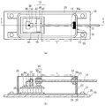
実施例3は側壁と第1固定部との間に緩衝部材を設けた例である。図6(a)は実施例3に係る光モジュールの上視図(キャップは図示していない)、図6(b)は図6(a)のC−C断面図である。従来例1の図1(a)および図1(b)に対し側壁22と第1固定部14との間に緩衝部材18aが設けられている。また、レンズ32を収めたレンズホルダ33は、直接ベース46に固定している。なお、レンズホルダ33は実施例1と同様にサブマウント44に配設されても良い。その他の構成は実施例1と同じであり、同じ部材は同じ符号を付し説明を省略する。図6(a)および図6(b)に示すように、緩衝部材18aは側壁22の内側に突出して、側壁22の内側と第1固定部14との間に設けられ、側壁22に固定されている。第1固定部14は側壁22と第2固定部16との間にあり、緩衝部材18aを介して側壁22に固定されている。つまり、緩衝部材18aは、側壁22に接続され、側壁22と第2固定部16との間に延在している。光ファイバ12は、緩衝部材18aと第1固定部14を介して側壁22に固定されている。緩衝部材18aはパッケージ20の側壁22内側に突出しており、突出している部分が温度変化により膨張または収縮することで光ファイバにかかる熱応力が小さくなる。
Example 3 is an example in which a buffer member is provided between the side wall and the first fixing portion. 6A is a top view of the optical module according to the third embodiment (a cap is not shown), and FIG. 6B is a cross-sectional view taken along the line CC in FIG. 6A. A
緩衝部材18aとしては、パッケージ20の底部24の材料より線熱膨張係数の大きな材料が好ましく、例えばCr−Ni−Fe系合金のSUS304、Cr−Ni系合金のSUS430等を用いる。例えば光モジュールの温度が上昇した場合、パッケージ20の側壁22および底部24は膨張し側壁22と第2固定部16との間隔は広くなる。しかし、第1固定部14と側壁22との間の緩衝部材18aも膨張するため、第1固定部14と第2固定部16との間隔の伸長は、パッケージ20による伸長と緩衝部材18aによる伸長との差となり、従来例1に比べ、光ファイバ12に加わる熱応力を小さくすることができる。
As the
また、緩衝部材18aの線熱膨張係数を、パッケージ20の底部22の線熱膨張係数より大きくすることにより、光ファイバ12に加わる熱応力をより小さくすることができる。
Further, by making the linear thermal expansion coefficient of the
さらに、実施例1のように、第1固定部14と第2固定部16との間隔Lを6mm以下とすることにより、信頼性や品質を確保し、小型化の可能な光モジュールを提供することができる。
Further, as in the first embodiment, the distance L between the first fixing
図7は実施例4に係る光モジュールの上視図(キャップを図示せず、開口部23を透視し細線で図示した)である。実施例4は実施例3に比較し、緩衝部材18bは光ファイバ12が貫通するための側壁22の開口部23を通り側壁22の内側および外側に設けられている。その他の構成は実施例3と同じであり、同じ部材は同じ符号を付し説明を省略する。このように、緩衝部材18bは側壁22を貫通して側壁22に接続することにより、簡単に緩衝部材18bを配置することができる。
FIG. 7 is a top view of the optical module according to the fourth embodiment (a cap is not shown, the
図8は実施例5に係る光モジュールの上視図(キャップを図示せず、開口部23を透視し細線で図示した)である。実施例5は実施例4に比較し、フランジ26aおよび26bが実施例1と同様に設けられている。その他の構成は実施例4と同じであり、同じ部材は同じ符号を付し説明を省略する。このように、実施例3および実施例4のように緩衝部材18a、18bを設け、実施例1、実施例2およびこれらの変形例のようにフランジ26aおよび26bを設けることもできる。これにより、光ファイバ12に加わる熱応力を一層小さくすることができ、信頼性や品質を一層確保し、かつ一層小型化の可能な光モジュールを提供することができる。
FIG. 8 is a top view of the optical module according to the fifth embodiment (a cap is not shown, the
実施例3から実施例5においても、実施例1と同様に、パッケージ20の底部24より線熱膨張係数の大きい材料をヒートシンク10に用いている。つまり、パッケージ20は、フランジ26aおよび26bを有し、フランジ26aおよび26bによりパッケージ20の底面を形成するパッケージ20の底部24より線熱膨張係数の大きいヒートシンク10上に取り付けられている。
In the third to fifth embodiments, as in the first embodiment, a material having a larger linear thermal expansion coefficient than the bottom 24 of the
図9は実施例6に係る光モジュールの断面図である。実施例6は実施例1に比較し、第1固定部14が光ファイバ12をフェルール等の間接部材15を介し間接的にパッケージ20に固定している。実施例1から実施例5では、第2固定部16の間接部材として光ファイバ支持部42を用いていたが、これらの間接部材は金属、セラミック、樹脂等の部材を用いても良い。その他の構成は実施例1と同じであり、同じ部材は同じ符号を付し説明を省略する。実施例1から5並びにその変形例では、第1固定部14および第2固定部16は、光ファイバ12を直接的にパッケージ20に固定しても良いし、第1固定部14および第2固定部16の少なくとも一方が、間接部材15、光ファイバ支持部42を介し間接的にパッケージ20に固定しても良い。なお、光ファイバ12が間接部材15、光ファイバ支持部42を介し間接的に固定された場合、第1固定部14と第2固定部16との間隔Lは、図9に示すように、第1固定部14の先端と第2固定部16の先端との間で、間接部材15、光ファイバ支持部42により間接的に固定されていない間隔となる。
FIG. 9 is a cross-sectional view of an optical module according to the sixth embodiment. In the sixth embodiment, the first fixing
実施例1から実施例6並びにその変形例は、半導体レーザ30を光ファイバ12と光結合する例であったが、受光素子、発光ダイオード等の光半導体素子であってもよい。すなわち、光モジュールはパッケージ内に光ファイバと光結合する半導体素子を有していればよい。
Although the first to sixth embodiments and the modifications thereof are examples in which the
また、実施例1から実施例6並びにその変形例は、フランジ26aおよび26bがパッケージ20の底部24と一体化している例であったが、フランジ26aおよび26bがパッケージ20の底部24とは別の部材であってもよい。
In the first to sixth embodiments and the modifications thereof, the
以上、発明の好ましい実施形態について詳述したが、本発明は係る特定の実施形態に限定されるものではなく、特許請求の範囲に記載された本発明の要旨の範囲内において、種々の変形・変更が可能である。 The preferred embodiments of the present invention have been described in detail above. However, the present invention is not limited to the specific embodiments, and various modifications and changes can be made within the scope of the gist of the present invention described in the claims. It can be changed.
10 ヒートシンク
12 光ファイバ
14 第1固定部
15 間接部材
16 第2固定部
20 パッケージ
22 側壁
24 底部
26、26a、26b フランジ
27 ネジ
30 半導体レーザ
32 レンズ
L1、L2、L3、L4 辺
T1、T2、T3、T4 角部
DESCRIPTION OF
Claims (10)
前記光ファイバを前記パッケージの側壁に固定する部材からなる第1固定部と、
前記光ファイバを前記パッケージ内で固定する部材からなる第2固定部と、
前記パッケージの対角となる2つの角部または前記角部の近傍の前記パッケージの辺にそれぞれ設けられ、それぞれの取付部において先端からパッケージまでの前記取付部の幅が同じである2つのみの前記取付部と、を具備し、
前記第1固定部と前記第2固定部との間隔は6mm以下であり、
前記光ファイバの挿入方向に対し、前記2つのみの取付部を結ぶ線が斜めとなるように前記2つのみの取付部が設けられることを特徴とする光モジュール。 A package through which an optical fiber penetrates the side wall;
A first fixing part comprising a member for fixing the optical fiber to the side wall of the package;
A second fixing part made of a member for fixing the optical fiber in the package;
The two corners that are diagonal to the package or the sides of the package in the vicinity of the corners, respectively, and in each of the attachment parts, the width of the attachment part from the tip to the package is the same. The mounting portion,
Distance between the second fixing portion and the first fixing portion is Ri der below 6 mm,
The optical module is characterized in that only the two attachment portions are provided so that a line connecting only the two attachment portions is inclined with respect to the insertion direction of the optical fiber .
前記光ファイバを前記パッケージの側壁に固定する部材からなる第1固定部と、
前記光ファイバを前記パッケージ内で固定する部材からなる第2固定部と、
前記パッケージの底面の前記光ファイバの挿入方向に対し概平行で相対する2つの辺にそれぞれ設けられ、それぞれの取付部において先端からパッケージまでの前記取付部の幅が同じである2つのみの前記取付部と、を具備し、
前記第1固定部と前記第2固定部との間隔は6mm以下であり、
前記光ファイバの挿入方向に対し、前記2つのみの取付部を結ぶ線が斜めとなるように前記2つのみの取付部が設けられることを特徴とする光モジュール。 A package through which an optical fiber penetrates the side wall;
A first fixing part comprising a member for fixing the optical fiber to the side wall of the package;
A second fixing part made of a member for fixing the optical fiber in the package;
The approximate relative insertion direction of the optical fiber of the bottom surface of the package parallel with respectively provided on two opposite sides, the only two width of the mounting portion from the tip until the package is the same in each of the mounting portion An attachment portion,
Distance between the second fixing portion and the first fixing portion is Ri der below 6 mm,
The optical module is characterized in that only the two attachment portions are provided so that a line connecting only the two attachment portions is inclined with respect to the insertion direction of the optical fiber .
前記第1固定部は、前記緩衝部材を介し前記側壁に固定されることを特徴とする請求項1から5のいずれか一項記載の光モジュール。 Connected to the side wall, provided between the side wall and the first fixing portion, so that a stress applied between the first fixing portion and the second fixing portion of the optical fiber is reduced by a temperature change. A cushioning member having a larger coefficient of linear thermal expansion than the bottom of the package,
The optical module according to claim 1, wherein the first fixing portion is fixed to the side wall via the buffer member.
前記光ファイバに接続され、前記光ファイバを固定する部材からなる第1固定部と、
前記光ファイバを前記パッケージ内で固定する部材からなる第2固定部と、
前記側壁に接続され、前記側壁の内側と前記第1固定部との間に設けられた緩衝部材と、を具備し、
前記光ファイバは、前記第1固定部および前記緩衝部材を介して、前記側壁に固定され、
前記緩衝部材は、温度変化によって、前記光ファイバの前記第1固定部と前記第2固定部の間に掛かる応力が小さくなるように、前記パッケージの底部より線熱膨張係数が大きく、
前記第1固定部と前記第2固定部との間隔は6mm以下であることを特徴とする光モジュール。 A package through which an optical fiber penetrates the side wall;
A first fixing portion connected to the optical fiber and made of a member for fixing the optical fiber;
A second fixing part made of a member for fixing the optical fiber in the package;
A buffer member connected to the side wall and provided between the inner side of the side wall and the first fixing portion;
The optical fiber is fixed to the side wall via the first fixing portion and the buffer member,
The buffer member has a larger coefficient of linear thermal expansion than the bottom of the package so that a stress applied between the first fixing portion and the second fixing portion of the optical fiber is reduced due to a temperature change.
The optical module is characterized in that an interval between the first fixing portion and the second fixing portion is 6 mm or less.
Priority Applications (4)
| Application Number | Priority Date | Filing Date | Title |
|---|---|---|---|
| JP2005288895A JP4615414B2 (en) | 2005-09-30 | 2005-09-30 | Optical module |
| US11/520,714 US7393146B2 (en) | 2005-09-30 | 2006-09-14 | Optical module |
| CNB2006101599805A CN100460906C (en) | 2005-09-30 | 2006-09-29 | Optical module |
| CN2008101452528A CN101339279B (en) | 2005-09-30 | 2006-09-29 | Optical module |
Applications Claiming Priority (1)
| Application Number | Priority Date | Filing Date | Title |
|---|---|---|---|
| JP2005288895A JP4615414B2 (en) | 2005-09-30 | 2005-09-30 | Optical module |
Publications (3)
| Publication Number | Publication Date |
|---|---|
| JP2007101700A JP2007101700A (en) | 2007-04-19 |
| JP2007101700A5 JP2007101700A5 (en) | 2008-07-10 |
| JP4615414B2 true JP4615414B2 (en) | 2011-01-19 |
Family
ID=37902040
Family Applications (1)
| Application Number | Title | Priority Date | Filing Date |
|---|---|---|---|
| JP2005288895A Expired - Fee Related JP4615414B2 (en) | 2005-09-30 | 2005-09-30 | Optical module |
Country Status (3)
| Country | Link |
|---|---|
| US (1) | US7393146B2 (en) |
| JP (1) | JP4615414B2 (en) |
| CN (2) | CN101339279B (en) |
Families Citing this family (9)
| Publication number | Priority date | Publication date | Assignee | Title |
|---|---|---|---|---|
| JP2010109132A (en) * | 2008-10-30 | 2010-05-13 | Yamaha Corp | Thermoelectric module package and method of manufacturing the same |
| JP5693888B2 (en) | 2010-07-28 | 2015-04-01 | 住友電工デバイス・イノベーション株式会社 | Optical device and manufacturing method thereof |
| EP2698656A4 (en) * | 2011-04-13 | 2014-08-27 | Fujikura Ltd | Manufacturing method for optical module |
| CN203191077U (en) * | 2013-04-08 | 2013-09-11 | 宁波源禄光电有限公司 | Small temperature-stabilized spectrograph |
| JP6400316B2 (en) * | 2014-03-27 | 2018-10-03 | 住友電工デバイス・イノベーション株式会社 | Optical device |
| DE102016102327B4 (en) * | 2016-02-10 | 2018-02-08 | Schott Ag | Housing for an electronic component and laser module |
| JP2019090967A (en) * | 2017-11-16 | 2019-06-13 | 日本電信電話株式会社 | Optical module |
| TWI678568B (en) * | 2018-08-21 | 2019-12-01 | 傳承光電股份有限公司 | Optical transceiver device |
| US20230188241A1 (en) * | 2021-12-15 | 2023-06-15 | Applied Optoelectronics, Inc. | Holder for mounting optical components and an optical subassembly implementing same |
Citations (8)
| Publication number | Priority date | Publication date | Assignee | Title |
|---|---|---|---|---|
| JPH07159656A (en) * | 1993-12-01 | 1995-06-23 | Fujitsu Ltd | Package for optical semiconductor module |
| JPH07202345A (en) * | 1993-12-28 | 1995-08-04 | Anritsu Corp | Semiconductor laser module |
| JP2001100066A (en) * | 1999-07-23 | 2001-04-13 | Furukawa Electric Co Ltd:The | Optical component and its manufacturing method |
| JP2001194561A (en) * | 2000-01-14 | 2001-07-19 | Mitsubishi Electric Corp | Laser diode module |
| JP2003158330A (en) * | 2001-11-21 | 2003-05-30 | Opnext Japan Inc | Semiconductor laser coupler |
| JP2004128291A (en) * | 2002-10-04 | 2004-04-22 | Hitachi Ltd | Semiconductor laser module and optical transmission receptacle |
| JP2004259771A (en) * | 2003-02-24 | 2004-09-16 | Kyocera Corp | Package for housing optical semiconductor element and optical semiconductor device |
| JP2004301873A (en) * | 2003-03-28 | 2004-10-28 | Mitsubishi Electric Corp | Optical semiconductor device module |
Family Cites Families (9)
| Publication number | Priority date | Publication date | Assignee | Title |
|---|---|---|---|---|
| JPS6410686A (en) * | 1987-07-03 | 1989-01-13 | Hitachi Ltd | Semiconductor laser module with electronic cooling element |
| FR2623297B1 (en) * | 1987-11-13 | 1991-09-27 | Cit Alcatel | COUPLING DEVICE BETWEEN AN OPTICAL FIBER AND AN OPTOELECTRONIC COMPONENT |
| DE3807491A1 (en) * | 1988-03-08 | 1989-09-21 | Schott Glaswerke | METHOD AND DEVICE FOR HERMETICALLY CARRYING OUT A LIGHT WAVE GUIDE |
| US4936646A (en) * | 1989-08-23 | 1990-06-26 | Tektronix, Inc. | Temperature-compliant tube for fiber optic components |
| US6435736B1 (en) | 1999-07-23 | 2002-08-20 | The Furukawa Electric Co., Ltd. | Optical device and method for manufacturing the same |
| JP2003133461A (en) * | 2001-10-29 | 2003-05-09 | Kyocera Corp | Package for containing optical semiconductor element |
| CN2550783Y (en) | 2001-11-15 | 2003-05-14 | 鸿富锦精密工业(深圳)有限公司 | Optical fibre fixer |
| JP2003344713A (en) * | 2002-05-29 | 2003-12-03 | Kyocera Corp | Optical element module and manufacturing method |
| JP4563107B2 (en) * | 2004-08-09 | 2010-10-13 | 住友大阪セメント株式会社 | Light modulation element module |
-
2005
- 2005-09-30 JP JP2005288895A patent/JP4615414B2/en not_active Expired - Fee Related
-
2006
- 2006-09-14 US US11/520,714 patent/US7393146B2/en not_active Expired - Fee Related
- 2006-09-29 CN CN2008101452528A patent/CN101339279B/en not_active Expired - Fee Related
- 2006-09-29 CN CNB2006101599805A patent/CN100460906C/en not_active Expired - Fee Related
Patent Citations (8)
| Publication number | Priority date | Publication date | Assignee | Title |
|---|---|---|---|---|
| JPH07159656A (en) * | 1993-12-01 | 1995-06-23 | Fujitsu Ltd | Package for optical semiconductor module |
| JPH07202345A (en) * | 1993-12-28 | 1995-08-04 | Anritsu Corp | Semiconductor laser module |
| JP2001100066A (en) * | 1999-07-23 | 2001-04-13 | Furukawa Electric Co Ltd:The | Optical component and its manufacturing method |
| JP2001194561A (en) * | 2000-01-14 | 2001-07-19 | Mitsubishi Electric Corp | Laser diode module |
| JP2003158330A (en) * | 2001-11-21 | 2003-05-30 | Opnext Japan Inc | Semiconductor laser coupler |
| JP2004128291A (en) * | 2002-10-04 | 2004-04-22 | Hitachi Ltd | Semiconductor laser module and optical transmission receptacle |
| JP2004259771A (en) * | 2003-02-24 | 2004-09-16 | Kyocera Corp | Package for housing optical semiconductor element and optical semiconductor device |
| JP2004301873A (en) * | 2003-03-28 | 2004-10-28 | Mitsubishi Electric Corp | Optical semiconductor device module |
Also Published As
| Publication number | Publication date |
|---|---|
| CN101339279A (en) | 2009-01-07 |
| US20070077013A1 (en) | 2007-04-05 |
| CN100460906C (en) | 2009-02-11 |
| CN1940609A (en) | 2007-04-04 |
| JP2007101700A (en) | 2007-04-19 |
| US7393146B2 (en) | 2008-07-01 |
| CN101339279B (en) | 2010-06-02 |
Similar Documents
| Publication | Publication Date | Title |
|---|---|---|
| JP4615414B2 (en) | Optical module | |
| JP3861864B2 (en) | Optical module | |
| US6720582B2 (en) | Semiconductor laser diode module | |
| US6220765B1 (en) | Hermetically sealed optical-semiconductor container and optical-semiconductor module | |
| US8000567B2 (en) | Optical semiconductor module | |
| JPH0980266A (en) | Semiconductor laser module | |
| JP4976005B2 (en) | Semiconductor laser module | |
| JPH10190141A (en) | Optical semiconductor module | |
| JP6753478B2 (en) | Optical module | |
| JP6602479B1 (en) | Optical module | |
| US6963593B2 (en) | Semiconductor laser module and optical transmitter | |
| JP2007208065A (en) | Optical module | |
| JP2013197256A (en) | Semiconductor laser module and manufacturing method therefor | |
| JP2010263070A (en) | Semiconductor laser module and manufacturing method thereof | |
| JP3925690B2 (en) | Semiconductor laser module | |
| JP7102860B2 (en) | Optical module | |
| JP5201892B2 (en) | Optical communication package | |
| JP4308049B2 (en) | Semiconductor element module | |
| JP2003338654A (en) | Semiconductor laser module | |
| JP2004253409A (en) | Optical semiconductor element accommodating package and optical semiconductor device | |
| JP2007095942A (en) | Joint structure | |
| JP2004294746A (en) | Optical semiconductor module | |
| JP2007322815A (en) | Optical semiconductor module | |
| JP2006186166A (en) | Semiconductor laser element, and optical disk system using same | |
| JPS63198389A (en) | Light-emitting device equipped with optical fiber and its assembly |
Legal Events
| Date | Code | Title | Description |
|---|---|---|---|
| A521 | Request for written amendment filed |
Free format text: JAPANESE INTERMEDIATE CODE: A523 Effective date: 20080527 |
|
| A621 | Written request for application examination |
Free format text: JAPANESE INTERMEDIATE CODE: A621 Effective date: 20080527 |
|
| A977 | Report on retrieval |
Free format text: JAPANESE INTERMEDIATE CODE: A971007 Effective date: 20100301 |
|
| A131 | Notification of reasons for refusal |
Free format text: JAPANESE INTERMEDIATE CODE: A131 Effective date: 20100316 |
|
| A521 | Request for written amendment filed |
Free format text: JAPANESE INTERMEDIATE CODE: A523 Effective date: 20100517 |
|
| A131 | Notification of reasons for refusal |
Free format text: JAPANESE INTERMEDIATE CODE: A131 Effective date: 20100720 |
|
| A521 | Request for written amendment filed |
Free format text: JAPANESE INTERMEDIATE CODE: A523 Effective date: 20100827 |
|
| TRDD | Decision of grant or rejection written | ||
| A01 | Written decision to grant a patent or to grant a registration (utility model) |
Free format text: JAPANESE INTERMEDIATE CODE: A01 Effective date: 20101019 |
|
| A01 | Written decision to grant a patent or to grant a registration (utility model) |
Free format text: JAPANESE INTERMEDIATE CODE: A01 |
|
| A61 | First payment of annual fees (during grant procedure) |
Free format text: JAPANESE INTERMEDIATE CODE: A61 Effective date: 20101020 |
|
| R150 | Certificate of patent or registration of utility model |
Free format text: JAPANESE INTERMEDIATE CODE: R150 |
|
| FPAY | Renewal fee payment (event date is renewal date of database) |
Free format text: PAYMENT UNTIL: 20131029 Year of fee payment: 3 |
|
| LAPS | Cancellation because of no payment of annual fees |