JP4615217B2 - Method for manufacturing a semiconductor power device having a voltage sustaining layer having a trapezoidal trench for forming a floating island - Google Patents
Method for manufacturing a semiconductor power device having a voltage sustaining layer having a trapezoidal trench for forming a floating island Download PDFInfo
- Publication number
- JP4615217B2 JP4615217B2 JP2003533321A JP2003533321A JP4615217B2 JP 4615217 B2 JP4615217 B2 JP 4615217B2 JP 2003533321 A JP2003533321 A JP 2003533321A JP 2003533321 A JP2003533321 A JP 2003533321A JP 4615217 B2 JP4615217 B2 JP 4615217B2
- Authority
- JP
- Japan
- Prior art keywords
- power device
- semiconductor power
- trench
- region
- manufacturing
- Prior art date
- Legal status (The legal status is an assumption and is not a legal conclusion. Google has not performed a legal analysis and makes no representation as to the accuracy of the status listed.)
- Expired - Fee Related
Links
- 239000004065 semiconductor Substances 0.000 title claims description 92
- 238000004519 manufacturing process Methods 0.000 title claims description 39
- 238000000034 method Methods 0.000 title claims description 32
- 210000000746 body region Anatomy 0.000 claims description 35
- VYPSYNLAJGMNEJ-UHFFFAOYSA-N Silicium dioxide Chemical compound O=[Si]=O VYPSYNLAJGMNEJ-UHFFFAOYSA-N 0.000 claims description 21
- 239000012535 impurity Substances 0.000 claims description 21
- 239000000758 substrate Substances 0.000 claims description 20
- 239000000463 material Substances 0.000 claims description 17
- 238000005530 etching Methods 0.000 claims description 13
- 235000012239 silicon dioxide Nutrition 0.000 claims description 10
- 239000000377 silicon dioxide Substances 0.000 claims description 10
- 239000003989 dielectric material Substances 0.000 claims description 9
- 238000012423 maintenance Methods 0.000 claims description 9
- 229910044991 metal oxide Inorganic materials 0.000 claims description 8
- 150000004706 metal oxides Chemical class 0.000 claims description 8
- 238000009792 diffusion process Methods 0.000 claims description 7
- 230000004888 barrier function Effects 0.000 claims description 6
- ZOXJGFHDIHLPTG-UHFFFAOYSA-N Boron Chemical group [B] ZOXJGFHDIHLPTG-UHFFFAOYSA-N 0.000 claims description 5
- 229910052796 boron Inorganic materials 0.000 claims description 5
- 238000000151 deposition Methods 0.000 claims description 5
- 229910052581 Si3N4 Inorganic materials 0.000 claims description 3
- 230000005669 field effect Effects 0.000 claims description 3
- HQVNEWCFYHHQES-UHFFFAOYSA-N silicon nitride Chemical compound N12[Si]34N5[Si]62N3[Si]51N64 HQVNEWCFYHHQES-UHFFFAOYSA-N 0.000 claims description 3
- 230000015572 biosynthetic process Effects 0.000 claims 1
- 230000003647 oxidation Effects 0.000 claims 1
- 238000007254 oxidation reaction Methods 0.000 claims 1
- XUIMIQQOPSSXEZ-UHFFFAOYSA-N Silicon Chemical compound [Si] XUIMIQQOPSSXEZ-UHFFFAOYSA-N 0.000 description 9
- 229910052710 silicon Inorganic materials 0.000 description 9
- 239000010703 silicon Substances 0.000 description 9
- 238000002513 implantation Methods 0.000 description 6
- 230000015556 catabolic process Effects 0.000 description 5
- 230000005684 electric field Effects 0.000 description 5
- 229910021420 polycrystalline silicon Inorganic materials 0.000 description 5
- KRHYYFGTRYWZRS-UHFFFAOYSA-N Fluorane Chemical compound F KRHYYFGTRYWZRS-UHFFFAOYSA-N 0.000 description 4
- 230000000873 masking effect Effects 0.000 description 4
- 229920005591 polysilicon Polymers 0.000 description 4
- 230000002411 adverse Effects 0.000 description 2
- 229910052785 arsenic Inorganic materials 0.000 description 2
- RQNWIZPPADIBDY-UHFFFAOYSA-N arsenic atom Chemical compound [As] RQNWIZPPADIBDY-UHFFFAOYSA-N 0.000 description 2
- 238000001312 dry etching Methods 0.000 description 2
- 238000001020 plasma etching Methods 0.000 description 2
- 230000005540 biological transmission Effects 0.000 description 1
- 238000007796 conventional method Methods 0.000 description 1
- 125000004122 cyclic group Chemical group 0.000 description 1
- 230000008021 deposition Effects 0.000 description 1
- 238000010586 diagram Methods 0.000 description 1
- 235000012489 doughnuts Nutrition 0.000 description 1
- 230000000694 effects Effects 0.000 description 1
- 229910052751 metal Inorganic materials 0.000 description 1
- 239000002184 metal Substances 0.000 description 1
- 238000012986 modification Methods 0.000 description 1
- 230000004048 modification Effects 0.000 description 1
- 238000000059 patterning Methods 0.000 description 1
- 229920002120 photoresistant polymer Polymers 0.000 description 1
- 238000012545 processing Methods 0.000 description 1
- 229910052814 silicon oxide Inorganic materials 0.000 description 1
- 239000000126 substance Substances 0.000 description 1
Images


Classifications
-
- H—ELECTRICITY
- H01—ELECTRIC ELEMENTS
- H01L—SEMICONDUCTOR DEVICES NOT COVERED BY CLASS H10
- H01L29/00—Semiconductor devices adapted for rectifying, amplifying, oscillating or switching, or capacitors or resistors with at least one potential-jump barrier or surface barrier, e.g. PN junction depletion layer or carrier concentration layer; Details of semiconductor bodies or of electrodes thereof ; Multistep manufacturing processes therefor
- H01L29/66—Types of semiconductor device ; Multistep manufacturing processes therefor
- H01L29/68—Types of semiconductor device ; Multistep manufacturing processes therefor controllable by only the electric current supplied, or only the electric potential applied, to an electrode which does not carry the current to be rectified, amplified or switched
- H01L29/76—Unipolar devices, e.g. field effect transistors
- H01L29/772—Field effect transistors
- H01L29/78—Field effect transistors with field effect produced by an insulated gate
- H01L29/7801—DMOS transistors, i.e. MISFETs with a channel accommodating body or base region adjoining a drain drift region
- H01L29/7802—Vertical DMOS transistors, i.e. VDMOS transistors
-
- H—ELECTRICITY
- H01—ELECTRIC ELEMENTS
- H01L—SEMICONDUCTOR DEVICES NOT COVERED BY CLASS H10
- H01L21/00—Processes or apparatus adapted for the manufacture or treatment of semiconductor or solid state devices or of parts thereof
- H01L21/02—Manufacture or treatment of semiconductor devices or of parts thereof
- H01L21/04—Manufacture or treatment of semiconductor devices or of parts thereof the devices having at least one potential-jump barrier or surface barrier, e.g. PN junction, depletion layer or carrier concentration layer
- H01L21/18—Manufacture or treatment of semiconductor devices or of parts thereof the devices having at least one potential-jump barrier or surface barrier, e.g. PN junction, depletion layer or carrier concentration layer the devices having semiconductor bodies comprising elements of Group IV of the Periodic System or AIIIBV compounds with or without impurities, e.g. doping materials
-
- H—ELECTRICITY
- H01—ELECTRIC ELEMENTS
- H01L—SEMICONDUCTOR DEVICES NOT COVERED BY CLASS H10
- H01L29/00—Semiconductor devices adapted for rectifying, amplifying, oscillating or switching, or capacitors or resistors with at least one potential-jump barrier or surface barrier, e.g. PN junction depletion layer or carrier concentration layer; Details of semiconductor bodies or of electrodes thereof ; Multistep manufacturing processes therefor
- H01L29/02—Semiconductor bodies ; Multistep manufacturing processes therefor
- H01L29/06—Semiconductor bodies ; Multistep manufacturing processes therefor characterised by their shape; characterised by the shapes, relative sizes, or dispositions of the semiconductor regions ; characterised by the concentration or distribution of impurities within semiconductor regions
- H01L29/0603—Semiconductor bodies ; Multistep manufacturing processes therefor characterised by their shape; characterised by the shapes, relative sizes, or dispositions of the semiconductor regions ; characterised by the concentration or distribution of impurities within semiconductor regions characterised by particular constructional design considerations, e.g. for preventing surface leakage, for controlling electric field concentration or for internal isolations regions
- H01L29/0607—Semiconductor bodies ; Multistep manufacturing processes therefor characterised by their shape; characterised by the shapes, relative sizes, or dispositions of the semiconductor regions ; characterised by the concentration or distribution of impurities within semiconductor regions characterised by particular constructional design considerations, e.g. for preventing surface leakage, for controlling electric field concentration or for internal isolations regions for preventing surface leakage or controlling electric field concentration
- H01L29/0611—Semiconductor bodies ; Multistep manufacturing processes therefor characterised by their shape; characterised by the shapes, relative sizes, or dispositions of the semiconductor regions ; characterised by the concentration or distribution of impurities within semiconductor regions characterised by particular constructional design considerations, e.g. for preventing surface leakage, for controlling electric field concentration or for internal isolations regions for preventing surface leakage or controlling electric field concentration for increasing or controlling the breakdown voltage of reverse biased devices
- H01L29/0615—Semiconductor bodies ; Multistep manufacturing processes therefor characterised by their shape; characterised by the shapes, relative sizes, or dispositions of the semiconductor regions ; characterised by the concentration or distribution of impurities within semiconductor regions characterised by particular constructional design considerations, e.g. for preventing surface leakage, for controlling electric field concentration or for internal isolations regions for preventing surface leakage or controlling electric field concentration for increasing or controlling the breakdown voltage of reverse biased devices by the doping profile or the shape or the arrangement of the PN junction, or with supplementary regions, e.g. junction termination extension [JTE]
- H01L29/063—Reduced surface field [RESURF] pn-junction structures
- H01L29/0634—Multiple reduced surface field (multi-RESURF) structures, e.g. double RESURF, charge compensation, cool, superjunction (SJ), 3D-RESURF, composite buffer (CB) structures
-
- H—ELECTRICITY
- H01—ELECTRIC ELEMENTS
- H01L—SEMICONDUCTOR DEVICES NOT COVERED BY CLASS H10
- H01L29/00—Semiconductor devices adapted for rectifying, amplifying, oscillating or switching, or capacitors or resistors with at least one potential-jump barrier or surface barrier, e.g. PN junction depletion layer or carrier concentration layer; Details of semiconductor bodies or of electrodes thereof ; Multistep manufacturing processes therefor
- H01L29/66—Types of semiconductor device ; Multistep manufacturing processes therefor
- H01L29/66007—Multistep manufacturing processes
- H01L29/66075—Multistep manufacturing processes of devices having semiconductor bodies comprising group 14 or group 13/15 materials
- H01L29/66227—Multistep manufacturing processes of devices having semiconductor bodies comprising group 14 or group 13/15 materials the devices being controllable only by the electric current supplied or the electric potential applied, to an electrode which does not carry the current to be rectified, amplified or switched, e.g. three-terminal devices
- H01L29/66409—Unipolar field-effect transistors
- H01L29/66477—Unipolar field-effect transistors with an insulated gate, i.e. MISFET
- H01L29/66674—DMOS transistors, i.e. MISFETs with a channel accommodating body or base region adjoining a drain drift region
- H01L29/66712—Vertical DMOS transistors, i.e. VDMOS transistors
Description
本出願は、2001年10月4日に米国特許商標庁に出願された、米国特許出願番号第09/970,972号「フローティングアイランド電圧維持層を有する半導体パワーデバイスの製造方法(Method for Fabricating a Power Semiconductor Device Having a Floating Island Voltage Sustaining Layer)」に関連する。 This application is filed with the United States Patent and Trademark Office on October 4, 2001, US patent application Ser. No. 09 / 970,972, “Method for Fabricating a Semiconductor Power Device Having Floating Island Voltage Sustaining Layer”. Power Semiconductor Device Having a Floating Island Voltage Sustaining Layer ”.
本発明は、半導体パワーデバイスに関し、詳しくは、逆の伝導性にドープされたフローティングアイランドを用いて電圧維持層(voltage sustaining layer)を形成した金属酸化膜半導体電界効果トランジスタ及びこの他の半導体パワーデバイスに関する。 The present invention relates to a semiconductor power device, and more particularly, a metal oxide semiconductor field effect transistor in which a voltage sustaining layer is formed using a floating island doped with reverse conductivity and other semiconductor power devices. About.
縦型の二重拡散金属酸化膜半導体(Double-diffused Metal Oxide Semiconductor:以下、DMOSという。)、V溝DMOS(V-groove DMOS)、トレンチMOS電界効果トランジスタ(Field Effect Transistor:以下、FETという。)、絶縁ゲートバイポーラトランジスタ(Insulated Gate Bipolar Transistor:以下、IGBTという。)並びにダイオード及びバイポーラトランジスタ等の半導体パワーデバイスは、自動車の電気系統、電源装置、モータ駆動装置及び他の電源制御装置等の用途に採用されている。このような半導体パワーデバイスは、オフ状態では高い耐電圧を維持し、オン状態では低いオン抵抗、すなわち高い電流密度における低い電圧降下を有する必要がある。 Vertical double-diffused metal oxide semiconductor (hereinafter referred to as DMOS), V-groove DMOS (V-groove DMOS), trench MOS field-effect transistor (hereinafter referred to as FET). ), Insulated Gate Bipolar Transistor (hereinafter referred to as IGBT) and semiconductor power devices such as diodes and bipolar transistors are used in automobile electrical systems, power supply devices, motor drive devices, and other power supply control devices. Has been adopted. Such a semiconductor power device must maintain a high withstand voltage in the off state and have a low on-resistance in the on state, that is , a low voltage drop at a high current density .
図1は、nチャネルパワーMOSFETの典型的な構造を示す図である。n+にドープされたシリコン基板102上に形成されたn−エピタキシャルシリコン層101は、半導体デバイス内の2つのMOSFETセルに対応するpボディ領域105a、106aと、n+ソース領域107、108とを備える。pボディ領域105a、106aは、更に深いpボディ領域105b、106bとを含んでいてもよい。n+ソース領域107、108とpボディ領域105a、106aを接続するために、ソース及びボディ電極112がエピタキシャル層101の表面の特定の部分に広がっている。両セル用のn型ドレインは、図1に示す上部の半導体表面に延びているn型エピタキシャル層101の部分で形成される。ドレイン電極は、n+にドープされたシリコン基板102の底部に設けられている。絶縁層と導電層、例えば酸化層とポリシリコン層からなる絶縁ゲート電極118は、チャネルが形成されるボディ上及びエピタキシャル層101のドレイン部分の上に設けられている。
FIG. 1 is a diagram showing a typical structure of an n-channel power MOSFET. An n −
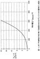
図1に示す従来のMOSFETのオン抵抗は、主にエピタキシャル層101のドリフト領域の抵抗(drift zone resistance)によって決定される。エピタキシャル層101は、n+にドープされたシリコン基板102とp+にドープされた深いボディ領域105b、106bとの間に印加される逆電圧に耐えなければならないので、電圧維持層(a voltage sustaining layer)と呼ばれることもある。一方、ドリフト領域の抵抗は、エピタキシャル層101のドープ濃度及び厚さによって決定される。なお、半導体デバイスの降伏電圧を高めるためには、エピタキシャル層101のドープ濃度を低くするとともに、エピタキシャル層101の厚さを増加させる必要がある。図2に示す曲線は、従来のMOSFETの単位面積当たりのオン抵抗を降伏電圧の関数として示している。この曲線から分かるように、降伏電圧を高くすると、半導体デバイスのオン抵抗は、急激に高くなってしまう。MOSFETを高い電圧、特に数百ボルト以上の電圧で動作させる場合、このオン抵抗の急激な上昇が問題となる。
The on-resistance of the conventional MOSFET shown in FIG. 1 is mainly determined by the drift zone resistance of the
図3は、高い電圧で動作するとともに、オン抵抗が低くなるように設計されたMOSFETを示している。このMOSFETは、セザック(Cezac)他著、ISPSD会報(Proceedings of the ISPSD)、2000年5月、69〜72頁、及びチェン(Chen)他著、電子機器に関するIEEEトランザクション第47−6(IEEE Transactions on Electron Devices Vol. 47, No. 6)、2000年6月、1280〜1285頁に開示されており、これらの文献の全体は、引用によって本願に援用されるものとする。このMOSFETは、電圧維持領域301のドリフト領域に縦方向に分離されて形成された一連のp+にドープされた層(所謂「フローティングアイランド(floating island)」)3101、3102、3103、・・・、310nを備えている点を除いて、図1に示す従来のMOSFETと略同じ構造を有している。フローティングアイランド3101、3102、3103、・・・、310nは、フローティングアイランドがない構造の場合よりも発生する電界は低い。発生する電界を低くすることにより、電圧維持領域301の一部を構成するエピタキシャル層において用いられる不純物濃度をより高くすることができる。フローティングアイランド3101、3102、3103、・・・、310nは、鋸歯状の電界プロファイルを生成し、これらの電界を積分することにより、従来の半導体デバイスで用いられていた不純物濃度より高い不純物濃度で、維持電圧を得ることができる。不純物濃度を高くすることにより、フローティングアイランドの層が全くない半導体デバイスに比べてオン抵抗が低い半導体デバイスを製造することができる。
FIG. 3 shows a MOSFET designed to operate at a high voltage and to have a low on-resistance. This MOSFET is disclosed in Cezac et al., Proceedings of the ISPSD, May 2000, pages 69-72, and Chen et al., IEEE Transactions 47-6 (IEEE Transactions on Electronic Equipment). on Electron Devices Vol. 47, No. 6), June 2000, pages 1280-1285, the entire contents of which are incorporated herein by reference. This MOSFET comprises a series of p + doped layers (so-called “floating islands”) 310 1 , 310 2 , 310 3 , formed vertically separated in the drift region of the
図3に示す構造は、複数回のエピタキシャル成長工程と、これに続く適切な不純物の導入を含む一連の処理によって形成される。ここで、エピタキシャル成長工程は、高価な工程であり、したがって、複数回のエピタキシャル成長工程を必要とする構造は、製造原価が高くなる。 The structure shown in FIG. 3 is formed by a series of processes including a plurality of epitaxial growth steps followed by introduction of appropriate impurities. Here, the epitaxial growth process is an expensive process. Therefore, a structure that requires a plurality of epitaxial growth processes has a high manufacturing cost.
そこで、図3に示すようなMOSFET構造を有する半導体パワーデバイスの製造方法であって、エピタキシャル成長工程の実施回数を減らし、より安価に半導体パワーデバイスを製造できる製造方法の実現が望まれている。 Therefore, it is desired to realize a manufacturing method of a semiconductor power device having a MOSFET structure as shown in FIG. 3, which can reduce the number of epitaxial growth steps and manufacture a semiconductor power device at a lower cost.
本発明は、半導体パワーデバイスの製造方法を提供する。この製造方法では、まず、第1の伝導型の基板を準備し、この基板上のエピタキシャル層内に電圧維持領域(voltage sustaining region)を形成する。この電圧維持領域の形成では、まず、基板上に、第1の伝導型を有するエピタキシャル層を成長させ、エピタキシャル層内に、2つ以上のトレンチを異なる深さにエッチングすることによって、少なくとも1つの雛壇状のトレンチ(terraced trench)を形成する。雛壇状のトレンチは、幅が異なる複数の部分を有し、各部分間に環状の棚を画定する。次に、雛壇状のトレンチの壁及び底部に沿ってバリア材を堆積させる。次に、環状の棚及びトレンチの底部に堆積されたバリア材を介して、エピタキシャル層の隣接する部分に、第2の伝導型の不純物を打ち込む。不純物を拡散させて、エピタキシャル層内に少なくとも1つの環状のドープ領域を形成する。更に、エピタキシャル層内の環状のドープ領域の下方に位置する少なくとも1つの他の領域を形成してもよい。続いて、雛壇状のトレンチ内に誘電体材料を堆積させて、雛壇状のトレンチを埋め込み、電圧維持領域が完成する。そして、電圧維持領域上に、第2の伝導型の領域を少なくとも1つ形成し、第2の導電型の領域と電圧維持領域との間に接合を画定する。 The present invention provides a method for manufacturing a semiconductor power device. In this manufacturing method, first, a substrate of a first conductivity type is prepared, and a voltage sustaining region is formed in an epitaxial layer on the substrate. In forming the voltage sustaining region, first, an epitaxial layer having a first conductivity type is grown on the substrate, and two or more trenches are etched in the epitaxial layer to different depths, thereby at least one of A terraced trench is formed. Terraced trench includes a plurality of portions different widths, defining an annular shelf between the parts. Next, a barrier material is deposited along the walls and bottom of the platform-like trench. Then, through the annular ledge and a barrier material that is deposited on the bottom of the trench, the adjacent portions of the epitaxial layer, implanting a second conductivity type impurity. By diffusing impurities to form at least one annular doped region in the epitaxial layer. Further, at least one other region located below the annular doped region in the epitaxial layer may be formed. Subsequently, by depositing a dielectric material on the terraced in the trench, burying the terraced trench, the voltage maintaining region is completed. Then, at least one second conductivity type region is formed on the voltage maintaining region, and a junction is defined between the second conductivity type region and the voltage maintaining region.
本発明によって製造される半導体パワーデバイスは、縦型二重拡散金属酸化膜半導体(縦型DMOS)、V溝二重拡散金属酸化膜半導体(V溝DMOS)、トレンチ二重拡散金属酸化膜半導体電界効果トランジスタ(トレンチDMOS MOSFET)、絶縁ゲート型バイポーラトランジスタ(IGBT)、バイポーラトランジスタ及びダイオードからなるグループから選択してもよい。 The semiconductor power device manufactured by the present invention includes a vertical double-diffused metal oxide semiconductor (vertical DMOS), a V-groove double-diffused metal oxide semiconductor (V-groove DMOS), and a trench double-diffused metal oxide semiconductor electric field. You may select from the group which consists of an effect transistor (trench DMOS MOSFET), an insulated gate bipolar transistor (IGBT), a bipolar transistor, and a diode.
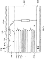
図4は、同時に継続中の米国特許出願番号09/970,758明細書に開示されている半導体パワーデバイスを示している。このデバイスでは、トレンチの断面を円形に形成しており、したがって、フローティングアイランドは、ドーナツ状の形状を有している。勿論、トレンチは、正方形、長方形又は六角形等、円形以外の形状を有していてもよく、このトレンチの断面形状がフローティングアイランドの形状を決定する。n+シリコン基板402上に形成されたn型エピタキシャルシリコン層401は、pボディ領域405aと、半導体デバイス内の2つのMOSFETセルに対応するn+ソース領域407とを備える。図4に示すように、pボディ領域405aは、深いpボディ領域405bを備えていてもよい。n+ソース領域407とボディ領域405aを接続するために、ソース及びボディ電極412がエピタキシャル層401の表面の特定の部分に広がっている。両セル用のn型ドレインは、半導体の上表面まで延びているn型エピタキシャル層401の一部によって形成される。ドレイン電極は、n+シリコン基板402の底部に設けられている。ボディのチャネル及びドレイン部分の上には、酸化層とポリシリコン層からなる絶縁ゲート電極418が形成されている。エピタキシャルシリコン層401によって画定される半導体デバイスの電圧維持領域内には、一連のフローティングアイランド410が形成されている。フローティングアイランド410は、半導体デバイスの上側から見て、アレー状に配列されている。例えば、図4に示す実施例では、「y軸」方向において、フローティングアイランドには、41011、41012、41013、・・・、4101mといった符号を付しており、「z軸」方向には、41011、41021、41031、410m1といった符号を付している。ゲート電極418の真下に位置するフローティングアイランド410の列は、設けても設けなくてもよく、これらは、半導体デバイスの幾何学的構造(geometry)及びエピタキシャル層410の抵抗率に対する要求に応じて設けられる。
FIG. 4 shows a semiconductor power device disclosed in co- pending US patent application Ser. No. 09 / 970,758 . In this device, the cross section of the trench is formed in a circular shape, and therefore the floating island has a donut shape. Of course, the trench may have a shape other than a circle, such as a square, a rectangle, or a hexagon, and the cross-sectional shape of the trench determines the shape of the floating island. The n-type
図4に示す半導体デバイスでは、フローティングアイランドの水平方向の行、例えばフローティングアイランド41011、41012、41013、・・・、4101Mからなる行は、それぞれ個別の打込み工程によって形成される。この製造方法では、例えば図3を用いて説明したような従来の製造方法に比べて、必要なエピタキシャル成長工程の回数を減らすことができるが、ここで、必要な打込み工程の回数を減らすことによって、より単純な製造方法を実現することが望まれる。 In the semiconductor device shown in FIG. 4, the horizontal line of the floating island, for example, a floating island 410 11, 410 12, 410 13, ..., the row of 410 1M, each of which is formed by a separate implantation step. In this manufacturing method, for example, the number of necessary epitaxial growth steps can be reduced as compared with the conventional manufacturing method as described with reference to FIG. 3, but here, by reducing the number of necessary implantation steps, It is desired to realize a simpler manufacturing method.
本発明では、p型フローティングアイランドを共通の軸を有する環状の棚(coaxially located annular ledges)として形成する。以下、このようなフローティングアイランドを半導体パワーデバイスの電圧維持層内に形成する手法について説明する。まず、半導体デバイスの電圧維持層となるエピタキシャル層内に雛壇状のトレンチ(terraced trench)を形成する。雛壇状のトレンチは、エピタキシャル層内の異なる深さにエッチングされた共通の軸を有する2つ以上のトレンチから形成される。各トレンチの直径は、エピタキシャル層において、各トレンチが、より深いトレンチよりも長い直径を有するように形成される。隣り合うトレンチは、水平面において連結され、隣り合うトレンチの直径の差の結果、環状の棚が画定される。p型の不純物は、1回の打込み工程によって、各環状の棚とトレンチにおける最も深い位置である底部とに同時に打ち込まれる。必要であれば、最下位のトレンチは、底部にドープ領域の環状リングを形成するように、更にエッチングしてもよい。打ち込まれた材料は、棚とトレンチの底部に隣接し及びこれらの下方の電圧維持領域内の部分に拡散する。これにより、打ち込まれた材料は、共通の軸を有する複数の環状リングとして、一連のフローティングアイランドを形成する。最後に、半導体デバイスの特性に悪い影響を与えない材料をトレンチに埋め込む。トレンチに埋め込む材料の具体例としては、高抵抗ポリシリコン、シリコン酸化物のような誘電体、又はこの他の材料及びこれらの材料の組合せがある。 In the present invention, p-type floating islands are formed as coaxially located annular ledges having a common axis. Hereinafter, a method for forming such a floating island in the voltage maintaining layer of the semiconductor power device will be described. First, a terraced trench is formed in an epitaxial layer that serves as a voltage maintaining layer of a semiconductor device. A platform-like trench is formed from two or more trenches having a common axis etched to different depths in the epitaxial layer. The diameter of each trench in the epitaxial layer, each trench is formed to have a diameter greater than the deeper trenches. Adjacent trenches are connected in a horizontal plane and an annular shelf is defined as a result of the difference in diameter of the adjacent trenches. The p-type impurity is simultaneously implanted into each annular shelf and the bottom, which is the deepest position in the trench, by a single implantation process. If necessary, the lowest of the trench, so as to form an annular ring doped region on the bottom may be further etched. The implanted material diffuses adjacent to the bottom of the shelves and trenches and below them in the voltage sustaining region. Thus, the implanted material, as a plurality of annular rings with a common axis, forming a series of floating island. Finally, a material that does not adversely affect the characteristics of the semiconductor device is embedded in the trench. Specific examples of the material embedded in the trench include high resistance polysilicon, dielectrics such as silicon oxide, or other materials and combinations of these materials.
本発明に基づく半導体パワーデバイスの製造工程の具体例について、図5(a)〜図5(f)を用いて説明する。 A specific example of the manufacturing process of the semiconductor power device according to the present invention will be described with reference to FIGS.
まず、従来と同様に、n+にドープされた基板502上に、n型エピタキシャル層501を成長させる。エピタキシャル層501の厚さは、抵抗率が5〜40Ωcm、400〜800Vの半導体デバイスでは、代表的に、15〜50μmである。次に、エピタキシャル層501の表面を誘電体層で覆うことによって、誘電体マスキング層を形成し、続いて周知の手法により、この誘電体マスキング層を、トレンチ5201の位置を画定するマスク部分を残して露光し、パターンを形成する。次に、反応性イオンエッチングによって、マスク開口部を介して、トレンチ5201を、例えば5〜15μmの深さにドライエッチングする。詳しくは、等間隔で設けられるフローティングアイランドの水平方向の行の所望の数を「x」とすると、トレンチ520は、まず、後に形成されるボディ領域の底部とn+にドープされた基板502の上面との間に存在するエピタキシャル層501の部分の厚さの約1/(x+1)の深さにエッチングする。ここで、必要に応じて、各トレンチ520の側壁を平滑にしてもよい。この場合、まず、反応性イオンエッチングプロセスによって生じた損傷を除去するために、トレンチ520の側壁から酸化物の薄膜層(通常500〜1000Å)を、化学的なドライエッチングによって取り除く。次に、犠牲二酸化シリコン層をトレンチ5201上に成長させる。そして、トレンチ5201の側壁を可能な限り平坦にするために、犠牲二酸化シリコン層を、バッファードフッ酸を用いたエッチング(buffered oxide etch)又はフッ化水素酸を用いたエッチング(HF etch)によって除去する。
First, an n-
次に、図5(b)に示すように、トレンチ5201内に二酸化シリコン層5241を成長させる。二酸化シリコン層(以下、酸化層とも呼ぶ。)5241の厚さは、このトレンチ5201と、次に形成されるトレンチとの間の直径の差(したがって、この結果形成される環状の棚の径方向の幅)を決定する。次に、トレンチ5201の底部から酸化層5241を取り除く。
Next, as shown in FIG. 5B, a
次に、図5(c)に示すように、トレンチ5201の露出された底部を介して、第2のトレンチ5202をエッチングする。この実施例では、トレンチ5202の厚さは、トレンチ5201の厚さと同じになるように形成する。すなわち、トレンチ5202は、ボディ領域の底部とn+にドープされた基板502の上面との間に存在するエピタキシャル層501の部分の厚さの約1/(x+1)の深さにエッチングする。これにより、トレンチ5202の底部は、ボディ領域の底部から2/(x+1)の深さに位置することとなる。
Next, as shown in FIG. 5 (c), via the exposed bottom of the
次に、図5(d)に示すように、まず、トレンチ5202の壁に酸化層5242を成長させることによって、第3のトレンチ5203(図5(e)及び図5(f)に最も明瞭に示されている。)を形成する。ここでも、二酸化シリコン層5242の厚さは、トレンチ5202と、トレンチ5203との間の直径の差(したがって、この結果形成される環状の棚の径方向の幅)を決定する。次に、トレンチ5202の底部から酸化層5242を取り除く。このプロセスは、所望の数のトレンチが形成され、したがって、所望の数の環状の棚が形成できるようになるまで、必要な回数繰り返し行われる。例えば、図5(d)では、4個のトレンチ5201〜5204(図5(e)に最も明瞭に示されている。)が形成されている。
Next, as shown in FIG. 5 (d), first, by growing an
次に、図5(e)に示すように、4個のトレンチ5201〜5204の側壁に形成された各酸化層をエッチングによって取り除くことにより、環状の棚5461〜5463を形成する。次に、トレンチ5201〜5204内に、略均一の厚さを有する酸化層540を形成する。酸化層540の厚さは、打込み原子が、トレンチ5201〜5204の側壁に隣接するシリコンに透過することを防止するのに十分な厚さであって、且つ環状の棚5461〜5463及びトレンチ底部555において、打込み原子が酸化層540の一部を透過できる厚さにする必要がある。
Next, as shown in FIG. 5 (e), by removing the respective oxide layer formed on the sidewalls of four trenches 520 1-520 4 by etching, to form the shelf 546 1-546 3 cyclic. Next, an
トレンチ5201〜5204の直径は、最終的に形成される環状の棚5461〜5463及びトレンチ底部555が同じ表面積を有するように選択する。これにより、環状の棚5461〜5463及びトレンチ底部555に不純物が打ち込まれると、この結果形成される各フローティングアイランドの水平面は、同じ電荷を有するようになる。
The diameters of the trenches 520 1 -520 4 are selected so that the finally formed annular shelves 546 1 -546 3 and the
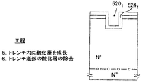
次に、図5(f)に示すように、棚5461〜5463及びトレンチ底部555に設けられた酸化層540を介して、ホウ素等の不純物を打ち込む。不純物の総ドーズ量は及び打込みエネルギは、後に拡散工程を行った後に、エピタキシャル層501に残留する不純物の量が、最終的な半導体デバイスで要求される降伏電圧を満足するように、選択される。次に、高温拡散工程を行い、先に打ち込まれた不純物528を縦方向(vertically)及び横方向(laterally)にドライブイン(drive-in)し、これにより共通の軸を有するフローティングアイランド5501〜5504を形成する。
Next, as shown in FIG. 5F, impurities such as boron are implanted through the
次に、半導体デバイスの特性に悪影響を与えない材料を、個々のトレンチ5201〜5204から形成された雛壇状のトレンチに埋め込む。このような材料としては、以下に限定されるものではないが、例えば、熱成長される二酸化シリコン、及び二酸化シリコン、窒化シリコンのような堆積される誘電体、並びにこれらの又は他の材料の熱成長層及び堆積層の組合せ等がある。そして、図5(f)に示すように、この構造体の表面を平坦化(planarize)する。図5(g)は、図5(f)と同様の構造において、トレンチ底部を更にエッチングし、この底部に不純物を含む底部環状リングを形成した構成例を示している。 Next, a material that does not adversely affect the properties of semiconductor devices, embedded in terraced trench formed from individual trench 520 1-520 4. Such materials include, but are not limited to, thermally grown silicon dioxide, and deposited dielectrics such as silicon dioxide, silicon nitride, and the heat of these or other materials. There are combinations of growth layers and deposition layers. Then, as shown in FIG. 5F, the surface of the structure is planarized. FIG. 5G shows a configuration example in which the bottom of the trench is further etched and a bottom annular ring containing impurities is formed at the bottom in the same structure as in FIG.
図5(f)及び図5(g)に示す構造体を製造する上述した処理工程のシーケンスにより、数多くの様々な半導体パワーデバイスに一連の環状のフローティングアイランドを有する電圧維持領域を作ることができる。上述のように、このような電力用半導体素子としては、DMOS、V溝DMOS、トレンチDMOS、MOSFET、IGBT、及びこの他のMOSゲートデバイスが含まれる。例えば、図4は、図5に示す電圧維持領域上に形成することができるMOSFETの具体例を示している。なお、図5(a)〜図5(g)では、単一の雛壇状のトレンチを示しているが、本発明では、単一又は複数の雛壇状のトレンチを用いて、いかなる数のフローティングアイランドの列を形成してもよい。 The sequence of processing steps described above for manufacturing the structure shown in FIGS. 5 (f) and 5 (g) can create a voltage sustaining region having a series of annular floating islands in many different semiconductor power devices. . As described above, such power semiconductor elements include DMOS, V-groove DMOS, trench DMOS, MOSFET, IGBT, and other MOS gate devices. For example, FIG. 4 shows a specific example of a MOSFET that can be formed on the voltage maintaining region shown in FIG. 5 (a) to 5 (g) show a single platform-like trench, but in the present invention, any number of floating islands can be formed using a single or a plurality of platform-like trenches. May be formed.
図5に示すような電圧維持領域及びフローティングアイランドを形成した後、次のような工程によって、図4に示すようなMOSFETが完成する。まず、アクティブ領域のマスクを形成した後、ゲート酸化層を成長させる。次に、多結晶シリコンを堆積させ、不純物をドープし、酸化させる。次に、ポリシリコン層をマスクし、ゲート領域を形成する。次に、従来と同様のマスキング工程、打込み工程及び拡散工程を用いて、深いp+にドープされたボディ領域405bを形成する。深いp+にドープされたボディ領域405bは、例えば、20〜200KeVで、ドーズ量を約1×10¹⁴〜5×10¹⁵/cm2として、ホウ素を打ち込む。同様の手法により、浅いボディ領域405aも形成する。浅いボディ領域405aには、20〜100KeVで、ドーズ量を約1×1013〜5×1014/cm2として、ホウ素を打ち込む。
After the voltage maintaining region and the floating island as shown in FIG. 5 are formed, the MOSFET as shown in FIG. 4 is completed through the following steps. First, after forming an active region mask, a gate oxide layer is grown. Next, polycrystalline silicon is deposited, doped with impurities, and oxidized. Next, the polysilicon layer is masked to form a gate region. Next, a
次に、フォトレジストマスキングプロセスによって、ソース領域407を画定するパターンのマスク層を形成する。続いて、打込み及び拡散によって、ソース領域407を形成する。ソース領域407には、例えば、20〜100KeVで、代表的には2×10¹⁵〜1.2×10¹⁶/cm2の濃度でヒ素を打ち込む。打込みの後、ヒ素は、約0.5〜2.0μmの深さに拡散する。ボディ領域405aの深さは、代表的には約1〜3μmとし、深いp+にドープされたボディ領域405bは、(これを設ける場合は)これよりも若干深く形成する。最後に、従来の方法でマスク層を除去する。DMOSトランジスタは、従来の方法で酸化層を形成及びパターン化し、コンタクト開口部(contact opening)を形成することにより完成する。更に、金属層を蒸着させ、マスキングして、ソース及びボディ領域とゲート電極とを画定する。マスクは、パッドコンタクトを画定するためにも使用する。そして、基板402の底面にドレインコンタクト層を形成する。
Next, a mask layer having a pattern defining the
ここでは、パワーMOSFETを製造するための特定の一連のプロセスについて説明したが、本発明の範囲内で他のプロセスを用いることもできる。例えば、深いp+にドープされたボディ領域405bは、ゲート領域を画定する前に形成してもよい。更に、トレンチを形成する前に、深いp+にドープされたボディ領域405bを形成してもよい。幾つかのDMOS構造では、p+にドープされたボディ領域は、p−にドープされたボディ領域よりも浅く形成してもよく、更に幾つかの具体例では、p+にドープされたボディ領域を設けなくてもよい。
Although a specific series of processes for manufacturing a power MOSFET has been described herein, other processes can be used within the scope of the present invention. For example, the deep p + doped
以上、様々な実施例を詳細に図示し、説明したが、上述の説明から、本発明に基づくこれらの実施例を修正及び変更することができ、このような修正及び変更は、請求の範囲に基づく本発明の主旨及び範囲から逸脱するものではない。特定の一実施例においては、本発明に基づく方法を用いて、各半導体領域の伝導性が上述の実施例とは逆の半導体パワーデバイスを製造することもできる。更に、本発明に基づく半導体パワーデバイスを製造するために必要な工程を縦型DMOSトランジスタを例に説明したが、ここに開示した手法を用いて、例えばダイオード、バイポーラトランジスタ、パワーJFET、IGBT、MCT及びこの他のMOSゲートパワーデバイスを始めとするこの他のDMOS FET及びこの他の半導体パワーデバイスを製造することもできる。 While various embodiments have been shown and described in detail, from the foregoing description, these embodiments according to the invention can be modified and changed, and such modifications and changes are within the scope of the claims. There is no departure from the spirit and scope of the present invention. In one particular embodiment, the method according to the present invention can be used to produce a semiconductor power device in which the conductivity of each semiconductor region is the opposite of that described above. Further, the steps necessary for manufacturing the semiconductor power device according to the present invention have been described by taking a vertical DMOS transistor as an example. By using the technique disclosed herein, for example, a diode, a bipolar transistor, a power JFET, an IGBT, an MCT And other DMOS FETs and other semiconductor power devices, including other MOS gate power devices.
Claims (39)
B.
1.上記基板上に、第1の伝導型を有するエピタキシャル層を成長させる工程と、
2.上記エピタキシャル層内に、2つ以上のトレンチを異なる深さにエッチングすることによって、幅が異なる複数の部分を有し、該各部分間に環状の棚を画定する少なくとも1つの雛壇状のトレンチを形成する工程と、
3.上記トレンチの壁及び底部に沿ってバリア材を堆積させる工程と、
4.上記環状の棚及び上記トレンチの底部に堆積された上記バリア材を介して、上記エピタキシャル層の隣接する部分に、第2の伝導型の不純物を打ち込む工程と、
5.上記不純物を拡散させて、上記エピタキシャル層内に少なくとも1つの環状のドープ領域と、該エピタキシャル層内の該環状のドープ領域の下方に位置する少なくとも1つの他の領域とを形成する工程と、
6.上記雛壇状のトレンチ内に誘電体材料を堆積させて、該雛壇状のトレンチを埋め込む工程と
によって、上記基板上のエピタキシャル層内に電圧維持領域を形成する工程と、
C.上記電圧維持領域上に、第2の伝導型の領域を少なくとも1つ形成し、該第2の伝導型の領域と該電圧維持領域との間に接合を画定する工程とを有する半導体パワーデバイスの製造方法。A. Preparing a first conductivity type substrate;
B.
1. Growing an epitaxial layer having a first conductivity type on the substrate;
2. In the epitaxial layer by etching two or more trenches at a depth different, having a plurality of portions different widths, at least one terraced trench defining an annular ledge between the respective parts Forming, and
3. Depositing a barrier material along the walls and bottom of the trench;
4). Through shelves and the barrier material deposited on the bottom of the trench of the annular, the adjacent portions of the epitaxial layer, a step of implanting second conductivity type impurities,
5. By diffusing the impurity, and forming at least one annular doped region, and at least one other region located below the annular doped regions of the epitaxial layer in the epitaxial layer,
6). Depositing a dielectric material in said terraced trench, by burying the該雛altar shaped trenches, forming a voltage sustaining region in the epitaxial layer on said substrate,
C. To the voltage sustaining region, the region of the second conductivity type and at least one formation, the semiconductor power device and a step of defining a junction between said second conductivity type region and the voltage sustaining region Production method.
上記エピタキシャル層内の上記電圧維持領域上に、上記第2の伝導型を有する第1及び第2のボディ領域を形成し、該第1及び第2のボディ領域間にドリフト領域を画定する工程と、
上記第1及び第2のボディ領域内に、上記第1の伝導型の第1及び第2のソース領域をそれぞれ形成する工程とを更に有することを特徴とする請求項1記載の半導体パワーデバイスの製造方法。Step C above, the
Forming first and second body regions having the second conductivity type on the voltage maintaining region in the epitaxial layer, and defining a drift region between the first and second body regions; ,
To the first and second body region of a semiconductor power device according to claim 1, further comprising the step of forming said first conductivity type first and second source regions of the respective Production method.
xを上記電圧維持領域に形成する環状のドープ領域の所定数以上の整数として、上記雛壇状のトレンチの複数の部分のうちの第1の部分を、上記所定の厚さの1/(x+1)に等しい距離分エッチングする工程を更に有する請求項1記載の半導体パワーデバイスの製造方法。The epitaxial layer has a predetermined thickness,
x as a predetermined number or more integer annular doped regions you formed in the voltage sustaining region, the first portion of the plurality of portions of the terraced trench, of the predetermined thickness 1 / (x + 1 The method of manufacturing a semiconductor power device according to claim 1, further comprising a step of etching by a distance equal to.
上記基板上に成長された第1の伝導型を有するエピタキシャル層内に形成された電圧維持領域と、
上記電圧維持領域上に形成され、第2の伝導性を有し、該電圧維持領域との間に接合を画定する少なくとも1つのアクティブ領域とを備え、
上記電圧維持領域は、
上記エピタキシャル層内に、2つ以上のトレンチを異なる深さにエッチングすることによって形成された、幅が異なる複数の部分を有し、該部分間に1つの環状の棚を画定する少なくとも1つの雛壇状のトレンチと、
上記エピタキシャル層内の上記環状の棚の下方の及び隣接する部分に形成された、第2の伝導型の不純物がドープされた少なくとも1つの環状のドープ領域と、
上記雛壇状のトレンチに埋め込まれた誘電体材料とを有することを特徴とする半導体パワーデバイス。 A substrate of a first conductivity type ;
A voltage sustaining region formed in the epitaxial layer having a first conductivity type grown on said substrate,
At least one active region formed on the voltage sustaining region and having a second conductivity and defining a junction with the voltage sustaining region ;
The voltage maintenance region is
In the epitaxial layer, two or more trenches formed by etching at different depths, a plurality of portions different widths, at least one terraced defining a shelf one annular to the site minutes Shaped trench,
At least one annular doped region doped with an impurity of a second conductivity type formed below and adjacent to the annular shelf in the epitaxial layer;
A semiconductor power device comprising: a dielectric material embedded in the trapezoidal trench.
上記雛壇状のトレンチの複数の部分のそれぞれは、xを上記電圧維持領域に形成する環状のドープ領域の所定数以上の整数として、上記所定の厚さの1/(x+1)に等しい距離分エッチングされて形成されることを特徴とする請求項26記載の半導体パワーデバイス。The epitaxial layer has a predetermined thickness,
Each of the plurality of portions of the terraced trench, the x as a predetermined number or more integer annular doped regions you formed in the voltage sustaining region, the distance equal amount 1 / of the predetermined thickness (x + 1) the semiconductor power device of claim 26, wherein Rukoto formed by etching.
上記エピタキシャル層内の上記電圧維持層上に形成され、第2の伝導型を有し、ドリフト領域を画定する第1及び第2のボディ領域と、
上記第1及び第2のボディ領域内にそれぞれ形成された第1の導電型の第1及び第2のソース領域とを更に有することを特徴とする請求項26記載の半導体パワーデバイス。Said at least one active region,
First and second body regions formed on the voltage sustaining layer in the epitaxial layer, having a second conductivity type and defining a drift region;
27. The semiconductor power device according to claim 26 , further comprising first and second source regions of the first conductivity type formed in the first and second body regions, respectively.
Applications Claiming Priority (2)
| Application Number | Priority Date | Filing Date | Title |
|---|---|---|---|
| US09/970,758 US6649477B2 (en) | 2001-10-04 | 2001-10-04 | Method for fabricating a power semiconductor device having a voltage sustaining layer with a terraced trench facilitating formation of floating islands |
| PCT/US2002/031790 WO2003030220A2 (en) | 2001-10-04 | 2002-10-03 | Method for fabricating a power semiconductor device having a voltage sustaining layer with a terraced trench facilitating formation of floating islands |
Publications (2)
| Publication Number | Publication Date |
|---|---|
| JP2005505918A JP2005505918A (en) | 2005-02-24 |
| JP4615217B2 true JP4615217B2 (en) | 2011-01-19 |
Family
ID=25517468
Family Applications (1)
| Application Number | Title | Priority Date | Filing Date |
|---|---|---|---|
| JP2003533321A Expired - Fee Related JP4615217B2 (en) | 2001-10-04 | 2002-10-03 | Method for manufacturing a semiconductor power device having a voltage sustaining layer having a trapezoidal trench for forming a floating island |
Country Status (9)
| Country | Link |
|---|---|
| US (2) | US6649477B2 (en) |
| EP (1) | EP1433200B1 (en) |
| JP (1) | JP4615217B2 (en) |
| KR (1) | KR100916818B1 (en) |
| CN (1) | CN100568466C (en) |
| AU (1) | AU2002347807A1 (en) |
| DE (1) | DE60239692D1 (en) |
| TW (1) | TW561628B (en) |
| WO (1) | WO2003030220A2 (en) |
Families Citing this family (26)
| Publication number | Priority date | Publication date | Assignee | Title |
|---|---|---|---|---|
| US7303810B2 (en) | 2001-03-05 | 2007-12-04 | 3Form, Inc. | Fire-resistant architectural resin materials |
| US7736976B2 (en) | 2001-10-04 | 2010-06-15 | Vishay General Semiconductor Llc | Method for fabricating a power semiconductor device having a voltage sustaining layer with a terraced trench facilitating formation of floating islands |
| US6576516B1 (en) * | 2001-12-31 | 2003-06-10 | General Semiconductor, Inc. | High voltage power MOSFET having a voltage sustaining region that includes doped columns formed by trench etching and diffusion from regions of oppositely doped polysilicon |
| US6656797B2 (en) * | 2001-12-31 | 2003-12-02 | General Semiconductor, Inc. | High voltage power MOSFET having a voltage sustaining region that includes doped columns formed by trench etching and ion implantation |
| US6686244B2 (en) | 2002-03-21 | 2004-02-03 | General Semiconductor, Inc. | Power semiconductor device having a voltage sustaining region that includes doped columns formed with a single ion implantation step |
| JP4500530B2 (en) * | 2003-11-05 | 2010-07-14 | トヨタ自動車株式会社 | Insulated gate semiconductor device and manufacturing method thereof |
| JP4241444B2 (en) * | 2004-03-10 | 2009-03-18 | 富士雄 舛岡 | Manufacturing method of semiconductor device |
| JP4491307B2 (en) * | 2004-09-21 | 2010-06-30 | トヨタ自動車株式会社 | Semiconductor device and manufacturing method thereof |
| US20070012983A1 (en) * | 2005-07-15 | 2007-01-18 | Yang Robert K | Terminations for semiconductor devices with floating vertical series capacitive structures |
| US7880224B2 (en) * | 2008-01-25 | 2011-02-01 | Infineon Technologies Austria Ag | Semiconductor component having discontinuous drift zone control dielectric arranged between drift zone and drift control zone and a method of making the same |
| CN102468177A (en) * | 2010-11-19 | 2012-05-23 | 无锡华润上华半导体有限公司 | P-type doubled diffusion metal-oxide-semiconductor (DMOS) device and making method thereof |
| CN102306657A (en) * | 2011-10-13 | 2012-01-04 | 电子科技大学 | Insulated gate bipolar transistor with floating buried layer |
| US8765609B2 (en) | 2012-07-25 | 2014-07-01 | Power Integrations, Inc. | Deposit/etch for tapered oxide |
| KR101367491B1 (en) * | 2012-08-08 | 2014-02-26 | 고려대학교 산학협력단 | Method for manufacturing semiconductor device having a single floating island and semiconductor device manufactured thereby |
| CN108922872A (en) * | 2018-07-09 | 2018-11-30 | 盛世瑶兰(深圳)科技有限公司 | A kind of power device chip and preparation method thereof |
| US10886226B2 (en) * | 2018-07-31 | 2021-01-05 | Taiwan Semiconductor Manufacturing Co, Ltd. | Conductive contact having staircase barrier layers |
| CN109273439A (en) * | 2018-09-14 | 2019-01-25 | 深圳市心版图科技有限公司 | A kind of power device protection chip and preparation method thereof |
| FR3086797B1 (en) * | 2018-09-27 | 2021-10-22 | St Microelectronics Tours Sas | ELECTRONIC CIRCUIT INCLUDING DIODES |
| CN109244071B (en) * | 2018-09-29 | 2021-06-18 | 深圳市物芯智能科技有限公司 | Power device protection chip and preparation method thereof |
| CN109300893A (en) * | 2018-09-29 | 2019-02-01 | 深圳市南硕明泰科技有限公司 | Power device protects chip and preparation method thereof |
| CN113629144B (en) * | 2020-05-08 | 2023-07-07 | 长鑫存储技术有限公司 | Semiconductor device and method for manufacturing the same |
| KR102369050B1 (en) * | 2020-06-30 | 2022-03-02 | 현대모비스 주식회사 | Power semiconductor device and method of fabricating the same |
| DE102021113288A1 (en) | 2020-05-22 | 2021-11-25 | Hyundai Mobis Co., Ltd. | POWER SEMI-CONDUCTOR DEVICE AND METHOD FOR MANUFACTURING IT |
| CN111725318B (en) * | 2020-06-18 | 2024-04-09 | 湖南国芯半导体科技有限公司 | Cell structure of power semiconductor device and manufacturing method thereof |
| US11361971B2 (en) | 2020-09-25 | 2022-06-14 | Taiwan Semiconductor Manufacturing Company, Ltd. | High aspect ratio Bosch deep etch |
| CN117650175B (en) * | 2024-01-30 | 2024-04-09 | 深圳市冠禹半导体有限公司 | Vertical GaN HEMT semiconductor device and manufacturing method thereof |
Family Cites Families (29)
| Publication number | Priority date | Publication date | Assignee | Title |
|---|---|---|---|---|
| US53568A (en) * | 1866-04-03 | Improvement in carriages | ||
| GB2089119A (en) * | 1980-12-10 | 1982-06-16 | Philips Electronic Associated | High voltage semiconductor devices |
| JPS5832430A (en) * | 1981-08-21 | 1983-02-25 | Toshiba Corp | Manufacture of semiconductor device |
| USH204H (en) * | 1984-11-29 | 1987-02-03 | At&T Bell Laboratories | Method for implanting the sidewalls of isolation trenches |
| US4719185A (en) * | 1986-04-28 | 1988-01-12 | International Business Machines Corporation | Method of making shallow junction complementary vertical bipolar transistor pair |
| US4893160A (en) * | 1987-11-13 | 1990-01-09 | Siliconix Incorporated | Method for increasing the performance of trenched devices and the resulting structure |
| JPH01136369A (en) * | 1987-11-21 | 1989-05-29 | Toshiba Corp | Manufacture of semiconductor device having overvoltage protective function |
| CN1019720B (en) | 1991-03-19 | 1992-12-30 | 电子科技大学 | Power semiconductor device |
| KR940009640B1 (en) * | 1991-12-13 | 1994-10-15 | 금성일렉트론 주식회사 | Manufacturing method and structure of dual trench capacitor cell |
| US5488236A (en) * | 1994-05-26 | 1996-01-30 | North Carolina State University | Latch-up resistant bipolar transistor with trench IGFET and buried collector |
| JPH08162547A (en) * | 1994-11-30 | 1996-06-21 | Toshiba Corp | Semiconductor memory |
| JP3291957B2 (en) * | 1995-02-17 | 2002-06-17 | 富士電機株式会社 | Vertical trench MISFET and method of manufacturing the same |
| EP1408554B1 (en) * | 1996-02-05 | 2015-03-25 | Infineon Technologies AG | Field effect controlled semiconductor component |
| US5719409A (en) * | 1996-06-06 | 1998-02-17 | Cree Research, Inc. | Silicon carbide metal-insulator semiconductor field effect transistor |
| US6097076A (en) * | 1997-03-25 | 2000-08-01 | Micron Technology, Inc. | Self-aligned isolation trench |
| JP3342412B2 (en) * | 1997-08-08 | 2002-11-11 | 三洋電機株式会社 | Semiconductor device and method of manufacturing the same |
| DE19830332C2 (en) * | 1998-07-07 | 2003-04-17 | Infineon Technologies Ag | Vertical semiconductor device with reduced electrical surface field |
| DE19843959B4 (en) * | 1998-09-24 | 2004-02-12 | Infineon Technologies Ag | Method for producing a semiconductor component with a blocking pn junction |
| US6078078A (en) * | 1998-10-01 | 2000-06-20 | Advanced Micro Devices, Inc. | V-gate transistor |
| US6194741B1 (en) * | 1998-11-03 | 2001-02-27 | International Rectifier Corp. | MOSgated trench type power semiconductor with silicon carbide substrate and increased gate breakdown voltage and reduced on-resistance |
| DE19854915C2 (en) * | 1998-11-27 | 2002-09-05 | Infineon Technologies Ag | MOS field effect transistor with auxiliary electrode |
| US6316336B1 (en) * | 1999-03-01 | 2001-11-13 | Richard A. Blanchard | Method for forming buried layers with top-side contacts and the resulting structure |
| US6191447B1 (en) * | 1999-05-28 | 2001-02-20 | Micro-Ohm Corporation | Power semiconductor devices that utilize tapered trench-based insulating regions to improve electric field profiles in highly doped drift region mesas and methods of forming same |
| US6380569B1 (en) * | 1999-08-10 | 2002-04-30 | Rockwell Science Center, Llc | High power unipolar FET switch |
| GB0010041D0 (en) * | 2000-04-26 | 2000-06-14 | Koninkl Philips Electronics Nv | Trench semiconductor device manufacture |
| KR100364803B1 (en) * | 2000-11-15 | 2002-12-16 | 주식회사 하이닉스반도체 | Method for manufacturing Nonvolatile Memory |
| US6468847B1 (en) * | 2000-11-27 | 2002-10-22 | Power Integrations, Inc. | Method of fabricating a high-voltage transistor |
| JP3963664B2 (en) * | 2001-06-22 | 2007-08-22 | 富士雄 舛岡 | Semiconductor memory device and manufacturing method thereof |
| US6686244B2 (en) * | 2002-03-21 | 2004-02-03 | General Semiconductor, Inc. | Power semiconductor device having a voltage sustaining region that includes doped columns formed with a single ion implantation step |
-
2001
- 2001-10-04 US US09/970,758 patent/US6649477B2/en not_active Expired - Lifetime
-
2002
- 2002-10-03 CN CNB028196570A patent/CN100568466C/en not_active Expired - Fee Related
- 2002-10-03 WO PCT/US2002/031790 patent/WO2003030220A2/en active Application Filing
- 2002-10-03 AU AU2002347807A patent/AU2002347807A1/en not_active Abandoned
- 2002-10-03 DE DE60239692T patent/DE60239692D1/en not_active Expired - Lifetime
- 2002-10-03 EP EP02784020A patent/EP1433200B1/en not_active Expired - Fee Related
- 2002-10-03 KR KR1020047004955A patent/KR100916818B1/en not_active IP Right Cessation
- 2002-10-03 TW TW091122863A patent/TW561628B/en active
- 2002-10-03 JP JP2003533321A patent/JP4615217B2/en not_active Expired - Fee Related
-
2003
- 2003-11-13 US US10/712,810 patent/US7304347B2/en not_active Expired - Fee Related
Also Published As
| Publication number | Publication date |
|---|---|
| WO2003030220A2 (en) | 2003-04-10 |
| EP1433200A2 (en) | 2004-06-30 |
| TW561628B (en) | 2003-11-11 |
| US20030068854A1 (en) | 2003-04-10 |
| US20040097028A1 (en) | 2004-05-20 |
| JP2005505918A (en) | 2005-02-24 |
| EP1433200A4 (en) | 2009-03-11 |
| KR20040037243A (en) | 2004-05-04 |
| US6649477B2 (en) | 2003-11-18 |
| AU2002347807A1 (en) | 2003-04-14 |
| CN1565051A (en) | 2005-01-12 |
| US7304347B2 (en) | 2007-12-04 |
| KR100916818B1 (en) | 2009-09-14 |
| CN100568466C (en) | 2009-12-09 |
| DE60239692D1 (en) | 2011-05-19 |
| WO2003030220A3 (en) | 2004-02-12 |
| EP1433200B1 (en) | 2011-04-06 |
Similar Documents
| Publication | Publication Date | Title |
|---|---|---|
| JP4743744B2 (en) | Semiconductor power device having a floating island voltage sustaining layer | |
| JP4615217B2 (en) | Method for manufacturing a semiconductor power device having a voltage sustaining layer having a trapezoidal trench for forming a floating island | |
| JP4786872B2 (en) | Power semiconductor devices having voltage sustaining regions including doped columns formed by a single ion implantation process and methods for their manufacture | |
| JP4833517B2 (en) | Method of manufacturing a high voltage power MOSFET having a voltage sustaining region including a doped column formed by rapid diffusion | |
| US7736976B2 (en) | Method for fabricating a power semiconductor device having a voltage sustaining layer with a terraced trench facilitating formation of floating islands | |
| JP4741187B2 (en) | High voltage power MOSFET including doped column |
Legal Events
| Date | Code | Title | Description |
|---|---|---|---|
| A621 | Written request for application examination |
Free format text: JAPANESE INTERMEDIATE CODE: A621 Effective date: 20050914 |
|
| A131 | Notification of reasons for refusal |
Free format text: JAPANESE INTERMEDIATE CODE: A131 Effective date: 20090908 |
|
| A601 | Written request for extension of time |
Free format text: JAPANESE INTERMEDIATE CODE: A601 Effective date: 20091208 |
|
| A602 | Written permission of extension of time |
Free format text: JAPANESE INTERMEDIATE CODE: A602 Effective date: 20091215 |
|
| A601 | Written request for extension of time |
Free format text: JAPANESE INTERMEDIATE CODE: A601 Effective date: 20100108 |
|
| A602 | Written permission of extension of time |
Free format text: JAPANESE INTERMEDIATE CODE: A602 Effective date: 20100118 |
|
| A601 | Written request for extension of time |
Free format text: JAPANESE INTERMEDIATE CODE: A601 Effective date: 20100208 |
|
| A602 | Written permission of extension of time |
Free format text: JAPANESE INTERMEDIATE CODE: A602 Effective date: 20100216 |
|
| A521 | Written amendment |
Free format text: JAPANESE INTERMEDIATE CODE: A523 Effective date: 20100308 |
|
| TRDD | Decision of grant or rejection written | ||
| A01 | Written decision to grant a patent or to grant a registration (utility model) |
Free format text: JAPANESE INTERMEDIATE CODE: A01 Effective date: 20100921 |
|
| A01 | Written decision to grant a patent or to grant a registration (utility model) |
Free format text: JAPANESE INTERMEDIATE CODE: A01 |
|
| A61 | First payment of annual fees (during grant procedure) |
Free format text: JAPANESE INTERMEDIATE CODE: A61 Effective date: 20101020 |
|
| R150 | Certificate of patent or registration of utility model |
Free format text: JAPANESE INTERMEDIATE CODE: R150 |
|
| FPAY | Renewal fee payment (event date is renewal date of database) |
Free format text: PAYMENT UNTIL: 20131029 Year of fee payment: 3 |
|
| R250 | Receipt of annual fees |
Free format text: JAPANESE INTERMEDIATE CODE: R250 |
|
| R250 | Receipt of annual fees |
Free format text: JAPANESE INTERMEDIATE CODE: R250 |
|
| LAPS | Cancellation because of no payment of annual fees |