JP4608040B2 - Semiconductor laser device - Google Patents
Semiconductor laser device Download PDFInfo
- Publication number
- JP4608040B2 JP4608040B2 JP21691699A JP21691699A JP4608040B2 JP 4608040 B2 JP4608040 B2 JP 4608040B2 JP 21691699 A JP21691699 A JP 21691699A JP 21691699 A JP21691699 A JP 21691699A JP 4608040 B2 JP4608040 B2 JP 4608040B2
- Authority
- JP
- Japan
- Prior art keywords
- layer
- layers
- dopant
- laser device
- refractive index
- Prior art date
- Legal status (The legal status is an assumption and is not a legal conclusion. Google has not performed a legal analysis and makes no representation as to the accuracy of the status listed.)
- Expired - Fee Related
Links
Images

Classifications
-
- H—ELECTRICITY
- H01—ELECTRIC ELEMENTS
- H01S—DEVICES USING THE PROCESS OF LIGHT AMPLIFICATION BY STIMULATED EMISSION OF RADIATION [LASER] TO AMPLIFY OR GENERATE LIGHT; DEVICES USING STIMULATED EMISSION OF ELECTROMAGNETIC RADIATION IN WAVE RANGES OTHER THAN OPTICAL
- H01S5/00—Semiconductor lasers
- H01S5/30—Structure or shape of the active region; Materials used for the active region
-
- H—ELECTRICITY
- H01—ELECTRIC ELEMENTS
- H01S—DEVICES USING THE PROCESS OF LIGHT AMPLIFICATION BY STIMULATED EMISSION OF RADIATION [LASER] TO AMPLIFY OR GENERATE LIGHT; DEVICES USING STIMULATED EMISSION OF ELECTROMAGNETIC RADIATION IN WAVE RANGES OTHER THAN OPTICAL
- H01S5/00—Semiconductor lasers
- H01S5/10—Construction or shape of the optical resonator, e.g. extended or external cavity, coupled cavities, bent-guide, varying width, thickness or composition of the active region
- H01S5/18—Surface-emitting [SE] lasers, e.g. having both horizontal and vertical cavities
- H01S5/183—Surface-emitting [SE] lasers, e.g. having both horizontal and vertical cavities having only vertical cavities, e.g. vertical cavity surface-emitting lasers [VCSEL]
- H01S5/18361—Structure of the reflectors, e.g. hybrid mirrors
-
- H—ELECTRICITY
- H01—ELECTRIC ELEMENTS
- H01S—DEVICES USING THE PROCESS OF LIGHT AMPLIFICATION BY STIMULATED EMISSION OF RADIATION [LASER] TO AMPLIFY OR GENERATE LIGHT; DEVICES USING STIMULATED EMISSION OF ELECTROMAGNETIC RADIATION IN WAVE RANGES OTHER THAN OPTICAL
- H01S5/00—Semiconductor lasers
- H01S5/30—Structure or shape of the active region; Materials used for the active region
- H01S5/305—Structure or shape of the active region; Materials used for the active region characterised by the doping materials used in the laser structure
- H01S5/3054—Structure or shape of the active region; Materials used for the active region characterised by the doping materials used in the laser structure p-doping
- H01S5/3063—Structure or shape of the active region; Materials used for the active region characterised by the doping materials used in the laser structure p-doping using Mg
Description
【0001】
【発明の属する技術分野】
本発明は、一般に、半導体装置及びその製造に関し、特に、半導体レーザ装置などの発光素子に関するものである。そして、本発明は、とりわけ、垂直空洞面発光レーザ(VCSEL)装置に適用可能なものである。
【0002】
【従来の技術】
VCSEL装置等の半導体レーザ装置は、電流を流すと単色のコヒーレント光を発生する。基本的に、VCSELは、2つの反射層の間に挟まれた発光材料の層から構成される。
【0003】
熱放散は、VCSELの設計者が対処しなければならない難題の1つである。発生する熱の量は、VCSELの抵抗、及び、VCSELを流れる電流の量に関連している。抵抗は、電流が直列層を流れるので、一般に、「直列抵抗」と呼ばれる。VCSELは、できるだけ多くの電流を通すことによって、レーザ光の出力強度を最大にできることが望ましいが、加熱により通電量が制限される。
【0004】
従来のアプローチを利用すると、VCSEL構造の熱放散効率が低下した。例えば、図1に関連して後述する、Kish,Jr.他に対する米国特許第5,724,376号の明細書には、活性層に近接したヒート・シンクを用いる構造の解説がある。
【0005】
反射構造を構成する層の抵抗は、ドーピングによって小さくすることが可能であることも分かっている。これによって、所定の量の加熱に関して、より多くの電流を流すことが可能になるので、光出力強度が増大する。例えば、K.L.Lear他による「Low Threshold Voltage Vertical Cavity Surface−Emitting Laser」,Electronics Letters,Vol.29,No.7,(April1,1993),pp584−6を参照されたい。
【0006】
また、P.Zhou他による「Low Series ResistanceHigh−Efficiency GaAs/AlGaAs Vertical−Cavity Surface−Emitting Lasers with Continuously Graded Mirrors Grown by MOCVD」,IEEE Photonics Technology Letters,Vol.3,No.7(July 1991)には、反射層間の傾斜インターフェイスによって直流抵抗を小さくする技法が解説されている。
【0007】
【発明が解決しようとする課題】
本発明の目的は、通電能力をいっそう向上させ、同時に、抵抗を制限して、良好な製造性をもたらす新規なVCSEL構造を提供することにある。
【0008】
【課題を解決するための手段】
本発明によれば、直列抵抗が小さく、製造が容易な半導体レーザ装置が得られる。
【0009】
こうした半導体レーザ装置には、活性層と、活性層の両側に配置された第1と第2の反射構造が含まれている。第1と第2の反射構造は、それぞれ、分布ブラッグ反射装置(DBR)であり、各DBRには、それぞれ、(i)第1の屈折率を備えた第1の層と、(ii)第2の屈折率を備えた第2の層が含まれている。
【0010】
2つのDBRの一方にはpタイプ、もう一方には、nタイプのドーピングが施される。各DBR毎に、ドーピング・タイプは、一貫しているが、所定のDBRの異なる層には、異なるドーパントが用いられる。
【0011】
望ましい実施例の場合、反射構造は、AlGaAsから造られたDBRであるが、層の屈折率を変えるため、Al含有量は変更される。pタイプDBRの2つの層には、それぞれ、低屈折率層及び高屈折率層が得られるようにマグネシウムと炭素によるドーピングを施すのが望ましい。
【0012】
【発明の実施の形態】
本発明によれば、有機金属気相エピタキシ(OMVPE)によって、半導体VCSEL用のpタイプDBRを作製するために開発された協調ドーピング・プロセスが得られる。この協調ドーピング・プロセスを利用することによって、これらの装置で、低直列抵抗及び低動作電圧を実現し、良好な製造性を得られる。
【0013】
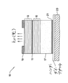
図1には、全体が10で表示された従来のVCSELの一例が示されている。図1のVCSELについては、後述するKish,Jr他に対する米国特許第5,724,376号の明細書に詳細な記載がある。
【0014】
VCSEL10などの半導体レーザでは、通電により発光する材料の層11が、活性材料として利用される。当該技術者には、この発光特性を備えた各種材料が知られている。
【0015】
対向する反射表面は、活性層の上方及び下方に製作される。上方反射構造13及び下方反射構造15が示されている。活性層11は、反射構造13、15の間に位置する。反射構造13及び15は、一般に、屈折率の異なる材料の層を順次堆積させることによって得られる。こうした構造は、分布ブラッグ反射装置(DBR)と呼ばれる。DBR間の間隙(活性層11によって占められる)は、ファブリ・ペロー空洞と呼ばれる。上記構造は、基板17上に形成される。
【0016】
VCSEL設計において、2つの反射構造13、15に互いに逆極性のドーピングを施すのが一般的である。すなわち、反射構造の一方には、nタイプのドーピングが施され、もう一方には、pタイプのドーピングが施される。従って、VCSELは、pn接合ダイオードに匹敵する特性を備えることが可能である。VCSELを用いた回路は、VCSELの2つの端子間に順バイアス電圧を印加してVCSELを駆動し、発光させる。
【0017】
半導体材料層の屈折率を設定する既知の方法がある。例えば、アルミニウム・ガリウム・砒素(AlGaAs)層を形成する場合、アルミニウム含有量を変えることが可能でアルミニウムの含有量が増すほど、屈折率は低下する。
【0018】
一般的なやり方に従って、nタイプまたはpタイプになるように、層にドーピングを施すことが可能である。例えば、炭素(C)またはマグネシウム(Mg)ドーパントを利用して、AlGaAsをpタイプにすることが可能である。
【0019】
上述の半導体構造に電流を供給して、活性層11を活性化するため、該構造の両側に電気接点19、21が設けられる。上部接点19は、レーザ光がVCSEL装置10から出射するための間隙が得られるように構成されている。図1に概略が示されている、可能性のある構成の1つでは、上部接点19には、レーザ光が通過する開口が設けられている。図1には、上昇して、上部接点19の開口を通るレーザ光が示されている。
【0020】
VCSEL10などのVCSEL装置は、接点19と21の間に特性抵抗を備えている。電流がVCSEL10を流れると、熱が発生する。熱は、ハンダ・ダイ・アタッチで取り付けられたヒート・シンク23によって放散される。
【0021】
図2は、本発明によるVCSEL装置の一部に関する概略図である。図2に示す構造は、図1の構造11、13、及び、15に対応する。図1の残りの部分には、本発明にとってあまり重要ではない構成要素が含まれている。従って、これらの補助的要素は、図2から省かれている。
【0022】
図1の活性層11と同様の活性層25は、2つの反射構造27及び29の間にVCSEL空洞を形成する。反射構造27及び29は、それぞれ、pタイプDBR及びnタイプDBRとして示されている。
【0023】
DBR27及び29には、屈折率の異なる2つの材料の交互層が含まれている。上述のように、材料がAlGaAsの場合、低Al組成のAlGaAs層は、高屈折率材料の働きをし、高Al組成のAlGaAs層は、低屈折率材料の働きをする。場合により、層間に不図示の傾斜インターフェイスを用いることも可能である。
【0024】
DBR内の1対の層は、単位下部構造とみなすことができる。そして、該下部構造を必要数用いてDBRを構成することが可能である。図2において、pタイプDBR27には、低屈折率層33及び高屈折率層35を含む、単位下部構造31が含まれている。
【0025】
DBR毎に1つのこうした単位下部構造は、理論的には最少であるが、実際には、DBRには、2つ以上の単位下部構造が含まれる。図示のように、単位下部構造をN1回繰り返すことによって、pタイプDBR27全体が形成される。同様に、nタイプDBR29には、N2回繰り返された単位下部構造37が含まれている。N1及びN2は、単位下部構造の総数を表す整数である。望ましい実施例の場合、N1及びN2は、約50にすることが可能である。
【0026】
全ての層を順次通過するポンプ電流は、構造の全抵抗に関連した熱を発生する。本発明によれば、全抵抗を小さくするため、層及びインターフェイスに十分なドーピングが施される。それによって、好都合なことには、DBR27及び29の両端間における電圧降下、及び、電流によって発生する熱が減少する。pタイプDBRは、nタイプDBRよりも抵抗が大きくなりがちである。従って、本発明は、とりわけ、pタイプDBRに適用するのに有利である。
【0027】
本発明によれば、「協調ドーピング」において、DBRまたはDBR単位下部構造の2つの層に異なるドーパントが用いられる。
【0028】
図2の構造には、Al含有量を変えることによって屈折率が変更される、望ましい材料AlGaAsから造られたDBRが含まれている。pタイプのAlGaAsによるDBRにおいて一般に用いられるドーパントのうちの2つは、MgとCである。pタイプDBR27の場合、Cは、層33のようなAl含有量の多いAlGaAs層のドーパントとして利用され、Mgは、層35のようなAl含有量の少ないAlGaAsに利用される。
【0029】
ちなみに、本発明の他の望ましい実施例の場合、Al含有量の多いAlGaAs層(例えば、層33)に、CとMgの組み合わせによるドーピング、並びに、Cだけのドーピングを施すことが可能である点に留意されたい。
【0030】
Mgは、AlGaAs材料のアルミニウム含有量に関係なくドーパントとして利用される。OMVPEによるMgドーピングは、既知のMgドーパント源を用いて実施される。
【0031】
しかし、Al組成の高いAlGaAsとインターフェイス層の場合、Mgには、活性化されるドーパント・イオンの可能性のある最高の濃度(すなわち、実現可能なキャリヤ濃度)が、あいにく、1018/cm3という低い値に制限される欠点がある。結果として、MgをドープしたpタイプDBRを利用して成長したVCSELは、直列抵抗が高くなるので、通常、動作電圧が高くなる。
【0032】
一方、炭素は、極めて高いレベルで、AlGaAs層に取り入れることが可能である。しかし、炭素をドーパントにしたOMVPEガスは、不都合な腐食性を備える傾向がある。周囲炭素ドーパント源ガスからドーピングを行うステップを含む製作プロセスの場合、炭素ドーパント源ガスによって、炭素をドープしたエピタキシャル層が堆積させられるAlGaAs層に対してバック・エッチが生じる。
【0033】
CBr4ドーパント・ガスが、Al含有量の少ないAlGaAsに用いられる場合、バック・エッチは、通常の成長速度の30%を超える速度で生じる。しかし、バック・エッチ速度は、AlAsのとって取るに足りないものである。AlとGaの両方を含む中間調合物の場合、バック・エッチ速度も中間である。さらに、バック・エッチ速度は、温度と、ウェーハを横切る気流パターンの変動に影響されやすい。
【0034】
結果として、CドープしたpタイプのDBRのウェーハ全域にわたる厚さの分布は、均一にならない傾向がある。対照的に、nタイプDBR構造の製作では、バック・エッチを生じる物質は用いられない。従って、nタイプDBRの製作は制御が容易であるが、pタイプDBRの製作には、DBRの厚さの不整合を生じる、均一性の問題がある。
【0035】
nタイプとpタイプのDBRが両方とも必要な従来のVCSELの場合、それらの間における厚さの不整合が、ウェーハ全域にわたる装置の性能の均一性を劣化させることになる。
【0036】
しかし、本発明によれば、アルミニウムの含有量が多く、従って、バック・エッチ及び結果生じる均一性の問題の影響を受けにくい材料の層だけに炭素のドーピングを利用することによって、より優れた均一性が得られる。炭素のドーピングは、Alの含有量が少なく、屈折率の高いAlGaAs層よりもAlの含有量が多く、屈折率の低いAlGaAs層に適している。
【0037】
よりバック・エッチの影響を受けやすい低Al層の場合、Mgドーピングは高Al材料に対する1cm3当たり1×10¹⁸という制限を受けない。こうして、バック・エッチの問題を生じることなく、両方の層において3×1018cm-3を超える高ドーピング濃度を容易に実現することが可能である。従って、Al含有量の少ない層のMgドーピングによって、バック・エッチ及び結果生じる不均一性を伴うことなく、構造全体に関して小さいことが望ましい抵抗と、及び、良好な製造性が得られる。
【0038】
本発明の望ましい実施例の1つでは、高Al層のドーピングに炭素だけしか用いないが、Mg及びCの混合物でドープすることも可能である。Alの含有量が多いので、ドーパント・ガスの炭素含有量によって、不利になるほどの量のバック・エッチが生じることはない。
図2の実施例、及び、技術者が以上の説明から認識するであろう関連実施例は、第1のクラスの実施例とみなすことができる。
【0039】
さらに2つの追加クラスの実施例(「第2」及び「第3」のクラス)が存在する。第2のクラスには、VCSEL空洞と前述の層の間にあるか、前記層に隣接するか、あるいは、前記層の間にある比較的狭いインターフェイス層も含まれる。これらのタイプの層を区別するため、「通常の」層という用語を用いて、上述の層を表すことにする。
【0040】
インターフェイス層によって、Al含有量の多い層からAl含有量の少ない層への組成の鋭い遷移が平滑になる。好都合なことには、これによって、直列抵抗が小さくなる。
【0041】
一般に、直列抵抗を十分に低減するには、インターフェイス層にかなりのドーピングを施すことが必要になる。このインターフェイス層における協調ドーピング設計(C+Mg、または、C単独)によって、好都合なことには、この抵抗の低減が実現する。
【0042】
第3のクラスの実施例の場合、層には、Al組成が連続変化するか、または、離散的なセクションへの分割、及び/または、異なるセクションへの協調ドーピングが施される。これは、通常の層で実施可能である。インターフェイス傾斜層も、セクションに分割し、それに従って協調ドーピングを施すことが可能である。
【0043】
インターフェイス層が設けられる場合、セクション化された協調ドーピングが、とりわけ有効であることが分かった。望ましいセクション化インターフェイスは、通常の層間で連結する役目をするAlGaAsのインターフェイス層が含まれている。1つまたは複数のインターフェイス層が、そのセクションに従ってコ・ドープされる。
【0044】
セクション・協調ドーピングは、多種多様なやり方で実施可能である。例えば、インターフェイス層は、2つのセクションを備えることが可能であり、そのうちの一方だけが協調ドーピングを施される。
【0045】
高Al層と低Al層が、それぞれ、インターフェイス層を備えている場合、協調ドーピングは低Al層の後インターフェイス層には施さず、高Al層の後のインターフェイス層に施すことが可能である。さらに、この層構成の場合、2つの通常の層自体は、協調ドーピングを施しても、施さなくてもかまわない。
【0046】
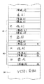
図3は、半導体レーザ装置の一例のpタイプDBRを示す断面図である。図3の装置は、第2のクラスの実施例によるインターフェイス層を備えており、このインターフェイス層は、第3のクラスの実施例によるセクション化協調ドーピングの一例を示している。
【0047】
図3には、全体が41で表示されたVCSEL空洞39及びpタイプDBRが示されている。簡略化のため、2つの単位下部構造43及び45が示されているが、もっと多くの単位下部構造が存在する可能性がある。単位下部構造43及び45には、それぞれ、Al含有量の多い通常の層(それぞれ、47及び49)と、Al含有量の少ない通常の層(それぞれ、51及び53)が含まれている。
【0048】
通常の層の間及び/または通常の層とVCSEL空洞39との間のインターフェイス層が、本発明の第2と第3の実施例を例示している。個々の例については、個別に論じることにする。
【0049】
第2のクラスの実施例に従って、インターフェイス層55は、VCSEL空洞39とAl含有量の多い通常層49との間に示されている。
【0050】
第3クラスの実施例に従って、セクション57及び59からなるインターフェイス層が、Al含有量の多い通常の層49とAl含有量の少ない通常の層53の間に示されている。以下の説明において、57及び59のような層は、互いに隣接する個別インターフェイス層、または、インターフェイス層全体のセクションと呼ぶことにする。どれがどちらの呼称になるかは、文脈から明らかになるであろう。
【0051】
図示のように、インターフェイス層55、57、及び、59は、通常の層53及び49よりも薄い。上述のように、55、57、及び、59のようなインターフェイス層が相対的に薄いことは、望ましい特徴である。
【0052】
また、インターフェイス層には、その相対的Al含有量を反映した説明もついている。Al含有量の説明は、直観的に分かる意味を有している。低Al(すなわち、Al含有量が最も少ない)から、準低Al、及び、準高Alを経て、高Al(すなわち、Al含有量が最も多い)に至るものと理解されたい。
【0053】
インターフェイス層の正確なAl組成は、用途に応じて変動する可能性があるが、本発明の第2と第3のクラスの実施例の望ましい実施例では、そのAl含有量が隣接するインターフェイス層または通常の層のAl含有量との中間値である層を備えている。例えば、順次隣接層が、49(高Al)から59(準高Al)及び57(準低Al)を経て53(低Al)に及んでいる。
【0054】
全体として捉えた図3の構造には、インターフェイス層が、pタイプDBR構造全体に組み込まれる望ましいやり方が示されている。すなわち、通常の層のそれぞれが、両側にインターフェイス層を備えている。
【0055】
例えば、下部構造45について詳細に検討することにする。インターフェイス層55及び59が、高Al通常層49の両側において隣接している。インターフェイス層55及び59は、それぞれ、準高Al含有量であるため、Al含有量は、層境界を越える際、比較的緩やかに変化する。また、低Al通常層53は、両側が、インターフェイス層57及びインターフェイス層61と隣接している。インターフェイス層57及び61は、準低Al含有量であり、従って、やはり、これらの層の境界を越えても、Al含有量は急激には変化しない。また、層57から層59への境界によって、Al含有量は準低から準高に変化するだけである。
【0056】
インターフェイス層の協調ドーピングは、やはり、本発明に従って行われる。例えば、個々のインターフェイス層のAl絶対含有量に従って、準低Al含有量インターフェイス層57及び61は、Mgをドープすることが可能であり、一方、準高Al含有量インターフェイス層55及び59は、C、または、C+Mgをドープすることが可能である。
【0057】
従って、本発明によれば、直列抵抗を最小にするためのドーピングを施されたDBR構造、及び、その製造にあたりバック・エッチの問題が回避される装置という、矛盾する要求が解決される。協調ドーピングを施されたDBRを備えるVCSELは、直列抵抗が小さく、動作電圧が低く、ウェーハ全域にわたって比較的均一性に優れるものと予測される。
本発明の広汎な応用に鑑み、以下に本発明の実施態様の一端を例示して参考に供する。
【0058】
(実施態様1):
両側を備える活性層(25)と、該活性層(25)の一方の側に配置されて、(i)第1の屈折率を備え、第1のドーパントを含む第1の半導体化合物から造られた第1の層(33)、及び、(ii)第2の屈折率を備え、第2のドーパントを含む第2の半導体化合物から造られた第2の層(35)を含む反射構造(27)が含まれている半導体レーザ装置。
【0059】
(実施態様2):
第1と第2の反射構造(27、29)のそれぞれについて、
第1の層(33)が、第1のIII−V半導体化合物から造られ、
第2の層(35)が、第2のIII−V半導体化合物から造られていることを特徴とする、実施態様1に記載の半導体レーザ装置。
【0060】
(実施態様3):
第1のIII−V半導体化合物(33)が、第1のAl組成のAlGaAsであり、第2のIII−V半導体化合物(35)が、第1のAl組成より低い第2のAl組成のAlGaAsであることを特徴とする実施態様2に記載の半導体レーザ装置。
【0061】
(実施態様4):
第1と第2の反射構造(27、29)のそれぞれについて、
第1の層(33)に、(i)炭素と、(ii)炭素及びマグネシウムからなるグループからの選択したドーパントがドープされ、
第2の層(35)に、マグネシウムがドープされていることを特徴とする実施態様2に記載の半導体レーザ装置。
【0062】
(実施態様5):
第1と第2の反射構造(27、29)のそれぞれに、さらに、それぞれ、(i)第1の屈折率を有し、第1のドーパントを含む第1の半導体化合物から造られた第3の層と、(ii)第2の屈折率を有し、第2のドーパントを含む第2の半導体化合物から造られた第4の層が含まれていることを特徴とする、実施態様1に記載の半導体レーザ装置。
【0062】
(実施態様6):
さらに、第1の層と第2の層の一方に隣接したインターフェイス層(57、59)が含まれていることを特徴とする、実施態様1に記載の半導体レーザ装置。
(実施態様7):
インターフェイス層が、第1のセクション(57)と第2のセクション(59)を備えており、第1と第2のセクションの化学的構成が異なることを特徴とする、実施態様6に記載の半導体レーザ装置。
(実施態様8):
第1と第2の層(33、35)の一方が、第1と第2のセクションを備えており、第1と第2のセクションの化学的構成が異なることを特徴とする、実施態様1に記載の半導体レーザ装置。
【0063】
(実施態様9):
さらに、活性層の(25)の前記一方の側に対向する側に配置された第2の反射構造(29)が含まれ、第2の反射構造(29)に、(i)第1の屈折率を有し、第1のドーパントを含む第1の半導体化合物から造られた第1の層と、(ii)第2の屈折率を有し、第2のドーパントを含む第2の化合物から造られた第2の層が含まれることを特徴とする、実施態様2に記載の半導体レーザ装置。
【図面の簡単な説明】
【図1】従来の半導体レーザ装置の概略図である。
【図2】本発明の第1のクラスの実施例による半導体レーザ装置の概略図である。
【図3】本発明の第2、3のクラスの実施例による半導体レーザ装置の概略図である。
【符号の説明】
25 活性層
27 第1の反射構造
29 第2の反射構造
33 第1の層
35 第2の層
57 インターフェイス層
59 インターフェイス層[0001]
BACKGROUND OF THE INVENTION
The present invention generally relates to semiconductor devices and their manufacture, and more particularly to light emitting elements such as semiconductor laser devices. The present invention is particularly applicable to vertical cavity surface emitting laser (VCSEL) devices.
[0002]
[Prior art]
A semiconductor laser device such as a VCSEL device generates monochromatic coherent light when an electric current is passed. Basically, a VCSEL is composed of a layer of luminescent material sandwiched between two reflective layers.
[0003]
Heat dissipation is one of the challenges that VCSEL designers must address. The amount of heat generated is related to the resistance of the VCSEL and the amount of current flowing through the VCSEL. A resistor is commonly referred to as a “series resistor” because current flows through the series layer. Although it is desirable that the VCSEL can maximize the output intensity of the laser beam by passing as much current as possible, the energization amount is limited by heating.
[0004]
Using conventional approaches, the heat dissipation efficiency of the VCSEL structure has been reduced. For example, Kish, Jr., which will be described later with reference to FIG. US Pat. No. 5,724,376 to others describes a structure using a heat sink in close proximity to the active layer.
[0005]
It has also been found that the resistance of the layers constituting the reflective structure can be reduced by doping. This allows more current to flow for a given amount of heating, thus increasing the light output intensity. For example, K.K. L. Lear et al., “Low Threshold Voltage Vertical Cavity Surface-Emitting Laser”, Electronics Letters, Vol. 29, no. 7, (April 1, 1993), pp 58-6.
[0006]
P.P. Zhou et al., "Low Series Resistance High-Efficiency GaAs / AlGaAs Vertical-Cavity Surface-Emitting Lasers with Continually Graded EraMOI. 3, No. 7 (Jully 1991) describes a technique for reducing the DC resistance by using an inclined interface between reflecting layers.
[0007]
[Problems to be solved by the invention]
It is an object of the present invention to provide a novel VCSEL structure that further improves the current-carrying capability and at the same time limits the resistance and provides good manufacturability.
[0008]
[Means for Solving the Problems]
According to the present invention, a semiconductor laser device having a small series resistance and easy to manufacture can be obtained.
[0009]
Such a semiconductor laser device includes an active layer and first and second reflecting structures disposed on both sides of the active layer. Each of the first and second reflective structures is a distributed Bragg reflector (DBR), and each DBR includes (i) a first layer having a first refractive index, and (ii) a first A second layer with a refractive index of 2 is included.
[0010]
One of the two DBRs is p-type doped and the other is n-type doped. For each DBR, the doping type is consistent, but different dopants are used for different layers of a given DBR.
[0011]
In the preferred embodiment, the reflective structure is a DBR made from AlGaAs, but the Al content is changed to change the refractive index of the layer. The two layers of the p-type DBR are preferably doped with magnesium and carbon so that a low refractive index layer and a high refractive index layer can be obtained, respectively.
[0012]
DETAILED DESCRIPTION OF THE INVENTION
In accordance with the present invention, metalorganic vapor phase epitaxy (OMVPE) provides a co-doping process developed to make p-type DBRs for semiconductor VCSELs. By utilizing this co-doping process, these devices can achieve low series resistance and low operating voltage and good manufacturability.
[0013]
FIG. 1 shows an example of a conventional VCSEL indicated as 10 as a whole. The VCSEL of FIG. 1 is described in detail in US Pat. No. 5,724,376 to Kish, Jr et al.
[0014]
In a semiconductor laser such as the VCSEL 10, a
[0015]
Opposing reflective surfaces are fabricated above and below the active layer. An upper reflecting
[0016]
In a VCSEL design, it is common for the two
[0017]
There are known methods for setting the refractive index of a semiconductor material layer. For example, when an aluminum, gallium, arsenic (AlGaAs) layer is formed, the aluminum content can be changed, and the refractive index decreases as the aluminum content increases.
[0018]
The layer can be doped to be n-type or p-type according to common practice. For example, AlGaAs can be made p-type using carbon (C) or magnesium (Mg) dopant.
[0019]
In order to activate the
[0020]
A VCSEL device such as the
[0021]
FIG. 2 is a schematic diagram of a portion of a VCSEL device according to the present invention. The structure shown in FIG. 2 corresponds to the
[0022]
An
[0023]
DBRs 27 and 29 include alternating layers of two materials with different refractive indices. As described above, when the material is AlGaAs, the AlGaAs layer with a low Al composition serves as a high refractive index material, and the AlGaAs layer with a high Al composition serves as a low refractive index material. In some cases, an inclined interface (not shown) can be used between the layers.
[0024]
A pair of layers in the DBR can be regarded as a unit substructure. Then, it is possible to configure the DBR using the necessary number of the substructures. In FIG. 2, the p-
[0025]
One such unit substructure per DBR is theoretically minimal, but in practice a DBR includes two or more unit substructures. As illustrated, the entire p-
[0026]
A pump current that passes sequentially through all layers generates heat related to the total resistance of the structure. In accordance with the present invention, the layers and interfaces are sufficiently doped to reduce the total resistance. Thereby, advantageously, the voltage drop across
[0027]
According to the present invention, in “co-doping”, different dopants are used in the two layers of the DBR or DBR unit substructure.
[0028]
The structure of FIG. 2 includes a DBR made from the desired material AlGaAs, whose refractive index is changed by changing the Al content. Two of the dopants commonly used in p-type AlGaAs DBRs are Mg and C. In the case of the p-
[0029]
Incidentally, in another preferred embodiment of the present invention, it is possible to perform doping with a combination of C and Mg as well as doping with C alone on an AlGaAs layer having a high Al content (for example, layer 33). Please note that.
[0030]
Mg is used as a dopant regardless of the aluminum content of the AlGaAs material. Mg doping with OMVPE is performed using a known Mg dopant source.
[0031]
However, in the case of AlGaAs with high Al composition and interface layers, Mg has unfortunately the highest possible concentration of dopant ions that can be activated (ie, achievable carrier concentration) of 10 18 / cm 3. There is a disadvantage that is limited to a low value. As a result, a VCSEL grown using a p-type DBR doped with Mg typically has a high operating voltage because of its high series resistance.
[0032]
On the other hand, carbon can be incorporated into the AlGaAs layer at a very high level. However, OMVPE gas with carbon as a dopant tends to have inconvenient corrosivity. For fabrication processes that include doping from an ambient carbon dopant source gas, the carbon dopant source gas causes a back etch on the AlGaAs layer on which the carbon-doped epitaxial layer is deposited.
[0033]
When CBr 4 dopant gas is used for AlGaAs with low Al content, back etch occurs at a rate that exceeds 30% of the normal growth rate. However, the back etch rate is insignificant for AlAs. For intermediate formulations that contain both Al and Ga, the back etch rate is also intermediate. Furthermore, the back etch rate is sensitive to temperature and variations in the airflow pattern across the wafer.
[0034]
As a result, the thickness distribution across the wafer of C-doped p-type DBR tends not to be uniform. In contrast, materials that produce back etch are not used in the fabrication of n-type DBR structures. Therefore, the fabrication of the n-type DBR is easy to control, but the fabrication of the p-type DBR has a uniformity problem that causes a mismatch in the thickness of the DBR.
[0035]
For conventional VCSELs that require both n-type and p-type DBRs, the thickness mismatch between them will degrade the uniformity of device performance across the wafer.
[0036]
However, according to the present invention, better uniformity is achieved by utilizing carbon doping only in layers of material that are high in aluminum content and are therefore less susceptible to back etch and resulting uniformity problems. Sex is obtained. Carbon doping is suitable for an AlGaAs layer having a low Al content and a low Al refractive index, having a higher Al content than an AlGaAs layer having a high refractive index.
[0037]
For low Al layers, which are more susceptible to back etch, Mg doping is not limited to 1 × 10 18 per cm 3 for high Al materials. Thus, a high doping concentration exceeding 3 × 10 18 cm −3 in both layers can be easily realized without causing back etch problems. Thus, Mg doping of a layer with low Al content provides resistance and good manufacturability that is desirable for the entire structure without back etch and the resulting non-uniformity.
[0038]
In one preferred embodiment of the present invention, only carbon is used to dope the high Al layer, but it is also possible to dope with a mixture of Mg and C. Due to the high Al content, the carbon content of the dopant gas does not cause a disadvantageous amount of back etch.
The embodiment of FIG. 2 and related embodiments that the technician will recognize from the foregoing description can be considered a first class of embodiments.
[0039]
There are two additional class embodiments ("second" and "third" classes). The second class also includes a relatively narrow interface layer that is between, adjacent to, or between the VCSEL cavity and the aforementioned layer. To distinguish between these types of layers, the term “normal” layer will be used to represent the layers described above.
[0040]
The interface layer smoothes a sharp transition in composition from a layer with a high Al content to a layer with a low Al content. Advantageously, this reduces the series resistance.
[0041]
In general, significant reduction in series resistance is required to reduce the series resistance sufficiently. This co-doping design in the interface layer (C + Mg or C alone) advantageously achieves this reduction in resistance.
[0042]
In the case of the third class of embodiments, the layers are continuously changed in Al composition, or are divided into discrete sections and / or co-doped into different sections. This can be done with normal layers. The interface gradient layer can also be divided into sections and subjected to co-doping accordingly.
[0043]
Sectioned co-doping has been found to be particularly effective when an interface layer is provided. The preferred sectioned interface includes an AlGaAs interface layer that serves to connect between the normal layers. One or more interface layers are co-doped according to the section.
[0044]
Section co-doping can be performed in a wide variety of ways. For example, the interface layer can comprise two sections, only one of which is co-doped.
[0045]
When the high Al layer and the low Al layer each have an interface layer, the co-doping can be applied to the interface layer after the high Al layer without being applied to the interface layer after the low Al layer. Furthermore, in this layer configuration, the two normal layers themselves may or may not be co-doped.
[0046]
FIG. 3 is a cross-sectional view showing a p-type DBR as an example of a semiconductor laser device. The apparatus of FIG. 3 comprises an interface layer according to a second class of embodiments, which shows an example of sectioned co-doping according to a third class of embodiments.
[0047]
FIG. 3 shows a
[0048]
The interface layers between the regular layers and / or between the regular layers and the
[0049]
In accordance with a second class of embodiments, the
[0050]
In accordance with a third class of embodiments, an interface layer consisting of
[0051]
As shown, the interface layers 55, 57, and 59 are thinner than the
[0052]
The interface layer also has an explanation reflecting its relative Al content. The description of the Al content has an intuitive meaning. It should be understood that low Al (ie, the least Al content) goes from quasi-low Al and quasi-high Al to high Al (ie, the most Al content).
[0053]
The exact Al composition of the interface layer can vary depending on the application, but in the preferred embodiments of the second and third classes of embodiments of the present invention, the Al content of the adjacent interface layer or A layer having an intermediate value with the Al content of a normal layer is provided. For example, the adjacent layers sequentially extend from 49 (high Al) to 59 (quasi-high Al) and 57 (quasi-low Al) to 53 (low Al).
[0054]
The structure of FIG. 3 taken as a whole shows the preferred way in which the interface layer is incorporated into the entire p-type DBR structure. That is, each normal layer includes an interface layer on both sides.
[0055]
For example, the
[0056]
The co-doping of the interface layer is again performed according to the present invention. For example, according to the absolute Al content of the individual interface layers, the quasi-low Al content interface layers 57 and 61 can be doped with Mg, while the quasi-high Al content interface layers 55 and 59 are C Alternatively, C + Mg can be doped.
[0057]
Thus, the present invention solves the conflicting requirement of a DBR structure doped to minimize series resistance, and a device that avoids back etch problems in its manufacture. A VCSEL comprising a DBR with co-doping is expected to have low series resistance, low operating voltage, and relatively good uniformity across the entire wafer.
In view of the wide range of applications of the present invention, one embodiment of the present invention is illustrated below for reference.
[0058]
(Embodiment 1):
An active layer (25) comprising both sides and a first semiconductor compound disposed on one side of the active layer (25) and comprising (i) a first refractive index and comprising a first dopant A reflective structure (27) comprising: a first layer (33); and (ii) a second layer (35) made of a second semiconductor compound having a second refractive index and comprising a second dopant. ) Is included.
[0059]
(Embodiment 2):
For each of the first and second reflective structures (27, 29),
The first layer (33) is made of a first III-V semiconductor compound;
The semiconductor laser device according to embodiment 1, wherein the second layer (35) is made of a second III-V semiconductor compound.
[0060]
(Embodiment 3):
The first III-V semiconductor compound (33) is AlGaAs having a first Al composition, and the second III-V semiconductor compound (35) is AlGaAs having a second Al composition lower than the first Al composition. The semiconductor laser device according to Embodiment 2, wherein
[0061]
(Embodiment 4):
For each of the first and second reflective structures (27, 29),
The first layer (33) is doped with a dopant selected from (i) carbon and (ii) a group consisting of carbon and magnesium;
The semiconductor laser device according to embodiment 2, wherein the second layer (35) is doped with magnesium.
[0062]
(Embodiment 5):
Each of the first and second reflective structures (27, 29) further includes (i) a third made of a first semiconductor compound having a first refractive index and containing a first dopant. And (ii) a fourth layer made of a second semiconductor compound having a second refractive index and containing a second dopant. The semiconductor laser device described.
[0062]
(Embodiment 6):
The semiconductor laser device according to the embodiment 1, further comprising an interface layer (57, 59) adjacent to one of the first layer and the second layer.
(Embodiment 7):
Embodiment 7. The semiconductor of embodiment 6, wherein the interface layer comprises a first section (57) and a second section (59), the chemical composition of the first and second sections being different. Laser device.
(Embodiment 8):
Embodiment 1, wherein one of the first and second layers (33, 35) comprises a first and a second section, the chemical composition of the first and the second section being different. The semiconductor laser device described in 1.
[0063]
(Embodiment 9):
Furthermore, a second reflective structure (29) disposed on the side of the active layer (25) facing the one side is included, and the second reflective structure (29) includes (i) first refraction. A first layer made of a first semiconductor compound having a refractive index and comprising a first dopant; and (ii) made of a second compound having a second refractive index and comprising a second dopant. The semiconductor laser device according to Embodiment 2, wherein the second layer is included.
[Brief description of the drawings]
FIG. 1 is a schematic view of a conventional semiconductor laser device.
FIG. 2 is a schematic diagram of a semiconductor laser device according to a first class of embodiments of the present invention.
FIG. 3 is a schematic diagram of a semiconductor laser device according to embodiments of the second and third classes of the present invention.
[Explanation of symbols]
25
Claims (5)
前記活性層の一方の側に配置されているpタイプの第1の反射構造であって、この第1の反射構造が、第1の屈折率を備え、かつ第1のドーパントを含む第1のIII-V半導体化合物から造られている第1の層と、第2の屈折率を備え、かつ前記第1のドーパントとは異なる第2のドーパントを含む第2のIII-V半導体化合物から造られている第2の層とを含む第1の反射構造と、
前記活性層の一方の側に対向する側に配置されているnタイプの第2の反射構造と
を有し、
前記第1のIII-V半導体化合物が、第1のAl組成を有するAlGaAsであり、前記第2のIII-V半導体化合物が、前記第1のAl組成より低い第2のAl組成を有するAlGaAsであり、
前記第1のドーパントが、(a)炭素、(b)炭素及びマグネシウムからなる群より選択され、前記第2のドーパントがマグネシウムである、半導体レーザ装置。An active layer comprising both sides;
A p-type first reflective structure disposed on one side of the active layer, the first reflective structure having a first refractive index and comprising a first dopant a first layer being made of III-V semiconductor compound, a second refractive index, and wherein the first dopant made of the second III-V semiconductor compound containing a different second dopant and a second layer has a first reflection structure including,
Have a second reflective structure of n-type which is disposed on the side opposite to the one side of the active layer,
The first III-V semiconductor compound is AlGaAs having a first Al composition, and the second III-V semiconductor compound is AlGaAs having a second Al composition lower than the first Al composition. Yes,
The semiconductor laser device , wherein the first dopant is selected from the group consisting of (a) carbon, (b) carbon and magnesium, and the second dopant is magnesium .
Applications Claiming Priority (2)
| Application Number | Priority Date | Filing Date | Title |
|---|---|---|---|
| US144,355 | 1988-01-15 | ||
| US09/144,355 US6301281B1 (en) | 1998-08-31 | 1998-08-31 | Semiconductor laser having co-doped distributed bragg reflectors |
Publications (3)
| Publication Number | Publication Date |
|---|---|
| JP2000077772A JP2000077772A (en) | 2000-03-14 |
| JP2000077772A5 JP2000077772A5 (en) | 2006-09-21 |
| JP4608040B2 true JP4608040B2 (en) | 2011-01-05 |
Family
ID=22508224
Family Applications (1)
| Application Number | Title | Priority Date | Filing Date |
|---|---|---|---|
| JP21691699A Expired - Fee Related JP4608040B2 (en) | 1998-08-31 | 1999-07-30 | Semiconductor laser device |
Country Status (7)
| Country | Link |
|---|---|
| US (1) | US6301281B1 (en) |
| JP (1) | JP4608040B2 (en) |
| KR (1) | KR100647934B1 (en) |
| DE (2) | DE19964244C2 (en) |
| GB (1) | GB2341275B (en) |
| SG (1) | SG84522A1 (en) |
| TW (1) | TW410495B (en) |
Families Citing this family (12)
| Publication number | Priority date | Publication date | Assignee | Title |
|---|---|---|---|---|
| US6560265B2 (en) * | 2001-09-11 | 2003-05-06 | Applied Optoelectronics, Inc. | Method and apparatus for polarizing light in a VCSEL |
| JP4066654B2 (en) * | 2001-12-19 | 2008-03-26 | 富士ゼロックス株式会社 | Surface emitting semiconductor laser device and manufacturing method thereof |
| US6850548B2 (en) * | 2001-12-28 | 2005-02-01 | Finisar Corporation | Assymmetric distributed Bragg reflector for vertical cavity surface emitting lasers |
| DE10262373B3 (en) * | 2002-04-30 | 2013-01-17 | Osram Opto Semiconductors Gmbh | Radiation-emitting semiconductor component used as a VCSEL comprises an active layer emitting photons and an epitaxial p-doped covering layer of higher cross-conductivity for the homogeneous current injection into the active layer |
| DE10219345B4 (en) * | 2002-04-30 | 2011-05-19 | Osram Opto Semiconductors Gmbh | Radiation-emitting semiconductor component with co-doping |
| US6931045B1 (en) | 2002-08-12 | 2005-08-16 | Sandia Corporation | Distributed Bragg reflectors with reduced optical absorption |
| US20060215720A1 (en) * | 2005-03-24 | 2006-09-28 | Corzine Scott W | Quantum cascade laser with grating formed by a periodic variation in doping |
| KR101228108B1 (en) * | 2005-11-09 | 2013-01-31 | 삼성전자주식회사 | Vertical external cavity surface emitting laser with pump beam reflector |
| JP2010114214A (en) * | 2008-11-05 | 2010-05-20 | Fuji Xerox Co Ltd | Vertical-cavity surface-emitting semiconductor laser element, method of manufacturing the same, and optical transmission apparatus |
| AT511270B1 (en) | 2012-05-24 | 2015-07-15 | Avl List Gmbh | Method and device for testing electric energy storage systems for driving vehicles |
| CN109462143A (en) * | 2018-09-30 | 2019-03-12 | 中科芯电半导体科技(北京)有限公司 | A kind of DBR growing method, distributed bragg reflector mirror and vertical cavity surface emitting laser applied in VCSEL |
| KR20200049026A (en) * | 2018-10-31 | 2020-05-08 | 엘지이노텍 주식회사 | A surface-emitting laser device and light emitting device including the same |
Citations (8)
| Publication number | Priority date | Publication date | Assignee | Title |
|---|---|---|---|---|
| JPH05206588A (en) * | 1991-10-11 | 1993-08-13 | American Teleph & Telegr Co <Att> | Optical device and method for reduction of series resistance |
| JPH05206586A (en) * | 1991-09-30 | 1993-08-13 | American Teleph & Telegr Co <Att> | Device provided with repetitive layers |
| JPH0774341A (en) * | 1993-08-31 | 1995-03-17 | Sony Corp | Manufacture of optoelectronic integrated circuit |
| JPH07249581A (en) * | 1994-03-09 | 1995-09-26 | Fujitsu Ltd | Iii-v compound semiconductor crystal growth |
| JPH0832181A (en) * | 1994-07-05 | 1996-02-02 | Motorola Inc | Method for p-type doping luminous |
| JPH08222802A (en) * | 1994-11-29 | 1996-08-30 | Motorola Inc | Longitudinal type cavity surface release laser having continuous gradient |
| JPH10261839A (en) * | 1997-03-19 | 1998-09-29 | Nippon Telegr & Teleph Corp <Ntt> | Semiconductor thin film and manufacture thereof |
| JPH10308551A (en) * | 1997-05-07 | 1998-11-17 | Sharp Corp | Light emitting element of iii-v compound semiconductor |
Family Cites Families (21)
| Publication number | Priority date | Publication date | Assignee | Title |
|---|---|---|---|---|
| JPS5688388A (en) * | 1979-12-19 | 1981-07-17 | Matsushita Electric Ind Co Ltd | Semiconductor laser device |
| US5018157A (en) | 1990-01-30 | 1991-05-21 | At&T Bell Laboratories | Vertical cavity semiconductor lasers |
| US5115442A (en) * | 1990-04-13 | 1992-05-19 | At&T Bell Laboratories | Top-emitting surface emitting laser structures |
| EP0495301A1 (en) | 1990-12-14 | 1992-07-22 | AT&T Corp. | Method for making a semiconductor laser |
| US5208820A (en) | 1991-01-08 | 1993-05-04 | Nec Corporation | Optical device with low-resistive multi-level reflecting structure |
| US5212703A (en) * | 1992-02-18 | 1993-05-18 | Eastman Kodak Company | Surface emitting lasers with low resistance bragg reflectors |
| US5212701A (en) * | 1992-03-25 | 1993-05-18 | At&T Bell Laboratories | Semiconductor surface emitting laser having enhanced optical confinement |
| US5351257A (en) * | 1993-03-08 | 1994-09-27 | Motorola, Inc. | VCSEL with vertical offset operating region providing a lateral waveguide and current limiting and method of fabrication |
| US5513202A (en) * | 1994-02-25 | 1996-04-30 | Matsushita Electric Industrial Co., Ltd. | Vertical-cavity surface-emitting semiconductor laser |
| DE69521719T2 (en) * | 1994-12-28 | 2002-04-25 | Mitsui Chemicals Inc | SEMICONDUCTOR LASER ELEMENT |
| JP3645343B2 (en) * | 1994-12-28 | 2005-05-11 | 三井化学株式会社 | Semiconductor laser element |
| US5574744A (en) * | 1995-02-03 | 1996-11-12 | Motorola | Optical coupler |
| US5568499A (en) | 1995-04-07 | 1996-10-22 | Sandia Corporation | Optical device with low electrical and thermal resistance bragg reflectors |
| US5557627A (en) * | 1995-05-19 | 1996-09-17 | Sandia Corporation | Visible-wavelength semiconductor lasers and arrays |
| US5724376A (en) | 1995-11-30 | 1998-03-03 | Hewlett-Packard Company | Transparent substrate vertical cavity surface emitting lasers fabricated by semiconductor wafer bonding |
| US5706306A (en) * | 1996-03-15 | 1998-01-06 | Motorola | VCSEL with distributed Bragg reflectors for visible light |
| JPH09260770A (en) * | 1996-03-22 | 1997-10-03 | Nippon Telegr & Teleph Corp <Ntt> | Plane emission laser |
| JPH10173294A (en) * | 1996-10-07 | 1998-06-26 | Canon Inc | Multilayered compound semiconductor film mirror containing nitrogen and surface type light emitting device |
| EP0865124B1 (en) * | 1997-03-12 | 2003-01-22 | BRITISH TELECOMMUNICATIONS public limited company | Mirrors for VCSEL |
| DE19723677A1 (en) * | 1997-06-05 | 1998-12-10 | Siemens Ag | Optoelectronic semiconductor component |
| GB2333895B (en) | 1998-01-31 | 2003-02-26 | Mitel Semiconductor Ab | Pre-fusion oxidized and wafer-bonded vertical cavity laser |
-
1998
- 1998-08-31 US US09/144,355 patent/US6301281B1/en not_active Expired - Lifetime
-
1999
- 1999-03-18 SG SG9901204A patent/SG84522A1/en unknown
- 1999-03-19 TW TW088104358A patent/TW410495B/en not_active IP Right Cessation
- 1999-04-28 DE DE19964244A patent/DE19964244C2/en not_active Expired - Fee Related
- 1999-04-28 DE DE19919382A patent/DE19919382C2/en not_active Expired - Fee Related
- 1999-07-30 JP JP21691699A patent/JP4608040B2/en not_active Expired - Fee Related
- 1999-08-27 GB GB9920420A patent/GB2341275B/en not_active Expired - Fee Related
- 1999-08-30 KR KR1019990036243A patent/KR100647934B1/en not_active IP Right Cessation
Patent Citations (8)
| Publication number | Priority date | Publication date | Assignee | Title |
|---|---|---|---|---|
| JPH05206586A (en) * | 1991-09-30 | 1993-08-13 | American Teleph & Telegr Co <Att> | Device provided with repetitive layers |
| JPH05206588A (en) * | 1991-10-11 | 1993-08-13 | American Teleph & Telegr Co <Att> | Optical device and method for reduction of series resistance |
| JPH0774341A (en) * | 1993-08-31 | 1995-03-17 | Sony Corp | Manufacture of optoelectronic integrated circuit |
| JPH07249581A (en) * | 1994-03-09 | 1995-09-26 | Fujitsu Ltd | Iii-v compound semiconductor crystal growth |
| JPH0832181A (en) * | 1994-07-05 | 1996-02-02 | Motorola Inc | Method for p-type doping luminous |
| JPH08222802A (en) * | 1994-11-29 | 1996-08-30 | Motorola Inc | Longitudinal type cavity surface release laser having continuous gradient |
| JPH10261839A (en) * | 1997-03-19 | 1998-09-29 | Nippon Telegr & Teleph Corp <Ntt> | Semiconductor thin film and manufacture thereof |
| JPH10308551A (en) * | 1997-05-07 | 1998-11-17 | Sharp Corp | Light emitting element of iii-v compound semiconductor |
Also Published As
| Publication number | Publication date |
|---|---|
| GB2341275B (en) | 2003-08-13 |
| KR20000017638A (en) | 2000-03-25 |
| JP2000077772A (en) | 2000-03-14 |
| US6301281B1 (en) | 2001-10-09 |
| GB2341275A (en) | 2000-03-08 |
| TW410495B (en) | 2000-11-01 |
| SG84522A1 (en) | 2001-11-20 |
| GB9920420D0 (en) | 1999-11-03 |
| DE19919382C2 (en) | 2002-04-25 |
| DE19964244C2 (en) | 2002-05-16 |
| DE19919382A1 (en) | 2000-03-09 |
| KR100647934B1 (en) | 2006-11-17 |
Similar Documents
| Publication | Publication Date | Title |
|---|---|---|
| Schubert et al. | Resonant cavity light‐emitting diode | |
| US7372886B2 (en) | High thermal conductivity vertical cavity surface emitting laser (VCSEL) | |
| US5724376A (en) | Transparent substrate vertical cavity surface emitting lasers fabricated by semiconductor wafer bonding | |
| US6936486B2 (en) | Low voltage multi-junction vertical cavity surface emitting laser | |
| JP3038048B2 (en) | Light emitting semiconductor diode and method of manufacturing the same | |
| EP0332453A2 (en) | Distributed feedback semiconductor laser device and current injection method therefor | |
| JP4643776B2 (en) | VCSELs and VCSEL arrays | |
| JPH02302085A (en) | Electric excitation cavity laser device | |
| JP2009529243A (en) | Red laser | |
| JP4608040B2 (en) | Semiconductor laser device | |
| WO2002017445A1 (en) | Heat spreading layers for vertical cavity surface emitting lasers | |
| JP4177262B2 (en) | Asymmetric distributed Bragg reflector for vertical cavity surface emitting lasers | |
| KR20040041730A (en) | Semiconductor optical devices having current-confined structure | |
| EP0556619B1 (en) | Surface emitting lasers with low resistance Bragg reflectors | |
| JP2004535058A (en) | Surface emitting semiconductor laser | |
| US6931044B2 (en) | Method and apparatus for improving temperature performance for GaAsSb/GaAs devices | |
| JPH07288362A (en) | Vertical resonator surface light-emitting semiconductor laser | |
| JP2012507876A (en) | Vertically emitting surface emitting semiconductor laser device | |
| KR102505318B1 (en) | VCSEL with Improved Operating Voltage Characteristics | |
| US7646797B1 (en) | Use of current channeling in multiple node laser systems and methods thereof | |
| JP2004031925A (en) | N-type semiconductor distributed bragg reflector, plane emission semiconductor laser device, plane emission laser array, plane emission laser module optical interconnection system, and optical communication system | |
| US7596159B2 (en) | Semiconductor laser diode | |
| US20070153863A1 (en) | Surface-emitting type semiconductor laser and method for manufacturing the same | |
| CN113574750A (en) | Method, system, apparatus for differential current injection | |
| JP2009158550A (en) | Semiconductor light emitting element and display using the same |
Legal Events
| Date | Code | Title | Description |
|---|---|---|---|
| RD03 | Notification of appointment of power of attorney |
Free format text: JAPANESE INTERMEDIATE CODE: A7423 Effective date: 20060412 |
|
| A521 | Written amendment |
Free format text: JAPANESE INTERMEDIATE CODE: A523 Effective date: 20060726 |
|
| A621 | Written request for application examination |
Free format text: JAPANESE INTERMEDIATE CODE: A621 Effective date: 20060726 |
|
| A711 | Notification of change in applicant |
Free format text: JAPANESE INTERMEDIATE CODE: A711 Effective date: 20070320 |
|
| A977 | Report on retrieval |
Free format text: JAPANESE INTERMEDIATE CODE: A971007 Effective date: 20090909 |
|
| A131 | Notification of reasons for refusal |
Free format text: JAPANESE INTERMEDIATE CODE: A131 Effective date: 20090929 |
|
| A521 | Written amendment |
Free format text: JAPANESE INTERMEDIATE CODE: A523 Effective date: 20100104 |
|
| A131 | Notification of reasons for refusal |
Free format text: JAPANESE INTERMEDIATE CODE: A131 Effective date: 20100330 |
|
| A521 | Written amendment |
Free format text: JAPANESE INTERMEDIATE CODE: A523 Effective date: 20100629 |
|
| TRDD | Decision of grant or rejection written | ||
| A01 | Written decision to grant a patent or to grant a registration (utility model) |
Free format text: JAPANESE INTERMEDIATE CODE: A01 Effective date: 20101005 |
|
| A01 | Written decision to grant a patent or to grant a registration (utility model) |
Free format text: JAPANESE INTERMEDIATE CODE: A01 |
|
| A61 | First payment of annual fees (during grant procedure) |
Free format text: JAPANESE INTERMEDIATE CODE: A61 Effective date: 20101008 |
|
| R150 | Certificate of patent or registration of utility model |
Free format text: JAPANESE INTERMEDIATE CODE: R150 |
|
| FPAY | Renewal fee payment (event date is renewal date of database) |
Free format text: PAYMENT UNTIL: 20131015 Year of fee payment: 3 |
|
| S111 | Request for change of ownership or part of ownership |
Free format text: JAPANESE INTERMEDIATE CODE: R313111 |
|
| R350 | Written notification of registration of transfer |
Free format text: JAPANESE INTERMEDIATE CODE: R350 |
|
| LAPS | Cancellation because of no payment of annual fees |