JP4599343B2 - リソグラフィ装置、パターニングデバイスおよびデバイス製造方法 - Google Patents
リソグラフィ装置、パターニングデバイスおよびデバイス製造方法 Download PDFInfo
- Publication number
- JP4599343B2 JP4599343B2 JP2006342148A JP2006342148A JP4599343B2 JP 4599343 B2 JP4599343 B2 JP 4599343B2 JP 2006342148 A JP2006342148 A JP 2006342148A JP 2006342148 A JP2006342148 A JP 2006342148A JP 4599343 B2 JP4599343 B2 JP 4599343B2
- Authority
- JP
- Japan
- Prior art keywords
- proximity
- inspection
- lithographic apparatus
- patterning device
- mark
- Prior art date
- Legal status (The legal status is an assumption and is not a legal conclusion. Google has not performed a legal analysis and makes no representation as to the accuracy of the status listed.)
- Expired - Fee Related
Links
Images


Classifications
-
- G—PHYSICS
- G03—PHOTOGRAPHY; CINEMATOGRAPHY; ANALOGOUS TECHNIQUES USING WAVES OTHER THAN OPTICAL WAVES; ELECTROGRAPHY; HOLOGRAPHY
- G03F—PHOTOMECHANICAL PRODUCTION OF TEXTURED OR PATTERNED SURFACES, e.g. FOR PRINTING, FOR PROCESSING OF SEMICONDUCTOR DEVICES; MATERIALS THEREFOR; ORIGINALS THEREFOR; APPARATUS SPECIALLY ADAPTED THEREFOR
- G03F7/00—Photomechanical, e.g. photolithographic, production of textured or patterned surfaces, e.g. printing surfaces; Materials therefor, e.g. comprising photoresists; Apparatus specially adapted therefor
- G03F7/70—Microphotolithographic exposure; Apparatus therefor
- G03F7/70425—Imaging strategies, e.g. for increasing throughput or resolution, printing product fields larger than the image field or compensating lithography- or non-lithography errors, e.g. proximity correction, mix-and-match, stitching or double patterning
- G03F7/70433—Layout for increasing efficiency or for compensating imaging errors, e.g. layout of exposure fields for reducing focus errors; Use of mask features for increasing efficiency or for compensating imaging errors
- G03F7/70441—Optical proximity correction [OPC]
-
- G—PHYSICS
- G03—PHOTOGRAPHY; CINEMATOGRAPHY; ANALOGOUS TECHNIQUES USING WAVES OTHER THAN OPTICAL WAVES; ELECTROGRAPHY; HOLOGRAPHY
- G03F—PHOTOMECHANICAL PRODUCTION OF TEXTURED OR PATTERNED SURFACES, e.g. FOR PRINTING, FOR PROCESSING OF SEMICONDUCTOR DEVICES; MATERIALS THEREFOR; ORIGINALS THEREFOR; APPARATUS SPECIALLY ADAPTED THEREFOR
- G03F1/00—Originals for photomechanical production of textured or patterned surfaces, e.g., masks, photo-masks, reticles; Mask blanks or pellicles therefor; Containers specially adapted therefor; Preparation thereof
- G03F1/38—Masks having auxiliary features, e.g. special coatings or marks for alignment or testing; Preparation thereof
- G03F1/44—Testing or measuring features, e.g. grid patterns, focus monitors, sawtooth scales or notched scales
-
- G—PHYSICS
- G03—PHOTOGRAPHY; CINEMATOGRAPHY; ANALOGOUS TECHNIQUES USING WAVES OTHER THAN OPTICAL WAVES; ELECTROGRAPHY; HOLOGRAPHY
- G03F—PHOTOMECHANICAL PRODUCTION OF TEXTURED OR PATTERNED SURFACES, e.g. FOR PRINTING, FOR PROCESSING OF SEMICONDUCTOR DEVICES; MATERIALS THEREFOR; ORIGINALS THEREFOR; APPARATUS SPECIALLY ADAPTED THEREFOR
- G03F1/00—Originals for photomechanical production of textured or patterned surfaces, e.g., masks, photo-masks, reticles; Mask blanks or pellicles therefor; Containers specially adapted therefor; Preparation thereof
- G03F1/68—Preparation processes not covered by groups G03F1/20 - G03F1/50
-
- G—PHYSICS
- G03—PHOTOGRAPHY; CINEMATOGRAPHY; ANALOGOUS TECHNIQUES USING WAVES OTHER THAN OPTICAL WAVES; ELECTROGRAPHY; HOLOGRAPHY
- G03F—PHOTOMECHANICAL PRODUCTION OF TEXTURED OR PATTERNED SURFACES, e.g. FOR PRINTING, FOR PROCESSING OF SEMICONDUCTOR DEVICES; MATERIALS THEREFOR; ORIGINALS THEREFOR; APPARATUS SPECIALLY ADAPTED THEREFOR
- G03F7/00—Photomechanical, e.g. photolithographic, production of textured or patterned surfaces, e.g. printing surfaces; Materials therefor, e.g. comprising photoresists; Apparatus specially adapted therefor
- G03F7/70—Microphotolithographic exposure; Apparatus therefor
- G03F7/70483—Information management; Active and passive control; Testing; Wafer monitoring, e.g. pattern monitoring
- G03F7/70491—Information management, e.g. software; Active and passive control, e.g. details of controlling exposure processes or exposure tool monitoring processes
- G03F7/70516—Calibration of components of the microlithographic apparatus, e.g. light sources, addressable masks or detectors
-
- G—PHYSICS
- G03—PHOTOGRAPHY; CINEMATOGRAPHY; ANALOGOUS TECHNIQUES USING WAVES OTHER THAN OPTICAL WAVES; ELECTROGRAPHY; HOLOGRAPHY
- G03F—PHOTOMECHANICAL PRODUCTION OF TEXTURED OR PATTERNED SURFACES, e.g. FOR PRINTING, FOR PROCESSING OF SEMICONDUCTOR DEVICES; MATERIALS THEREFOR; ORIGINALS THEREFOR; APPARATUS SPECIALLY ADAPTED THEREFOR
- G03F7/00—Photomechanical, e.g. photolithographic, production of textured or patterned surfaces, e.g. printing surfaces; Materials therefor, e.g. comprising photoresists; Apparatus specially adapted therefor
- G03F7/70—Microphotolithographic exposure; Apparatus therefor
- G03F7/70483—Information management; Active and passive control; Testing; Wafer monitoring, e.g. pattern monitoring
- G03F7/70605—Workpiece metrology
- G03F7/70681—Metrology strategies
- G03F7/70683—Mark designs
-
- G—PHYSICS
- G03—PHOTOGRAPHY; CINEMATOGRAPHY; ANALOGOUS TECHNIQUES USING WAVES OTHER THAN OPTICAL WAVES; ELECTROGRAPHY; HOLOGRAPHY
- G03F—PHOTOMECHANICAL PRODUCTION OF TEXTURED OR PATTERNED SURFACES, e.g. FOR PRINTING, FOR PROCESSING OF SEMICONDUCTOR DEVICES; MATERIALS THEREFOR; ORIGINALS THEREFOR; APPARATUS SPECIALLY ADAPTED THEREFOR
- G03F9/00—Registration or positioning of originals, masks, frames, photographic sheets or textured or patterned surfaces, e.g. automatically
- G03F9/70—Registration or positioning of originals, masks, frames, photographic sheets or textured or patterned surfaces, e.g. automatically for microlithography
- G03F9/7073—Alignment marks and their environment
- G03F9/7076—Mark details, e.g. phase grating mark, temporary mark
-
- G—PHYSICS
- G03—PHOTOGRAPHY; CINEMATOGRAPHY; ANALOGOUS TECHNIQUES USING WAVES OTHER THAN OPTICAL WAVES; ELECTROGRAPHY; HOLOGRAPHY
- G03F—PHOTOMECHANICAL PRODUCTION OF TEXTURED OR PATTERNED SURFACES, e.g. FOR PRINTING, FOR PROCESSING OF SEMICONDUCTOR DEVICES; MATERIALS THEREFOR; ORIGINALS THEREFOR; APPARATUS SPECIALLY ADAPTED THEREFOR
- G03F1/00—Originals for photomechanical production of textured or patterned surfaces, e.g., masks, photo-masks, reticles; Mask blanks or pellicles therefor; Containers specially adapted therefor; Preparation thereof
- G03F1/36—Masks having proximity correction features; Preparation thereof, e.g. optical proximity correction [OPC] design processes
Landscapes
- Physics & Mathematics (AREA)
- General Physics & Mathematics (AREA)
- Exposure And Positioning Against Photoresist Photosensitive Materials (AREA)
- Exposure Of Semiconductors, Excluding Electron Or Ion Beam Exposure (AREA)
Description
[0023]− 放射ビームB(例えばUV放射または他の放射)を調節するように構成された照明システム(イルミネータ)ILと、
[0024]− パターニングデバイス(例えばマスク)MAを支持するように構成され、特定のパラメータに従ってパターニングデバイスを正確に位置決めするように構成された第1位置決め装置PMに接続された支持構造体(例えばマスクテーブル)MTと、
[0025]− 基板(例えばレジストコートウェーハ)Wを保持するように構成され、特定のパラメータに従って基板を正確に位置決めするように構成された第2位置決め装置PWに接続された基板テーブル(例えばウェーハテーブル)WTと、
[0026]− パターニングデバイスMAによって放射ビームBに与えられたパターンを基板Wのターゲット部分C(例えば1つまたは複数のダイを含む)に投影するように構成された投影システム(例えば屈折投影レンズシステム)PSとを含む。

[0068] アライメントIDB換算とは、特定のプロセスについて1回、例えばSEMサンプルからの直接的なIDB測定値とアラインメント測定値との比較を使用して求められるプロセス特有のパラメータである。
[0072] アライメントDC換算とは、特定のプロセスについて1回、例えばSEMサンプルからの直接的なCD測定値とアラインメント測定値との比較を使用して求められるプロセス特有のパラメータである。
[0076] 全ての測定は基準に対して実行されるので、読み出しは完全に読み出しツールから独立している。したがって、この方法は、近接ウェーハのツールから独立した認定を達成する。
Claims (7)
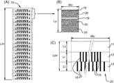
- リソグラフィ装置で使用するパターニングデバイスであって、
近接構造体を有する少なくとも1つの近接マークを備え、
前記近接構造体は、前記近接マークの長さ方向に沿って所定数隣接配置され、
前記各近接構造体は、前記近接マークの長さ方向に沿って順次隣接配置されたスペース構造体、基準構造体及び検査構造体を有し、
前記基準構造体には、前記近接マークの長さ方向に延在する線が前記近接マークの幅方向に沿って基準ピッチで第1の数だけ配置され、
前記検査構造体には、前記近接マークの長さ方向に延在する線が前記近接マークの幅方向に沿って検査ピッチで第2の数だけ配置される、
パターニングデバイス。 - 前記基準構造体の前記線が、前記リソグラフィ装置の限界寸法にほぼ等しい幅を有し、
前記限界寸法が、前記リソグラフィ装置によって前記基板へと転送される問題の構造体の最小寸法に対応する、
請求項1に記載のパターニングデバイス。 - 線の数と線の幅との積が、前記基準構造体と前記検査構造体との両方で同じである、
請求項1に記載のパターニングデバイス。 - 前記基準構造体の前記線が、前記リソグラフィ装置の限界寸法にほぼ等しい幅を有し、
前記限界寸法が、前記リソグラフィ装置によって前記基板へと転送される問題の構造体の最小寸法に対応し、
前記検査構造体の前記線の前記幅が、前記基準構造体の前記線の前記幅とほぼ等しく、
前記第1の数が前記第2の数と等しく、
前記基準ピッチが前記検査ピッチと等しくない、
請求項1に記載のパターニングデバイス。 - 線の数と線の幅との積が、前記基準構造体と前記検査構造体との両方で同じである、
請求項4に記載のパターニングデバイス。 - 前記基準構造体の前記線が、前記リソグラフィ装置の限界寸法とほぼ等しい幅を有し、
前記限界寸法が、前記リソグラフィ装置によって前記基板へと転送される問題の構造体の最小寸法に対応し、
前記検査構造体の前記線の前記幅が、前記基準構造体の前記線の前記幅の整数倍大きい、
請求項1に記載のパターニングデバイス。 - 線の数と線の幅との積が、前記基準構造体と前記検査構造体との両方で同じである、
請求項6に記載のパターニングデバイス。
Applications Claiming Priority (1)
| Application Number | Priority Date | Filing Date | Title |
|---|---|---|---|
| US11/317,244 US20070146670A1 (en) | 2005-12-27 | 2005-12-27 | Lithographic apparatus, patterning device and device manufacturing method |
Publications (2)
| Publication Number | Publication Date |
|---|---|
| JP2007180547A JP2007180547A (ja) | 2007-07-12 |
| JP4599343B2 true JP4599343B2 (ja) | 2010-12-15 |
Family
ID=38193244
Family Applications (1)
| Application Number | Title | Priority Date | Filing Date |
|---|---|---|---|
| JP2006342148A Expired - Fee Related JP4599343B2 (ja) | 2005-12-27 | 2006-12-20 | リソグラフィ装置、パターニングデバイスおよびデバイス製造方法 |
Country Status (2)
| Country | Link |
|---|---|
| US (1) | US20070146670A1 (ja) |
| JP (1) | JP4599343B2 (ja) |
Families Citing this family (4)
| Publication number | Priority date | Publication date | Assignee | Title |
|---|---|---|---|---|
| DE102006056625B4 (de) * | 2006-11-30 | 2014-11-20 | Globalfoundries Inc. | Verfahren und Teststruktur zum Bestimmen von Fokuseinstellungen in einem Lithographieprozess auf der Grundlage von CD-Messungen |
| EP2131243B1 (en) * | 2008-06-02 | 2015-07-01 | ASML Netherlands B.V. | Lithographic apparatus and method for calibrating a stage position |
| EP2458441B1 (en) * | 2010-11-30 | 2022-01-19 | ASML Netherlands BV | Measuring method, apparatus and substrate |
| EP3339957B1 (en) | 2016-12-20 | 2019-02-27 | GenISys GmbH | Process dose and process bias determination for beam lithography |
Citations (5)
| Publication number | Priority date | Publication date | Assignee | Title |
|---|---|---|---|---|
| JP2000012425A (ja) * | 1998-06-18 | 2000-01-14 | Toshiba Corp | 露光量測定方法と露光量測定用マスク |
| JP2001022051A (ja) * | 1999-07-09 | 2001-01-26 | Nec Corp | レチクル及び半導体装置の製造方法 |
| JP2002169266A (ja) * | 2000-11-30 | 2002-06-14 | Nikon Corp | マスク、結像特性計測方法、及び露光方法 |
| JP2003142385A (ja) * | 2001-11-06 | 2003-05-16 | Toshiba Corp | 露光装置の検査方法、焦点位置を補正する露光方法、および半導体装置の製造方法 |
| JP2004363313A (ja) * | 2003-06-04 | 2004-12-24 | Nikon Corp | 位置ずれ計測方法および装置、並びに位置ずれ計測用レチクル |
Family Cites Families (9)
| Publication number | Priority date | Publication date | Assignee | Title |
|---|---|---|---|---|
| JP3328676B2 (ja) * | 1991-11-28 | 2002-09-30 | 株式会社ニコン | 投影光学系の検査方法、マスク基板、及びマーク形成方法 |
| JP2803936B2 (ja) * | 1992-01-21 | 1998-09-24 | 三菱電機株式会社 | 投影露光装置及びパターン露光方法 |
| JP3309865B2 (ja) * | 1992-10-02 | 2002-07-29 | 株式会社ニコン | 結像特性計測方法及び該方法で使用されるマスク |
| DE69531854T2 (de) * | 1994-08-02 | 2004-08-19 | Koninklijke Philips Electronics N.V. | Verfahren zur wiederholten abbildung eines maskenmusters auf einem substrat |
| JPH10213895A (ja) * | 1997-01-30 | 1998-08-11 | Sony Corp | レチクルの合わせ測定用マーク |
| US6833221B2 (en) * | 2001-01-05 | 2004-12-21 | Litel Instruments | Method and apparatus for proper ordering of registration data |
| US6884552B2 (en) * | 2001-11-09 | 2005-04-26 | Kla-Tencor Technologies Corporation | Focus masking structures, focus patterns and measurements thereof |
| JP3884371B2 (ja) * | 2002-11-26 | 2007-02-21 | 株式会社東芝 | レチクル、露光モニタ方法、露光方法、及び半導体装置の製造方法 |
| SG108975A1 (en) * | 2003-07-11 | 2005-02-28 | Asml Netherlands Bv | Marker structure for alignment or overlay to correct pattern induced displacement, mask pattern for defining such a marker structure and lithographic projection apparatus using such a mask pattern |
-
2005
- 2005-12-27 US US11/317,244 patent/US20070146670A1/en not_active Abandoned
-
2006
- 2006-12-20 JP JP2006342148A patent/JP4599343B2/ja not_active Expired - Fee Related
Patent Citations (5)
| Publication number | Priority date | Publication date | Assignee | Title |
|---|---|---|---|---|
| JP2000012425A (ja) * | 1998-06-18 | 2000-01-14 | Toshiba Corp | 露光量測定方法と露光量測定用マスク |
| JP2001022051A (ja) * | 1999-07-09 | 2001-01-26 | Nec Corp | レチクル及び半導体装置の製造方法 |
| JP2002169266A (ja) * | 2000-11-30 | 2002-06-14 | Nikon Corp | マスク、結像特性計測方法、及び露光方法 |
| JP2003142385A (ja) * | 2001-11-06 | 2003-05-16 | Toshiba Corp | 露光装置の検査方法、焦点位置を補正する露光方法、および半導体装置の製造方法 |
| JP2004363313A (ja) * | 2003-06-04 | 2004-12-24 | Nikon Corp | 位置ずれ計測方法および装置、並びに位置ずれ計測用レチクル |
Also Published As
| Publication number | Publication date |
|---|---|
| US20070146670A1 (en) | 2007-06-28 |
| JP2007180547A (ja) | 2007-07-12 |
Similar Documents
| Publication | Publication Date | Title |
|---|---|---|
| JP5600145B2 (ja) | リソグラフィ装置のためのレベルセンサの構成及びデバイス製造方法 | |
| KR101066626B1 (ko) | 정렬 마크 제공 방법, 디바이스 제조 방법 및 리소그래피 장치 | |
| CN102171618B (zh) | 使用二维目标的光刻聚焦和剂量测量 | |
| JP5323875B2 (ja) | リソグラフィ装置及びデバイス製造方法 | |
| KR100985834B1 (ko) | 리소그래피 투영 장치의 포커스를 측정하는 방법 | |
| KR100825453B1 (ko) | 투영시스템의 배율측정방법, 디바이스 제조방법 및 컴퓨터프로그램물 | |
| JP4745292B2 (ja) | 波面センサを含むリソグラフィ装置 | |
| US7629697B2 (en) | Marker structure and method for controlling alignment of layers of a multi-layered substrate | |
| JP5312501B2 (ja) | アライメントマーク、基板、パターニングデバイスの組、およびデバイス製造方法 | |
| KR100803267B1 (ko) | 포커스 결정 방법, 디바이스 제조 방법, 및 마스크 | |
| JP4643627B2 (ja) | フォーカステスト実施方法およびデバイス製造方法 | |
| US7502097B2 (en) | Method and exposure apparatus for performing a tilted focus and a device manufactured accordingly | |
| JP4599343B2 (ja) | リソグラフィ装置、パターニングデバイスおよびデバイス製造方法 | |
| EP3379332A1 (en) | Lithographic apparatus being operable to determine pellicle degradation compensation corrections | |
| KR100832078B1 (ko) | 디바이스 제조방법 및 컴퓨터 프로그램 제품 | |
| JP4832493B2 (ja) | リソグラフィ方法及びデバイス製造方法 | |
| US7834975B2 (en) | Method and exposure apparatus for performing a tilted focus and a device manufactured accordingly | |
| JP2006210895A (ja) | 傾斜焦点試験を行う方法及び露光装置、並びにそれに応じて製造されたデバイス |
Legal Events
| Date | Code | Title | Description |
|---|---|---|---|
| A977 | Report on retrieval |
Free format text: JAPANESE INTERMEDIATE CODE: A971007 Effective date: 20091016 |
|
| A131 | Notification of reasons for refusal |
Free format text: JAPANESE INTERMEDIATE CODE: A131 Effective date: 20091020 |
|
| A521 | Written amendment |
Free format text: JAPANESE INTERMEDIATE CODE: A523 Effective date: 20100118 |
|
| TRDD | Decision of grant or rejection written | ||
| A01 | Written decision to grant a patent or to grant a registration (utility model) |
Free format text: JAPANESE INTERMEDIATE CODE: A01 Effective date: 20100831 |
|
| A01 | Written decision to grant a patent or to grant a registration (utility model) |
Free format text: JAPANESE INTERMEDIATE CODE: A01 |
|
| A61 | First payment of annual fees (during grant procedure) |
Free format text: JAPANESE INTERMEDIATE CODE: A61 Effective date: 20100927 |
|
| R150 | Certificate of patent or registration of utility model |
Free format text: JAPANESE INTERMEDIATE CODE: R150 |
|
| FPAY | Renewal fee payment (event date is renewal date of database) |
Free format text: PAYMENT UNTIL: 20131001 Year of fee payment: 3 |
|
| R250 | Receipt of annual fees |
Free format text: JAPANESE INTERMEDIATE CODE: R250 |
|
| R250 | Receipt of annual fees |
Free format text: JAPANESE INTERMEDIATE CODE: R250 |
|
| R250 | Receipt of annual fees |
Free format text: JAPANESE INTERMEDIATE CODE: R250 |
|
| R250 | Receipt of annual fees |
Free format text: JAPANESE INTERMEDIATE CODE: R250 |
|
| LAPS | Cancellation because of no payment of annual fees |