JP4599285B2 - Field effect transistor, integrated circuit, and memory - Google Patents
Field effect transistor, integrated circuit, and memory Download PDFInfo
- Publication number
- JP4599285B2 JP4599285B2 JP2005363624A JP2005363624A JP4599285B2 JP 4599285 B2 JP4599285 B2 JP 4599285B2 JP 2005363624 A JP2005363624 A JP 2005363624A JP 2005363624 A JP2005363624 A JP 2005363624A JP 4599285 B2 JP4599285 B2 JP 4599285B2
- Authority
- JP
- Japan
- Prior art keywords
- electrode
- field effect
- effect transistor
- magnetization
- source electrode
- Prior art date
- Legal status (The legal status is an assumption and is not a legal conclusion. Google has not performed a legal analysis and makes no representation as to the accuracy of the status listed.)
- Expired - Fee Related
Links
Images


Description
本発明は、電界効果トランジスタ、集積回路、及びメモリに係り、特に強磁性体を用いた電界効果トランジスタ、集積回路、及びメモリに関する。 The present invention relates to a field effect transistor, an integrated circuit, and a memory, and more particularly to a field effect transistor, an integrated circuit, and a memory using a ferromagnetic material.
電界効果トランジスタは1960年代に発明されて以来、飛躍的な性能の向上を遂げ、現在ではプロセッサやメモリーなどのLSIにとって最も重要なデバイスとなっている。その特徴は、フォトリソグラフィーにより大量生産が可能であり、プロセスの微細化により高集積化が可能である等の優れた性質を有する点であり、学術的・産業的に著しい進化を遂げてきた。 Field-effect transistors have improved dramatically since they were invented in the 1960s, and are now the most important devices for LSIs such as processors and memories. Its feature is that it has excellent properties such as mass production by photolithography and high integration by miniaturization of the process, and has made remarkable progress in academic and industrial fields.
特に、半導体プロセスの微細化における技術発展は激しく、プロセスルールはまもなく45 nm世代を迎えようとしている。しかしながら、この微細化に伴ってデバイスの物理長は著しく小さくなってきている。特に、ゲート絶縁膜の物理膜厚が薄くなりすぎる結果、ゲート-ソース電極間やゲート-ドレイン電極間のトンネル電流、いわゆるゲート・リーク電流が増大するとの深刻な問題を抱えている。このゲート・リーク電流は、130 nm世代や90 nm世代のLSIでは無視できるが、65 nm世代以降では何らかの対策を講じなければ、サブスレッショルド・リーク電流と同等以上の消費電力の増大を引き起こす(例えば、非特許文献1参照)。 In particular, technological developments in semiconductor process miniaturization are intense, and process rules are about to reach the 45 nm generation soon. However, along with this miniaturization, the physical length of the device has been remarkably reduced. In particular, there is a serious problem that a tunnel current between the gate and source electrodes or between the gate and drain electrodes, that is, a so-called gate leakage current increases as a result of the physical thickness of the gate insulating film becoming too thin. This gate leakage current is negligible in 130 nm and 90 nm generation LSIs, but if some measure is not taken after the 65 nm generation, it will cause an increase in power consumption equivalent to or greater than the subthreshold leakage current (for example, Non-Patent Document 1).
現在、ゲート・リーク電流の低減について、大きく分けて2つの方法が考えられている。1つはLSIの内部回路の電源電圧を制御する手法、もう1つは現行のSiO2よりも比誘電率が高い材料をゲート絶縁膜に用いる手法である。しかしながら、さらに低消費電力のトランジスタを作製するためには、前記の方法に加えてさらにリーク電流を低減することのできる手法が必要である。 At present, there are two broad methods for reducing gate leakage current. One is a method of controlling the power supply voltage of the internal circuit of the LSI, and the other is a method using a material having a relative dielectric constant higher than that of the current SiO 2 for the gate insulating film. However, in order to manufacture a transistor with lower power consumption, a method capable of further reducing the leakage current is required in addition to the above method.
また、近年では、電界効果トランジスタの一つの種類として、スピンを伝導に用いるスピン電界効果トランジスタが提案されている。これは、ソース電極またはドレイン電極に磁化を有する材質を用い、一方の磁化方向を可変にすることにより相互コンダクタンスを制御できるトランジスタであり、次世代のトランジスタとして期待されている(例えば、非特許文献2参照)。このスピン電界効果トランジスタを実用化する際にも、前述の電界効果トランジスタと同様のゲート・リーク電流問題が生じるため、何らかの対策が必要である。
以上説明したように、半導体プロセスが今後65 nm世代、45 nm世代とさらに微細化が進むに従い、電界効果トランジスタのゲート・リーク電流は急激に増大し、消費電力の増加を引き起こす。また、近年提案されているスピン電界効果トランジスタにおいても、同様のゲート・リーク電流の問題が生じる。 As described above, as the semiconductor process is further miniaturized in the 65 nm generation and the 45 nm generation in the future, the gate leakage current of the field effect transistor increases rapidly, causing an increase in power consumption. The same problem of gate leakage current also occurs in spin field effect transistors that have been recently proposed.
本発明はかかる実情に鑑みてなされたものであり、微細化が進んだ場合でもゲート・リーク電流の低減を図ることのできる電界効果トランジスタを実現することを目的とする。 The present invention has been made in view of such circumstances, and an object thereof is to realize a field effect transistor capable of reducing gate leakage current even when miniaturization is advanced.
上述した課題を解決するために、本発明の電界効果トランジスタは、磁化方向が
第1方向に固定された第1強磁性体電極と、磁化方向が前記第1方向と実質的に同じ方向
に固定された第2強磁性体電極と、前記第1強磁性体電極と前記第2強磁性体電極との間
のチャネルと、前記チャネル上にゲート絶縁層を介して設けられ磁化方向が前記第1方向
と実質的に反対の方向に固定された強磁性体層を備えたゲート電極とを具備することを特
徴とする。
In order to solve the above-described problems, a field effect transistor of the present invention includes a first ferromagnetic electrode whose magnetization direction is fixed in the first direction, and a magnetization direction fixed in substantially the same direction as the first direction. A second ferromagnetic electrode, a channel between the first ferromagnetic electrode and the second ferromagnetic electrode, and a magnetization direction provided on the channel via a gate insulating layer. And a gate electrode having a ferromagnetic layer fixed in a direction substantially opposite to the direction.
また、上述した本発明の電界効果トランジスタを備える集積回路を提供する。 Also provided is an integrated circuit comprising the field effect transistor of the present invention described above.
また、上述した本発明の電界効果トランジスタと記憶素子とをメモリセルに備えるメモリを提供する。 In addition, a memory provided with the above-described field effect transistor and memory element of the present invention in a memory cell is provided.
以上の本発明において、以下の構成を備えることが好ましい。 In the present invention described above, it is preferable to have the following configuration.
(1)前記第1強磁性体電極と前記チャネルとの間及び前記第2強磁性体電極と前記チ
ャネルとの間の少なくとも一方に設けられたトンネルバリア層を備えること。
( 1 ) A tunnel barrier layer is provided between at least one of the first ferromagnetic electrode and the channel and between the second ferromagnetic electrode and the channel.
(2)前記第1方向は、前記第1強磁性体電極と前記第2強磁性体電極とを結ぶ方向に
実質的に垂直な方向であること。
( 2 ) The first direction is a direction substantially perpendicular to a direction connecting the first ferromagnetic electrode and the second ferromagnetic electrode.
(3)前記第1方向は、前記第1強磁性体電極と前記第2強磁性体電極とを結ぶ方向に実質的に平行な方向であること。 ( 3 ) The first direction is a direction substantially parallel to a direction connecting the first ferromagnetic electrode and the second ferromagnetic electrode.
(4)前記ゲート電極は、前記ゲート絶縁層上に設けられた第1の強磁性体層と、この
第1の強磁性体層上に設けられた非磁性層と、この非磁性層上に設けられた第2の強磁性
体層とを備え、前記第1の強磁性体層の磁化方向が前記第1方向と実質的に反対の方向に
固定され、前記第2の強磁性体層の磁化方向が前記第1方向と実質的に同じ方向に固定さ
れていること。
( 4 ) The gate electrode includes a first ferromagnetic layer provided on the gate insulating layer, a nonmagnetic layer provided on the first ferromagnetic layer, and a nonmagnetic layer on the nonmagnetic layer. A second ferromagnetic layer provided, the magnetization direction of the first ferromagnetic layer being fixed in a direction substantially opposite to the first direction, The magnetization direction is fixed in substantially the same direction as the first direction.
(5)前記第1強磁性体電極、前記第2強磁性体電極、及び前記強磁性体層のうち少な
くとも一つの上に反強磁性層を備えること。
( 5 ) An antiferromagnetic layer is provided on at least one of the first ferromagnetic electrode, the second ferromagnetic electrode, and the ferromagnetic layer.
本発明によれば、微細化が進んだ場合でもゲート・リーク電流の低減を図ることのできる電界効果トランジスタを実現することが可能である。 According to the present invention, it is possible to realize a field effect transistor capable of reducing gate leakage current even when miniaturization is advanced.
以下、本発明の実施形態について図面を参照しつつ具体的に説明する。 Hereinafter, embodiments of the present invention will be specifically described with reference to the drawings.
(第1の実施形態)
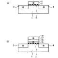
本実施形態は、ソース電極、ドレイン電極、ゲート電極のそれぞれの磁化方向が固定された電界効果トランジスタに関するものである。図1は、本実施形態に係る電界効果トランジスタの構造を示す断面図である。
(First embodiment)
This embodiment relates to a field effect transistor in which the magnetization directions of a source electrode, a drain electrode, and a gate electrode are fixed. FIG. 1 is a cross-sectional view showing the structure of the field effect transistor according to the present embodiment.
図1(a)に示すように、n型シリコン基板1の表面にソース電極3とドレイン電極4が埋め込み形成されている。ソース電極3とドレイン電極4はそれぞれ強磁性材料からなり、ソース電極3の磁化とドレイン電極4の磁化は互いに実質的に同じ方向(略平行な方向)に向いている。これらの磁化は、ソース電極3とドレイン電極4とを結ぶ方向(チャネル長さ方向)に実質的に垂直な方向を向いている。ソース電極3とドレイン電極4の間はチャネル領域2となるが、このチャネル領域2上にゲート絶縁膜5が形成されており、さらにゲート絶縁膜5上にはゲート電極6が形成されている。ゲート電極6も強磁性材料からなり、ゲート電極6の磁化はソース電極3やドレイン電極4の磁化に対して実質的に逆方向(略反平行な方向)に向いている。
As shown in FIG. 1A, a
この構造の電界効果トランジスタによれば、ソース電極3の磁化方向がゲート電極6の磁化方向と実質的に逆方向となっているので、ソース電極3とゲート電極6との間の抵抗がトンネル磁気抵抗効果により高くなり、両者の間にリーク電流が流れにくくなる。すなわち、ソース電極3とゲート電極6間のリーク電流は、MTJ(Magnetic Tunnel Junction、磁気トンネル接合)における磁化が略反平行状態のトンネル電流によって規定される。一般に、この相対的な磁化方向が略反平行の場合におけるトンネル電流は、磁化方向が略平行な場合や磁化を付与しない場合に比べて少なくなる。このため、ソース電極3とゲート電極6との間のリーク電流を低減することが可能である。
According to the field effect transistor having this structure, since the magnetization direction of the
このことは、ドレイン電極4とゲート電極6との間のリーク電流についても当てはまり、ドレイン電極4の磁化方向がゲート電極6の磁化方向と実質的に逆方向となっているので、ドレイン電極4とゲート電極6間にリーク電流が流れにくくなる。
This also applies to the leakage current between the
また、ソース電極3とゲート電極6間およびドレイン電極4とゲート電極6間には、チャネルを介したリーク電流も生じ得る。しかしながら、上記したようにソース電極3とゲート電極6間およびドレイン電極4とゲート電極6間の相対的な磁化方向を略反平行にとっておけば、磁気抵抗効果によりこのリーク電流も低減することが可能である。
In addition, a leak current can also occur between the
次に、図1(a)に示す電界効果トランジスタの製造方法について説明する。まず、n型シリコン基板1の表面にゲート絶縁膜5およびゲート電極6を形成する。次に、n型シリコン基板1においてソース電極3およびドレイン電極4が埋め込まれる部分をエッチングにより除去して凹部を形成する。次に、この凹部内に強磁性体膜を埋め込んで、ソース電極3およびドレイン電極4を形成する。さらに、ソース電極3、ドレイン電極4、ゲート電極6それぞれに対して磁化を付与する工程を行う。この工程は、一様磁場中にてアニールを行うプロセスを採用する。例えば、1Tの磁場中で300℃2時間のアニールを行えばよい。室温まで温度を下げた後に磁場を掃引すると、ソース電極・ドレイン電極とゲート電極の形状磁気異方性の違いにより、図1(a)に示す磁化配置を実現することができる。したがって、本製造方法においてはソース電極・ドレイン電極とゲート電極との形状が互いに異なるような設計が必要である。
Next, a method for manufacturing the field effect transistor shown in FIG. First, the
図1(b)は、本実施形態における変形例を示す図であり、ゲート絶縁膜15上に設けられるゲート電極を、強磁性体層16、非磁性体層17、強磁性体層18で構成する電界効果トランジスタの構造を示す。強磁性体層18の膜厚は強磁性体層16の膜厚よりも厚くなっており、強磁性体層16と強磁性体層18との間には反強磁性結合が生じている。強磁性体層18の磁化方向はソース電極3の磁化とドレイン電極4の磁化に対して実質的に同じ方向であり、磁性体層16の磁化方向はソース電極3の磁化とドレイン電極4の磁化に対して実質的に逆方向である。図1(b)の電界効果トランジスタにおいても、ソース電極3およびドレイン電極4の各々の磁化方向がゲート電極の強磁性体層16の磁化方向に対して実質的に逆方向となっているので、ソース電極3およびドレイン電極4とゲート電極6との間のリーク電流を低減することが可能である。
FIG. 1B is a diagram showing a modification of the present embodiment, and the gate electrode provided on the
次に、図1(b)に示す電界効果トランジスタの製造方法について説明する。まず、n型シリコン基板1の表面にゲート絶縁膜15、および強磁性体層16、非磁性体層17、強磁性体層18からなるゲート電極を形成する。次に、n型シリコン基板1においてソース電極3およびドレイン電極4が埋め込まれる部分をエッチングにより除去して凹部を形成する。次に、この凹部内に強磁性体膜を埋め込んで、ソース電極3およびドレイン電極4を形成する。さらに、ソース電極3、ドレイン電極4、ゲート電極それぞれに対して一様磁場中にてアニールを施すことにより、これらに磁化を付与する工程を行う。一様磁場中でアニールを行い、その後室温に戻すことにより、ソース電極3、ドレイン電極4、膜厚が厚い強磁性体層18の各々の磁化は互いに実質的に同じ方向を向くようになる。さらに、強磁性体層16と強磁性体層18間の反強磁性結合により、強磁性体層16の磁化方向はソース電極3、ドレイン電極4それぞれの磁化方向に対して実質的に逆方向となり、図1(b)の電界効果トランジスタを作製することができる。
Next, a method for manufacturing the field effect transistor shown in FIG. First, the gate electrode made of the
(第2の実施形態)
図2は本実施形態に係る電界効果トランジスタの構造を示す断面図である。図1と同一部分には同一符号を付して示す。本実施形態の電界効果トランジスタが第1の実施形態の電界効果トランジスタと異なる点は、ソース電極、ドレイン電極、ゲート電極それぞれの磁化の向きである。
(Second Embodiment)
FIG. 2 is a sectional view showing the structure of the field effect transistor according to the present embodiment. The same parts as those in FIG. 1 are denoted by the same reference numerals. The field effect transistor of this embodiment is different from the field effect transistor of the first embodiment in the magnetization directions of the source electrode, the drain electrode, and the gate electrode.
すなわち、図2(a)に示す電界効果トランジスタでは、ソース電極13、ドレイン電極14それぞれの磁化の向きは、ソース電極13とドレイン電極14とを結ぶ方向に実質的に平行な方向を向いている。ゲート絶縁膜25上に設けられたゲート電極26の磁化方向は、ソース電極13、ドレイン電極14それぞれの磁化方向に対して実質的に逆向きである。
That is, in the field effect transistor shown in FIG. 2A, the magnetization directions of the
また、図2(b)に示す電界効果トランジスタにおいても、図2(a)と同様であり、ゲート絶縁膜27上に強磁性体層28、非磁性体層29、強磁性体層30が積層して構成されたゲート電極において、強磁性体層28と強磁性体層30それぞれの磁化方向は、ソース電極13とドレイン電極14とを結ぶ方向に実質的に平行な方向を向いている。強磁性体層28と強磁性体層30間には反強磁性結合が存在し、強磁性体層28の磁化方向はソース電極13とドレイン電極14それぞれの磁化方向に対して実質的に逆向きである。
The field effect transistor shown in FIG. 2B is also the same as FIG. 2A, and the
図2(a)、(b)の電界効果トランジスタにおいても、第1の実施形態と同様にソース電極とゲート電極間のリーク電流、およびドレイン電極とゲート電極間のリーク電流を低減することが可能である。 In the field effect transistors of FIGS. 2A and 2B as well, the leakage current between the source electrode and the gate electrode and the leakage current between the drain electrode and the gate electrode can be reduced as in the first embodiment. It is.
(第3の実施形態)
図3は本実施形態に係る電界効果トランジスタの構造を示す断面図である。図1と同一部分には同一符号を付して示す。本実施形態の電界効果トランジスタが第1の実施形態の電界効果トランジスタと異なる点は、ソース電極、ドレイン電極、ゲート電極それぞれに反強磁性層が設けられていることである。
(Third embodiment)
FIG. 3 is a sectional view showing the structure of the field effect transistor according to the present embodiment. The same parts as those in FIG. 1 are denoted by the same reference numerals. The field effect transistor of this embodiment is different from the field effect transistor of the first embodiment in that an antiferromagnetic layer is provided on each of the source electrode, the drain electrode, and the gate electrode.
図3(a)に示すように、ソース電極3、ドレイン電極4、ゲート電極6それぞれの上には、反強磁性層31、反強磁性層32、反強磁性層33がそれぞれ形成されている。これらの反強磁性層31、32、33により、ソース電極3、ドレイン電極4、ゲート電極6それぞれの磁化安定性を得ることができる。
As shown in FIG. 3A, an
次に、図3(a)に示す電界効果トランジスタの製造方法について説明する。第1の実施形態と同様に、ゲート絶縁膜5、ゲート電極6、ソース電極3、およびドレイン電極4を形成した後、ソース電極3およびドレイン電極4上に反強磁性層31および反強磁性層32を、ゲート電極6上に反強磁性層33を形成する。反強磁性層31と反強磁性層32とは同じ材料から構成され、反強磁性層33はこれらの反強磁性層31、32のネール温度(T1)とは異なるネール温度を有する材料(T2)から構成される。
Next, a method for manufacturing the field effect transistor shown in FIG. Similar to the first embodiment, after forming the
次に、ソース電極3、ドレイン電極4、ゲート電極6それぞれに対して一様磁場中にてアニールを行うことにより、これらに磁化を付与する工程を行う。例えば、T1のネール温度がT2のネール温度よりも高い場合、反強磁性層T1のネール温度以上で一様磁場中においてアニールを行った後にT2のネール温度付近に降温し、磁場方向を180度回転してアニールを行い室温に戻せばよい。また、T2のネール温度がT1のネール温度よりも高い場合、反強磁性層T2のネール温度以上で一様磁場中においてアニールを行った後にT1のネール温度付近に降温し、磁場方向を180度回転してアニールを行い室温に戻せばよい。以上のアニール工程により、図3(a)の電界効果トランジスタを作製することができる。
Next, the
また、図3(b)に示す電界効果トランジスタにおいても、図3(a)と同様であり、ソース電極3、ドレイン電極4、ゲート電極の強磁性体層18それぞれの上には、反強磁性層31、反強磁性層32、反強磁性層33がそれぞれ形成されている。これらの反強磁性層31、32、33により、ソース電極3、ドレイン電極4、ゲート電極(強磁性体層16、18)それぞれの磁化安定性を得ることができる。なお、図3(b)の場合、反強磁性層31、反強磁性層32、反強磁性層33を同じ材料から構成することも可能である。
The field effect transistor shown in FIG. 3B is also the same as FIG. 3A, and an antiferromagnetic material is formed on each of the
図3(b)に示す電界効果トランジスタの製造方法は、図3(a)の電界効果トランジスタの製造方法とは異なり、第1の実施形態における図1(b)の電界効果トランジスタの製造方法を採用することができ、図3(a)の場合よりもより簡便に製造することが可能である。 The manufacturing method of the field effect transistor shown in FIG. 3B is different from the manufacturing method of the field effect transistor of FIG. 3A, and the manufacturing method of the field effect transistor of FIG. It can be employed and can be manufactured more simply than in the case of FIG.
(第4の実施形態)
本実施形態は、ソース電極、ゲート電極のそれぞれの磁化方向が固定され、ソース電極またはドレイン電極のいずれかの磁化方向が可変となっているスピン電界効果トランジスタに関するものである。図4、図5は、本実施形態に係るスピン電界効果トランジスタの構造を示す断面図である。
(Fourth embodiment)
The present embodiment relates to a spin field effect transistor in which the magnetization directions of the source electrode and the gate electrode are fixed and the magnetization direction of either the source electrode or the drain electrode is variable. 4 and 5 are cross-sectional views showing the structure of the spin field effect transistor according to the present embodiment.
まず、図4(a)に示すように、n型シリコン基板1の表面にソース電極43とドレイン電極44が埋め込み形成されている。ソース電極43とドレイン電極44はそれぞれ強磁性材料からなり、ソース電極43の磁化は、ソース電極43とドレイン電極44とを結ぶ方向に実質的に垂直な方向に固定されており、ドレイン電極44の磁化は可変となっている。ドレイン電極44の磁化は、ソース電極43の磁化と実質的に同じ方向か、或いは実質的に逆方向に向くよう構成されている。ソース電極43とドレイン電極44の間はチャネル領域2となるが、このチャネル領域2上にゲート絶縁膜5が形成されており、さらにゲート絶縁膜5上にはゲート電極6が形成されている。ゲート電極6も強磁性材料からなり、ゲート電極6の磁化はソース電極43の磁化に対して実質的に逆方向に向いている。
First, as shown in FIG. 4A, a
また、図5(a)のスピン電界効果トランジスタの場合は、図4(a)の場合とは逆にドレイン電極54の磁化は、ソース電極53とドレイン電極54とを結ぶ方向に実質的に垂直な方向に固定されており、ソース電極53の磁化は可変となっている。ソース電極53の磁化は、ドレイン電極54の磁化と実質的に同じ方向か、或いは実質的に逆方向に向くよう構成されている。
5A, the magnetization of the
次に、本実施形態に係るスピン電界効果トランジスタの動作機構について説明する。図4(a)に示したスピン電界効果トランジスタでは、ドレイン電極44の磁化が可変となっており、この磁化方向によってチャネル領域2に流れる電流を制御可能である。すなわち、ゲート電極6にしきい値電圧以上の電圧が印加されたとき、ドレイン電極44の磁化方向がソース電極43の磁化と逆向きの場合には、ソース電極43とドレイン電極44との間の抵抗がトンネル磁気抵抗効果により高くなってチャネル領域2には電流がほとんど流れない。一方、その逆にドレイン電極44の磁化方向がソース電極43の磁化と同じ向きの場合には、ソース電極43とドレイン電極44との間の抵抗がトンネル磁気抵抗効果により低くなってチャネル領域2には電流が流れる。図5(a)のスピン電界効果トランジスタにおいても、磁化が可変の電極がドレイン電極からソース電極へ入れ替わるだけであり、同様にチャネル領域2に流れる電流の制御が可能である。このようにチャネル領域2に流れる電流が制御可能であるので、ドレイン電極44やソース電極53の磁化方向を変化させることによりスピン電界効果トランジスタの出力電圧を制御することができ、プログラム可能な論理回路を組むことが可能となる。
Next, the operation mechanism of the spin field effect transistor according to this embodiment will be described. In the spin field effect transistor shown in FIG. 4A, the magnetization of the
図4(a)のスピン電界効果トランジスタによれば、第1の実施形態と同様に、ソース電極43の磁化方向がゲート電極6の磁化方向と実質的に逆方向となっているので、ソース電極43とゲート電極6との間の抵抗がトンネル磁気抵抗効果により高くなり、両者の間にリーク電流が流れにくくなる。
According to the spin field effect transistor of FIG. 4A, the magnetization direction of the
ここで、ドレイン電極44の磁化方向はゲート電極6の磁化方向に対して必ずしも逆方向とはならないので、リーク電流の問題が生じうる。したがって、図4(a)のスピン電界効果トランジスタは、ドレイン電極44側のリーク電流の問題を無視できる場合に効果的に適用することが可能である。より具体的に説明すると、トランジスタがオン状態の場合とオフ状態の場合とでリーク電流が生じる機構が異なり、トランジスタがオン状態のときはソース電極とゲート電極間のリーク電流が支配的であるのに対し、オフ状態のときはドレイン電極とゲート電極間のリーク電流が支配的である。このことを考慮すると、動作時にオン状態で使用される頻度が高いスピン電界効果トランジスタに対して、図4(a)のスピン電界効果トランジスタを効果的に適用することが可能である。
Here, since the magnetization direction of the
一方、図5(a)のスピン電界効果トランジスタによれば、第1の実施形態と同様に、ドレイン電極54の磁化方向がゲート電極6の磁化方向と実質的に逆方向となっているので、ドレイン電極54とゲート電極6との間の抵抗がトンネル磁気抵抗効果により高くなり、両者の間にリーク電流が流れにくくなる。ここで、ソース電極53の磁化方向はゲート電極6の磁化方向に対して必ずしも逆方向とはならないので、リーク電流の問題が生じうる。したがって、図5(a)のスピン電界効果トランジスタは、ソース電極53側のリーク電流の問題を無視できる場合に効果的に適用することが可能である。すなわち、上述したことを考慮すると、動作時にオフ状態で使用される頻度が高いスピン電界効果トランジスタに対して、図5(a)のスピン電界効果トランジスタを効果的に適用することが可能である。
On the other hand, according to the spin field effect transistor of FIG. 5A, the magnetization direction of the
図4(b)、図5(b)はそれぞれ、図4(a)、図5(a)に示すスピン電界効果トランジスタの変形例を示す図であり、それぞれゲート絶縁膜15上に設けられるゲート電極を、強磁性体層16、非磁性体層17、強磁性体層18で構成する電界効果トランジスタの構造を示す。強磁性体層18の膜厚は強磁性体層16の膜厚よりも厚くなっており、強磁性体層16と強磁性体層18との間には反強磁性結合が生じている。強磁性体層18の磁化方向はソース電極43の磁化やドレイン電極54の磁化に対して実質的に同じ方向であり、磁性体層16の磁化方向はソース電極43の磁化やドレイン電極54の磁化に対して実質的に逆方向である。図4(b)、図5(b)のスピン電界効果トランジスタにおいても、ソース電極43やドレイン電極54の各々の磁化方向がゲート電極の強磁性体層16の磁化方向に対して実質的に逆方向となっているので、それぞれソース電極43とゲート電極6との間、ドレイン電極54とゲート電極6との間のリーク電流を低減することが可能である。
FIGS. 4B and 5B are diagrams showing modifications of the spin field effect transistor shown in FIGS. 4A and 5A, respectively, and gates provided on the
図4、図5に示すスピン電界効果トランジスタの製造方法は、図1の電界効果トランジスタの製造方法と同様である。異なる点は、ソース電極とドレイン電極の強磁性体材料が異なる点である。磁化方向が可変となる電極には、磁化方向が固定される電極よりも反転磁界が小さな材料、もしくは反転磁界が小さな電極形状を用いる。 The manufacturing method of the spin field effect transistor shown in FIGS. 4 and 5 is the same as the manufacturing method of the field effect transistor of FIG. The difference is that the ferromagnetic materials of the source electrode and the drain electrode are different. For the electrode having a variable magnetization direction, a material having a smaller reversal magnetic field or an electrode shape having a smaller reversal magnetic field than an electrode having a fixed magnetization direction is used.
次に、本実施形態のスピン電界効果トランジスタにおいて、ソース電極やドレイン電極の磁化方向を変化させるための構造について説明する。図6はこの構造を示す断面図である。ここでは、ソース電極53の磁化方向を変化させる場合を一例として説明する。ドレイン電極の磁化方向を変化させる場合も同様である。
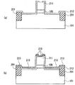
Next, a structure for changing the magnetization direction of the source electrode and the drain electrode in the spin field effect transistor of this embodiment will be described. FIG. 6 is a sectional view showing this structure. Here, a case where the magnetization direction of the
図6(a)に示すようにソース電極53やドレイン電極54が埋め込まれる半導体層64と支持基板61との間には、書込み配線62と、書込み配線62と半導体層64間を絶縁する絶縁層63とが設けられる。書込み配線62には電流が流れ、この電流により矢印方向に発生する磁場により半導体ソース電極53の磁化方向を変化させることができる。すなわち、当該電流の流れる向きを変えることにより、発生する磁場の方向も変化し、これに基づいてソース電極53の磁化方向を変化させて書込みを行うことができる。
As shown in FIG. 6A, between the
図6(b)は変形例であり、スピン電界効果トランジスタの上に書込み配線67を設ける例である。スピン電界効果トランジスタと書込み配線67との間にはこれらを絶縁する絶縁層66が設けられている。この変形例においても、書込み配線67に流れる電流の向きを変えることにより、発生する磁場の方向(矢印方向)も変化し、これに基づいてソース電極53の磁化方向を変化させて書込みを行うことができる。
FIG. 6B shows a modified example in which the
(第5の実施形態)
図7、図8は本実施形態に係るスピン電界効果トランジスタの構造を示す断面図である。図4、図5と同一部分には同一符号を付して示す。本実施形態のスピン電界効果トランジスタが第4の実施形態のスピン電界効果トランジスタと異なる点は、ソース電極、ドレイン電極、ゲート電極に反強磁性層が設けられていることである。
(Fifth embodiment)
7 and 8 are cross-sectional views showing the structure of the spin field effect transistor according to the present embodiment. The same parts as those in FIGS. 4 and 5 are denoted by the same reference numerals. The spin field effect transistor of this embodiment is different from the spin field effect transistor of the fourth embodiment in that an antiferromagnetic layer is provided on the source electrode, the drain electrode, and the gate electrode.
図7(a)に示すように、ソース電極43、ゲート電極6それぞれの上には、反強磁性層71、反強磁性層72がそれぞれ形成されている。これらの反強磁性層71、72により、ソース電極43、ゲート電極6それぞれの磁化安定性を得ることができる。また、図7(b)では、ゲート電極6、ドレイン電極54それぞれの上には、反強磁性層72、反強磁性層73がそれぞれ形成されている。これらの反強磁性層72、73により、ゲート電極6、ドレイン電極54それぞれの磁化安定性を得ることができる。
As shown in FIG. 7A, an
さらに、図8(a)に示すように、ソース電極43、ゲート電極の強磁性体層18それぞれの上には、反強磁性層71、反強磁性層72がそれぞれ形成され、図8(b)に示すように、ゲート電極の強磁性体層18、ドレイン電極54それぞれの上には、反強磁性層72、反強磁性層73がそれぞれ形成されている。これらの反強磁性層71、72、73によっても、ソース電極43、ゲート電極、ドレイン電極54それぞれの磁化安定性を得ることができる。
Further, as shown in FIG. 8A, an
また、これらの反強磁性層71、72、73を用いることにより、スピン電界効果トランジスタの製造方法も簡便なものとなる。すなわち、ソース電極43、ゲート電極の強磁性体層18、ドレイン電極44を同じ強磁性体材料により形成した場合でも、反強磁性層71、72をそれぞれソース電極43、強磁性体層18の上に形成し、ドレイン電極44の上には反強磁性層を形成しないプロセスとするだけで、ソース電極43、強磁性体層18それぞれの磁化方向を固定するとともにドレイン電極44の磁化方向を可変とする構造を簡便に製造することができる。
In addition, by using these
(第6の実施形態)
本実施形態は、第1の実施形態の図1の電界効果トランジスタにおいてソース電極とチャネルとの間及びドレイン電極とチャネルとの間にトンネルバリア層を設けたものである。図9は、本実施形態に係る電界効果トランジスタの構造を示す断面図である。
(Sixth embodiment)
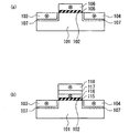
In the present embodiment, tunnel barrier layers are provided between the source electrode and the channel and between the drain electrode and the channel in the field effect transistor of FIG. 1 of the first embodiment. FIG. 9 is a cross-sectional view showing the structure of the field effect transistor according to the present embodiment.
図9(a)に示すように、n型シリコン基板101の表面にソース電極103とドレイン電極104が埋め込み形成されている。n型シリコン基板101の表面とソース電極103との間、及びn型シリコン基板101の表面とドレイン電極104との間にそれぞれトンネルバリア膜107が形成されている。ソース電極103とドレイン電極104はそれぞれ強磁性材料からなり、ソース電極103とドレイン電極104の磁化は、ソース電極103とドレイン電極104とを結ぶ方向に実質的に垂直な方向に固定されている。ソース電極103とドレイン電極104の間はチャネル領域102となるが、このチャネル領域102上にゲート絶縁膜5が形成されており、さらにゲート絶縁膜5上にはゲート電極106が形成されている。ゲート電極106も強磁性材料からなり、ゲート電極106の磁化はソース電極103、ドレイン電極104の磁化に対して実質的に逆方向に向いている。
As shown in FIG. 9A, the
本実施形態の電界効果トランジスタによれば、トンネルバリア膜107が、n型シリコン基板101の表面とソース電極103との間で生じうる反応や、n型シリコン基板101の表面とドレイン電極104との間で生じうる反応をそれぞれ防止する役割を果たす。すなわち、製造過程でトランジスタが高温に晒されると、上述した反応が生ずる場合があるが、本実施形態によればこのような反応を抑制することができる。したがって、ソース電極103、ドレイン電極104とn型シリコン基板101の表面との間の接合を良好に形成することができ、トランジスタの製造歩留まりを向上させることが可能である。
According to the field effect transistor of the present embodiment, the
なお、求められるトランジスタの性能等に応じて、n型シリコン基板101の表面とソース電極103との間、及びn型シリコン基板101の表面とドレイン電極104との間のうち片方のみにトンネルバリア膜を形成する構造を採用することも可能である。
Note that a tunnel barrier film is formed only on one of the surface of the n-
図9(b)は、本実施形態における変形例を示す図であり、ゲート絶縁膜115上に設けられるゲート電極を、強磁性体層116、非磁性体層117、強磁性体層118で構成する電界効果トランジスタの構造を示す。強磁性体層118の膜厚は強磁性体層116の膜厚よりも厚くなっており、強磁性体層116と強磁性体層118との間には反強磁性結合が生じている。強磁性体層118の磁化方向はソース電極103の磁化とドレイン電極104の磁化に対して実質的に同じ方向であり、磁性体層116の磁化方向はソース電極103の磁化とドレイン電極104の磁化に対して実質的に逆方向である。この構造によっても図9(a)と同様の効果を得ることができる。
FIG. 9B is a diagram showing a modification of the present embodiment, and the gate electrode provided on the
(第7の実施形態)
本実施形態は、第5の実施形態の図7、図8のスピン電界効果トランジスタにおいてソース電極とチャネルとの間及びドレイン電極とチャネルとの間にトンネルバリア層を設けたものである。図10及び図11は、本実施形態に係るスピン電界効果トランジスタの構造を示す断面図である。
(Seventh embodiment)
In this embodiment, a tunnel barrier layer is provided between the source electrode and the channel and between the drain electrode and the channel in the spin field effect transistor of FIGS. 7 and 8 of the fifth embodiment. 10 and 11 are cross-sectional views showing the structure of the spin field effect transistor according to this embodiment.
図10(a)に示すように、n型シリコン基板101の表面にソース電極143とドレイン電極144が埋め込み形成されている。n型シリコン基板101の表面とソース電極143との間、及びn型シリコン基板101の表面とドレイン電極144との間にそれぞれトンネルバリア膜107が形成されている。ソース電極143とドレイン電極144はそれぞれ強磁性材料からなり、ソース電極143の磁化は、ソース電極143とドレイン電極144とを結ぶ方向に実質的に垂直な方向に固定されており、ドレイン電極144の磁化は可変となっている。ドレイン電極144の磁化は、ソース電極143の磁化と実質的に同じ方向か、或いは実質的に逆方向に向くよう構成されている。ソース電極143とドレイン電極144の間はチャネル領域102となるが、このチャネル領域102上にゲート絶縁膜105が形成されており、さらにゲート絶縁膜105上にはゲート電極106が形成されている。ゲート電極106も強磁性材料からなり、ゲート電極106の磁化はソース電極143の磁化に対して実質的に逆方向に向いている。また、ソース電極143、ゲート電極106それぞれの上には、反強磁性層171、反強磁性層172がそれぞれ形成されている。これらの反強磁性層171、172によって、ソース電極143、ゲート電極106それぞれの磁化安定性を得ることができる。
As shown in FIG. 10A, a
また、図10(b)のスピン電界効果トランジスタの場合も、n型シリコン基板101の表面とソース電極153との間、及びn型シリコン基板101の表面とドレイン電極154との間にそれぞれトンネルバリア膜107が形成されている。図10(b)のスピン電界効果トランジスタでは、図10(a)の場合とは逆にドレイン電極154の磁化は、ソース電極153とドレイン電極154とを結ぶ方向に実質的に垂直な方向に固定されており、ソース電極153の磁化は可変となっている。ソース電極153の磁化は、ドレイン電極154の磁化と実質的に同じ方向か、或いは実質的に逆方向に向くよう構成されている。また、ゲート電極106、ドレイン電極154それぞれの上には、反強磁性層172、反強磁性層173がそれぞれ形成されている。これらの反強磁性層172、173によって、ゲート電極106、ドレイン電極154それぞれの磁化安定性を得ることができる。
Also in the case of the spin field effect transistor of FIG. 10B, tunnel barriers are provided between the surface of the n-
図11(a)、(b)はそれぞれ、図10(a)、(b)の変形例を示す図であり、ゲート絶縁膜115上に設けられるゲート電極を、強磁性体層116、非磁性体層117、強磁性体層118で構成するスピン電界効果トランジスタの構造を示す。強磁性体層118の膜厚は強磁性体層116の膜厚よりも厚くなっており、強磁性体層116と強磁性体層118との間には反強磁性結合が生じている。強磁性体層118の磁化方向はソース電極143の磁化やドレイン電極154の磁化に対して実質的に同じ方向であり、磁性体層116の磁化方向はソース電極143の磁化やドレイン電極154の磁化に対して実質的に逆方向である。強磁性体層118の上には反強磁性層172が設けられ、ゲート電極の磁化安定性を得ることができる。
FIGS. 11A and 11B are diagrams showing modifications of FIGS. 10A and 10B, respectively. The gate electrode provided on the
本実施形態のスピン電界効果トランジスタによれば、トンネルバリア膜107が、n型シリコン基板101の表面とソース電極143、153との間で生じうる反応や、n型シリコン基板101の表面とドレイン電極144、154との間で生じうる反応をそれぞれ防止する役割を果たす。したがって、ソース電極143、153とn型シリコン基板101の表面との間の接合、ドレイン電極144、154とn型シリコン基板101の表面との間の接合を良好に形成することができ、トランジスタの製造歩留まりを向上させることが可能である。
According to the spin field effect transistor of this embodiment, the
さらに、トンネルバリア膜を付与したことで、チャネル領域102に高スピン偏極率でキャリアを注入できる。したがって、ソース電極153やドレイン電極144の磁化方向の変化に伴う相互コンダクタンスの変化を大きくとることができる。
Further, by providing the tunnel barrier film, carriers can be injected into the
なお、求められるトランジスタの性能等に応じて、n型シリコン基板101の表面とソース電極143、153との間、及びn型シリコン基板101の表面とドレイン電極144、154との間のうち片方のみにトンネルバリア膜を形成する構造を採用することも可能である。また、必要に応じて、図4、図5のように反強磁性層を省略することもできる。
Note that only one of the surface between the surface of the n-
上述した第1〜第7の実施形態において、以下の材料を採用することができる。 In the first to seventh embodiments described above, the following materials can be employed.
まず、上記実施形態において、n型シリコン基板の代わりにp型シリコン基板を用いることができ、さらに、Ge、SixGe1−x(0<x<1)や、III−V族やII−VI族の化合物半導体などを用いることもできる。 First, in the above-described embodiment, a p-type silicon substrate can be used instead of an n-type silicon substrate. Further, Ge, Si x Ge 1-x (0 <x <1), III-V group, II- A group VI compound semiconductor can also be used.
また、反強磁性層としては、Fe-Mn(鉄−マンガン)、Pt-Mn(白金−マンガン)、Pt-Cr-Mn(白金−クロム−マンガン)、Ni-Mn(ニッケル−マンガン)、Ir-Mn(イリジウム−マンガン)、NiO(酸化ニッケル)、Fe2O3(酸化鉄)などを用いることができる。 Antiferromagnetic layers include Fe-Mn (iron-manganese), Pt-Mn (platinum-manganese), Pt-Cr-Mn (platinum-chromium-manganese), Ni-Mn (nickel-manganese), Ir -Mn (iridium-manganese), NiO (nickel oxide), Fe 2 O 3 (iron oxide), or the like can be used.
また、強磁性体からなるソース電極、ドレイン電極、ゲート電極の各電極は一方向異方性を有することが望ましい。その膜厚は0.1 nmから100 nmが好ましい。さらに、これらの電極の膜厚は、超常磁性にならない程度の厚さが必要であり、0.4 nm以上であることがより望ましい。その材料は、Co、Fe、Niまたはそれらの合金、Co-Pt、Co-Fe-Pt、Fe-Pt、Co-Fe-Cr-Pt、C0-Cr-Ptや、CrO2、Co2MnGe、Co2MnAl、Co2MnSi、CoCrFeAlなどのホイスラー合金やハーフメタル材料、SiMn、GeMnなどの磁性半導体からなる群より選ばれる少なくとも1種を用いることが好ましい。なお、上記磁性材料に、Ag(銀)、Cu(銅)、Au(金)、Al(アルミニウム)、Ru(ルテニウム)、Os(オスニウム)、Re(レニウム)、Ta(タンタル)、B(ボロン)、C(炭素)、O(酸素)、N(窒素)、Pd(パラジウム)、Pt(白金)、Zr(ジルコニウム)、Ir(イリジウム)、W(タングステン)、Mo(モリブデン)、Nb(ニオブ)などの非磁性元素を添加して、磁気特性を調節したり、結晶性、機械的特性、化学的特性などの各種物性を調節することができる。 Further, it is desirable that each of the source electrode, the drain electrode, and the gate electrode made of a ferromagnetic material has unidirectional anisotropy. The film thickness is preferably from 0.1 nm to 100 nm. Furthermore, the film thickness of these electrodes needs to be a thickness that does not become superparamagnetic, and is more preferably 0.4 nm or more. The materials are Co, Fe, Ni or their alloys, Co-Pt, Co-Fe-Pt, Fe-Pt, Co-Fe-Cr-Pt, C0-Cr-Pt, CrO 2, Co 2 MnGe, It is preferable to use at least one selected from the group consisting of Heusler alloys such as Co 2 MnAl, Co 2 MnSi, and CoCrFeAl, half-metal materials, and magnetic semiconductors such as SiMn and GeMn. In addition, Ag (silver), Cu (copper), Au (gold), Al (aluminum), Ru (ruthenium), Os (osnium), Re (rhenium), Ta (tantalum), B (boron) ), C (carbon), O (oxygen), N (nitrogen), Pd (palladium), Pt (platinum), Zr (zirconium), Ir (iridium), W (tungsten), Mo (molybdenum), Nb (niobium) ) And other nonmagnetic elements can be added to adjust the magnetic properties and various physical properties such as crystallinity, mechanical properties, and chemical properties.
また、ゲート電極において強磁性体層に挟まれる非磁性体層の材料としては、Ru、Re、Irなどを用いることができる。 Further, Ru, Re, Ir, or the like can be used as a material of the nonmagnetic layer sandwiched between the ferromagnetic layers in the gate electrode.
さらにまた、トンネルバリア層としては、Si、Ge、Al、Ga、Mg、Ti等の酸化物または窒化物を用いることができる。 Furthermore, as the tunnel barrier layer, oxides or nitrides such as Si, Ge, Al, Ga, Mg, and Ti can be used.
次に、本発明の実施例について図面を用いつつ詳細に説明する。 Next, embodiments of the present invention will be described in detail with reference to the drawings.
(実施例1)
本実施例として、図3(b)に示す構造を有する電界効果トランジスタを作製した。その作製手順は、ソース電極3、ドレイン電極4の部分等を除き通常のSiプロセスとほぼ同様であるが、製造プロセスに沿って説明する。図14は実施例1の製造プロセスを示す工程断面図である。
Example 1
As this example, a field effect transistor having the structure shown in FIG. The manufacturing procedure is substantially the same as the normal Si process except for the
まず、n型シリコン基板1上にシリコン酸化膜(SiOx膜)を形成し、さらにこの上にシランとアンモニアを用いてシリコン窒化膜(Si3N4膜)を気相成長した。さらに、PEPを行い、ソース電極3、ゲート酸化膜15、ドレイン電極4となる部分の上に選択的にフォトレジストを形成する。次に、このフォトレジストをマスクとしてSi3N4膜をエッチングし、さらにSi3N4膜をマスクとしてその下のSiOx膜、n型シリコン基板1表面をエッチング除去する。
First, a silicon oxide film (SiO x film) was formed on the n-
その後、エッチング除去により露出したn型シリコン基板1の領域上に厚い素子分離用フィールドシリコン酸化膜201を形成する。さらに、ソース電極3、ゲート酸化膜15、ドレイン電極4となる部分の上に残っているSi3N4膜をリン酸で除去し、その下のSiOx膜もフッ酸で除去する。
Thereafter, a thick element isolation field
次に、熱酸化法によりゲート絶縁膜15としてシリコン酸化膜(SiOx膜)を15 nmの膜厚で成長させ、続いてこのゲート絶縁膜15上に(Co70Fe30)80B20(5 nm)16/Ru(0.95 nm)17/ Co70Fe30(5 nm)18/PtMn(15 nm)33/Ta(300 nm)を堆積した(括弧内は膜厚。)。この後、これらの積層膜に対してフォトリソグラフィーやエッチングを施して、ゲート電極パターン202を形成した。
Next, a silicon oxide film (SiO x film) is grown to a thickness of 15 nm as the
次に、このゲート電極パターン202をマスクとして、フッ素系ガスを用いたRIE(反応性イオンエッチング)により、ゲート絶縁膜15、並びにソース電極3、ドレイン電極4となる部分のn型シリコン基板1の表面領域を除去し、図14(a)の構造を作製した。その後、図14(b)に示すように、このエッチング除去部分にソース電極3及びドレイン電極4として、(Co70Fe30)80B20(5 nm)/Ta(300 nm)の積層膜203を堆積した。さらに、反強磁性層31、32としてPtMn(15 nm)膜204を堆積した。積層膜203やPtMn膜204の堆積には、指向性の強いスパッタ装置によるスパッタを用いると良い。
Next, by using the
その後、必要に応じて、素子分離用フィールドシリコン酸化膜201やゲート電極パターン202の上に残った積層膜203やPtMn膜204を除去し、層間絶縁膜やコンタクトホールを形成し、測定電極となるアルミ配線を形成した。最後に、一様磁場中でアニールを行った。磁場の大きさは8000 Oeとした。この磁場中アニールにより、ソース電極3、ドレイン電極4、膜厚が厚い強磁性体層18の各々の磁化は互いに実質的に同じ方向を向くようになった。さらに、強磁性体層16と強磁性体層18間の反強磁性結合により、強磁性体層16の磁化方向はソース電極3、ドレイン電極4それぞれの磁化方向に対して実質的に逆方向となり、図1(b)の電界効果トランジスタを作製することができた。
Thereafter, if necessary, the
また、比較例としてゲート電極、ソース電極、およびドレイン電極に非磁性材料であるAl-Siを用いたトランジスタを作製した。 As a comparative example, a transistor using Al—Si, which is a nonmagnetic material, was manufactured for the gate electrode, the source electrode, and the drain electrode.
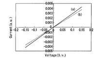
このようにして作製した本実施例のトランジスタと比較例のトランジスタに対して、リーク電流の測定を行った。測定手順は次の通りである。まず、非磁性材料からなる電極を有する比較例のトランジスタのソース電極をグランドに接続し、ゲート電極に正電圧+VGを印加し、ゲート電極とソース電極間に流れる電流を測定したところ、図12(a)に示されるI−V特性を得た。 The leakage current was measured for the transistor of this example and the transistor of the comparative example manufactured as described above. The measurement procedure is as follows. First, the source electrode of a comparative transistor having an electrode made of a nonmagnetic material was connected to the ground, a positive voltage + VG was applied to the gate electrode, and the current flowing between the gate electrode and the source electrode was measured. The IV characteristics shown in a) were obtained.
次に、強磁性体材料からなる電極を有する本実施例のトランジスタのソース電極3をグランドに接続し、ゲート電極に正電圧+VGを印加し、ゲート電極とソース電極間に流れる電流を測定したところ、図12(b)に示されるI−V特性を得た。
Next, the
図12に示されるように、比較例のトランジスタの場合(図12(a))に比べて、本実施例のトランジスタの場合(図12(b))には、約17%の電流が削減される。したがって、本実施例の構造を用いることによりリーク電流を低減させることが可能であることがわかる。また、本実施例のトランジスタにおいてソース電極3とドレイン電極4とは可換な構造を有しているため、上記の結果から、本実施例の構造はゲート電極とドレイン電極間のリーク電流低減にも効果があると考えられる。
As shown in FIG. 12, in the case of the transistor of this example (FIG. 12B), the current of about 17% is reduced compared to the case of the transistor of the comparative example (FIG. 12A). The Therefore, it can be seen that leakage current can be reduced by using the structure of this embodiment. In addition, since the
(実施例2)
本実施例として、図11(a)に示す構造を有するスピン電界効果トランジスタを作製した。その作製手順は、トンネルバリア層を形成する点を除き実施例1のプロセスとほぼ同様であるが、製造プロセスに沿って説明する。図15は実施例2の製造プロセスを示す工程断面図である。
(Example 2)
As this example, a spin field effect transistor having the structure shown in FIG. The manufacturing procedure is substantially the same as the process of the first embodiment except that the tunnel barrier layer is formed, but will be described along the manufacturing process. FIG. 15 is a process cross-sectional view illustrating the manufacturing process of the second embodiment.
実施例1の図14(a)に示す構造を作製した後、極薄(例えば、(1 nm))のMgO膜をスパッタ法により堆積し、スパッタ堆積された膜をプラズマ酸化することによりトンネルバリア層107を作製した。Mg膜をスパッタ堆積した後に、スパッタ堆積された膜をプラズマ酸化してもよい。その後、実施例1の製造工程と同様に、ソース電極143及びドレイン電極144として、(Co70Fe30)80B20(5 nm)/Ta(300 nm)の積層膜213を堆積した。MgOスパッタ、プラズマ酸化、積層膜213の堆積の各工程は、真空を破らず連続的に行われることが好ましい。さらに、ドレイン電極144上にレジストマスクを設け、反強磁性層171としてPtMn(15 nm)膜をソース電極143上にのみ形成した。その後、実施例1と同様の製造工程により、本実施例のスピン電界効果トランジスタを作製した。本実施例のスピン電界効果トランジスタは、強磁性体層116と強磁性体層118との間には反強磁性結合が生じており、強磁性体層118の磁化方向はソース電極143の磁化に対して実質的に同じ方向であり、磁性体層116の磁化方向はソース電極143の磁化に対して実質的に逆方向であった。ドレイン電極144の磁化方向は、ソース電極143の磁化に対して実質的に同じか或いは逆の方向に可変となった。なお、ソース電極143及びドレイン電極144の作製は、ドレイン部、ソース部を片方ずつレジストマスクで覆って各電極の作製プロセスを行っても良い。
After the structure shown in FIG. 14A of Example 1 is fabricated, a tunnel barrier is formed by depositing an extremely thin (for example, (1 nm)) MgO film by sputtering and plasma oxidizing the sputtered film.
また、比較例として、磁性体層116に相当する層の磁化方向がソース電極の磁化に対して実質的に同じ方向となる以外は本実施例の構造と同じであるトランジスタを作製した。
Further, as a comparative example, a transistor having the same structure as that of this example except that the magnetization direction of the layer corresponding to the
このようにして作製した本実施例のトランジスタと比較例のトランジスタに対して、リーク電流の測定を行った。測定手順は次の通りである。まず、比較例のトランジスタのソース電極をグランドに接続し、ゲート電極に正電圧+VGを印加し、ゲート電極とソース電極間に流れる電流を測定したところ、図13(a)に示されるI−V特性を得た。 The leakage current was measured for the transistor of this example and the transistor of the comparative example manufactured as described above. The measurement procedure is as follows. First, when the source electrode of the transistor of the comparative example was connected to the ground, a positive voltage + VG was applied to the gate electrode, and the current flowing between the gate electrode and the source electrode was measured, the IV shown in FIG. Got the characteristics.
次に、ドレイン電極の磁化方向を固定するために100 Oeの磁場を印加しながら、本実施例のトランジスタのソース電極143をグランドに接続し、ゲート電極に正電圧+VGを印加し、ゲート電極とソース電極間に流れる電流を測定したところ、図13(b)に示されるI−V特性を得た。
Next, while applying a magnetic field of 100 Oe to fix the magnetization direction of the drain electrode, the
図13に示されるように、比較例のトランジスタの場合(図13(a))に比べて、本実施例のトランジスタの場合(図13(b))には、約13%の電流が削減される。したがって、本実施例の構造を用いることによりリーク電流を低減させることが可能であることがわかる。また、本実施例のトランジスタにおいてソース電極3とドレイン電極4とは可換な構造を有しているため、上記の結果から、本実施例の構造はゲート電極とドレイン電極間のリーク電流低減にも効果があると考えられる。
As shown in FIG. 13, in the case of the transistor of this example (FIG. 13B), the current of about 13% is reduced compared to the case of the transistor of the comparative example (FIG. 13A). The Therefore, it can be seen that leakage current can be reduced by using the structure of this embodiment. In addition, since the
なお、本発明は上記実施形態、実施例に限定されることは無い。例えば、チャネルの型としてはエンハンス型に限らずデプリーション型のものを用いることができる。チャネルの製造方法としては、イオン注入のみならず、変調ドープを用いたヘテロ界面成長プロセスにより作製してもよい。 In addition, this invention is not limited to the said embodiment and Example. For example, the channel type is not limited to the enhancement type, and a depletion type can be used. As a channel manufacturing method, not only ion implantation but also a heterointerface growth process using modulation doping may be used.
また、上記実施形態、実施例の電界効果トランジスタを用いて集積回路を構成してもよい。上記実施形態、実施例の電界効果トランジスタと記憶素子とをメモリセルに備えるメモリを構成してもよい。例えば、誘電体キャパシタと組み合わせればDRAM(Dynamic Random Access Memory)を、強誘電体キャパシタと組み合わせればFRAM(Ferroelectric Random Access Memory)を、磁気抵抗効果素子と組み合わせればMRAM(Magnetic Random Access Memory)を構成することができる。さらにまた、EEPROM(データの書込みや消去を電気的に行うプログラム可能なリード・オンリ・メモリ)のトランジスタにも上記実施形態、実施例の電界効果トランジスタを適用することが可能である。 In addition, an integrated circuit may be configured using the field effect transistors of the above-described embodiments and examples. You may comprise the memory which equips a memory cell with the field effect transistor and memory element of the said embodiment and an Example. For example, DRAM (Dynamic Random Access Memory) when combined with a dielectric capacitor, FRAM (Ferroelectric Random Access Memory) when combined with a ferroelectric capacitor, and MRAM (Magnetic Random Access Memory) when combined with a magnetoresistive element. Can be configured. Furthermore, the field effect transistors of the above embodiments and examples can be applied to the transistors of EEPROM (programmable read-only memory for electrically writing and erasing data).
さらにまた、上記実施形態、実施例のスピン電界効果トランジスタの磁化可変電極(ソース電極またはドレイン電極)を記憶部として用い、データを当該電極の磁化方向として記憶し、ソース電極とドレイン電極間に生ずる磁気抵抗効果を利用して当該データを読み出すメモリを提供することもできる。 Furthermore, the magnetization variable electrode (source electrode or drain electrode) of the spin field effect transistor of the above embodiment or example is used as a storage unit, and data is stored as the magnetization direction of the electrode, and is generated between the source electrode and the drain electrode. It is also possible to provide a memory that reads out the data using the magnetoresistive effect.
その他、本発明は上記実施形態や実施例そのままに限定されるものではなく、実施段階ではその要旨を逸脱しない範囲で構成要素を変形して具体化できる。また、上記実施形態や実施例に開示されている複数の構成要素の適宜な組み合わせにより、種々の発明を形成できる。例えば、実施形態や実施例に示される全構成要素から幾つかの構成要素を削除してもよい。さらに、異なる実施形態や実施例にわたる構成要素を適宜組み合わせてもよい。 In addition, the present invention is not limited to the above-described embodiments and examples as they are, and can be embodied by modifying constituent elements without departing from the scope of the invention in the implementation stage. Moreover, various inventions can be formed by appropriately combining a plurality of constituent elements disclosed in the above-described embodiments and examples. For example, you may delete some components from all the components shown by embodiment and an Example. Furthermore, you may combine suitably the component covering different embodiment and an Example.
1、101…n型シリコン基板
2、102…チャネル領域
3、43、53、103、143、153…ソース電極
4、44、54、104、144、154…ドレイン電極
5、15、25、27、105、115…ゲート絶縁膜
6、26、106…ゲート電極
16、28、116…強磁性体層
17、29、117…非磁性体層
18、30、118…強磁性体層
31、32、33、71、72、73、171、172、173…反強磁性層
61…支持基板
62、67…書込み配線
63、66…絶縁層
107…トンネルバリア膜
201…素子分離用フィールドシリコン酸化膜
202、211…ゲート電極パターン
203…積層膜
204…PtMn膜
212…トンネルバリア層
213…積層膜
DESCRIPTION OF
Claims (8)
Priority Applications (1)
| Application Number | Priority Date | Filing Date | Title |
|---|---|---|---|
| JP2005363624A JP4599285B2 (en) | 2005-12-16 | 2005-12-16 | Field effect transistor, integrated circuit, and memory |
Applications Claiming Priority (1)
| Application Number | Priority Date | Filing Date | Title |
|---|---|---|---|
| JP2005363624A JP4599285B2 (en) | 2005-12-16 | 2005-12-16 | Field effect transistor, integrated circuit, and memory |
Publications (2)
| Publication Number | Publication Date |
|---|---|
| JP2007165786A JP2007165786A (en) | 2007-06-28 |
| JP4599285B2 true JP4599285B2 (en) | 2010-12-15 |
Family
ID=38248306
Family Applications (1)
| Application Number | Title | Priority Date | Filing Date |
|---|---|---|---|
| JP2005363624A Expired - Fee Related JP4599285B2 (en) | 2005-12-16 | 2005-12-16 | Field effect transistor, integrated circuit, and memory |
Country Status (1)
| Country | Link |
|---|---|
| JP (1) | JP4599285B2 (en) |
Cited By (1)
| Publication number | Priority date | Publication date | Assignee | Title |
|---|---|---|---|---|
| US11183628B2 (en) | 2019-08-14 | 2021-11-23 | Samsung Electronics Co., Ltd. | Magnetic memory device |
Families Citing this family (6)
| Publication number | Priority date | Publication date | Assignee | Title |
|---|---|---|---|---|
| US7936028B2 (en) * | 2007-11-09 | 2011-05-03 | Samsung Electronics Co., Ltd. | Spin field effect transistor using half metal and method of manufacturing the same |
| JP2012502447A (en) * | 2008-09-03 | 2012-01-26 | キヤノンアネルバ株式会社 | Preferred grain grown ferromagnetic seed layer for amorphous or microcrystalline MgO tunnel barriers |
| WO2010026667A1 (en) * | 2008-09-03 | 2010-03-11 | Canon Anelva Corporation | Ferromagnetic preferred grain growth promotion seed layer for amorphous or microcrystalline mgo tunnel barrier |
| GB2479893B (en) * | 2010-04-27 | 2012-05-16 | Univ Plymouth | A transistor and a method for operating the same |
| JP2013197215A (en) * | 2012-03-16 | 2013-09-30 | Toshiba Corp | Magnetic memory device |
| CN108151768A (en) * | 2017-12-28 | 2018-06-12 | 中国科学院宁波材料技术与工程研究所 | A kind of semiconductor magnetic sensor, preparation method and application method |
Citations (7)
| Publication number | Priority date | Publication date | Assignee | Title |
|---|---|---|---|---|
| JP2000113418A (en) * | 1998-10-01 | 2000-04-21 | Hitachi Ltd | Magneto-resistive head based on spin valve effect and magnetic recording and reproducing device using the same |
| JP2000332317A (en) * | 1999-05-19 | 2000-11-30 | Toshiba Corp | Magnetic element, memory, magnetic reproduction head, and magnetic disc drive |
| JP2001093274A (en) * | 1999-09-22 | 2001-04-06 | Toshiba Corp | Spin-dependent switching element |
| JP2003008105A (en) * | 2001-06-25 | 2003-01-10 | Matsushita Electric Ind Co Ltd | Magnetoresistive element and magnetic memory |
| JP2003092412A (en) * | 2001-09-17 | 2003-03-28 | Toshiba Corp | Spin transistor |
| JP2004235568A (en) * | 2003-01-31 | 2004-08-19 | Japan Science & Technology Agency | Field effect transistor |
| JP2007081359A (en) * | 2005-09-14 | 2007-03-29 | Korea Inst Of Science & Technology | Spin transistor utilizing spin-orbit bonding induced magnetic field |
-
2005
- 2005-12-16 JP JP2005363624A patent/JP4599285B2/en not_active Expired - Fee Related
Patent Citations (7)
| Publication number | Priority date | Publication date | Assignee | Title |
|---|---|---|---|---|
| JP2000113418A (en) * | 1998-10-01 | 2000-04-21 | Hitachi Ltd | Magneto-resistive head based on spin valve effect and magnetic recording and reproducing device using the same |
| JP2000332317A (en) * | 1999-05-19 | 2000-11-30 | Toshiba Corp | Magnetic element, memory, magnetic reproduction head, and magnetic disc drive |
| JP2001093274A (en) * | 1999-09-22 | 2001-04-06 | Toshiba Corp | Spin-dependent switching element |
| JP2003008105A (en) * | 2001-06-25 | 2003-01-10 | Matsushita Electric Ind Co Ltd | Magnetoresistive element and magnetic memory |
| JP2003092412A (en) * | 2001-09-17 | 2003-03-28 | Toshiba Corp | Spin transistor |
| JP2004235568A (en) * | 2003-01-31 | 2004-08-19 | Japan Science & Technology Agency | Field effect transistor |
| JP2007081359A (en) * | 2005-09-14 | 2007-03-29 | Korea Inst Of Science & Technology | Spin transistor utilizing spin-orbit bonding induced magnetic field |
Cited By (1)
| Publication number | Priority date | Publication date | Assignee | Title |
|---|---|---|---|---|
| US11183628B2 (en) | 2019-08-14 | 2021-11-23 | Samsung Electronics Co., Ltd. | Magnetic memory device |
Also Published As
| Publication number | Publication date |
|---|---|
| JP2007165786A (en) | 2007-06-28 |
Similar Documents
| Publication | Publication Date | Title |
|---|---|---|
| JP4455558B2 (en) | Spin MOSFET | |
| JP4528660B2 (en) | Spin injection FET | |
| JP4693634B2 (en) | Spin FET | |
| JP4703660B2 (en) | Spin MOS field effect transistor | |
| JP3848622B2 (en) | Spin switch and magnetic memory element using the same | |
| US7411235B2 (en) | Spin transistor, programmable logic circuit, and magnetic memory | |
| US8779496B2 (en) | Spin FET, magnetoresistive element and spin memory | |
| US7057921B2 (en) | Spin barrier enhanced dual magnetoresistance effect element and magnetic memory using the same | |
| JP4496242B2 (en) | Spin transistor and magnetic memory | |
| JP4444257B2 (en) | Spin FET | |
| JP4599285B2 (en) | Field effect transistor, integrated circuit, and memory | |
| EP1745488A2 (en) | Spin barrier enhanced magnetoresistance effect element and magnetic memory using the same | |
| JP4764246B2 (en) | Spin FET | |
| JP4997194B2 (en) | Spin transistor and reconfigurable logic circuit | |
| JP5075863B2 (en) | Spin transistor, reconfigurable logic circuit including the spin transistor, and magnetic memory | |
| JP5058236B2 (en) | Spin memory | |
| JP2005203701A (en) | Magnetoresistive effect element and magnetic memory device | |
| JP2008047840A (en) | Magnetoresistive effect element, magnetic random access memory, and manufacturing method thereof |
Legal Events
| Date | Code | Title | Description |
|---|---|---|---|
| A977 | Report on retrieval |
Free format text: JAPANESE INTERMEDIATE CODE: A971007 Effective date: 20100115 |
|
| A131 | Notification of reasons for refusal |
Free format text: JAPANESE INTERMEDIATE CODE: A131 Effective date: 20100129 |
|
| A521 | Request for written amendment filed |
Free format text: JAPANESE INTERMEDIATE CODE: A523 Effective date: 20100330 |
|
| TRDD | Decision of grant or rejection written | ||
| A01 | Written decision to grant a patent or to grant a registration (utility model) |
Free format text: JAPANESE INTERMEDIATE CODE: A01 Effective date: 20100831 |
|
| A01 | Written decision to grant a patent or to grant a registration (utility model) |
Free format text: JAPANESE INTERMEDIATE CODE: A01 |
|
| A61 | First payment of annual fees (during grant procedure) |
Free format text: JAPANESE INTERMEDIATE CODE: A61 Effective date: 20100927 |
|
| FPAY | Renewal fee payment (event date is renewal date of database) |
Free format text: PAYMENT UNTIL: 20131001 Year of fee payment: 3 |
|
| LAPS | Cancellation because of no payment of annual fees |