JP4596612B2 - Method for manufacturing liquid discharge head - Google Patents
Method for manufacturing liquid discharge head Download PDFInfo
- Publication number
- JP4596612B2 JP4596612B2 JP2000200581A JP2000200581A JP4596612B2 JP 4596612 B2 JP4596612 B2 JP 4596612B2 JP 2000200581 A JP2000200581 A JP 2000200581A JP 2000200581 A JP2000200581 A JP 2000200581A JP 4596612 B2 JP4596612 B2 JP 4596612B2
- Authority
- JP
- Japan
- Prior art keywords
- substrate
- orifice plate
- silicon
- head
- manufacturing
- Prior art date
- Legal status (The legal status is an assumption and is not a legal conclusion. Google has not performed a legal analysis and makes no representation as to the accuracy of the status listed.)
- Expired - Fee Related
Links
Images


Landscapes
- Particle Formation And Scattering Control In Inkjet Printers (AREA)
Description
【0001】
【発明の属する技術分野】
本発明は、液体を飛翔液滴として噴射して液滴を被記録媒体に付着させることにより記録を行う液体吐出ヘッドの製造方法や、その製造方法により製造された液体吐出ヘッドに関する。
【0002】
また本発明は、紙、糸、繊維、布帛、皮革、金属、プラスチック、ガラス、木材、セラミックス等の被記録媒体に対して記録を行う、プリンタ、複写機、通信システムを有するファクシミリ、プリンタ部を有するワードプロセッサ等の装置、さらには各種処理装置と複合的に組み合わせた産業記録装置に適用できる液体吐出ヘッドの製造方法や、その製造方法により製造された液体吐出ヘッドに関する。
【0003】
なお、本発明における『記録』とは、文字や図形など意味を持つ画像を被記録媒体に形成することだけでなく、パターン等の意味を持たない画像を被記録材に形成することも意味する。
【0004】
また、本発明は、機能部を有するシリコンプレートの製造方法およびその製造方法により製造されたシリコンプレートに関する。
【0005】
【従来の技術】
従来より、液体吐出ヘッドであるインクジェット方式のヘッドによる液滴の着弾精度を高める方法として、吐出方向に断面積が減少する、液室側の元が太く吐出口側の先端が狭い、テーパ-をもった、オリフィスが用いられている。そのようなテーパー状のオリフィスをオリフィスプレートに形成する具体的な方法としては、ニッケルの電鋳シート、樹脂のエキシマレーザーによる穴あけ、SUS(ステンレス鋼)のプレスによる穴あけ等が実用化されている。
【0006】
また、インクジェット用オリフィスプレートとしてシリコン(Si)を材料とする開示は、ヨーロッパ特許公開第921004号公報に記載されている。この公報には、貫通口を形成した状態のシリコンプレートをさらに10〜150μm程度の厚さに削ることにより吐出口を有するシリコンからなるオリフィスプレートを得るという記載がある。その製造方法として記載されているのは、吐出口をイオンビーム加工(真空中で加工される)や、エキシマレーザー加工、またはエッチング(ドライエッチまたはウェットエッチ)などで穿設することである。
【0007】
一方、シリコン材に対して、プラズマエッチングを行う米国特許第5498312号明細書には、エッチングレート(etching rate)を上げて、マスクの問題を解決するために、SF6,CF4,NF3等のエッチングガスと、CHF3,C2F4,C2F6,C2H2F2,C4F8等の堆積ガス(passivating gas)とを混合したガスをチャンバー内に導入して、1012ions/cm3以上のプラズマ濃度(density)でエネルギーレンジが1eV〜40eV(到達時)とする技術が開示されている。
【0008】
【発明が解決しようとする課題】
上述のヨーロッパ特許公開第921004号公報に記載されたシリコンからなるインクジェット用のオリフィスプレートの作成方法では、オリフィスプレートの所定の厚さよりも厚いシリコンプレートを用意し、シリコンプレート自体を貫通させる工程があるため、相対的に時間がかかるものとなっていた。したがって、量産性に対しては改善の余地があった。
【0009】
また、上述の米国特許第5498312号明細書に記載されたエッチング方法を用いて、シリコンプレートにエッチングを行った場合、エッチングする穴の深さの制御性が乏しく、シリコンプレートの材料的なばらつきによるエッチング深さのばらつきを制御できないため、精度良く穴を形成することが難しかった。
【0010】
本発明の主たる目的は、上述の課題を解決するものであって、シリコンの結晶構造のバラツキに左右されることなく、量産性に優れた均一な形状の貫通口を多数同時に形成できる新規な製造方法の提供にある。
【0011】
また、本発明の別の課題としては、貫通口が形成されたシリコンプレートをインクジェット用のオリフィスプレートや液体中でゴミの流入を防止するフィルタとして使用する場合、貫通口の内部が液体と接することになる。しかし、貫通口の内部に皮膜を形成することは困難であるため、強アルカリの液体のような液体を使用することができなかった。
【0012】
本発明の別の目的は、シリコンをエッチングするような液体が接するものであっても、特に貫通口の内部がエッチングされることのないシリコンプレートの提供にある。
【0013】
また、さらに別の本発明の目的は、熱エネルギー発生素子が形成された素子基板の構成材料と同じシリコンからなるオリフィスプレートを用いて液体吐出ヘッドを製造する際に、信頼性の高い長尺の液体吐出ヘッドを製造することが可能な液体吐出ヘッドの製造方法、その製造方法により製造された液体吐出ヘッドを提供することにある。さらに加えて本発明の目的は、一列のノズルのみでなく、複数のノズル列の位置合わせも可能とする組み立て方法を実現するための液体吐出ヘッドの製造方法を提供することにある。
【0014】
【課題を解決するための手段】
上記の目的を達成するための本発明の代表的な要件は、次のようなものである。
【0015】
本発明は、液体を飛翔液滴として吐出させるためのエネルギーを発生する複数のエネルギー発生素子、および該エネルギー発生素子がそれぞれ配置された複数の流路を備えたヘッド本体と、前記流路とそれぞれ連通する複数の吐出口を備えたオリフィスプレートと、を有し、該オリフィスプレートと前記ヘッド本体とが接合された液体吐出ヘッドの製造方法であって、前記オリフィスプレートを作製するための、シリコンを含む材料からなる基板を用意する工程と、前記基板の表面における前記吐出口にそれぞれ対応する位置に前記吐出口の深さよりも5〜50μm深い深さを有する複数の凹部をドライエッチングにより形成する工程と、前記基板を前記表面の裏面側から前記凹部の深さが前記吐出口の深さとなるまで薄くすることにより、前記基板に複数の吐出口を形成し、前記基板に複数の前記吐出口が形成されてなる前記オリフィスプレートを作製する工程と、前記オリフィスプレートをヘッド本体に接合する工程と、を有することを特徴とする。
【0016】
前記ドライエッチングが、SF6,CF4,NF3のいずれかのガスを用いてエッチングした後、CHF3,C2F4,C2F6,C2H2F2,C4F8のいずれかのガスを用いてフッ素系ポリマーを側壁に形成する、該工程を繰り返すによって行われてもよい。
【0017】
さらに、前記基板にドライエッチングにより複数の前記凹部を形成する工程で、前記吐出口の形状が、前記流路側から前記吐出口の先端側へと徐々に断面積が小さくなるようにするとともに、一定の断面積を有する領域をもち、その領域で前記吐出口が開口されるようにドライエッチングによってそれぞれの前記凹部の形状を形成することが好ましい。
【0018】
さらに、前記基板を薄くする工程が、研削、研磨、エッチングの少なくともいずれか1つの方法により、前記基板を薄くすることが好ましい。
【0019】
さらに、前記基板に複数の前記凹部を形成した後に、前記基板の、インクに接する部分に保護膜を形成する工程をさらに有することが好ましい。
【0021】
さらに、前記凹部を形成する工程の後、あるいは前記保護膜を形成する工程の後、前記基板を薄くする工程の前に、前記凹部に樹脂または金属を埋め込む工程と、前記基板を薄した後、埋め込まれた前記樹脂または金属を除去する工程とをさらに有することが好ましい。
【0023】
前記凹部を形成する前に、前記流路内に進入して嵌合する凸部を形成するために、オリフィスプレートの接合側、吐出口の周囲にドライエッチングで突起部を形成する工程をさらに有することが好ましい。
【0024】
さらに、前記基板に前記保護膜を形成する工程では前記凹部の内壁全体に前記保護膜を形成し、前記基板に複数の前記吐出口を形成するために前記基板を薄くする工程の後に、前記基板の表層をウエットエッチングにより除去し、前記吐出口の内壁を構成する前記保護膜の一部を前記基板の表面から突出させ突出部を形成する工程をさらに有することが好ましい。
【0025】
さらに、前記吐出口の内壁に形成された前記保護膜の一部を前記基板の表面から突出させる工程の後に、前記突出部の周囲に撥水膜を形成する工程をさらに有することが好ましい。
【0026】
さらに、前記基板を薄くする工程の前に、前記基板を補強するための、シリコンまたはガラスからなる枠体を真空加熱接合、陽極接合または接着剤により前記基板に接着する工程をさらに有することが好ましい。
【0027】
さらに、前記枠体は、前記基板の、前記ヘッド本体側となる面における前記ヘッド本体が接合される部分の周囲に接合されるものであり、前記枠体が接合された前記オリフィスプレートを前記ヘッド本体に接合する工程が、前記オリフィスプレートを接合された前記ヘッド本体と前記枠体との熱伝導性を確保しつつ前記ヘッド本体と前記オリフィスプレートとの接合強度を高めるように、前記ヘッド本体と前記枠体との空隙に熱伝導性樹脂を充填する工程をさらに有することが好ましい。
【0028】
さらに、前記オリフィスプレートを作製するための、シリコンを含む材料からなる基板を準備する工程で準備する前記基板がシリコンウエハーであり、前記オリフィスプレートが一枚のシリコンウエハーから複数作製されるものであって、該シリコンウエハーの表面に複数の凹部を形成する工程で、前記シリコンウエハーを分割してオリフィスプレート単体にするために前記シリコンウエハーの表面に溝状のプレート分割パターンを複数の前記凹部と一括してドライエッチングにより形成することにより、前記シリコンウエハーを裏面側から薄くする工程で、前記シリコンウエハーに前記吐出口が形成されるとともに、前記シリコンウエハーが前記プレート分割パターンで複数の前記オリフィスプレートに分割されることが好ましい。
【0029】
さらに、前記プレート分割パターンが、前記シリコンウエハーの外周部を避けて設けられることが好ましい。
【0035】
上記の通りの発明では、液体吐出ヘッドを構成するヘッド本体とオリフィスプレートとの線膨張係数をほぼ同じにするためにそれらの構成材料としてシリコンを含むものを用いた場合、オリフィスプレートを作製するための、シリコンを含む材料からなる基板の表面に、吐出口の深さよりも5〜50μm深い深さを有する凹部をエッチングにより形成し、その基板の裏面側から基板を薄くして、その基板に複数の吐出口が形成されてなるオリフィスプレートを作製することにより、オリフィスプレートに複数の吐出口を精度良く形成することができ、信頼性の高い、長尺化された液体吐出ヘッドを実現することができる。また、吐出口の内壁を構成する保護膜をオリフィスプレートの吐出口面から突出させることにより、ブレードによってオリフィスプレートの吐出口面を拭くことによる、ノズル周りのクリーニングが不要となり、液体吐出ヘッドが搭載される液体吐出記録装置の本体の構造、およびその制御シーケンスが単純化される。さらに、オリフィスプレートを形成するための基板を枠体などにより補強することにより、そのオリフィスプレートに複数のヘッド本体を接合することができるので、1列のノズルだけでなく、複数のノズル列の位置あわせを行ってそれらのヘッド本体をオリフィスプレートに組み付けることも可能とする液体吐出ヘッドの製造方法が実現される。
【0036】
また、本発明では、シリコンウエハーに複数の機能部を形成するとともに、シリコンウエハーをその機能部ごとに分割することにより複数のプレートを一括して形成する際に、シリコンウエハーの表面にシリコンプレートの外形形状に対応したプレート分割パターンをドライエッチングにより形成してから、シリコンウエハーをその表面の裏面側から少なくともプレート分割パターンまで薄くすることによりシリコンウエハーを分割するので、研削及び研磨の際にウエハーの外周部が保護されるため、従来のダイシングで生じたような外周部での厚みの減少による厚みのばらつき、外周部のオリフィスプレートのチッピング、欠け、割れが防止でき、寸法精度や歩留りが向上する利点がある。
【0037】
【発明の実施の形態】
以下、本発明の実施形態について図面を参照して説明する。
【0038】
(第1の実施の形態)
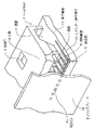
図1は、本発明の第1の実施形態の液体吐出ヘッドの製造方法が適用される液体吐出ヘッドについて説明するための斜視図である。図2は、図1に示される液体吐出ヘッドの、流路方向に沿った断面図である。本発明の液体吐出ヘッドの製造方法は、液体吐出ヘッドを構成するオリフィスプレートの構成材料としてシリコンを用いた際に、シリコンのエッチング技術、薄膜化技術、組み立て技術の要素開発の結果可能となったものである。
【0039】
本実施形態の液体吐出ヘッドの製造方法により製造される液体吐出ヘッドは、図1に示すように、素子基板11の表面に天板15を接合してなるヘッド本体7や、ヘッド本体7の前端面に接合されたオリフィスプレート16などから構成されている。素子基板(以下、ヒーターボードともいう)11には、インクなどの液体を吐出させるために利用される熱エネルギーを発生する複数のエネルギー発生素子(以下、ヒーターともいう)12と、エネルギー発生素子12に電気信号を供給するためのAl配線とが備えられている。この素子基板11は、Si基板上に複数のエネルギー発生素子12および前記Al配線を成膜技術によって形成してなるものである。
【0040】
素子基板11の一面には、エネルギー発生素子12がそれぞれ配置された複数の流路1を形成するための溝や、それぞれの流路1に供給されるインクを一時的に保持する液室2を形成するための溝が形成されている。隣り合う2つの流路1は、それら2つの流路1の間に挟まれる流路側壁8によって仕切られている。液室2および複数の流路2を形成するための溝は、図3に基づいて後述するように、流路側壁8を含む壁部材が素子基板11の一面に貼り付けられることにより形成されている。
【0041】
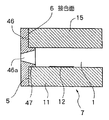
天板15には、液室2内にインクを供給するための供給口4が形成されている。それぞれの流路1にエネルギー発生素子12が配置されるように素子基板11と天板15とが壁部材を介して接合されることにより、複数の流路1および複数のエネルギー発生素子12が備えられたヘッド本体7が構成されている。このヘッド本体7の前端面に、すなわち、図2に示すように素子基板11の、オリフィスプレート16との接合面5、および天板15の、オリフィスプレート16との接合面6を含む面に、それぞれの流路1の開口が配置されている。ヘッド本体7の前端面、すなわち素子基板11の接合面5および天板15の接合面6に接合されたオリフィスプレート16には、流路1とそれぞれ連通した吐出口(以下、オリフィスともいう)3が複数形成されている。
【0042】
この液体吐出ヘッドでは、エネルギー発生素子12から発生した熱エネルギーが流路1内のインクに作用することでエネルギー発生素子12上で気泡が発生し、その気泡の発生を利用して吐出口3からインクが吐出される。
【0043】
図3は、図1および図2に示した液体吐出ヘッドの組み立てについて説明するための斜視図である。図3に示すように、前記素子基板11にヒーター12、ヒーター12を駆動するための回路、およびワイヤーボンデイングやTABボンデイング、ACF接合等により駆動信号や電気エネルギーを外部回路より取り入れるために実装用パッド13が形成されている。これらは汎用的な半導体製造方法により形成することができる。
【0044】
次いで、上記基板に流路側壁8を含む壁部材14が形成される。これら壁部材の形成方法としては、半導体のフォトリソグラフィー技術を適用することができる。通常、これら壁部材は幅5〜15μm程度、高さ10〜100μm程度の為、適用されるフォトリソグラフィー技術としては、メッキや磁気ヘッドに適用される厚膜対応の物が好ましい。また壁形成材料としては、解像性が高く耐インク性を併せ持つことが必要である。最も好適に適用できる材料としては、米国マイクロケミカルコーポレーション社より提供されるSU−8と呼ばれる感光性エポキシレジストを挙げることができる。これらエポキシ樹脂はアルカリ強度の高いインクジェット用のインクでも加水分解することなく、また、エポキシ樹脂の分子量は一般的に低い為、極めてシャープな形状を形成することができる。
【0045】
これら感光性エポキシ樹脂に関しては米国特許4.882.245、4.940.651、5.026.624、5.102.772、5.229.251、5.278.010、5.304.457等に記載される物が何れも適用できる。これら液状樹脂材料はスピンコート法、ロールコート法、スプレー法等にてシリコン基板に塗布、乾燥し、次いで、汎用的なUV露光装置でパターン露光され、露光後のPEB(Post Exposure Bake)を行った後、現像液にて現像することによりパターン形成できる。
【0046】
インク供給孔4を有する天板15は、各種微細加工方法にて作製することが可能である。最も汎用的には、シリコンの異方性エッチング技術を挙げることができる。これは、両面シリコン酸化膜膜を形成したシリコンウエハーに対して汎用的なフォトリソグラフィー技術により酸化膜をパターニングし、アルカリ水溶液にてシリコンをエッチングして貫通孔を形成する技術である。アルカリ水溶液としては、水酸化ナトリウム、水酸化カリウム等の無機アルカリ、TMAH(テトラメチルアンモニウムハイドロキシオキサイド)等の有機アルカリが好適に用いられる。また、ブラスト加工等の砥粒による加工やYAGレーザー等のレーザー加工を適用しても構わない。
【0047】
形成した天板部材は、部材の耐インク性が不十分な場合は表面保護を行うことが必要となる。これは、耐アルカリ性の樹脂を溶剤塗布方法にて塗布する手段を用いても、あるいは、無機材料を蒸着、スパッタリング、CVD等にて成膜する手段の何れも用いても構わない。
【0048】
本発明による液体吐出ヘッドは、シリコン製のオリフィスプレートを適用することにより長尺の液体吐出ヘッドに対しても、線膨張係数の同一部材を用いて対応することを主眼としている為、最も好適には、前述したシリコンの異方性エッチング技術を適用したシリコン製天板が最も好適である。また表面保護としては、被覆性が高く、耐インク性に優れる手段として、窒化シリコンをLP−CVD(Low Pressure Chemical Vapor Deposition)法で形成するか、熱酸化によって酸化シリコンを形成するかが最も好ましい。
【0049】
壁部材を形成したヒーターボードと天板は接着剤等によって貼りあわせる。接着剤は汎用的な接着剤の何れも適用できるが、耐インク性が高いという観点から、エポキシ系接着剤が最も好適である。エポキシとしては、主材と硬化剤が別々の2液タイプ、予め混合されている1液タイプの何れを適用しても構わない。
【0050】
2液タイプの場合、主剤と硬化剤の混合後、上記工程で形成した天板表面、あるいはヒーターボードに形成した壁上面に、スクリーン印刷等の印刷法、転写法、ロールコート法等にて塗布し、天板とヒーターボードを接合して接着剤を硬化せしめれば良い。また、1液タイプの場合は、上記手段にて塗布し、接合後に所定の硬化条件で硬化させれば良い。また、壁材料に用いた感光性エポキシも上記塗布方法により塗布して、UV光の照射にて硬化せしめて接合することも可能である。
【0051】
これら接合した基板は、汎用的なダイサーにて個別のチップに分割してオリフィスプレートを接合する部品が作製される。尚、ダイシング時に切断屑等がインク流路に入ってしまうことを防止する場合は、切断前に汎用的な樹脂を予め溶剤に溶解して、詰め込んで於いても構わない。これら樹脂は、汎用的な溶剤に溶解し、比較的分子量が低く、固い材料が好適に使用できる。最も好適には、クレゾールノボラック、フェノールノボラック等のフェノール樹脂、ポリスチレンやポリ−α-メチルスチレン等のスチレン樹脂を挙げることができる。
【0052】
上記工程で作製したチップとシリコン製オリフィスプレートの貼り付けに関しては、チップ側に予め接着剤を塗布し、次いでオリフィスプレートを位置合わせしつつ接合し、その後接着剤を硬化することにより貼りあわせることができる。接着材料及び塗布方法としては上記した天板とヒーターボードの接着と同一の手段を用いることができる。しかしながら、該接着箇所の場合、接着剤がインク流路内に流れ込んだ場合、吐出不良を招く為、その材料選択と塗布手段がより厳しくなる。2液タイプの接着剤を適用した場合、主剤と硬化剤の混合時点より接着剤の硬化が進行して粘度が経時的に変化する為、厳密な流動性の制御は極めて難しい。また1液タイプを溶剤溶解して塗布した場合、溶剤乾燥時の熱の付与で接着剤がインク流路内に入り込んだり、塗布ムラになったりしてしまう場合が多い。
【0053】
最も好適には、常温にて固体状の接着剤を予めポリエチレンテレフタレート(PET)等のフィルムに塗布、乾燥しておき、これを熱転写法にて上記接合面に転写する手段を挙げることができる。尚、均一な転写が可能となり、またインク吐出口部に接着剤の膜がはらず、良好な接着剤塗布を行うには、材料、接着剤膜厚、転写条件(温度、圧力、プラテンのゴム硬度)等の条件出しが必要となる。
【0054】
上記オリフィスプレートの貼りあわせ工程に於いて、オリフィスプレートに形成したインク吐出口とインク流路の位置ずれを防止する為、前記したようにオリフィスプレートに予め位置決め用の凸部を形成しておけば、簡便な装置で良好な位置合わせが可能となる。また該凸部は、接着剤硬化時に接着剤の粘度が低下しても、インク吐出口に接着剤が流入することを防止できる。
【0055】
オリフィスプレートを接合した後に、シリコン製オリフィスプレートのインク吐出面側に耐インク性の向上とインク濡れ防止の為の撥水剤の塗布を行うことが好ましい。これら塗布材料、塗布方法に関しては、前記した材料、方法が適用できる。
【0056】
このような構成の液体吐出ヘッドを、液体吐出記録装置であるバブルジェットプリンターで用いる場合を考慮すると、近年の写真調の画像を形成するためのインクジェット(インク吐出)としては、2ピコリットルから50ピコリットルくらいの量のインク液滴を周波数10Khzくらいのスピードで吐出させる必要がある。このような量および吐出スピードでインク液滴を吐出させて記録をするには、オリフィスプレート16の厚さは20から100μmくらいで、吐出口3の径が15から30μm程度で形成されれば良い。
【0057】
本発明は、この、オリフィスプレートとして用いられるシリコン基板への穴あけ技術、シリコンの薄膜化技術を研究した結果、達成されたものである。次では、本発明の第1の実施形態に係る液体吐出ヘッドの製造方法として、図1および図2に示したオリフィスプレート16を作製する方法について図4を参照して説明する。
【0058】
図4は、図1および図2に示したオリフィスプレート16を作製する方法について説明するための図である。図4(a)〜図4(e)が断面図であり、図4(a’)、図4(c’)および図4(d’)が斜視図である。ここでは、オリフィスプレート16を作製するためのそれぞれの説明およびそれぞれの図は、1つの液体吐出ヘッド分、すなわち1チップ分のものであるが、実際には、4インチから12インチ程度のシリコンウエハーに数十から数百のチップが配置され、1つのシリコンウエハーから複数のオリフィスプレート16が同時に加工生産される。また、図16は、図4に示される工程において、オリフィスプレートに形成される穴の形状に注目して製造工程のフローを示した断面図である。
【0059】
まず、図4(a)および図4(a’)に示される、厚さ625μm(625ミクロン)のシリコン基板21を準備する。
【0060】
次に、シリコン基板21の表面にAl層を8μmの厚みでスパッタ法により形成する。
【0061】
次に、シリコン基板21上のAl層の表面に、レジストを8μmの厚さで塗付し、図1に示した吐出口3と、シリコン基板21を各チップに分割するための溝状のプレート分割パターンをシリコン基板21に形成するために、塗布された前記レジストのパターニングを行う。Al層の表面に塗布したレジストとしてはシプレイ社製のSJR−5740を用い、そのレジストを塗布する塗付装置としてはキヤノン株式会社製のCDS−600を用い、レジストのパターニングを行うための露光装置としてはキヤノン株式会社製のMPA−600を用いた。
【0062】
次に、パターニングされたレジストをマスクとしてシリコン基板21上のAl層をドライエッチングして、図4(a)および図4(a’)に示されるように、吐出口3に対応する位置に開口部22aを有するパターンが形成されたエッチングマスク用のAl層22をシリコン基板21上に形成する。また、このドライエッチングでは、Al層22に、上述したようなシリコン基板21を分割するための溝状のプレート分割パターンに対応する溝が形成される。ドライエッチング装置としてはアルバック株式会社製のNLD−800の用い、ドライエッチング用のガスとしては塩素を用いた。そのドライエッチング装置では、パワーを1000W、バイアスを100W、圧力を0.8PaとしてAl層のエッチングを行った。
【0063】
次に、Al層22上のレジストをアッシング除去した。
【0064】
次に、図4(b)に示すようにAl層22をマスクにしてシリコン基板21のAl層22側の面における露出した部分をドライエッチングのイオン23によって深堀エッチングして、吐出口3に対応する位置に、50ミクロンに5〜50ミクロンを加えた深さで、図4(c)および図4(c’)に示されるような凹部としての穴21aを複数形成するとともに、シリコン基板21を複数のオリフィスプレートに分割するための溝状のプレート分割パターン21bをシリコン基板21の表面に形成する。プレート分割パターン21bの深さは穴21aの深さと同じように50ミクロンに5〜50ミクロンを加えた値となっている。これにより、それらプレート分割パターン21bおよび複数の穴21aを有するパターンがシリコン基板21の表層に形成される。この工程では、ドライエッチング装置としてアルバック株式会社製のNLD−800を用い、ドライエッチング用のガスとしてはSF6を用いた。そのドライエッチング装置では、パワーを1000W、バイアスを250W、圧力を1.0Paとしてシリコン基板21のエッチングを行い、50μmに5〜50μmを加えた深さの略ストレートな断面形状となる深堀りを実施する。ここで、図16(a)に示すように、SF6のエッチングの後では穴21aの開口面側の端部が、流路側から吐出口側へと徐々に断面積が小さくなる、所謂、テーパー形状を有するテーパー部29aになっており、穴21aの底部を含む穴21aのほとんどの部分が、穴21aの深さ方向の断面形状がほぼ一定のストレート部27bとなっている。このテーパー部29aは表面があれたような状態となるため、このテーパー部29aの表面を滑らかにするために、さらに、エッチング用のガスとしてCF4を用いて、パワーを1000W、バイアスを50W、圧力を1.0Paとしてエッチングを行う。図16(b)に示すようにCF4のエッチングの後では、穴21aの開口面側の端部のテーパー部29cの表面が滑らかになっている。
【0065】
このようにして形成された穴21aに対して、後述するようにシリコン基板21を裏面側からストレート部27dの部分にいたるまで薄くすることで、開口した穴21aの径はシリコン基板21の除去厚のばらつきによらず、ほぼ一定のものが得られる。このとき、穴21aの底部は矩形になっていないことが多いため、除去工程は穴21aが露出した状態で止めるのではなく、確実にストレート部27bにいたるまで行うことが好ましい。本実施形態では、このようにシリコン基板21に吐出口を形成することにより、開口径が均一で、吐出側に断面積が小さくなるテーパー形状の吐出口を得ることができる。
【0066】
図16(a)はSF6のエッチングの後の断面、図16(b)はCF4のエッチングの後の断面を示す。図16(a)に示すようにSF6のエッチングの後では穴21aの開口面側の端部が、テーパー形状を有するテーパー部29aになっており、穴21aの底部を含む穴21aのほとんど部分が、穴21aの深さ方向の断面形状がほぼ一定のストレート部27bとなっている。また、図16(b)に示すようにCF4のエッチングの後では、穴21aの開口面側の端部が、図16(a)に示したテーパー部29aよりも範囲の広いテーパー部29cになっており、穴21aのその他の部分が、深さ方向に断面積が一定のストレート部27dとなっている。従って、ストレート部27dの領域は、図16(a)に示したストレート領域27bの領域よりも狭くなっている。
【0067】
ここでは、バイアスの値を変えることにより、図1および図2に示したような吐出口3のテーパー形状を所望のかたちに形成することができる。
【0068】
次に、図4(c)および図4(c’)に示すようにシリコン基板21上のAl層22を硝酸、リン酸、酢酸の混酸で除去する。次に、シリコン基板21の、インクと接する面を保護するために、シリコン基板21の穴21a側の表面、および穴21aの内壁全体に、図16(c)に示すように、CVDにより保護層としてSiN保護膜26を2ミクロンの厚さで形成する。
【0069】
次に、図4(d)および図4(d’)に示すように、UV剥離テープ24にシリコン基板21の穴21a側の面を貼り付けた後に、シリコン基板21の裏面を研削、研磨して、シリコン基板21を50ミクロンの厚みになるまで薄くした。ここでは、シリコン基板21を研削、研磨する際のシリコン基板21の強度をある程度保持するためのバックグラインンドテープであるUV剥離テープ24にシリコン基板21を貼り付けた。このようにシリコン基板21の裏面を研磨した後、前記UV剥離テープをUV剥離することにより、図4(e)、図4(e’)および図16に示すように、それぞれの穴21aの底部がシリコン基板21の裏面に開口してシリコン基板21を貫通し、シリコン基板21に吐出口3が形成されるとともに、シリコン基板21がプレート分割パターン21bで複数のオリフィスプレート16に分割される。シリコン基板21を薄くする際にはシリコン基板21の裏面をエッチングしてもよい。
【0070】
以上で説明した工程を経て、図4(e)および図4(e’)に示される、シリコン基板21に吐出口3が形成されてなるオリフィスプレート16が作製される。
【0071】
このとき、図16(d)に示すように、吐出口3における断面積が小さい側の開口面は、ストレート部27dにおけるテーパー部29c近傍の部分に形成され、吐出口3の開口面側の先端部に、断面積が一定のストレート部分が残っているため、各吐出口3における吐出口3の開口径を均一にそろえることができる。また、吐出口3全体をテーパー形状とする場合には、吐出口3における断面積が小さい側の開口面が、テーパー部29cとストレート部27dの境界面や、テーパー部29cにおけるストレート部27dの近傍に形成されていてもよい。
【0072】
このようにして得られたオリフィスプレート16を用いて、図3に基づいて上述したのと同様の組み立てを行い、液体吐出ヘッドを作製した。オリフィスプレート16に対する素子基板11および天板15の接着には、2ミクロンの厚みのエポキシ接着剤を用いた。
【0073】
オリフィスプレート16を用いて製造された液体吐出ヘッドを、ポリサルフォン製のオリフィスプレートで作製した比較品とともに、−30度と+60度間のヒートサイクルテストを行った。ポリサルフォン製のオリフィスプレートで作製した比較品が、オリフィスプレートにおけるノズル列方向の長さが50ミリ以上でオリフィスプレートの剥離が生じるのに対し、本発明の製造方法により製造されたシリコン製のオリフィスプレート16で組み立てたものは、そのオリフィスプレート16の剥離が生じなかった。
【0074】
以上で説明したように、本実施形態の液体吐出ヘッドの製造方法では、オリフィスプレート16を作製する際に、シリコン基板21の表面にエッチングにより凹部として穴21aを形成して、シリコン基板21を裏面側から薄くすることにより、そのシリコン基板21に複数の吐出口3が形成されてなるオリフィスプレート16を作製する。これにより、信頼性の高い、長尺化された液体吐出ヘッドを製造することができ、また、そのようにシリコンからなるオリフィスプレートを用いて液体吐出ヘッドを構成する際にも、信頼性の高い、長尺化された液体吐出ヘッドを実現することができる。
【0075】
次に、図4に基づいて説明したオリフィスプレートの製造方法の変形例について図16を参照して説明する。図16は、図4に基づいて説明したオリフィスプレートの製造方法の変形例について説明するための断面図である。図17に基づいて説明するオリフィスプレートの製造方法では、上述した製造方法と比較して、シリコン基板21に吐出口用の穴をドライエッチングにより形成する際に、マスクとして厚さ8μmのAl層の代わりに、厚さ2μmのSiO2層を用いている点が主に異なっている。
【0076】
図17(a)に示すように、シリコン基板21表面に形成された、吐出口およびプレート分割パターンに対応する所定のパターンを有する厚さ2μmのSiO2層28をマスクとしてシリコン基板21のドライエッチングを行い、シリコン基板21に吐出口用の穴21aを形成する。このドライエッチングの工程では、エッチングガスとしてSF6を用いた10秒間のドライエッチングと、エッチングガスとしてCF2を用いた30秒間のドライエッチングと行い、そのようなエッチングを繰り返すサイクルエッチングによりシリコン基板21に複数の穴21aを形成した。
【0077】
このようなSiO2層28をマスクにしたシリコン基板21のドライエッチングでは、深さ方向に断面積が一定な穴21aをシリコン基板21に形成することができる。
【0078】
次に、図17(b)に示すようにSiO2層28の表面全体、および穴21aの内壁面全体にSiN保護膜29をCVD法によって形成する。
【0079】
次に、図17(c)に示すように、シリコン基板21の裏面側からシリコン基板21を薄くすることにより穴21aを貫通させ、シリコン基板21に吐出口3を形成する。吐出口3の開口面は、穴21aの、断面積が一定の領域に形成されている。これにより、シリコン基板21の吐出口3が形成されて構成されるオリフィスプレート16が作製される。
【0080】
図17に基づいて説明したオリフィスプレートの製造方法では、深さ方向に断面積が一定の穴21aの加工を行うことができ、また、穴21aの、断面積が一定の領域に吐出口3の開口が得られる。図17の製造方法により作製されたオリフィスプレートを用いて液体吐出ヘッドを構成することにより、図4および図16の製造方法により作製されたオリフィスプレートを用いて構成された液体吐出ヘッドと同様、信頼性に優れた、長尺化の液体吐出ヘッドを実現することができる。
【0081】
(第2の実施の形態)
図5は、本発明の第2の実施形態の液体吐出ヘッドの製造方法が適用される液体吐出ヘッドについて説明するための斜視図である。図6は、図5に示される液体吐出ヘッドの、流路方向に沿った断面図である。図5および図6に示される液体吐出ヘッドでは、第1の実施形態のものと比較してオリフィスプレートのみが異なっており、オリフィスプレートのヘッド本体側の面における吐出口の周囲に、ヘッド本体の流路に嵌合する凸部が形成されている。図5および図6では、第1の実施形態と同一の構成部品に同一の符号を付してある。以下では、第1の実施形態と異なる点を中心に説明する。
【0082】
本実施形態の液体吐出ヘッドの製造方法により製造される液体吐出ヘッドでは、第1の実施形態で用いたオリフィスプレート16の代わりに、図5および図6に示すようにオリフィスプレート46が用いられている。オリフィスプレート46の構成材料としては第1の実施形態のオリフィスプレート16と同様にシリコンが用いられている。オリフィスプレート16と同様に、オリフィスプレート46は、ヘッド本体7の前端面、すなわち素子基板11の接合面5および天板15の接合面6に接合されており、オリフィスプレート46には、流路1とそれぞれ連通した吐出口46aが複数形成されている。オリフィスプレート46の、ヘッド本体7との接合面における吐出口46aの周囲には、図5および図6に示すように吐出口46aごとにそれぞれ独立した凸部47が複数形成されている。それぞれの凸部47が流路1内に進入し、凸部47が流路1に嵌合した状態で、接合面5,6にオリフィスプレート46が接合されている。
【0083】
図7は、図5および図6に示した液体吐出ヘッドの組み立てについて説明するための斜視図である。図7に示すように、素子基板1の表面に、流路側壁8を含む壁部材14が形成され、壁部材14の素子基板11側と反対側の面に、供給口4が形成された天板15が接合される。そして、素子基板11、壁部材14および天板15の前端面にオリフィスプレート46を貼り付ける。ここで、オリフィスプレート46の凸部47はヘッド本体7の流路1に嵌合させるため、接着剤のエポキシを天板15側および素子基板11側に転写しても、アライメントが正確で、量産性および信頼性に優れた液体吐出ヘッドを製造することができる。
【0084】
次に、本発明の第2の実施形態に係る液体吐出ヘッドの製造方法として、図5および図6に示したオリフィスプレート46を作製する方法について図8を参照して説明する。オリフィスプレート46を作製する工程では、第1の実施形態とほぼ同様の工程を用いるが、プロセスの最初に、シリコン基板上に突起部を形成することにより、吐出口46aに対応する位置およびその周辺に高さ約4ミクロンの凸部を形成する点が異なる。
【0085】
図8は、図5および図6に示したオリフィスプレート46を作製する方法について説明するための図である。図8(a)〜図8(e)が断面図であり、図8(a’)、図8(c’)および図8(d’)が斜視図である。ここでは、オリフィスプレート46を作製するためのそれぞれの説明およびそれぞれの図は、1つの液体吐出ヘッド分、すなわち1チップ分のものであるが、実際には、4インチから12インチ程度のシリコンウエハーに数十から数百のチップが配置され、1つのシリコンウエハーから複数のオリフィスプレート46が同時に加工生産される。
【0086】
まず、厚さ625μm(625ミクロン)のシリコン基板を準備する。そのシリコン基板の表面にレジストを2ミクロンの厚さで塗布し、吐出口46aに対応する位置およびその周囲に、高さ約4ミクロンの凸部47を形成するために、そのレジストのパターニングを行う。ここで、レジストとしてはシプレイ社製のSJR−5740を用い、そのレジストを塗布する塗付装置としてはキヤノン株式会社製のCDS−600を用い、レジストのパターニングを行うための露光装置としてはキヤノン株式会社製のMPA−600を用いた。
【0087】
次に、パターニングされたレジストをマスクとして前記シリコン基板をドライエッチングすることにより、図8(a)および図8(a’)に示される、表面に突起部31bが複数形成されたシリコン基板31を作製する。突起部31bの高さは約4ミクロンであり、それぞれの突起部31bは、図5および図6に示した吐出口46aに対応する位置およびその周囲に形成されている。ここで、ドライエッチング装置としてはアルバック株式会社製のNLD−800の用い、ドライエッチング用のガスとしてはSF6を用いた。そのドライエッチング装置では、パワーを1000W、バイアスを50W、圧力を0.8Paとし、3分間の時間でシリコン基板31のエッチングを行った。
【0088】
次に、シリコン基板31の突起部31b側の表面に、その突起部31bを覆うようにAl層を8ミクロンの厚みでスパッタ法により形成する。
【0089】
次に、シリコン基板31上のAl層の表面に、レジストを8ミクロンの厚さで塗付し、図5に示した吐出口46aと、シリコン基板31を各チップに分割するための溝状のプレート分割パターンをシリコン基板31に形成するために、塗布された前記レジストのパターニングを行う。Al層の表面に塗布したレジストとしてはシプレイ社製のSJR−5740を用い、そのレジストを塗布する塗付装置としてはキヤノン株式会社製のCDS−600を用い、レジストのパターニングを行うための露光装置としてはキヤノン株式会社製のMPA−600を用いた。
【0090】
次に、パターニングされたレジストをマスクとしてシリコン基板31上のAl層をドライエッチングして、図8(a)および図8(a’)に示されるように、吐出口46aに対応する位置に開口部32aを有するパターンが形成されたエッチングマスク用のAl層32をシリコン基板31上に形成する。また、このドライエッチングでは、Al層32に、上述したようなシリコン基板31を分割するための溝状のプレート分割パターンに対応する溝が形成される。ドライエッチング装置としてはアルバック株式会社製のNLD−800の用い、ドライエッチング用のガスとしては塩素を用いた。そのドライエッチング装置では、パワーを1000W、バイアスを50W、圧力を0.8PaとしてAl層のエッチングを行った。
【0091】
次に、Al層32上のレジストをアッシング除去した。
【0092】
次に、図8(b)に示すようにAl層32をマスクにしてシリコン基板31のAl層32側の面における露出した部分をドライエッチングのイオン33によって深堀エッチングして、吐出口46aに対応する位置に、70ミクロンに5〜50ミクロンを加えた深さで、図8(c)および図8(c’)に示されるような凹部としての穴31aを複数形成するとともに、シリコン基板31を複数のオリフィスプレートに分割するための溝状のプレート分割パターン31cをシリコン基板31の表面に形成する。プレート分割パターン31cの深さは穴31aの深さと同じように70ミクロンに5〜50ミクロンを加えた値となっている。これにより、それらプレート分割パターン31cおよび複数の穴31aを有するパターンがシリコン基板31の表層に形成され、また、突起部31bの残った部分によって、図5および図6に示した凸部47が構成され、シリコン基板31上に複数の凸部47が形成されることになる。この工程で、ドライエッチング装置としてアルバック株式会社製のNLD−800の用い、ドライエッチング用のガスとしてはSF6を用いた。そのドライエッチング装置では、パワーを1000W、バイアスを200W、圧力を1.0Paとしてシリコン基板31のエッチングを行った。
【0093】
次に、図8(c)および図8(c’)に示すようにシリコン基板31上のAl層22を硝酸、リン酸、酢酸の混酸で除去する。次に、シリコン基板31の、インクと接する面を保護するために、シリコン基板31の穴31a側の表面全体、および穴31aの内壁全体にCVDにより保護層としてSiN層(不図示)を2ミクロンの厚さで形成する。
【0094】
次に、図8(d)および図8(d’)に示すように、UV剥離テープ34にシリコン基板31の穴31a側の面を貼り付けた後に、シリコン基板31の裏面を研削、研磨して、シリコン基板31の、凸部47の高さを含んだ厚みが70ミクロンになるまでシリコン基板31薄くした。ここでは、シリコン基板31を研削、研磨する際にシリコン基板31を強度をある程度保持するために、UV剥離テープ24にシリコン基板31を貼り付けた。このようにシリコン基板31の裏面側の層を除去することにより、図8(e)および図8(e’)に示すように、それぞれの穴31aの底部がシリコン基板31の裏面に開口して穴31aがシリコン基板31を貫通し、シリコン基板31に吐出口46aが形成されるとともに、シリコン基板31がプレート分割パターン31cで複数のオリフィスプレート46に分割される。これにより、シリコン基板31に複数の凸部47および複数の吐出口46aが形成されてなるオリフィスプレート46が製造される。
【0095】
作製したオリフィスプレートは接着剤等により、エネルギー発生素子及び流路が配置されたヘッド本体に貼り付けることにより、液体吐出ヘッドが形成される。接着剤は耐インク性、接着強度が高いエポキシ樹脂が最も好ましい。エポキシ樹脂としては、汎用的な2液タイプの物、1液タイプの高温硬化タイプの物、何れも使用できる。しかしながら、これら接着剤を硬化する場合、オリフィスプレートは吐出エレメントに荷重を付与しつつ硬化させる必要がある為、荷重付与時にずれてしまう場合がある。また、接着剤がはみ出してインク吐出口を埋めてしまう場合もある。該弊害を防止する為、オリフィスプレートの接合側、吐出口の周囲に凸部を形成することが好ましい。この凸部をインク流路に嵌め込むことにより、接合時のインク流路と吐出口の位置ずれを防止することができる。また該凸部は接着剤のはみ出しに際して、該凸部で接着剤がメニスカスを形成して流入が停止する為、インク吐出口に接着剤が入り込むことを防止できる。
【0096】
(第3の実施の形態)
図9は、本発明の第3の実施形態の液体吐出ヘッドの製造方法について説明するための図である。図10は、図9に基づいて説明するオリフィスプレートの製造工程のフローチャートである。
【0097】
本実施形態の液体吐出ヘッドの製造方法は、第2の実施形態の製造方法のさらに発展した形態である。インクジェット記録の一般的な応用として、黒、シアン、マゼンタ、イエローの4色の記録、もしくは、さらに淡シアン、淡マゼンタを加えた6色の記録が用いられる。ここで、各色のインク同士の互いの着弾位置の位置合わせをするには、それぞれの色のノズルの相対的な位置を合わせる必要があり、1枚のオリフィスプレートでそれぞれの色のノズルを位置合わせすることが望ましい。本実施形態の液体吐出ヘッドの製造方法では、第1および第2の実施形態におけるシリコン基板の薄膜化の時にシリコン基板をUV剥離テープで補強する代わりに、シリコン、またはシリコンと線膨張係数の近いガラスからなる枠体でシリコン基板を補強することにより、コストダウンを測りながらノズル列の位置合わせが達成される。
【0098】
まず、図9(a)に示されような穴54が形成された板状の枠体53、および図9(b)に示されるような突起部52が形成されたシリコン基板51を作製する。枠体53の構成材料としては、シリコン、またはシリコンと線膨張係数の近いガラスを用いることができる。本実施形態では、枠体53の構成材料として、シリコンと線膨張係数の近いガラスを用いた場合を例にとって説明する。
【0099】
枠体53を作製する際には、まず、厚さ625μm(625ミクロン)のガラスウエハーを準備し、そのガラスウエハーに対して穴54のパターニングを行う。ここで、枠体53の材料としては、シリコンと線膨張係数の近いHOYA社製のSG−2を用い、穴54を形成するための加工はブラストにより行った。
【0100】
また、複数の突起部52が形成されたシリコン基板51を作製する際には、第2の実施形態と同様に、まず、厚さ625μm(625ミクロン)のシリコン基板を準備し、そのシリコン基板の表面全体にレジストを2μmの厚さで塗布する。次に、そのシリコン基板の表面における吐出口に対応する位置およびその周囲に高さ約4μmの突起部52を形成するための、シリコン基板上のレジストのパターニングを行う。ここでは、第2の実施形態と同様に、レジストとしてはシプレイ社製のSJR−5740を用い、そのレジストを塗布する塗付装置としてはキヤノン株式会社製のCDS−600を用い、レジストのパターニングを行うための露光装置としてはキヤノン株式会社製のMPA−600を用いた。
【0101】
次に、パターニングされたレジストをマスクとして前記シリコン基板をドライエッチングすることにより、図9(b)に示されるような、下地として表面に突起部52が複数形成されたシリコン基板51を作製する。突起部52の高さは約4ミクロンであり、それぞれの突起部52は、吐出口に対応する位置およびその周囲に形成されている。また、図9(b)に示される状態のシリコン基板51では、突起部52の高さを含む厚みaが、シリコン基板51のもとの厚さと同じ625μmとなっている。ここで、第2の実施形態と同様に、ドライエッチング装置としてはアルバック株式会社製のNLD−800の用い、ドライエッチング用のガスとしてはSF6を用いた。そのドライエッチング装置では、パワーを1000W、バイアスを50W、圧力を0.8Paとし、3分間の時間でシリコン基板31のエッチングを行った。
【0102】
次に、突起部52を形成するために用いた、シリコン基板51上のレジストをアッシング除去した後に、シリコン基板51の突起部52側の面上に不図示の熱酸化膜(SiO2)を1μmの厚さで形成する。これにより、突起部52の先端面および側面全体にも熱酸化膜が形成される。次に、シリコン基板51上のその熱酸化膜の表面全体にレジストを塗布し、塗布されたレジストの、吐出口に対向する位置に開口部が形成されるようにそのレジストのパターニングを行う。そして、パターニングされたレジストをマスクとして、シリコン基板51上の熱酸化膜をドライエッチングによりパターニングする。このパターニングにより、シリコン基板51上の熱酸化膜には、吐出口に対応する位置に開口部が形成される。この熱酸化膜は、後述するように吐出口を形成するためにドライエッチングによりシリコン基板51に凹部を形成する際にマスクとして用いられる。
【0103】
次に、シリコン基板51上の熱酸化膜をパターニングするために用いられたレジストをアッシング除去する。
【0104】
次に、図9(c)に示すように、シリコン基板51の突起部52が枠体53の穴54の内部に配置されるように、シリコン基板51の突起部52側の面に枠体53を陽極接合する。ここでは、シリコン基板51と枠体53との貼り合わせ装置としてカールズース株式会社製のSB−6を用いた。その貼り合わせ装置では、温度を350度とし、1時間でシリコン基板51と枠体53との陽極接合を行った。本実施形態では、シリコン基板51と枠体53とを陽極接合したが、陽極接合の代わりに真空加熱接合、または接着剤を用いた接合によりシリコン基板51と枠体53とを接合してもよい。
【0105】
次に、図9(d)に示すように、上述したシリコン基板51上の熱酸化膜(不図示)をマスクにしてシリコン基板51の突起部52の先端面における露出した部分をドライエッチングのイオン56によって深堀エッチングして、吐出口に対応する位置に凹部として、50ミクロンに5〜50ミクロンを加えた深さの穴58を複数形成する。図9(d)に示されるように、突起部52の残った部分が、ヘッド本体7の流路1に嵌合する凸部57となる。
【0106】
次に、図9(e)に示すように、シリコン基板51の裏面を研削、研磨し、シリコン基板51の、凸部57の高さを含んだ厚みbが50ミクロンになるまでシリコン基板51を薄くする。このようにシリコン基板51を薄くすることにより、図9(c)に示されるように、それぞれの穴58の底部がシリコン基板51の裏面に開口して穴58がシリコン基板51を貫通し、シリコン基板51に吐出口58aが形成される。
【0107】
次に、吐出口58aの内壁面全体に保護膜としてのSiN膜をCVD法によって2ミクロンの厚さで形成する。本実施形態では、その保護膜の構成材料として窒化シリコンを用いたが、窒化シリコンの代わりに、熱酸化膜、CVD法による酸化シリコンもしくは、炭化シリコン、金属めっき、スパッタによるの金、白金、Pd、Cr、Ta、Wのうちのいずれかを用いてもよい。
【0108】
次に、図9(f)に示すように、シリコン基板51の凸部57側と反対側の面に、それぞれの吐出口58aが塞がれないように撥水フッ素膜59をラミネート転写する。
【0109】
次に、図9(g)に示すように、液体吐出ヘッド部4個、すなわち素子チップ4個に相当するノズル4列分のオリフィスプレートの切り出しをダイシングにより行う。これにより、シリコン基板51に4列の凸部57および吐出口58aが形成されてなるオリフィスプレート51aが切り出される。
【0110】
次に、上述した工程とは別の工程で作製された、素子基板11に天板15を接合してなるヘッド本体7を、シリコン基板51と枠体53とが接合されてなるものに接合するために、ヘッド本体7における流路1の開口端が位置する前端面にエポキシ樹脂を転写する。そして、シリコン基板51と枠体53とが接合されてなるものの穴54にヘッド本体7の前端面を向けて穴54にヘッド本体7を挿入し、オリフィスプレート51aに対してヘッド本体7の位置決めを行う。オリフィスプレート51aとヘッド本体7との位置決めは、ヘッド本体7の流路1内にオリフィスプレート51aの凸部57を嵌合させることにより行う。
【0111】
このように、オリフィスプレート51aとヘッド本体7とのアライメントをしてオリフィスプレート51aにヘッド本体7を接着する。
【0112】
次に、ヘッド本体7と枠体53との空隙を、金属の微粒子が添加された高い熱伝導性を有する熱伝導樹脂を充填し、その空隙を封止する。これにより、ヘッド本体7と枠体53との熱伝導を確保しながら、4列のノズル列を有する液体吐出ヘッドの強度が高められる。
【0113】
図11は、オリフィスプレートに枠体が接合されてなるものに4つのヘッド本体が接着されて構成された液体吐出ヘッドを示す斜視図である。図11に示すように、枠体53の4つの穴54のそれぞれにヘッド本体7を挿入して、上述した方法によりそれぞれのヘッド本体7をオリフィスプレート51aに接合することで液体吐出ヘッドが作製される。
【0114】
以上で説明した工程を経て、1枚のオリフィスプレートで位置合わせされて一体化された、4列のノズル列を有する液体吐出ヘッドが製造される。
【0115】
(第4の実施の形態)
図12は、本発明の第4の実施形態の液体吐出ヘッドの製造方法として、液体吐出ヘッドのオリフィスプレートを作製する工程について説明するための図である。図12(a)〜図12(g)が断面図であり、図12(a’)、図12(c’)、図12(e’)および図12(g’)が斜視図である。
【0116】
本実施形態の液体吐出ヘッドの製造方法では、第1の実施形態の製造方法と比較して、オリフィスプレートを作製する際に吐出口の内面に形成された保護膜を、そのオリフィスプレートのヘッド本体側と反対側の面から突出させて突出部を形成する点が異なっている。
【0117】
まず、図12(a)および図12(a’)に示される、厚さ625μm(625ミクロン)のシリコン基板71を準備し、シリコン基板71の表面にAl層を8ミクロンの厚みでスパッタ法により形成する。
【0118】
次に、シリコン基板71上のAl層の表面に、レジストを8ミクロンの厚さで塗付し、吐出口と、シリコン基板71を各チップに分割するための溝状のプレート分割パターンをシリコン基板71に形成するために、塗布された前記レジストのパターニングを行う。
【0119】
次に、パターニングされたレジストをマスクとしてシリコン基板71上のAl層をドライエッチングして、図12(a)および図12(a’)に示されるように、吐出口に対応する位置に開口部72aを有するパターンが形成されたエッチングマスク用のAl層72をシリコン基板21上に形成する。また、このドライエッチングでは、Al層72に、上述したようなシリコン基板71を分割するための溝状のプレート分割パターンに対応する溝が形成される。
【0120】
次に、Al層22上のレジストをアッシング除去する。
【0121】
次に、図12(b)に示すようにAl層72をマスクにしてシリコン基板71のAl層72側の面における露出した部分をドライエッチングのイオン73によって深堀エッチングして、吐出口に対応する位置に、70ミクロンに5〜50ミクロンを加えた深さで、図12(c)および図12(c’)に示されるような凹部としての穴71aを複数形成するとともに、シリコン基板71を複数のオリフィスプレートに分割するための溝状のプレート分割パターン72bをシリコン基板21の表面に形成する。プレート分割パターン72bの深さは、穴71aの深さと同じように70ミクロンに5〜50ミクロンを加えた値となっている。これにより、それらプレート分割パターン72bおよび複数の穴71aを有するパターンがシリコン基板71の表層に形成される。
【0122】
次に、図12(c)および図12(c’)に示すようにシリコン基板71上のAl層72を硝酸、リン酸、酢酸の混酸で除去する。
【0123】
次に、図12(d)に示すようにシリコン基板71の、インクと接する面を保護するために、シリコン基板71の穴71a側の表面、および穴71aの内壁全体に、SiN層からなる保護膜75をCVD法により2ミクロンの厚さで形成する。本実施形態では、その保護膜75の構成材料として窒化シリコンを用いたが、窒化シリコンの代わりに、熱酸化膜、CVD法による酸化シリコンもしくは、炭化シリコン、金属めっき、スパッタによるの金、白金、Pd、Cr、Ta,Wのうちのいずれかを用いてもよい。また、保護膜の厚みは0.5〜2μmが好ましい。これは、保護膜が厚すぎると応力が大きくなるためシリコン基板の検索、研磨時に割れやすくなるためであり、また、突出部は親水性を有するためこのの親水部分が多いと液滴がよれやすくなるためである。
【0124】
次に、図12(e)および図12(e’)に示すように、UV剥離テープ74にシリコン基板71の穴71a側の面を向けてUV剥離テープ74上にシリコン基板71を貼り付けた後に、シリコン基板71の裏面を研削、研磨して、シリコン基板71を70ミクロンの厚みになるまで薄くした。ここでは、シリコン基板71を研削、研磨する際にシリコン基板71を強度をある程度保持するために、UV剥離テープ74にシリコン基板71を貼り付けた。このようにシリコン基板71の裏面を研磨することにより、図12(f)に示すように、それぞれの穴71aがシリコン基板71を貫通してシリコン基板71に吐出口71bが形成されるとともに、シリコン基板71がプレート分割パターン72bで複数のオリフィスプレート76に分割される。
【0125】
次に、図12(g)および図12(g’)に示すように、シリコン基板71における保護膜75によって覆われていない側の表面の表層を、KOHによるアルカリエッチングにより除去し、シリコン基板71のその表面から保護膜75を突出させて突出部75aを形成する。これにより、液体吐出ヘッドのヘッド本体に接合されるオリフィスプレート76が作製され、吐出口71bの内壁を構成する保護膜75がオリフィスプレート76の表面から突出した吐出部が形成されることになる。
【0126】
図13は、図12の工程により作製されたオリフィスプレート76を用いた液体吐出ヘッドの組み立てについて説明するための斜視図である。上述した工程によりオリフィスプレート76を作製した後、図13に示すように素子基板11、壁部材14および天板15からなるヘッド本体7にオリフィスプレート76を接合する組み立てを行い、液体吐出ヘッドを作製する。ここで、オリフィスプレート76における吐出部75aが形成された面が、ヘッド本体7側と反対側になるようにオリフィスプレート76を接合する。
【0127】
このオリフィスプレート76を用いた液体吐出ヘッドの場合、SiNからなる保護膜75はインクに対して撥水性を有しているので、ブレードによって吐出口面を拭くことによる、ノズル周りのクリーニングが不要となり、液体吐出記録装置の本体の構造、およびその制御シーケンスが単純化される。
【0128】
図14は、図12に基づいて説明したオリフィスプレートの製造方法の変形例について説明するための図である。図14に基づいて説明するオリフィスプレートの製造方法は、上述した図12(g)および図12(g’)の工程までは図12の製造方法と同じであり、図12(g)および図12(g’)の工程の後にオリフィスプレート76のシリコン基板71の表面に撥水膜を形成する。
【0129】
図12(g)および図12(g’)の工程の後には、図14(a)および図14(a’)に示すように、オリフィスプレート76を構成するシリコン基板71の露出している表面、すなわちシリコン基板71における保護膜75が突出して吐出部75aが形成された表面全体に、ディスペンサー78によって撥水材79をディスペンス塗布する。これにより、図14(b)および図14(b’)に示すようにシリコン基板71の表面における突出部75aの周囲を含んだその表面全体に、撥水膜79aを形成する。
【0130】
撥水膜79aが形成されたオリフィスプレート76を用いて構成された液体吐出ヘッドの場合、オリフィスプレート76の吐出口面における吐出口周辺でインクの付着が防止されるので、そのようなインク付着による吐出インクのよれが発生しにくい構造となる。
【0131】
このようなシリコンオリフィスプレートの製造方法により、撥水膜がノズル周辺にも形成され、ノズル周辺のインク付着による吐出液滴のよれが発生しにくい液体吐出ヘッドを提供することができる。
【0132】
本実施形態の液体吐出ヘッドの製造方法では、オリフィスプレート76のヘッド本体側の面には、そのヘッド本体の流路内に進入して嵌合する凸部を形成していないが、本実施形態に第2の実施形態の製造方法を適用して、ヘッド本体の流路に嵌合する凸部を有するとともに、吐出口の内壁を構成する保護膜を突出させた構造の液体吐出ヘッドを製造してもよい。
【0133】
(第5の実施の形態)
図18は、本発明の第5の実施の形態の液体吐出ヘッドの製造方法について説明するための図である。
【0134】
本実施形態は、凹部形成後あるいは凹部のシリコン側壁保護膜形成を行った後、凹部に詰め物をすることが上述の実施形態と異なっている。上述の実施形態では、該貫通孔に研磨剤が入ったり、研削時にチッピングが起きたりして、吐出が不安定になる場合がある。本実施形態では、凹部に詰め物をすることにより、シリコン基板を薄くする工程において、特別なコントロールをすることなく、それらを容易に防止することができる。
【0135】
以下に、図18に基づいて本実施形態における液体吐出ヘッドの製造方法を説明する。
【0136】
まず、シリコン基板201に位置ずれ防止の凸部201bを形成するための突起部を形成する(101、図18(a))。
【0137】
該凸部201bの形成方法は、凹部201a形成前に予めドライエッチングによりシリコンを加工し、突起部202を形成しておけば良い。尚、該突起部は汎用的なポジ型レジストをマスクにフッ素系ガスでエッチングすれば容易に形成できる。前記凸部202は1〜10μm程度の高さが好適に使用できる。インク流路との嵌合に際しては、オリフィスプレート接合装置の接合精度に左右されるが、一般的には0.5〜3μm程度の隙間ばめ位が好ましい。
【0138】
次に、ドライエッチングにてインク吐出口となる凹部201aを形成する。このときプレートの外形形状に対応するプレート分割パターンも一括して形成する(102、図18(b))。
【0139】
ドライエッチングによる前記凹部201aおよびプレート分割パターンの形成は、マスク部材をパターニングにより形成し、該パターンをマスクとし、フッ素系ガスをエッチャントとして適用できる。マスクパターンは汎用的なレジストであっても構わないし、Al、Ta、W等の金属や酸化シリコン、窒化シリコン等を用いても構わない。エッチング深さは、最終的に形成されるオリフィスプレートの厚さ以上であれば、薄膜化工程によりインク吐出口となる貫通孔が形成される。勿論、必要以上に深くエッチングすることは、凹部形状の劣化やタクトUPを招くし、余りにオリフィスプレートの厚さに近接した場合は、ローデイング効果により未貫通部が生じる弊害を招く。
【0140】
エッチング深さは、吐出口の深さに対して、5〜50μm加えた深さをエッチングすることが最も好ましい。即ち、最終的なオリフィスプレートの厚さを50μmと設計した場合、該凹部深さは55〜100μm程度が好ましい。
【0141】
エッチング手段としては、汎用的なリアクチーブイオンエッチング(RIE)を適用しても構わないし、また高速でエッチングする為、電子サイクロトロン(ECR)型、マグネトロン型、誘導結合型等のエッチング手段を適用しても構わない。
【0142】
最も好ましくは、ICP−RIE、Boschプロセスと呼ばれる、ICPのエッチングとエッチング部側壁の保護膜のデポジットを高速で繰り返す凹部形成手段である。
【0143】
該エッチングに於いては、SF6,CF4,NF3等の高速エッチングを可能とするエッチャントでエッチングした後、アンダーカットを防止する為、CHF3,C2F4,C2F6,C2H2F2,C4F8等のデポジットガスでフッ素系ポリマーを側壁に形成し、該工程を繰り返すことにより、高速でアスペクト比の高い凹部形状およびプレート分割パターン形状を形成することができる。該エッチングプロセスを導入したエッチング装置はアルカテル社、STS社より提供されている。次に、耐インク性向上のためにインク吐出口内部に側壁保護皮膜206を形成する(103、図18(c))。
【0144】
インクジェット用のインクはアルカリ性の場合が多く、シリコンをエッチングする場合がある。このようなインクを適用する場合にシリコン面を保護する必要がある。シリコン面の保護は、RIEで形成したトレンチ穴側壁とインク吐出口面の両者がある。トレンチ穴の側壁に関しては、RIE工程の後、汎用的な成膜手段で耐インク性の保護膜を形成すれば良い。汎用的な保護膜形成方法としては、熱酸化や、CVD、スパッタリング、メッキ等がある。また保護膜材料としては、酸化シリコン、窒化シリコン等のシリコン化合物、金、白金、Pd、Cr、Ta、W、等の金属等何れの材料でも構わない。最も好ましくは、熱酸化により酸化シリコンを形成する、あるいはLP−CVDにより窒化シリコンを形成する手段がコストも安価で、被覆性が高い。これら、保護膜の厚さは0.1から5μm程度が好適である。
【0145】
次に、凹部内部に詰め物を埋め込む(104、図18(d))。
【0146】
バックグラインディングやエッチング、研磨時に貫通孔が形成される為、該貫通孔に研磨剤が入ったり、研削時にチッピングが起きたりして、吐出が不安定になる場合がある。これを防止する手段として、凹部形成後あるいは凹部のシリコン側壁保護膜形成を行った後、凹部201aに詰め物210をする手段を挙げることができる。最も簡便な手段としては樹脂を溶剤に溶解して埋め込み、溶剤を乾燥除去した後にシリコンの薄膜化をする方法を挙げることができる。埋め込む樹脂としては、研削、研磨時に発生する温度以上の軟化温度を有し、チッピングを防止できる硬さを有し、また加工後に容易に溶解除去できる樹脂が好ましい。一般的にはフェノールノボラック、クレゾールノボラック、ポリビニルフェノール等のフェノール樹脂、ポリスチレンやポリ−α−メチルスチレン等のスチレン樹脂、ポリメチルメタクリレート、ポリメチルメタクリル酸等のアクリル樹脂等が好適に使用できる。これら樹脂は溶剤に溶解した後、スピンコート法等によりシリコンウエハー上に塗布し、オーブン等で乾燥することにより凹部201aに簡便に埋め込むことができる。また、この時凹部201aに気泡が残存するようであれば、真空中にて塗布することも構わない。
【0147】
樹脂以外には金属を埋め込むことも可能である。これら金属はスパッタリングや蒸着、CVD等により埋め込み、シリコン薄膜化後に酸等により溶解除去できる。埋め込む金属としては、TaやW、Cr、Ni等固い金属が好適に使用できる。
【0148】
次に、バックグラインディングテープであるUV剥離テープを貼り付ける(105、図18(e))。バックグラインディングテープは、シリコン基板を研削、研磨する際のシリコン基板の強度をある程度保持するため保持部材として用いられる。
【0149】
次に、前記シリコン基板の裏面を研削するにより前記シリコン基板201を薄くし(106、図18(f))、さらに、研磨するにより保護膜のチッピング部を除去して(107、図18(f))シリコン基板201を薄膜化することにより、インク吐出口となる貫通孔の形成されたオリフィスプレート216を形成することができる。
【0150】
シリコン基板201の薄膜化は、表面にUV剥離テープ204を貼りあわせた後、裏面より研削(バックグラインディング)にて高速で加工した後、薄膜シリコンの強度を高める為、研削で生じたマイクロクラックを研磨やエッチングで除去する手段が一般的である。バックグラインディングは通常、#100〜#500番程度の砥石で粗削りを行った後、#1500〜#3000番程度の砥石で仕上げ研削を行う。また、厚さ100μm以下の薄膜オリフィスプレートを形成する場合、前記したように、研削時のマイクロクラックが強度低下を招く為、研磨やエッチングにより該クラックを除去することが一般的である。研磨は汎用的なアルミナやシリカ、酸化セリウム等を使用できる。またエッチングの場合はフッ酸、あるいはフッ酸と硝酸の混合液、水酸化ナトリウムや水酸化カリウム、テトラメチルアンモニウムハイドレート等のアルカリ溶液が使用できる。これらシリコンの薄膜化装置としては岡本工作機械株式会社や東京精密株式会社等から、上記工程をインライン化した量産装置が提供されている。
【0151】
次に、吐出口周囲にエッチングにより保護膜206を突出させて突出部206aを形成する(108、図18(g))。
【0152】
前記シリコン基板201の薄膜化に際して、シリコン凹部の側壁保護材料として所定材料を選択し、薄膜化後にエッチングを行うことにより、インク吐出口周囲に突出部206aを形成できる。該突出部206aはインク吐出に吐出口面に付着したインク液的がインク吐出口に流入して吐出不良を起すことを防止したり、また、インク吐出口面の保護樹脂を塗布する工程での、該樹脂が吐出口内に流入することを防止したりできる。
【0153】
例えば、凹部側壁の保護材料として窒化シリコンを用いた場合、薄膜化後にフッ酸あるいは、フッ酸と硝酸の混合液でエッチングすれば、窒化シリコンのみ残存して突出部となる。またシリコンの熱酸化によって側面保護を行った場合、アルカリ溶液でエッチングすれば酸化シリコンの突出部206aを形成することができる。該突出部206aの高さは保護皮膜の膜厚との相関もあるが、0.5〜10μm程度が好ましい。該突出部206aの高さが高すぎる場合は、液体吐出ヘッド使用時の吐出面のブレード拭き時に欠け等が発生する。
【0154】
次に、UV剥離テープをUV剥離し(109、図18(h))、さらに、前記詰め物210を溶解除去する(210、図18(i))ことにより、前記オリフィスプレート306を作製した。なお、UV照射は古河電工株式会社製UVM−200を用い、照射量は2J/cm2とした。
【0155】
次に、インク吐出口面を保護する皮膜を形成する。
【0156】
インク吐出口面の保護は、シリコンを薄膜化した後に上記した方法で耐インク性の材料を成膜しても構わないし、該オリフィスプレートを貼りあわせて液体吐出ヘッドを作製した後、吐出口面に耐インク性の樹脂を塗布しても構わない。最も好ましくは、フッ素系樹脂、シリコン系樹脂を塗布して撥水膜を形成すれば、インクに対する撥水性を発現でき、インク吐出口面がインクで濡れることがなく、良好な印字を実現できる。
【0157】
これらフッ素系樹脂としては、旭硝子株式会社から提供されるサイトップ、信越化学工業株式会社から提供されているSIFEL他何れのフッ素系化合物を用いても構わない。これら保護樹脂の塗布方法としては、転写法、ディスペンス法等が好適に使用できる。転写法としては、上記樹脂溶液をスピンコートやバーコート等のソルベントコート法にて樹脂やゴム膜上に薄膜塗布し、そのままインク吐出口面に押し当てて転写する方法が一般的である。また、転写し難い場合は熱等を付与しても構わない。
【0158】
最も好適に使用できる樹脂は上記したサイトップであり、該樹脂の溶剤CT−Solv180に1〜5wt%の濃度で希釈し、シリコンゴムを貼り付けたシリコンウエハー上にスピンコートして薄膜化し、そのまま転写する方法が好適に使用できる。
【0159】
最後に、上述した工程とは別の工程で作製した素子基板に天板を接合してなるヘッド本体に、上述した工程で作製されたオリフィスプレート216を接合することにより、液体吐出ヘッドを作製した。
【0160】
なお、前記詰め物210の除去は、前記オリフィスプレートをヘッド本体に接合した後に行ってもよい。
【0161】
このような液体吐出ヘッドの製造方法により、前記基板を薄くする工程において、特別なコントロールをすることなく、研削時にチッピングが起こったり、研磨時に吐出口となる貫通孔に研磨剤が入ったりすることを容易に防ぐことができ、吐出の安定した液体吐出ヘッドを提供することができる。
【0162】
(第6の実施の形態)
図20は、第6の実施の形態の液体吐出ヘッドの製造方法について説明するための図である。
【0163】
本実施形態は、第1の実施形態と比較して、シリコン基板としてシリコンウエハー301を使用することおよび該シリコンウエハー301の外周部を残してプレート分割パターン301bを形成することが異なっている。
【0164】
本実施形態は、シリコンウエハー301の分割方法に関して特開平9-213662号公報の記載、いわゆる「先ダイシング」を利用したものとなっている。「先ダイシング」は、半導体素子が形成されたウエハー上に格子状に配置されたダイシングラインに沿って前記半導体素子の形成面側から所定の厚さまでダイシングすることにより溝を形成し、前記ウエハーにおける半導体素子の形成面上にバックグラインディングテープを貼り付け、前記ウエハーの裏面を前記溝に達するまで研削及び研磨し、ウエハーを個々のチップに分割することを特徴としている。
【0165】
ここで、本実施形態では、ウエハーにプレート分割パターン(溝)を形成する点と、プレート分割パターンを形成した後に、その裏面からウエハーを研削してウエハーを分割する点は、「先ダイシング」と、同一である。また、プレート分割パターンを形成した面にバックグラインディングテープを貼り付ける点が、本実施形態においてウエハーの強度を保持するためにUV剥離テープを貼り付ける点と類似している。
【0166】
しかし、「先ダイシング」を利用した場合、プレート分割パターンをダイシングによって形成するため、ウエハーの外周部までダイシング溝が入る。一方、シリコンウエハーの外周2〜5mmはウエハーの有効範囲外の領域であり、ウエハーの厚さが薄く、またパターンも形成しない領域である。したがって、外周部の分割されたシリコンはバックグラインディングテープに対する保持力が弱く、バックグラインディングや研磨工程で、いわゆるチップ飛びが発生して、良品チップを破壊してしまう可能性がある。また、ウエハーの薄膜化後にはシートによってのみオリフィスプレート(チップ)が保持されるため、ウエハーの剛性が低下することにより、搬送、カセットへの挿入の際に、たわみが生じ、搬送トラブル、衝突による割れが起こり易い。また、ダイシングでは、直線状のプレート分割パターンしか形成できないため、オリフィスプレートの外形形状が制限される。
【0167】
本実施形態は、これらの「先ダイシング」における課題を解決するための手段を提供するものである。本実施形態では、プレート分割パターンをドライエッチングによって形成する点およびウエハーの外周部にはプレート分割パターンを形成しない点が「先ダイシング」と異なることにより、上述した「先ダイシング」における課題を解決している。すなわち、本実施形態では、プレート分割パターンをドライエッチングで形成することにより、プレート分割パターンを自由自在に形成することができるため、オリフィスプレートの外形形状の自由度が広い。また、プレート分割パターンをドライエッチングで形成することにより、ウエハーの外周部にはプレート分割パターンを形成しないことができ、それによって、薄膜化後に外周部を残すことができる。そうすることにより、研削及び研磨の際に、ウエハーの外周部が保護されるため、「先ダイシング」で生じたような外周部での厚みの減少による厚みのばらつき、外周部のオリフィスプレートのチッピング、欠け、割れが防止でき、寸法精度や歩留りが向上する利点がある。また、薄膜化後に外周部を残すことにより、ウエハーの外周部とUV剥離テープによってウエハーが保持されるため、薄膜化後のウエハーの剛性が高く、ウエハーの搬送、カセットへの挿入の際、たわみが少なくなり、搬送トラブル、衝突による割れ等が回避できるようになる。さらに、ドライエッチングによって、薄膜化後に吐出口となる凹部と、プレート分割パターンとを一括して形成することができるため、工程数が減り、製造コストが削減できる。
【0168】
以下、本実施形態について図面を参照して説明する。
【0169】
まず、図20(a)に示すように、厚さ625μm(625ミクロン)のシリコンウエハー301を準備し、次に、シリコンウエハー301の表面にAl層を8ミクロンの厚みでスパッタ法により形成する。
【0170】
次に、シリコンウエハー301上のAl層の表面に、レジストを8ミクロンの厚さで塗付し、吐出口3と、シリコンウエハー301を各チップに分割するための溝状のプレート分割パターン301bをシリコンウエハー301に形成するために、塗布された前記レジストのパターニングを行う。Al層の表面に塗布したレジストとしては、汎用的なポジ型フォトレジストであるシプレイ社製のSJR−5740を用い、そのレジストを塗布する塗付、現像する装置としてはキヤノン株式会社製のCDS−600を用い、レジストのパターニングを行うための露光装置としてはキヤノン株式会社製のMPA−600を用いた。なお、現像は専用アルカリ現像液を用いた、露光量は1J/cm2である。
【0171】
次に、パターニングされたレジストをマスクとしてシリコンウエハー301上のAl層をドライエッチングして、図20(a)に示されるように、吐出口3に対応する位置に開口部を有するパターンが形成されたエッチングマスク用のAl層をシリコンウエハー301上に形成する。また、このドライエッチングでは、Al層に、上述したようなシリコンウエハー301を分割するための溝状のプレート分割パターン301bに対応する溝が形成される。ドライエッチング装置としてはアルバック株式会社製のNLD−800の用い、ドライエッチング用のガスとしては塩素を用いた。そのドライエッチング装置では、パワーを1000W、バイアスを100W、圧力を0.8PaとしてAl層のエッチングを行った。
【0172】
次に、Al層上のレジストをアッシング除去した。
【0173】
次に、Al層をマスクにしてシリコンウエハー301のAl層側の面における露出した部分をドライエッチングのイオン23によって深堀エッチングして、吐出口303に対応する位置に、70ミクロンに5〜50ミクロンを加えた深さで、図20(a)に示されるような凹部としての穴301aを複数形成するとともに、シリコンウエハー301を複数のオリフィスプレートに分割するための溝状のプレート分割パターン301bをシリコンウエハー301の表面に形成した。エッチングガスとしては、C3F8に5Vol.%の酸素を混合したガスを用いた。エッチング条件は、パワー1000W、バイアス150W、ガス圧5Paで行った。プレート分割パターン301bの深さは穴301aの深さと同じように70ミクロンに5〜50ミクロンを加えた値となっている。これにより、それらプレート分割パターン301bおよび複数の穴301aを有するパターンがシリコンウエハー301の表層に形成される。ここで、プレート分割パターン301bは、図19および20に示すように、シリコンウエハー301の外周部を残して形成した。
【0174】
また、該工程におけるマスクは、Al層を用いたが、第1の実施の形態と同様に、図17に基づいて説明したようにSiO2層を用いてもよい。そのようにして、図16または17で説明したのと同様の工程で、プレート分割パターン301bおよび複数の穴301aを形成し、CVDにより保護層としてSiN保護膜26を2ミクロンの厚さで形成した。
【0175】
次に、図20(b)に示すように、UV剥離テープ304にシリコンウエハー301の穴301a側の面を貼り付けた後に、シリコンウエハー301の裏面を研削、研磨して、シリコンウエハー301を50ミクロンの厚みになるまで薄くした。ここでは、シリコンウエハー301を研削、研磨する前にシリコンウエハー301の強度をある程度保持するためのバックグラインディングテープであるUV剥離テープ304にシリコンウエハー301を貼り付けた。バックグラインディングテープは、ポリオレフィン系の基材フィルム上にアクリル系の粘着剤が塗布されたものが一般的であり、アクリル系粘着剤がUV剥離タイプかUV未反応タイプの2種がある。UV剥離タイプは、バックグラインディング時のチップ保持力が強く、その後UV照射により粘着力が低下するため、チップをピックアップしやすいメリットがあり、本実施例では、古河電工株式会社製FS−3323−330を適用した。UV剥離テープ304の厚さは、薄すぎると腰の強さが不足してシリコンウエハー301の薄膜化後に十分にウエハーを保持できずにウエハーの搬送時にトラブルを生じやすく、逆に、厚すぎると後の工程で剥離するために照射するUVが十分に届かないため、200μm程度とするのが好ましい。
【0176】
このようしてシリコンウエハー301の裏面を研磨することにより、図20(c)に示すように、それぞれの穴21aの底部がシリコンウエハー301の裏面に開口してシリコンウエハー301を貫通し、シリコンウエハー301に吐出口3が形成されるとともに、シリコンウエハー301がプレート分割パターン301bで複数のオリフィスプレート316に分割される。シリコンウエハー301を薄くする際にはシリコンウエハー301の裏面をエッチングしてもよい。
【0177】
最後に、図20(d)に示すように、UV剥離テープ304をUV剥離することにより、複数のオリフィスプレート316に一括して分離される。なお、UV照射は古河電工株式会社製UVM−200を用い、照射量は2J/cm2とした。
【0178】
以上で説明した工程を経て、図20(d)に示されるような、シリコンウエハー301に吐出口3が形成されてなるオリフィスプレート316が一括して作製される。
【0179】
次に、前記シリコンウエハー301を分割する工程の後、前記シリコンウエハー301を搬送する工程について詳しく説明する。
【0180】
図21(a)に示すように、バキュームチャック付装置ステージ321上でシリコンウエハー301を薄くすることにより分割した後、ステージのバキュームを止め、図21(b)に示すように突き上げピンを突き上げてUV剥離テープ304付のシリコンウエハーを上昇させる。
【0181】
次に、図21(c)に示すようなロボットアーム322を操作して、アーム上に前記UV剥離テープ304付のシリコンウエハーを載せて、図21(d)に示すように、カセットトレイ324に搬送する。そうすることにより、前記UV剥離テープ304付のシリコンウエハーは、図22に示すように、カセットトレイ324内に収まる。
【0182】
また、図21に基づいて説明したUV剥離テープ304付のシリコンウエハー301のカセットトレイ324への搬送は、図23に基づいて以下に説明する工程によって行ってもよい。
【0183】
図23は、別の工程による前記UV剥離テープ304付のシリコンウエハー301のカセットトレイ324への搬送を示した工程図である。
【0184】
まず、図23(a)に示すように、バキュームチャック付装置ステージ321上でシリコンウエハー301を薄くした後、ステージのバキュームを止め、図23(b)で示すようなバキューム付ロボットアーム323でUV剥離テープ304付のシリコンウエハー301をウエハー側から吸着する。
【0185】
次に、図23(b)に示すように、吸着したUV剥離テープ304付のシリコンウエハー301を、カセットトレイ324に搬送する。そうすることにより、前記UV剥離テープ304付のシリコンウエハー301は、図22に示すように、カセットトレイ324内に収まる。
【0186】
該カセットトレイ324内に前記UV剥離テープ304付のシリコンウエハー301を収め、該シリコンウエハー301を搬送する工程状態で保管してもよい。
【0187】
以上に説明した第6の実施の形態におけるオリフィスプレートの製造工程は、オリフィスプレートに限定されるものではなく、半導体チップなどのシリコンプレートの製造方法としても有効である。半導体チップの製造方法として用いた場合、プレート分割パターンをドライエッチングで形成することにより、プレート分割パターンを自由自在に形成することができるため、半導体チップの外形形状の自由度が広い。また、プレート分割パターンをドライエッチングで形成することにより、ウエハーの外周部にはプレート分割パターンを形成しないことができ、それによって、薄膜化後に外周部を残すことができる。そうすることにより、研削及び研磨の際に、ウエハーの外周部が保護されるため、「先ダイシング」で生じたような外周部での厚みの減少による厚みのばらつき、外周部のオリフィスプレートのチッピング、欠け、割れが防止でき、寸法精度や歩留りが向上する利点がある。また、薄膜化後に外周部を残すことにより、ウエハーの外周部とUV剥離テープによってウエハーが保持されるため、薄膜化後のウエハーの剛性が高く、図21〜23に基づいて説明したウエハーの搬送、カセットへの挿入の際、たわみが少なくなり、搬送トラブル、衝突による割れ等が回避できるようになる。したがって、上述した「先ダイシング」における課題を解決することができる。
【0188】
本発明の液体吐出ヘッドおよびその製造方法は、第1〜第6の実施形態で説明したものに限られるものではなく、第1〜第6の実施形態のそれぞれで説明した液体吐出ヘッドの構成を組み合わせたもの、および第1〜第6の実施形態のそれぞれで説明した製造工程を組み合わせたものは本発明に含まれるものである。
【0189】
また、上述の実施形態でそれぞれ説明したシリコンプレートあるいは該シリコンプレートの製造方法は、液体中でゴミの流入を防止するフィルタあるいは該フィルタの製造方法に適用することができる。このフィルタは、フィルタに形成された貫通口の大きさよりも大きいゴミの流入を防ぐものである。本発明では、フィルタの表面及び貫通口の内部に耐アルカリ性のある皮膜を形成することにより、シリコンをエッチングするようなアルカリ性の液体中でもフィルタとして安定して使用することができる。また、フィルタ表面に撥水膜を形成して、フィルタ表面よりも貫通口の内部の親水性を高くすることにより、貫通構内に効率よく液体を流すことができる。また、貫通口内部の保護膜を突出させて突出部を形成することにより、撥水膜を形成するためにフィルタ表面に撥水剤を塗布する工程で、貫通口の内部に撥水剤を流入させることなく、容易にフィルタ表面に撥水剤を塗布して撥水膜を形成することができる。
【0190】
<液体吐出記録装置>
図15は、上述したような方法により製造された液体吐出ヘッドを搭載した液体吐出記録装置の一例であるインクジェット記録装置を示す斜視図である。図15に示されるインクジェット記録装置600に搭載されたヘッドカートリッジ601は、上述したいずれかの方法により製造された液体吐出ヘッドと、その液体吐出ヘッドに供給される液体を保持する液体容器とを有するものである。ヘッドカートリッジ601は、図15に示すように、駆動モータ602の正逆回転に連動して駆動力伝達ギヤ603および604を介して回転するリードスクリュー605の螺旋溝606に対して係合するキャリッジ607上に搭載されている。駆動モータ602の動力によってヘッドカートリッジ601がキャリッジ607ともとにガイド608に沿って矢印aおよびbの方向に往復移動される。インクジェット記録装置600には、ヘッドカートリッジ601から吐出されたインクなどの液体を受ける被記録媒体としてのプリント用紙Pを搬送する被記録媒体搬送手段(不図示)が備えられている。その被記録媒体搬送手段によってプラテン609上を搬送されるプリント用紙Pの紙押さえ板610は、キャリッジ607の移動方向にわたってプリント用紙Pをプラテン609に対して押圧する。
【0191】
リードスクリュー605の一端の近傍には、フォトカプラ611および612が配設されている。フォトカプラ611および612は、キャリッジ607のレバー607aの、フォトカプラ611および612の領域での存在を確認して駆動モータ602の回転方向の切り換えなどを行うためのホームポジション検知手段である。プラテン609の一端の近傍には、ヘッドカートリッジ601の吐出口のある前面を覆うキャップ部材614を支持する支持部材613が備えられている。また、ヘッドカートリッジ601から空吐出などされてキャップ部材614の内部に溜まったインクを吸引するインク吸引手段615が備えられている。このインク吸引手段615によりキャップ部材614の開口部を介してヘッドカートリッジ601の吸引回復が行われる。
【0192】
インクジェット記録装置600には本体支持体619が備えられている。この本体支持体619には移動部材618が、前後方向、すなわちキャリッジ607の移動方向に対して直角な方向に移動可能に支持されている。移動部材618には、クリーニングブレード617が取り付けられている。クリーニングブレード617はこの形態に限らず、他の形態の公知のクリーニングブレードであってもよい。さらに、インク吸引手段615による吸引回復操作にあたって吸引を開始するためのレバー620が備えられており、レバー620は、キャリッジ607と係合するカム621の移動に伴って移動し、駆動モータ602からの駆動力がクラッチ切り換えなどの公知の伝達手段で移動制御される。ヘッドカートリッジ601に設けられた発熱体に信号を付与したり、上記の各機構の駆動制御を行ったりするインクジェット記録制御部はインクジェット記録装置の本体に設けられており、図15では示されていない。インクジェット記録制御部には、液体吐出ヘッドから液体を吐出させるための駆動信号を供給する駆動信号供給手段が備えられている。
【0193】
上述した構成を有するインクジェット記録装置600では、前記の被記録媒体搬送手段によりプラテン609上を搬送されるプリント用紙Pに対して、ヘッドカートリッジ601がプリント用紙Pの全幅にわたって往復移動しながら記録を行う。
【0194】
【発明の効果】
以上説明したように本発明は、オリフィスプレートの構成材料として、ヘッド本体と同じシリコンを含むものを用いた場合、オリフィスプレートを作製する際に、シリコンを含む材料からなる基板の表面にエッチングにより凹部を形成し、その基板の裏面側から基板を薄くすることで、その基板に複数の吐出口が形成されてなるオリフィスプレートを作製することにより、信頼性の高い、長尺化された液体吐出ヘッドを実現することができる。また、吐出口の内壁を構成する保護膜を吐出口面から突出させることにより、ブレードによって吐出口面を拭くことによる、ノズル周りのクリーニングが不要となり、液体吐出ヘッドが搭載される液体吐出記録装置の本体の構造、およびその制御シーケンスが単純化されるという効果がある。さらに、オリフィスプレートを形成するための基板を枠体などにより補強することにより、そのオリフィスプレートに複数のヘッド本体を接合することができるので、1列のノズルだけでなく、複数のノズル列の位置あわせを行ってそれらのヘッド本体をオリフィスプレートに組み付けることを可能とする液体吐出ヘッドの製造方法が実現される。この結果、安価で、性能の優れた液体吐出ヘッドを製造することができるという効果がある。
【0195】
また、本発明は、機能部を有するシリコンプレートを一括して複数形成する際に、シリコンウエハーの表面にシリコンプレートの外形形状に対応したプレート分割パターンをドライエッチングにより形成してから、シリコンウエハーをその表面の裏面側から少なくともプレート分割パターンまで薄くすることでシリコンウエハーを分割することにより、研削及び研磨の際にウエハーの外周部が保護される。よて、従来のダイシングで生じたような外周部での厚みの減少による厚みのばらつき、外周部のオリフィスプレートのチッピング、欠け、割れが防止でき、寸法精度や歩留りが向上する。
【図面の簡単な説明】
【図1】本発明の第1の実施形態の液体吐出ヘッドの製造方法が適用される液体吐出ヘッドについて説明するための斜視図である。
【図2】図1に示した液体吐出ヘッドの、流路方向に沿った断面図である。
【図3】図1および図2に示した液体吐出ヘッドの組み立てについて説明するための斜視図である。
【図4】図1および図2に示したオリフィスプレートを作製する方法について説明するための図である。
【図5】本発明の第2の実施形態の液体吐出ヘッドの製造方法が適用される液体吐出ヘッドについて説明するための斜視図である。
【図6】図5に示される液体吐出ヘッドの、流路方向に沿った断面図である。
【図7】図5および図6に示した液体吐出ヘッドの組み立てについて説明するための斜視図である。
【図8】図5および図6に示したオリフィスプレート46を作製する方法について説明するための図である。
【図9】本発明の第3の実施形態の液体吐出ヘッドの製造方法について説明するための図である。
【図10】図9に基づいて説明するオリフィスプレートの製造工程のフローチャートである。
【図11】オリフィスプレートに枠体が接合されてなるものに4つのヘッド本体が接着されて構成された液体吐出ヘッドを示す斜視図である。
【図12】本発明の第4の実施形態の液体吐出ヘッドの製造方法として、液体吐出ヘッドのオリフィスプレートを作製する工程について説明するための図である。
【図13】図12の工程により作製されたオリフィスプレートを用いた液体吐出ヘッドの組み立てについて説明するための斜視図である。
【図14】図12に基づいて説明したオリフィスプレートの作製方法の変形例について説明するための図である。
【図15】本発明の液体吐出ヘッドの製造方法により製造された液体吐出ヘッドを搭載した液体吐出記録装置の一例であるインクジェット記録装置を示す斜視図である。
【図16】図4に示した工程において、オリフィスプレートに形成される穴の形状に注目して製造工程のフローを示した断面図である。
【図17】図4に基づいて説明したオリフィスプレートの製造方法の変形例について説明するための断面図である。
【図18】本発明の第5の実施形態の液体吐出ヘッドの製造方法が適用されるオリフィスプレートを作製する方法について説明するための図である。
【図19】本発明の第6の実施形態の液体吐出ヘッドの製造方法におけるプレート分割パターンを説明するための図である。
【図20】本発明の第6の実施形態の液体吐出ヘッドの製造方法が適用されるオリフィスプレートを作製する方法について説明するための図である。
【図21】図20に基づいて説明したオリフィスプレートの作製方法におけるシリコンウエハーの搬送を説明するための図である。
【図22】図20に基づいて説明したオリフィスプレートの作製方法におけるシリコンウエハーの搬送を説明するための図である。
【図23】図21および22に基づいて説明したオリフィスプレートを作製する方法におけるシリコンウエハーの搬送の変形例を説明するための図である。
【符号の説明】
1 流路
2 液室
3、46a、58a、203 吐出口
4 供給口
5、6 接合面
7 ヘッド本体
8 流路側壁
11、41、81 素子基板
12、42、82 インク吐出用ヒーター
13、43、83 実装用パッド
14、44、84 壁部材
15、45、85 天板
16、46、61、86、216 オリフィスプレート
21、31、51、71、201 シリコン基板
21a、31a、54、58、201a 穴
21b、31c、72b、201b プレート分割パターン
22、32、72 Al層
22a、32a 開口部
23、33、56、73 イオン
24、34、74、204、304 UV剥離テープ
26、29 SiN保護膜
27a、27c テーパー部
27b、27d ストレート部
28 SiO2層
31b、52、202 突起部
47、57、201b 凸部
53 枠体
59 撥水フッ素膜
75、206 保護膜
75a、206a 突出部
78 ディスペンサー
79 撥水材
79a 撥水膜
210 詰め物
301 シリコンウエハー
321 バキュームチャック付装置ステージ
322 ロボットアーム
323 バキューム付ロボットアーム
324 カセットトレイ
600 インクジェット記録装置
601 ヘッドカートリッジ
602 駆動モータ
603、604 駆動力伝達ギヤ
605 リードスクリュー
606 螺旋溝
607 キャリッジ
607a レバー
608 ガイド
609 プラテン
610 紙押さえ板
611、612 フォトカプラ
613 支持部材
614 キャップ部材
615 インク吸引手段
617 クリーニングブレード
618 移動部材
619 本体支持体
620 レバー
621 カム
P プリント用紙[0001]
BACKGROUND OF THE INVENTION
The present invention relates to a method of manufacturing a liquid discharge head that performs recording by ejecting liquid as flying droplets and attaching the droplets to a recording medium, and a liquid discharge head manufactured by the manufacturing method In Related.
[0002]
The present invention also includes a printer, a copier, a facsimile having a communication system, and a printer unit that perform recording on a recording medium such as paper, thread, fiber, fabric, leather, metal, plastic, glass, wood, and ceramics. A method of manufacturing a liquid discharge head applicable to an apparatus such as a word processor, and an industrial recording apparatus combined with various processing apparatuses, and a liquid discharge head manufactured by the manufacturing method In Related.
[0003]
Note that “recording” in the present invention not only forms an image having a meaning such as a character or a figure on a recording medium but also forms an image having no meaning such as a pattern on a recording material. .
[0004]
The present invention also relates to a method of manufacturing a silicon plate having a functional part and a silicon plate manufactured by the manufacturing method.
[0005]
[Prior art]
Conventionally, as a method of increasing the landing accuracy of droplets by an ink jet type head that is a liquid discharge head, the cross-sectional area is reduced in the discharge direction, the liquid chamber side is thick and the discharge port side has a narrow tip, and a taper is used. An orifice is used. As a specific method for forming such a tapered orifice in the orifice plate, nickel electroformed sheet, resin excimer laser drilling, SUS (stainless steel) press drilling, etc. have been put into practical use.
[0006]
Further, the disclosure using silicon (Si) as a material for the orifice plate for inkjet is described in European Patent Publication No. 921004. In this publication, there is a description of obtaining an orifice plate made of silicon having a discharge port by further grinding the silicon plate in a state where a through-hole is formed to a thickness of about 10 to 150 μm. The manufacturing method is described in that the discharge port is formed by ion beam processing (processing in a vacuum), excimer laser processing, etching (dry etching or wet etching), or the like.
[0007]
On the other hand, in US Pat. No. 5,493,912, which performs plasma etching on silicon material, SF is used to increase the etching rate and solve the mask problem. 6 , CF Four , NF Three Etching gas such as CHF Three , C 2 F Four , C 2 F 6 , C 2 H 2 F 2 , C Four F 8 A gas mixed with a deposition gas such as passivating gas is introduced into the chamber, and 10 12 ions / cm Three A technique is disclosed in which the energy range is 1 eV to 40 eV (at the time of arrival) with the above plasma density (density).
[0008]
[Problems to be solved by the invention]
In the method for producing an inkjet orifice plate made of silicon described in the above-mentioned European Patent Publication No. 921004, there is a step of preparing a silicon plate thicker than a predetermined thickness of the orifice plate and penetrating the silicon plate itself Therefore, it was relatively time consuming. Therefore, there was room for improvement in mass productivity.
[0009]
Further, when etching is performed on the silicon plate using the etching method described in the above-mentioned US Pat. No. 5,493,812, the controllability of the depth of the hole to be etched is poor, and due to variations in the material of the silicon plate. Since variations in etching depth cannot be controlled, it was difficult to form holes with high accuracy.
[0010]
The main object of the present invention is to solve the above-mentioned problems, and is a novel manufacturing capable of simultaneously forming a large number of uniformly shaped through holes excellent in mass productivity without being affected by variations in the crystal structure of silicon. In providing a method.
[0011]
Another problem of the present invention is that when a silicon plate having a through hole is used as an orifice plate for inkjet or a filter for preventing inflow of dust in a liquid, the inside of the through hole is in contact with the liquid. become. However, since it is difficult to form a film inside the through hole, a liquid such as a strong alkali liquid cannot be used.
[0012]
Another object of the present invention is to provide a silicon plate in which the inside of the through-hole is not etched even when a liquid that etches silicon comes into contact therewith.
[0013]
Further, another object of the present invention is to provide a long, highly reliable liquid ejection head when manufacturing a liquid discharge head using an orifice plate made of the same silicon as a constituent material of an element substrate on which a thermal energy generating element is formed. Method of manufacturing liquid discharge head capable of manufacturing liquid discharge head, and liquid discharge head manufactured by the manufacturing method The It is to provide. In addition, an object of the present invention is to provide a method of manufacturing a liquid discharge head for realizing an assembly method that enables alignment of not only one row of nozzles but also a plurality of nozzle rows.
[0014]
[Means for Solving the Problems]
The typical requirements of the present invention to achieve the above object are as follows.
[0015]
The present invention provides a plurality of energy generating elements that generate energy for ejecting liquid as flying droplets, a head body that includes a plurality of flow paths in which the energy generating elements are respectively disposed, and the flow paths. An orifice plate having a plurality of communicating outlets, and a method of manufacturing a liquid discharge head in which the orifice plate and the head body are joined, wherein silicon for producing the orifice plate is used. A step of preparing a substrate made of a containing material, and a step of forming, by dry etching, a plurality of recesses having a depth of 5 to 50 μm deeper than the depth of the discharge port at a position corresponding to the discharge port on the surface of the substrate. And by thinning the substrate from the back surface side of the front surface until the depth of the recess becomes the depth of the discharge port, Forming a plurality of ejection openings in the substrate, producing the orifice plate having the plurality of ejection openings formed in the substrate, and joining the orifice plate to a head body. And
[0016]
The dry etching is SF 6 , CF Four , NF Three After etching using any of the gases, CHF Three , C 2 F Four , C 2 F 6 , C 2 H 2 F 2 , C Four F 8 The process may be performed by repeating the step of forming a fluorine-based polymer on the side wall using any of the above gases.
[0017]
Further, in the step of forming the plurality of recesses on the substrate by dry etching, the shape of the discharge port is gradually reduced from the flow path side to the tip end side of the discharge port, and is constant. It is preferable that the shape of each of the recesses is formed by dry etching so that the discharge port is opened in the region having a cross-sectional area.
[0018]
Furthermore, it is preferable that the step of thinning the substrate thins the substrate by at least one of grinding, polishing, and etching.
[0019]
Further, it is preferable that the method further includes a step of forming a protective film on a portion of the substrate in contact with ink after forming the plurality of concave portions on the substrate.
[0021]
Furthermore, after the step of forming the recess or after the step of forming the protective film, before the step of thinning the substrate, the step of embedding resin or metal in the recess, and after thinning the substrate, It is preferable to further include a step of removing the embedded resin or metal.
[0023]
in front Before forming the concave portion, the method further includes a step of forming a protruding portion by dry etching on the joint side of the orifice plate and around the discharge port in order to form a convex portion that enters and fits into the flow path. It is preferable.
[0024]
Further, in the step of forming the protective film on the substrate, the protective film is formed on the entire inner wall of the recess, and after the step of thinning the substrate to form the plurality of discharge ports in the substrate, the substrate Preferably, the method further comprises a step of removing the surface layer by wet etching and forming a protruding portion by protruding a part of the protective film constituting the inner wall of the discharge port from the surface of the substrate.
[0025]
Furthermore, it is preferable to further include a step of forming a water repellent film around the protruding portion after the step of protruding a part of the protective film formed on the inner wall of the discharge port from the surface of the substrate.
[0026]
Furthermore, it is preferable to further include a step of adhering a frame made of silicon or glass for reinforcing the substrate to the substrate by vacuum heating bonding, anodic bonding or an adhesive before the step of thinning the substrate. .
[0027]
Further, the frame body is bonded to a periphery of a portion of the substrate on the surface on the head body side where the head body is bonded, and the orifice plate to which the frame body is bonded is connected to the head. The step of bonding to the main body includes the head main body and the head main body so as to increase the bonding strength between the head main body and the orifice plate while ensuring thermal conductivity between the head main body to which the orifice plate is bonded and the frame body. It is preferable to further include a step of filling the gap with the frame body with a heat conductive resin.
[0028]
Further, the substrate prepared in the step of preparing a substrate made of a material containing silicon for manufacturing the orifice plate is a silicon wafer, and a plurality of the orifice plates are manufactured from one silicon wafer. In the step of forming a plurality of recesses on the surface of the silicon wafer, in order to divide the silicon wafer into a single orifice plate, a groove-shaped plate division pattern is collectively formed on the surface of the silicon wafer with the plurality of recesses. In the step of thinning the silicon wafer from the back side by forming by dry etching, the discharge port is formed in the silicon wafer, and the silicon wafer is formed on the plurality of orifice plates in the plate division pattern. It is preferable to be divided.
[0029]
Furthermore, it is preferable that the plate division pattern is provided so as to avoid the outer peripheral portion of the silicon wafer.
[0035]
In the invention as described above, in order to make the orifice plate when using silicon containing materials as the constituent materials in order to make the linear expansion coefficient of the head main body and the orifice plate constituting the liquid discharge head substantially the same, A recess having a depth of 5 to 50 μm deeper than the depth of the discharge port is formed by etching on the surface of the substrate made of a material containing silicon, and the substrate is thinned from the back side of the substrate, so that a plurality of By producing an orifice plate in which a plurality of discharge ports are formed, a plurality of discharge ports can be accurately formed in the orifice plate, and a highly reliable and long liquid discharge head can be realized. it can. In addition, by protruding the protective film that forms the inner wall of the discharge port from the discharge port surface of the orifice plate, it is not necessary to clean the nozzle plate by wiping the discharge port surface of the orifice plate with a blade, and a liquid discharge head is installed. The structure of the main body of the liquid discharge recording apparatus and the control sequence thereof are simplified. Furthermore, by reinforcing the substrate for forming the orifice plate with a frame or the like, a plurality of head bodies can be joined to the orifice plate, so that not only a single nozzle but also a plurality of nozzle rows are positioned. A manufacturing method of a liquid discharge head is also realized in which the head bodies can be assembled to the orifice plate by combining them.
[0036]
Further, in the present invention, when a plurality of functional parts are formed on a silicon wafer and a plurality of plates are collectively formed by dividing the silicon wafer into the functional parts, the silicon plate is formed on the surface of the silicon wafer. Since the silicon wafer is divided by forming a plate division pattern corresponding to the outer shape by dry etching and then thinning the silicon wafer from the back side of the surface to at least the plate division pattern, the wafer is separated during grinding and polishing. Since the outer periphery is protected, it is possible to prevent variations in thickness due to a decrease in the thickness at the outer periphery as in conventional dicing, chipping, chipping and cracking of the orifice plate on the outer periphery, and dimensional accuracy and yield are improved. There are advantages.
[0037]
DETAILED DESCRIPTION OF THE INVENTION
Embodiments of the present invention will be described below with reference to the drawings.
[0038]
(First embodiment)
FIG. 1 is a perspective view for explaining a liquid discharge head to which the method of manufacturing a liquid discharge head according to the first embodiment of the present invention is applied. 2 is a cross-sectional view of the liquid ejection head shown in FIG. 1 along the flow path direction. The manufacturing method of the liquid discharge head according to the present invention has become possible as a result of element development of silicon etching technology, thinning technology, and assembly technology when silicon is used as the constituent material of the orifice plate constituting the liquid discharge head. Is.
[0039]
As shown in FIG. 1, the liquid discharge head manufactured by the liquid discharge head manufacturing method of the present embodiment includes a head
[0040]
On one surface of the
[0041]
The
[0042]
In this liquid discharge head, bubbles are generated on the
[0043]
FIG. 3 is a perspective view for explaining assembly of the liquid discharge head shown in FIGS. 1 and 2. As shown in FIG. 3, a
[0044]
Next, the
[0045]
Regarding these photosensitive epoxy resins, U.S. Pat. Nos. 4.882.245, 4.940.651, 5.026.624, 5.10.2772, 5.229.251, 5.278.010, 5.304.457. Any of those described in the above can be applied. These liquid resin materials are applied to a silicon substrate by a spin coating method, a roll coating method, a spray method, and the like, dried, and then subjected to pattern exposure with a general-purpose UV exposure apparatus, and subjected to PEB (Post Exposure Bake) after exposure. Then, a pattern can be formed by developing with a developing solution.
[0046]
The
[0047]
The formed top plate member needs to be surface protected when the ink resistance of the member is insufficient. For this, either means for applying an alkali-resistant resin by a solvent application method or means for forming an inorganic material by vapor deposition, sputtering, CVD, or the like may be used.
[0048]
The liquid discharge head according to the present invention is most preferably used because it is intended to cope with a long liquid discharge head by using a member having the same linear expansion coefficient by applying a silicon orifice plate. Is most preferably a silicon top plate to which the anisotropic etching technique of silicon described above is applied. For surface protection, it is most preferable to form silicon nitride by LP-CVD (Low Pressure Chemical Vapor Deposition) or to form silicon oxide by thermal oxidation as a means with high coverage and excellent ink resistance. .
[0049]
The heater board on which the wall member is formed and the top board are bonded together with an adhesive or the like. Although any general-purpose adhesive can be used as the adhesive, an epoxy adhesive is most preferable from the viewpoint of high ink resistance. As the epoxy, either a two-component type in which the main material and the curing agent are separate, or a one-component type in which they are mixed in advance may be applied.
[0050]
In the case of the two-component type, after mixing the main agent and curing agent, it is applied to the top plate surface formed in the above process or the top surface of the wall formed on the heater board by a printing method such as screen printing, transfer method, roll coating method, etc. Then, the adhesive can be cured by joining the top board and the heater board. In the case of a one-component type, it may be applied by the above means and cured under predetermined curing conditions after joining. It is also possible to apply the photosensitive epoxy used for the wall material by the above-mentioned application method, and to cure and bond it by irradiation with UV light.
[0051]
These bonded substrates are divided into individual chips by a general-purpose dicer, and components for bonding the orifice plate are produced. In order to prevent cutting waste and the like from entering the ink flow path during dicing, a general-purpose resin may be previously dissolved in a solvent and packed before cutting. These resins dissolve in general-purpose solvents and have a relatively low molecular weight, so that hard materials can be suitably used. Most preferably, phenol resins such as cresol novolac and phenol novolac, and styrene resins such as polystyrene and poly-α-methylstyrene can be used.
[0052]
Regarding the attachment of the chip produced in the above process and the silicon orifice plate, it is possible to apply the adhesive in advance on the chip side, then join the orifice plate while aligning, and then bond the adhesive plate by curing the adhesive. it can. As the adhesive material and the application method, the same means as those for adhering the top plate and the heater board can be used. However, in the case of the bonded portion, when the adhesive flows into the ink flow path, ejection failure is caused, so that material selection and application means become more strict. When a two-pack type adhesive is applied, the adhesive is cured from the time when the main agent and the curing agent are mixed, and the viscosity changes with time. Therefore, it is extremely difficult to strictly control fluidity. In addition, when a one-component type is applied by dissolving in a solvent, the adhesive often enters the ink flow path or becomes uneven in application due to the application of heat when the solvent is dried.
[0053]
Most preferably, there may be mentioned means for applying a solid adhesive at a normal temperature to a film of polyethylene terephthalate (PET) and drying in advance and transferring it to the joint surface by a thermal transfer method. In addition, uniform transfer is possible, and there is no adhesive film at the ink discharge port, and in order to perform good adhesive application, materials, adhesive film thickness, transfer conditions (temperature, pressure, platen rubber) It is necessary to determine the conditions such as (hardness).
[0054]
In the orifice plate bonding process, in order to prevent displacement between the ink discharge port formed in the orifice plate and the ink flow path, a positioning convex portion is previously formed on the orifice plate as described above. Good alignment is possible with a simple apparatus. Further, the convex portion can prevent the adhesive from flowing into the ink discharge port even if the viscosity of the adhesive is lowered when the adhesive is cured.
[0055]
After joining the orifice plate, it is preferable to apply a water repellent to the ink ejection surface side of the silicon orifice plate to improve ink resistance and prevent ink wetting. Regarding these coating materials and coating methods, the materials and methods described above can be applied.
[0056]
Considering the case where the liquid discharge head having such a configuration is used in a bubble jet printer which is a liquid discharge recording apparatus, the inkjet (ink discharge) for forming a photographic image in recent years is from 2 picoliters to 50 picoliters. It is necessary to eject ink droplets of about picoliter at a frequency of about 10 Khz. In order to perform recording by ejecting ink droplets with such an amount and ejection speed, the
[0057]
The present invention has been achieved as a result of studying a technique for drilling a silicon substrate used as an orifice plate and a technique for thinning silicon. Next, as a method for manufacturing the liquid discharge head according to the first embodiment of the present invention, a method for manufacturing the
[0058]
FIG. 4 is a view for explaining a method of manufacturing the
[0059]
First, a
[0060]
Next, an Al layer is formed with a thickness of 8 μm on the surface of the
[0061]
Next, a resist is applied to the surface of the Al layer on the
[0062]
Next, the Al layer on the
[0063]
Next, the resist on the
[0064]
Next, as shown in FIG. 4B, the exposed portion of the surface of the
[0065]
The
[0066]
FIG. 16A shows SF. 6 FIG. 16B shows a cross section after the etching of FIG. Four The cross section after an etching is shown. SF as shown in FIG. 6 After the etching, the end portion of the
[0067]
Here, by changing the bias value, the tapered shape of the
[0068]
Next, as shown in FIGS. 4C and 4C ′, the
[0069]
Next, as shown in FIGS. 4D and 4D ′, after the surface of the
[0070]
Through the steps described above, the
[0071]
At this time, as shown in FIG. 16 (d), the opening surface on the side of the
[0072]
Using the
[0073]
The liquid discharge head manufactured using the
[0074]
As described above, in the method of manufacturing the liquid ejection head according to the present embodiment, when the
[0075]
Next, a modification of the orifice plate manufacturing method described with reference to FIG. 4 will be described with reference to FIG. FIG. 16 is a cross-sectional view for explaining a modified example of the method of manufacturing the orifice plate explained based on FIG. In the manufacturing method of the orifice plate described with reference to FIG. 17, when the hole for the discharge port is formed in the
[0076]
As shown in FIG. 17A, a 2 μm-thick SiO 2 film having a predetermined pattern corresponding to the discharge port and the plate division pattern formed on the surface of the
[0077]
Such SiO 2 In the dry etching of the
[0078]
Next, as shown in FIG. 2 A SiN
[0079]
Next, as shown in FIG. 17C, the
[0080]
In the method of manufacturing the orifice plate described with reference to FIG. 17, the
[0081]
(Second Embodiment)
FIG. 5 is a perspective view for explaining a liquid discharge head to which the liquid discharge head manufacturing method according to the second embodiment of the present invention is applied. FIG. 6 is a cross-sectional view of the liquid ejection head shown in FIG. 5 along the flow path direction. In the liquid discharge head shown in FIG. 5 and FIG. 6, only the orifice plate is different from that in the first embodiment, and the head main body is disposed around the discharge port on the surface of the orifice plate on the head main body side. Protrusions that fit into the flow paths are formed. 5 and 6, the same reference numerals are given to the same components as those in the first embodiment. Below, it demonstrates centering on a different point from 1st Embodiment.
[0082]
In the liquid discharge head manufactured by the liquid discharge head manufacturing method of this embodiment, an
[0083]
FIG. 7 is a perspective view for explaining assembly of the liquid discharge head shown in FIGS. 5 and 6. As shown in FIG. 7, a
[0084]
Next, as a method for manufacturing the liquid discharge head according to the second embodiment of the present invention, a method for manufacturing the
[0085]
FIG. 8 is a view for explaining a method of manufacturing the
[0086]
First, a silicon substrate having a thickness of 625 μm (625 microns) is prepared. A resist is applied to the surface of the silicon substrate with a thickness of 2 microns, and the resist is patterned in order to form a
[0087]
Next, by dry-etching the silicon substrate using the patterned resist as a mask, the
[0088]
Next, an Al layer having a thickness of 8 microns is formed on the surface of the
[0089]
Next, a resist is applied to the surface of the Al layer on the
[0090]
Next, the Al layer on the
[0091]
Next, the resist on the
[0092]
Next, as shown in FIG. 8B, using the
[0093]
Next, as shown in FIGS. 8C and 8C ′, the
[0094]
Next, as shown in FIGS. 8D and 8D ′, after the surface of the
[0095]
The produced orifice plate is adhered to the head body in which the energy generating element and the flow path are arranged by an adhesive or the like, thereby forming a liquid discharge head. The adhesive is most preferably an epoxy resin having high ink resistance and high adhesive strength. As the epoxy resin, a general-purpose two-component type or one-component high-temperature curing type can be used. However, when these adhesives are cured, the orifice plate needs to be cured while applying a load to the discharge element, and may be displaced when the load is applied. In some cases, the adhesive protrudes and fills the ink discharge port. In order to prevent the adverse effect, it is preferable to form a convex portion on the joint side of the orifice plate and around the discharge port. By fitting the convex portion into the ink flow path, it is possible to prevent the positional deviation between the ink flow path and the ejection port at the time of joining. Further, when the convex portion protrudes from the adhesive, the adhesive forms a meniscus at the convex portion and the inflow stops, so that the adhesive can be prevented from entering the ink discharge port.
[0096]
(Third embodiment)
FIG. 9 is a diagram for explaining a method of manufacturing the liquid discharge head according to the third embodiment of the present invention. FIG. 10 is a flowchart of an orifice plate manufacturing process described with reference to FIG.
[0097]
The manufacturing method of the liquid ejection head of this embodiment is a further developed form of the manufacturing method of the second embodiment. As a general application of ink jet recording, recording of four colors of black, cyan, magenta, and yellow, or recording of six colors including light cyan and light magenta is further used. Here, in order to align the landing positions of the inks of the respective colors, it is necessary to align the relative positions of the nozzles of the respective colors, and the nozzles of the respective colors are aligned with one orifice plate. It is desirable to do. In the manufacturing method of the liquid discharge head according to the present embodiment, instead of reinforcing the silicon substrate with the UV peeling tape when the silicon substrate is thinned in the first and second embodiments, the linear expansion coefficient is close to that of silicon or silicon. By reinforcing the silicon substrate with a frame made of glass, alignment of the nozzle rows is achieved while cost reduction is measured.
[0098]
First, a plate-
[0099]
When manufacturing the
[0100]
When manufacturing the
[0101]
Next, by dry etching the silicon substrate using the patterned resist as a mask, a
[0102]
Next, after removing the resist on the
[0103]
Next, the resist used for patterning the thermal oxide film on the
[0104]
Next, as shown in FIG. 9C, the
[0105]
Next, as shown in FIG. 9D, the exposed portion of the tip surface of the
[0106]
Next, as shown in FIG. 9E, the back surface of the
[0107]
Next, a SiN film as a protective film is formed to a thickness of 2 microns by the CVD method on the entire inner wall surface of the discharge port 58a. In this embodiment, silicon nitride is used as a constituent material of the protective film. However, instead of silicon nitride, a thermal oxide film, silicon oxide by CVD, silicon carbide, metal plating, gold by sputtering, platinum, Pd , Cr, Ta, or W may be used.
[0108]
Next, as shown in FIG. 9F, a water-repellent fluorine film 59 is laminated and transferred onto the surface of the
[0109]
Next, as shown in FIG. 9G, the orifice plates for four rows of nozzles corresponding to four liquid ejection head portions, that is, four element chips, are cut out by dicing. Thereby, the
[0110]
Next, the
[0111]
In this way, the
[0112]
Next, the gap between the
[0113]
FIG. 11 is a perspective view showing a liquid discharge head constructed by bonding four head bodies to an orifice plate having a frame joined thereto. As shown in FIG. 11, the
[0114]
Through the steps described above, a liquid discharge head having four nozzle rows that are aligned and integrated by one orifice plate is manufactured.
[0115]
(Fourth embodiment)
FIG. 12 is a diagram for explaining a process of manufacturing an orifice plate of a liquid discharge head as a method of manufacturing a liquid discharge head according to the fourth embodiment of the present invention. 12 (a) to 12 (g) are sectional views, and FIG. 12 (a ′), FIG. 12 (c ′), FIG. 12 (e ′), and FIG. 12 (g ′) are perspective views.
[0116]
In the manufacturing method of the liquid discharge head according to the present embodiment, the protective film formed on the inner surface of the discharge port when the orifice plate is manufactured is compared with the manufacturing method according to the first embodiment. The point which protrudes from the surface on the opposite side to a side and forms a protrusion part is different.
[0117]
First, a
[0118]
Next, a resist is applied to the surface of the Al layer on the
[0119]
Next, the Al layer on the
[0120]
Next, the resist on the
[0121]
Next, as shown in FIG. 12B, with the
[0122]
Next, as shown in FIGS. 12C and 12C ′, the
[0123]
Next, as shown in FIG. 12D, in order to protect the surface of the
[0124]
Next, as shown in FIGS. 12 (e) and 12 (e ′), the
[0125]
Next, as shown in FIGS. 12G and 12G ′, the surface layer on the surface of the
[0126]
FIG. 13 is a perspective view for explaining the assembly of the liquid discharge head using the
[0127]
In the case of a liquid discharge head using the
[0128]
FIG. 14 is a diagram for explaining a modification of the method for manufacturing the orifice plate described with reference to FIG. The manufacturing method of the orifice plate described based on FIG. 14 is the same as the manufacturing method of FIG. 12 up to the above-described steps of FIG. 12 (g) and FIG. 12 (g ′). After the step (g ′), a water repellent film is formed on the surface of the
[0129]
After the steps of FIGS. 12 (g) and 12 (g ′), as shown in FIGS. 14 (a) and 14 (a ′), the exposed surface of the
[0130]
In the case of a liquid discharge head configured using the
[0131]
Such a silicon orifice plate manufacturing method can provide a liquid ejection head in which a water-repellent film is also formed around the nozzle, and ejection droplets are less likely to be distorted due to ink adhesion around the nozzle.
[0132]
In the liquid ejection head manufacturing method according to the present embodiment, the head body side surface of the
[0133]
(Fifth embodiment)
FIG. 18 is a diagram for explaining the method for manufacturing the liquid discharge head according to the fifth embodiment of the invention.
[0134]
The present embodiment is different from the above-described embodiment in that the recess is filled after the recess is formed or after the silicon sidewall protective film of the recess is formed. In the above-described embodiment, an abrasive may enter the through-hole, or chipping may occur during grinding, resulting in unstable ejection. In the present embodiment, by filling the concave portions, it is possible to easily prevent them without performing special control in the process of thinning the silicon substrate.
[0135]
Hereinafter, a method of manufacturing the liquid discharge head in the present embodiment will be described with reference to FIG.
[0136]
First, a protrusion is formed on the silicon substrate 201 to form a protrusion 201b for preventing displacement (101, FIG. 18A).
[0137]
The protrusion 201b may be formed by processing the silicon by dry etching in advance and forming the protrusion 202 before forming the recess 201a. The protrusion can be easily formed by etching with a fluorine-based gas using a general-purpose positive resist as a mask. The convex portion 202 can be preferably used with a height of about 1 to 10 μm. The fitting with the ink flow path depends on the joining accuracy of the orifice plate joining apparatus, but generally a clearance fit of about 0.5 to 3 μm is preferable.
[0138]
Next, a recess 201a to be an ink discharge port is formed by dry etching. At this time, a plate division pattern corresponding to the outer shape of the plate is also collectively formed (102, FIG. 18B).
[0139]
The concave portions 201a and the plate division pattern can be formed by dry etching by forming a mask member by patterning, using the pattern as a mask, and applying a fluorine-based gas as an etchant. The mask pattern may be a general-purpose resist, or a metal such as Al, Ta, or W, silicon oxide, silicon nitride, or the like may be used. If the etching depth is equal to or greater than the thickness of the finally formed orifice plate, a through-hole serving as an ink discharge port is formed by the thinning process. Of course, etching more deeply than necessary causes deterioration of the recess shape and tact UP, and if it is too close to the thickness of the orifice plate, it causes a negative effect due to the loading effect.
[0140]
As for the etching depth, it is most preferable to etch a depth of 5 to 50 μm with respect to the depth of the discharge port. That is, when the final orifice plate thickness is designed to be 50 μm, the recess depth is preferably about 55 to 100 μm.
[0141]
As etching means, general reactive ion etching (RIE) may be applied, and in order to perform etching at a high speed, etching means such as electron cyclotron (ECR) type, magnetron type, inductive coupling type, etc. are applied. It doesn't matter.
[0142]
Most preferably, it is a recess forming means called ICP-RIE or Bosch process that repeats the etching of ICP and the deposition of the protective film on the side wall of the etched portion at high speed.
[0143]
In this etching, SF 6 , CF Four , NF Three CHF to prevent undercut after etching with an etchant that enables high-speed etching Three , C 2 F Four , C 2 F 6 , C 2 H 2 F 2 , C Four F 8 By forming the fluorine-based polymer on the side wall with a deposit gas such as and the like and repeating this step, it is possible to form the concave shape and the plate division pattern shape having a high aspect ratio at a high speed. Etching apparatuses incorporating the etching process are provided by Alcatel and STS. Next, in order to improve ink resistance, a sidewall
[0144]
Ink jet ink is often alkaline, and silicon may be etched. When applying such ink, it is necessary to protect the silicon surface. The protection of the silicon surface includes both the trench hole side wall formed by RIE and the ink discharge port surface. For the sidewall of the trench hole, an ink-resistant protective film may be formed by a general-purpose film forming means after the RIE process. General-purpose protective film forming methods include thermal oxidation, CVD, sputtering, and plating. The protective film material may be any material such as a silicon compound such as silicon oxide or silicon nitride, or a metal such as gold, platinum, Pd, Cr, Ta, or W. Most preferably, means for forming silicon oxide by thermal oxidation or forming silicon nitride by LP-CVD is low in cost and has high coverage. The thickness of these protective films is preferably about 0.1 to 5 μm.
[0145]
Next, the filling is embedded in the recess (104, FIG. 18 (d)).
[0146]
Since through-holes are formed during backgrinding, etching, and polishing, an abrasive may enter the through-holes and chipping may occur during grinding, which may result in unstable ejection. As means for preventing this, there can be mentioned means for filling the recesses 201a with the filling 210 after forming the recesses or after forming the silicon sidewall protective film of the recesses. As the simplest means, there can be mentioned a method in which a resin is dissolved and embedded in a solvent, and after the solvent is dried and removed, the silicon is thinned. The resin to be embedded is preferably a resin that has a softening temperature equal to or higher than that generated during grinding and polishing, has a hardness that can prevent chipping, and can be easily dissolved and removed after processing. In general, phenol resins such as phenol novolac, cresol novolac, and polyvinylphenol, styrene resins such as polystyrene and poly-α-methylstyrene, and acrylic resins such as polymethyl methacrylate and polymethyl methacrylic acid can be suitably used. These resins can be easily embedded in the recesses 201a by dissolving them in a solvent, applying them onto a silicon wafer by spin coating or the like, and drying them in an oven or the like. If air bubbles remain in the recess 201a at this time, it may be applied in a vacuum.
[0147]
It is also possible to embed a metal other than the resin. These metals can be buried by sputtering, vapor deposition, CVD, etc., and dissolved and removed with an acid or the like after the silicon thin film is formed. As the metal to be embedded, a hard metal such as Ta, W, Cr, or Ni can be suitably used.
[0148]
Next, a UV peeling tape as a back grinding tape is applied (105, FIG. 18 (e)). The backgrinding tape is used as a holding member in order to retain the strength of the silicon substrate when the silicon substrate is ground and polished to some extent.
[0149]
Next, the silicon substrate 201 is thinned by grinding the back surface of the silicon substrate (106, FIG. 18 (f)), and further, the chipping portion of the protective film is removed by polishing (107, FIG. 18 (f)). )) By reducing the thickness of the silicon substrate 201, the orifice plate 216 in which through holes serving as ink discharge ports are formed can be formed.
[0150]
The thinning of the silicon substrate 201 is achieved by attaching a UV release tape 204 to the front surface, then processing it at high speed by grinding (back grinding) from the back surface, and then increasing the strength of the thin film silicon to increase the microcracks caused by grinding. A means for removing the film by polishing or etching is generally used. In back grinding, after roughing with a # 100 to # 500 grinding wheel, finish grinding is usually performed with a # 1500 to # 3000 grinding wheel. Further, when forming a thin film orifice plate having a thickness of 100 μm or less, as described above, since microcracks during grinding cause a decrease in strength, it is common to remove the cracks by polishing or etching. Polishing can use general-purpose alumina, silica, cerium oxide, or the like. In the case of etching, hydrofluoric acid, a mixed solution of hydrofluoric acid and nitric acid, or an alkaline solution such as sodium hydroxide, potassium hydroxide, tetramethylammonium hydrate can be used. As these silicon thinning devices, Okamoto Machine Tool Co., Ltd., Tokyo Seimitsu Co., Ltd., etc. provide mass production devices in which the above processes are inlined.
[0151]
Next, the
[0152]
When the silicon substrate 201 is thinned, a protrusion 206a can be formed around the ink discharge port by selecting a predetermined material as a sidewall protective material for the silicon recess and performing etching after the thinning. The protrusion 206a prevents the ink liquid adhering to the discharge port surface from flowing into the ink discharge port during ink discharge to cause a discharge failure, and also applies a protective resin for the ink discharge port surface. , The resin can be prevented from flowing into the discharge port.
[0153]
For example, when silicon nitride is used as a protective material for the recess sidewall, if etching is performed with hydrofluoric acid or a mixed solution of hydrofluoric acid and nitric acid after thinning, only silicon nitride remains to form a protruding portion. When side protection is performed by thermal oxidation of silicon, the silicon oxide protrusion 206a can be formed by etching with an alkaline solution. The height of the protrusion 206a is correlated with the film thickness of the protective film, but is preferably about 0.5 to 10 μm. If the height of the protruding portion 206a is too high, chipping or the like occurs when wiping the blade on the ejection surface when using the liquid ejection head.
[0154]
Next, the UV peeling tape was UV peeled (109, FIG. 18 (h)), and the padding 210 was dissolved and removed (210, FIG. 18 (i)) to produce the orifice plate 306. In addition, UV irradiation uses Furukawa Electric Co., Ltd. UVM-200, and the irradiation amount is 2 J / cm. 2 It was.
[0155]
Next, a film for protecting the ink discharge port surface is formed.
[0156]
The ink discharge port surface may be protected by depositing an ink-resistant material by the above-described method after thinning the silicon film, or after forming the liquid discharge head by bonding the orifice plate, Alternatively, an ink-resistant resin may be applied. Most preferably, when a water-repellent film is formed by applying a fluorine-based resin or a silicon-based resin, water repellency with respect to the ink can be expressed, and the ink discharge port surface does not get wet with the ink, and good printing can be realized.
[0157]
As these fluororesins, any fluorine-based compound such as Cytop provided by Asahi Glass Co., Ltd. or SIFEL provided by Shin-Etsu Chemical Co., Ltd. may be used. As a method for applying these protective resins, a transfer method, a dispensing method, or the like can be suitably used. As a transfer method, a method is generally used in which the resin solution is applied as a thin film on a resin or rubber film by a solvent coating method such as spin coating or bar coating, and then directly pressed against the surface of the ink discharge port. If it is difficult to transfer, heat or the like may be applied.
[0158]
The resin that can be most preferably used is the above-mentioned Cytop, which is diluted with a solvent CT-Solv180 of the resin at a concentration of 1 to 5 wt%, spin-coated on a silicon wafer to which silicon rubber is attached, and thinned as it is. A transfer method can be suitably used.
[0159]
Finally, the liquid ejection head was manufactured by bonding the orifice plate 216 manufactured in the above-described process to the head body formed by bonding the top plate to the element substrate manufactured in a process different from the above-described process. .
[0160]
The padding 210 may be removed after the orifice plate is joined to the head body.
[0161]
By such a liquid ejection head manufacturing method, in the process of thinning the substrate, chipping occurs during grinding or abrasive enters a through-hole that becomes an ejection port during polishing without special control. Therefore, it is possible to provide a liquid discharge head with stable discharge.
[0162]
(Sixth embodiment)
FIG. 20 is a diagram for explaining a method of manufacturing the liquid discharge head according to the sixth embodiment.
[0163]
This embodiment is different from the first embodiment in that a
[0164]
In this embodiment, the method of dividing the
[0165]
Here, in this embodiment, the point of forming the plate division pattern (groove) on the wafer and the point of dividing the wafer by grinding the wafer from the back side after forming the plate division pattern are referred to as “first dicing”. Are the same. Further, the point that the back grinding tape is affixed to the surface on which the plate division pattern is formed is similar to the point that the UV peeling tape is affixed in order to maintain the strength of the wafer in this embodiment.
[0166]
However, when “first dicing” is used, since the plate division pattern is formed by dicing, a dicing groove enters the outer peripheral portion of the wafer. On the other hand, the outer periphery of the silicon wafer of 2 to 5 mm is an area outside the effective range of the wafer, which is an area where the thickness of the wafer is thin and no pattern is formed. Therefore, the silicon divided in the outer peripheral portion has a weak holding force with respect to the back grinding tape, and so-called chip jump may occur in the back grinding or polishing process, which may destroy the non-defective chip. In addition, since the orifice plate (chip) is held only by the sheet after the wafer is thinned, the rigidity of the wafer is lowered, so that deflection occurs during transportation and insertion into the cassette, resulting in transportation troubles and collisions. Cracking easily occurs. Further, since dicing can form only a linear plate division pattern, the outer shape of the orifice plate is limited.
[0167]
The present embodiment provides means for solving these problems in “first dicing”. In the present embodiment, the above-mentioned problem in “first dicing” is solved by the point that the plate division pattern is formed by dry etching and the point that the plate division pattern is not formed on the outer peripheral portion of the wafer is different from “first dicing”. ing. That is, in this embodiment, since the plate division pattern can be freely formed by forming the plate division pattern by dry etching, the degree of freedom of the outer shape of the orifice plate is wide. In addition, by forming the plate division pattern by dry etching, the plate division pattern can not be formed on the outer peripheral portion of the wafer, thereby leaving the outer peripheral portion after thinning. By doing so, since the outer periphery of the wafer is protected during grinding and polishing, the thickness variation due to the decrease in thickness at the outer periphery, such as that caused by “first dicing”, chipping of the orifice plate at the outer periphery There are advantages in that chipping and cracking can be prevented and dimensional accuracy and yield are improved. Moreover, since the wafer is held by the outer peripheral portion of the wafer and the UV peeling tape by leaving the outer peripheral portion after thinning, the rigidity of the wafer after thinning is high, and the wafer is bent when transported or inserted into the cassette. It becomes possible to avoid conveyance troubles and cracks due to collisions. Furthermore, since the concave portions that become the discharge ports and the plate division pattern can be formed collectively by dry etching, the number of steps can be reduced and the manufacturing cost can be reduced.
[0168]
Hereinafter, the present embodiment will be described with reference to the drawings.
[0169]
First, as shown in FIG. 20A, a
[0170]
Next, a resist is applied to the surface of the Al layer on the
[0171]
Next, the Al layer on the
[0172]
Next, the resist on the Al layer was removed by ashing.
[0173]
Next, using the Al layer as a mask, the exposed portion of the surface on the Al layer side of the
[0174]
In addition, although an Al layer is used as the mask in this step, as in the first embodiment, as described with reference to FIG. 2 Layers may be used. In this manner, the
[0175]
Next, as shown in FIG. 20B, after the surface on the
[0176]
By polishing the back surface of the
[0177]
Finally, as shown in FIG. 20D, the
[0178]
Through the steps described above, an
[0179]
Next, the step of transporting the
[0180]
As shown in FIG. 21A, after dividing the
[0181]
Next, the robot arm 322 as shown in FIG. 21C is operated, and the silicon wafer with the
[0182]
Moreover, you may perform the conveyance to the
[0183]
FIG. 23 is a process diagram showing the transfer of the
[0184]
First, as shown in FIG. 23A, after thinning the
[0185]
Next, as shown in FIG. 23B, the adsorbed
[0186]
The
[0187]
The manufacturing process of the orifice plate in the sixth embodiment described above is not limited to the orifice plate, but is effective as a method for manufacturing a silicon plate such as a semiconductor chip. When used as a method for manufacturing a semiconductor chip, since the plate division pattern can be freely formed by forming the plate division pattern by dry etching, the flexibility of the outer shape of the semiconductor chip is wide. In addition, by forming the plate division pattern by dry etching, the plate division pattern can not be formed on the outer peripheral portion of the wafer, thereby leaving the outer peripheral portion after thinning. By doing so, since the outer periphery of the wafer is protected during grinding and polishing, the thickness variation due to the decrease in thickness at the outer periphery, such as that caused by “first dicing”, chipping of the orifice plate at the outer periphery There are advantages in that chipping and cracking can be prevented and dimensional accuracy and yield are improved. Moreover, since the wafer is held by the outer peripheral portion of the wafer and the UV peeling tape by leaving the outer peripheral portion after the thin film formation, the rigidity of the wafer after the thin film formation is high, and the wafer transport described with reference to FIGS. When inserted into the cassette, the deflection is reduced, and conveyance troubles, cracks due to collision, etc. can be avoided. Therefore, the above-mentioned problem in “first dicing” can be solved.
[0188]
The liquid discharge head and the method for manufacturing the same according to the present invention are not limited to those described in the first to sixth embodiments, and the configuration of the liquid discharge head described in each of the first to sixth embodiments. What combined and the thing which combined the manufacturing process demonstrated by each of 1st-6th embodiment are included in this invention.
[0189]
Further, the silicon plate or the method for manufacturing the silicon plate described in each of the above embodiments can be applied to a filter that prevents inflow of dust in a liquid or a method for manufacturing the filter. This filter prevents inflow of dust larger than the size of the through hole formed in the filter. In the present invention, by forming a film having alkali resistance on the surface of the filter and the inside of the through-hole, it can be stably used as a filter even in an alkaline liquid that etches silicon. Further, by forming a water-repellent film on the filter surface and making the hydrophilicity inside the through-hole higher than that on the filter surface, the liquid can flow efficiently into the penetrating premises. In addition, by forming a protrusion by protruding the protective film inside the through-hole, the water-repellent agent flows into the through-hole in the process of applying a water-repellent agent to the filter surface to form a water-repellent film. The water-repellent film can be easily formed by applying a water-repellent agent to the filter surface.
[0190]
<Liquid discharge recording apparatus>
FIG. 15 is a perspective view showing an ink jet recording apparatus which is an example of a liquid discharge recording apparatus equipped with a liquid discharge head manufactured by the method as described above. A
[0191]
Photocouplers 611 and 612 are disposed near one end of the lead screw 605. The photocouplers 611 and 612 are home position detecting means for confirming the presence of the lever 607a of the carriage 607 in the area of the photocouplers 611 and 612 and switching the rotation direction of the drive motor 602. In the vicinity of one end of the platen 609, a support member 613 that supports a cap member 614 that covers the front surface of the
[0192]
The ink jet recording apparatus 600 includes a main body support 619. A moving member 618 is supported on the main body support 619 so as to be movable in the front-rear direction, that is, in a direction perpendicular to the moving direction of the carriage 607. A cleaning blade 617 is attached to the moving member 618. The cleaning blade 617 is not limited to this form, and may be a known cleaning blade of another form. Further, a lever 620 for starting suction is provided in the suction recovery operation by the ink suction means 615, and the lever 620 moves in accordance with the movement of the cam 621 that engages with the carriage 607. The driving force is controlled to move by known transmission means such as clutch switching. An ink jet recording control unit that gives a signal to a heating element provided in the
[0193]
In the ink jet recording apparatus 600 having the above-described configuration, the
[0194]
【The invention's effect】
As described above, according to the present invention, when the orifice plate is made of the same material containing silicon as that of the head body, when the orifice plate is manufactured, the surface of the substrate made of the material containing silicon is etched to form a recess. And by making the substrate thin from the back surface side of the substrate, a highly reliable liquid-elongated liquid discharge head is produced by producing an orifice plate having a plurality of discharge ports formed in the substrate. Can be realized. In addition, a liquid discharge recording apparatus on which a liquid discharge head is mounted is achieved by causing a protective film constituting the inner wall of the discharge port to protrude from the discharge port surface, thereby eliminating the need for cleaning around the nozzle by wiping the discharge port surface with a blade. There is an effect that the structure of the main body and the control sequence thereof are simplified. Furthermore, by reinforcing the substrate for forming the orifice plate with a frame or the like, a plurality of head bodies can be joined to the orifice plate, so that not only a single nozzle but also a plurality of nozzle rows are positioned. A manufacturing method of the liquid discharge head that enables the head main bodies to be assembled to the orifice plate by combining them is realized. As a result, there is an effect that it is possible to manufacture a liquid discharge head that is inexpensive and excellent in performance.
[0195]
Further, in the present invention, when a plurality of silicon plates having functional parts are collectively formed, a plate division pattern corresponding to the outer shape of the silicon plate is formed on the surface of the silicon wafer by dry etching, and then the silicon wafer is formed. By dividing the silicon wafer by thinning from the back side of the front surface to at least the plate division pattern, the outer periphery of the wafer is protected during grinding and polishing. Therefore, variation in thickness due to a decrease in the thickness at the outer peripheral portion, as caused by conventional dicing, chipping, chipping and cracking of the orifice plate at the outer peripheral portion can be prevented, and dimensional accuracy and yield are improved.
[Brief description of the drawings]
FIG. 1 is a perspective view for explaining a liquid discharge head to which a liquid discharge head manufacturing method according to a first embodiment of the present invention is applied.
FIG. 2 is a cross-sectional view of the liquid discharge head shown in FIG. 1 along the flow path direction.
3 is a perspective view for explaining assembly of the liquid discharge head shown in FIGS. 1 and 2. FIG.
4 is a view for explaining a method of manufacturing the orifice plate shown in FIGS. 1 and 2. FIG.
FIG. 5 is a perspective view for explaining a liquid discharge head to which a liquid discharge head manufacturing method according to a second embodiment of the present invention is applied.
6 is a cross-sectional view of the liquid ejection head shown in FIG. 5 along the flow path direction.
7 is a perspective view for explaining assembly of the liquid discharge head shown in FIGS. 5 and 6. FIG.
FIG. 8 is a view for explaining a method of manufacturing the orifice plate shown in FIGS. 5 and 6;
FIG. 9 is a diagram for explaining a method for manufacturing a liquid discharge head according to a third embodiment of the present invention.
FIG. 10 is a flowchart of an orifice plate manufacturing process described with reference to FIG. 9;
FIG. 11 is a perspective view showing a liquid discharge head configured by bonding four head bodies to an orifice plate having a frame joined thereto.
FIG. 12 is a diagram for explaining a process of manufacturing an orifice plate of a liquid discharge head as a method of manufacturing a liquid discharge head according to a fourth embodiment of the present invention.
13 is a perspective view for explaining assembly of a liquid ejection head using an orifice plate produced by the process of FIG.
FIG. 14 is a view for explaining a modification of the orifice plate manufacturing method described with reference to FIG.
FIG. 15 is a perspective view showing an ink jet recording apparatus which is an example of a liquid discharge recording apparatus equipped with a liquid discharge head manufactured by the method of manufacturing a liquid discharge head according to the present invention.
16 is a cross-sectional view showing the flow of the manufacturing process by paying attention to the shape of the hole formed in the orifice plate in the process shown in FIG. 4;
FIG. 17 is a cross-sectional view for explaining a modification of the orifice plate manufacturing method described with reference to FIG. 4;
FIG. 18 is a view for explaining a method of manufacturing an orifice plate to which the method of manufacturing a liquid discharge head according to the fifth embodiment of the present invention is applied.
FIG. 19 is a diagram for explaining a plate division pattern in the method of manufacturing a liquid ejection head according to the sixth embodiment of the present invention.
FIG. 20 is a diagram for explaining a method of manufacturing an orifice plate to which the liquid discharge head manufacturing method according to the sixth embodiment of the present invention is applied.
FIG. 21 is a view for explaining transfer of a silicon wafer in the orifice plate manufacturing method described with reference to FIG. 20;
FIG. 22 is a view for explaining transfer of a silicon wafer in the orifice plate manufacturing method described with reference to FIG. 20;
FIG. 23 is a view for explaining a modified example of the transfer of the silicon wafer in the method for producing the orifice plate described with reference to FIGS. 21 and 22;
[Explanation of symbols]
1 channel
2 Liquid chamber
3, 46a, 58a, 203 Discharge port
4 Supply port
5, 6 Joint surface
7 Head body
8 Channel side wall
11, 41, 81 Element substrate
12, 42, 82 Ink discharge heater
13, 43, 83 Mounting pads
14, 44, 84 Wall member
15, 45, 85 Top plate
16, 46, 61, 86, 216 Orifice plate
21, 31, 51, 71, 201 Silicon substrate
21a, 31a, 54, 58, 201a hole
21b, 31c, 72b, 201b Plate division pattern
22, 32, 72 Al layer
22a, 32a opening
23, 33, 56, 73 ions
24, 34, 74, 204, 304 UV release tape
26, 29 SiN protective film
27a, 27c Taper part
27b, 27d Straight section
28 SiO 2 layer
31b, 52, 202 Protrusion
47, 57, 201b Convex part
53 Frame
59 Water repellent fluorine film
75, 206 Protective film
75a, 206a Projection
78 Dispenser
79 Water repellent
79a Water repellent film
210 Stuffing
301 Silicon wafer
321 Equipment stage with vacuum chuck
322 Robot arm
323 Robot arm with vacuum
324 cassette tray
600 Inkjet recording device
601 Head cartridge
602 drive motor
603, 604 Driving force transmission gear
605 Lead screw
606 Spiral groove
607 Carriage
607a lever
608 Guide
609 platen
610 Paper holding plate
611, 612 Photocoupler
613 Support member
614 Cap member
615 Ink suction means
617 Cleaning blade
618 Moving member
619 Body support
620 lever
621 cam
P Print paper
Claims (9)
前記流路とそれぞれ連通する複数の吐出口を備えたオリフィスプレートと、
を有し、該オリフィスプレートと前記ヘッド本体とが接合された液体吐出ヘッドの製造方法であって、
前記オリフィスプレートを作製するための、シリコンを含む材料からなる基板を用意する工程と、
前記流路内に進入して嵌合する凸部を形成するために、前記基板の表面側にドライエッチングで突出部を形成する工程と、
前記突出部内の前記吐出口にそれぞれ対応する位置に複数の凹部を、前記突出部の突出している部分の長さよりも前記凹部の深さ方向への長さが長くなるようにドライエッチングにより形成する工程と、
前記表面の裏面側から前記基板の前記凹部の底面を除去するように前記基板を薄くすることにより、前記基板に複数の吐出口を形成し、前記基板から複数の前記吐出口と前記凸部とが形成されてなる前記オリフィスプレートを作製する工程と、
前記流路と前記凸部とを嵌合させて前記オリフィスプレートとヘッド本体とを接合する工程と、
を有することを特徴とする液体吐出ヘッドの製造方法。A plurality of energy generating elements that generate energy for discharging liquid as flying droplets, and a head body including a plurality of flow paths in which the energy generating elements are respectively disposed;
An orifice plate having a plurality of discharge ports respectively communicating with the flow path;
A method of manufacturing a liquid ejection head in which the orifice plate and the head body are joined,
Preparing a substrate made of a material containing silicon for producing the orifice plate;
Forming a protrusion by dry etching on the surface side of the substrate in order to form a convex portion that enters and fits into the flow path;
Recesses multiple at positions corresponding respectively to said discharge opening in said protruding portion, formed by dry etching such that the length becomes long in the depth direction of the recess than the length of the portion projection of the projecting portion And the process of
By the back side of the front Symbol surface thinning the substrate to remove the bottom surface of the concave portion of the substrate, forming a plurality of discharge ports on the substrate, said from the substrate and a plurality of said discharge ports protrusion And producing the orifice plate formed by:
A step of fitting the flow path and the convex portion to join the orifice plate and the head body;
A method of manufacturing a liquid discharge head, comprising:
前記流路とそれぞれ連通する複数の吐出口を備えたオリフィスプレートと、
を有し、該オリフィスプレートと前記ヘッド本体とが接合された液体吐出ヘッドの製造方法であって、
前記オリフィスプレートを作製するための、シリコンを含む材料からなる基板を用意する工程と、
前記基板の表面における前記吐出口にそれぞれ対応する位置に複数の凹部をドライエッチングにより形成する工程と、
前記基板の前記凹部の内壁に全体的に保護膜を形成する工程と、
前記表面の裏面側から前記基板の前記凹部の底面と前記底面を覆う前記保護膜とを除去するように前記基板を薄くして前記基板に複数の吐出口を形成した後、前記基板の前記裏面側の表層をウエットエッチングにより除去し、前記吐出口の内壁を構成する前記保護膜の一部を前記基板の前記裏面から突出させ突出部を形成し、前記基板から複数の前記吐出口と前記突出部とが形成されてなる前記オリフィスプレートを作製する工程と、
前記オリフィスプレートとヘッド本体とを接合する工程と、を有することを特徴とする液体吐出ヘッドの製造方法。A plurality of energy generating elements that generate energy for discharging liquid as flying droplets, and a head body including a plurality of flow paths in which the energy generating elements are respectively disposed;
An orifice plate having a plurality of discharge ports respectively communicating with the flow path;
A method of manufacturing a liquid ejection head in which the orifice plate and the head body are joined,
Preparing a substrate made of a material containing silicon for producing the orifice plate;
Forming by dry etching the recess of multiple to the corresponding position in the discharge port at the surface of the substrate,
Forming a protective film entirely on the inner wall of the recess of the substrate;
After forming a plurality of discharge ports thinly to the substrate the substrate to remove said protective film covering the bottom surface and the bottom surface of the concave portion of the substrate from the back side of the front Symbol surface, the said substrate the surface layer of the back side is removed by wet etching, the portions of the protective film constituting the internal wall of the discharge port protrudes from said back surface of said substrate to form a protrusion, said from the substrate and a plurality of said discharge ports Producing the orifice plate formed with a protrusion; and
And a step of joining the orifice plate and the head main body.
前記流路とそれぞれ連通する複数の吐出口を備えたオリフィスプレートと、
を有し、該オリフィスプレートと前記ヘッド本体とが接合された液体吐出ヘッドの製造方法であって、
前記オリフィスプレートを作製するための、シリコンを含む材料からなる基板を用意する工程と、
前記基板の表面における前記吐出口にそれぞれ対応する位置に複数の凹部をドライエッチングにより形成する工程と、
前記表面の裏面側から前記基板の前記凹部の底面を除去するように前記基板を薄くすることにより、前記基板に複数の吐出口を形成し、前記基板から複数の前記吐出口が形成されてなる前記オリフィスプレートを作製する工程と、
前記オリフィスプレートとヘッド本体とを接合する工程と、
前記基板を薄くする工程の前に、前記基板を補強するための、シリコンまたはガラスからなる枠体を真空加熱接合、陽極接合または接着剤により前記基板に接着する工程と、を有することを特徴とする液体吐出ヘッドの製造方法。A plurality of energy generating elements that generate energy for discharging liquid as flying droplets, and a head body including a plurality of flow paths in which the energy generating elements are respectively disposed;
An orifice plate having a plurality of discharge ports respectively communicating with the flow path;
A method of manufacturing a liquid ejection head in which the orifice plate and the head body are joined,
Preparing a substrate made of a material containing silicon for producing the orifice plate;
Forming by dry etching the recess of multiple to the corresponding position in the discharge port at the surface of the substrate,
By the back side of the front Symbol surface thinning the substrate to remove the bottom surface of the concave portion of the substrate, forming a plurality of discharge ports on the substrate, a plurality of the discharge port is formed from the substrate Producing the orifice plate,
A step of bonding the orifice plate and the head body,
A step of bonding a frame made of silicon or glass for reinforcing the substrate to the substrate by vacuum heating bonding, anodic bonding or an adhesive before the step of thinning the substrate. A method for manufacturing a liquid discharge head.
前記枠体が接合された前記オリフィスプレートを前記ヘッド本体に接合する工程が、
前記オリフィスプレートを接合された前記ヘッド本体と前記枠体との熱伝導性を確保しつつ前記ヘッド本体と前記オリフィスプレートとの接合強度を高めるように、前記ヘッド本体と前記枠体との空隙に熱伝導性樹脂を充填する工程をさらに有する請求項8に記載の液体吐出ヘッドの製造方法。The frame body is bonded to the periphery of a portion of the substrate to which the head main body is bonded on the surface on the head main body side,
Joining the orifice plate to which the frame is joined to the head body,
The gap between the head body and the frame body is increased so as to increase the bonding strength between the head body and the orifice plate while ensuring the thermal conductivity between the head body and the frame body to which the orifice plate is bonded. The method for manufacturing a liquid discharge head according to claim 8 , further comprising a step of filling a thermally conductive resin.
Priority Applications (1)
| Application Number | Priority Date | Filing Date | Title |
|---|---|---|---|
| JP2000200581A JP4596612B2 (en) | 1999-07-02 | 2000-07-03 | Method for manufacturing liquid discharge head |
Applications Claiming Priority (3)
| Application Number | Priority Date | Filing Date | Title |
|---|---|---|---|
| JP18962999 | 1999-07-02 | ||
| JP11-189629 | 1999-07-02 | ||
| JP2000200581A JP4596612B2 (en) | 1999-07-02 | 2000-07-03 | Method for manufacturing liquid discharge head |
Related Child Applications (1)
| Application Number | Title | Priority Date | Filing Date |
|---|---|---|---|
| JP2010186184A Division JP4702963B2 (en) | 1999-07-02 | 2010-08-23 | Liquid discharge head manufacturing method, liquid discharge head, head cartridge, liquid discharge recording apparatus, silicon plate manufacturing method, and silicon plate |
Publications (3)
| Publication Number | Publication Date |
|---|---|
| JP2001071510A JP2001071510A (en) | 2001-03-21 |
| JP2001071510A5 JP2001071510A5 (en) | 2007-08-09 |
| JP4596612B2 true JP4596612B2 (en) | 2010-12-08 |
Family
ID=26505578
Family Applications (1)
| Application Number | Title | Priority Date | Filing Date |
|---|---|---|---|
| JP2000200581A Expired - Fee Related JP4596612B2 (en) | 1999-07-02 | 2000-07-03 | Method for manufacturing liquid discharge head |
Country Status (1)
| Country | Link |
|---|---|
| JP (1) | JP4596612B2 (en) |
Families Citing this family (17)
| Publication number | Priority date | Publication date | Assignee | Title |
|---|---|---|---|---|
| US7052117B2 (en) * | 2002-07-03 | 2006-05-30 | Dimatix, Inc. | Printhead having a thin pre-fired piezoelectric layer |
| US6824246B2 (en) * | 2002-11-23 | 2004-11-30 | Kia Silverbrook | Thermal ink jet with thin nozzle plate |
| JP2006095891A (en) * | 2004-09-29 | 2006-04-13 | Canon Finetech Inc | Liquid discharge head and its manufacturing method |
| JP4337723B2 (en) | 2004-12-08 | 2009-09-30 | セイコーエプソン株式会社 | Droplet discharge head manufacturing method, droplet discharge head, and droplet discharge apparatus |
| JP4665598B2 (en) * | 2005-05-11 | 2011-04-06 | セイコーエプソン株式会社 | Silicon substrate processing method |
| JP4632441B2 (en) | 2005-09-05 | 2011-02-16 | キヤノン株式会社 | Inkjet recording head and inkjet recording apparatus |
| WO2007105801A1 (en) * | 2006-03-10 | 2007-09-20 | Canon Kabushiki Kaisha | Liquid ejection head base body, liquid ejection head making use of the same and process for manufacturing them |
| JP4967777B2 (en) * | 2006-05-31 | 2012-07-04 | コニカミノルタホールディングス株式会社 | Inkjet head manufacturing method |
| JP2008091779A (en) * | 2006-10-04 | 2008-04-17 | Sanyo Electric Co Ltd | Method for manufacturing semiconductor device |
| US8162439B2 (en) * | 2007-06-20 | 2012-04-24 | Konica Minolta Holdings, Inc. | Method for manufacturing nozzle plate for liquid ejection head, nozzle plate for liquid ejection head and liquid ejection head |
| JP2009018463A (en) * | 2007-07-11 | 2009-01-29 | Seiko Epson Corp | Silicon-made nozzle substrate, method for manufacturing the same, droplet discharge head, and droplet discharge device |
| JP4985199B2 (en) * | 2007-08-07 | 2012-07-25 | パナソニック株式会社 | Semiconductor wafer separation method |
| JP5218164B2 (en) * | 2009-03-10 | 2013-06-26 | セイコーエプソン株式会社 | Nozzle substrate manufacturing method and droplet discharge head manufacturing method |
| JP5709536B2 (en) * | 2010-01-14 | 2015-04-30 | キヤノン株式会社 | Silicon substrate processing method |
| JP2013120660A (en) * | 2011-12-06 | 2013-06-17 | Canon Inc | Manufacturing method of through hole substrate |
| US8551692B1 (en) * | 2012-04-30 | 2013-10-08 | Fujilfilm Corporation | Forming a funnel-shaped nozzle |
| JP2018056159A (en) * | 2016-09-26 | 2018-04-05 | セイコーエプソン株式会社 | Adhesive tape peeling jig, manufacturing apparatus of semiconductor chip, manufacturing apparatus of mems device, manufacturing apparatus of liquid injection head, and adhesive tape peeling method |
Citations (7)
| Publication number | Priority date | Publication date | Assignee | Title |
|---|---|---|---|---|
| JPS63199653A (en) * | 1987-02-16 | 1988-08-18 | Canon Inc | Protective film of ink jet recording head |
| JPH01253453A (en) * | 1988-04-01 | 1989-10-09 | Nec Corp | Ink jet head and its manufacture |
| JPH0629386A (en) * | 1992-07-10 | 1994-02-04 | Sharp Corp | Separating method for semiconductor device |
| JPH08336976A (en) * | 1995-06-14 | 1996-12-24 | Canon Inc | Liquid-jet recording head, manufacture thereof, and liquid-jet recording device mounted with the same |
| JPH10226079A (en) * | 1997-02-12 | 1998-08-25 | Canon Inc | Manufacture of liquid-jet recording head |
| JPH1128820A (en) * | 1997-05-14 | 1999-02-02 | Seiko Epson Corp | Formation of nozzle in jet unit |
| JPH1158746A (en) * | 1997-08-18 | 1999-03-02 | Shimeo Seimitsu Kk | Method for surface treating of nozzle plate of ink jet printer head |
-
2000
- 2000-07-03 JP JP2000200581A patent/JP4596612B2/en not_active Expired - Fee Related
Patent Citations (7)
| Publication number | Priority date | Publication date | Assignee | Title |
|---|---|---|---|---|
| JPS63199653A (en) * | 1987-02-16 | 1988-08-18 | Canon Inc | Protective film of ink jet recording head |
| JPH01253453A (en) * | 1988-04-01 | 1989-10-09 | Nec Corp | Ink jet head and its manufacture |
| JPH0629386A (en) * | 1992-07-10 | 1994-02-04 | Sharp Corp | Separating method for semiconductor device |
| JPH08336976A (en) * | 1995-06-14 | 1996-12-24 | Canon Inc | Liquid-jet recording head, manufacture thereof, and liquid-jet recording device mounted with the same |
| JPH10226079A (en) * | 1997-02-12 | 1998-08-25 | Canon Inc | Manufacture of liquid-jet recording head |
| JPH1128820A (en) * | 1997-05-14 | 1999-02-02 | Seiko Epson Corp | Formation of nozzle in jet unit |
| JPH1158746A (en) * | 1997-08-18 | 1999-03-02 | Shimeo Seimitsu Kk | Method for surface treating of nozzle plate of ink jet printer head |
Also Published As
| Publication number | Publication date |
|---|---|
| JP2001071510A (en) | 2001-03-21 |
Similar Documents
| Publication | Publication Date | Title |
|---|---|---|
| JP4702963B2 (en) | Liquid discharge head manufacturing method, liquid discharge head, head cartridge, liquid discharge recording apparatus, silicon plate manufacturing method, and silicon plate | |
| JP4596612B2 (en) | Method for manufacturing liquid discharge head | |
| EP0814380B1 (en) | Method for manufacturing liquid jet recording head | |
| US6402301B1 (en) | Ink jet printheads and methods therefor | |
| US7287847B2 (en) | Method of manufacturing ink jet recording head, ink jet recording head, and ink jet cartridge | |
| US8109607B2 (en) | Fluid ejector structure and fabrication method | |
| US6629756B2 (en) | Ink jet printheads and methods therefor | |
| EP0750992B1 (en) | Manufacturing method of ink jet head | |
| EP2493809B1 (en) | Structure manufacturing method and liquid discharge head substrate manufacturing method | |
| JP2003145780A (en) | Production method for ink-jet printing head | |
| WO2002076754A1 (en) | Ink jet printer nozzle plate and process therefor | |
| US8778200B2 (en) | Method for manufacturing liquid discharge head | |
| US7986039B2 (en) | Wafer assembly comprising MEMS wafer with polymerized siloxane attachment surface | |
| US6902867B2 (en) | Ink jet printheads and methods therefor | |
| KR20050066997A (en) | Ink-jet recording head and method for manufacturing ink-jet recording head | |
| US8021562B2 (en) | Method for manufacturing a filter substrate, inkjet recording head, and method for manufacturing the inkjet recording head | |
| JP3230017B2 (en) | Method of manufacturing inkjet head | |
| US7735961B2 (en) | Liquid discharge head and method of producing the same | |
| JP2014200939A (en) | Ink jet recording head, and manufacturing method of the same | |
| JP2005081589A (en) | Process for manufacturing ink jet recording head |
Legal Events
| Date | Code | Title | Description |
|---|---|---|---|
| A521 | Written amendment |
Free format text: JAPANESE INTERMEDIATE CODE: A523 Effective date: 20070625 |
|
| A621 | Written request for application examination |
Free format text: JAPANESE INTERMEDIATE CODE: A621 Effective date: 20070625 |
|
| RD03 | Notification of appointment of power of attorney |
Free format text: JAPANESE INTERMEDIATE CODE: A7423 Effective date: 20070625 |
|
| A977 | Report on retrieval |
Free format text: JAPANESE INTERMEDIATE CODE: A971007 Effective date: 20100402 |
|
| A131 | Notification of reasons for refusal |
Free format text: JAPANESE INTERMEDIATE CODE: A131 Effective date: 20100623 |
|
| A521 | Written amendment |
Free format text: JAPANESE INTERMEDIATE CODE: A523 Effective date: 20100823 |
|
| TRDD | Decision of grant or rejection written | ||
| A01 | Written decision to grant a patent or to grant a registration (utility model) |
Free format text: JAPANESE INTERMEDIATE CODE: A01 Effective date: 20100915 |
|
| A01 | Written decision to grant a patent or to grant a registration (utility model) |
Free format text: JAPANESE INTERMEDIATE CODE: A01 |
|
| A61 | First payment of annual fees (during grant procedure) |
Free format text: JAPANESE INTERMEDIATE CODE: A61 Effective date: 20100921 |
|
| R150 | Certificate of patent or registration of utility model |
Free format text: JAPANESE INTERMEDIATE CODE: R150 |
|
| FPAY | Renewal fee payment (event date is renewal date of database) |
Free format text: PAYMENT UNTIL: 20131001 Year of fee payment: 3 |
|
| LAPS | Cancellation because of no payment of annual fees |