JP4593969B2 - Wiring manufacturing method and display device manufacturing method - Google Patents
Wiring manufacturing method and display device manufacturing method Download PDFInfo
- Publication number
- JP4593969B2 JP4593969B2 JP2004147036A JP2004147036A JP4593969B2 JP 4593969 B2 JP4593969 B2 JP 4593969B2 JP 2004147036 A JP2004147036 A JP 2004147036A JP 2004147036 A JP2004147036 A JP 2004147036A JP 4593969 B2 JP4593969 B2 JP 4593969B2
- Authority
- JP
- Japan
- Prior art keywords
- wiring
- substrate
- film
- manufacturing
- droplet discharge
- Prior art date
- Legal status (The legal status is an assumption and is not a legal conclusion. Google has not performed a legal analysis and makes no representation as to the accuracy of the status listed.)
- Expired - Fee Related
Links
- 238000004519 manufacturing process Methods 0.000 title claims description 31
- 238000000034 method Methods 0.000 claims description 132
- 239000000203 mixture Substances 0.000 claims description 54
- 239000000463 material Substances 0.000 claims description 45
- 238000010438 heat treatment Methods 0.000 claims description 38
- 239000002904 solvent Substances 0.000 claims description 23
- 239000002245 particle Substances 0.000 claims description 9
- 239000010408 film Substances 0.000 description 141
- 239000000758 substrate Substances 0.000 description 92
- 239000010410 layer Substances 0.000 description 75
- 239000004065 semiconductor Substances 0.000 description 47
- 230000008569 process Effects 0.000 description 25
- 229910052782 aluminium Inorganic materials 0.000 description 22
- 239000011229 interlayer Substances 0.000 description 22
- XAGFODPZIPBFFR-UHFFFAOYSA-N aluminium Chemical compound [Al] XAGFODPZIPBFFR-UHFFFAOYSA-N 0.000 description 21
- 238000005530 etching Methods 0.000 description 20
- 239000012535 impurity Substances 0.000 description 16
- 239000004973 liquid crystal related substance Substances 0.000 description 14
- 229910021417 amorphous silicon Inorganic materials 0.000 description 13
- 229910052751 metal Inorganic materials 0.000 description 13
- 239000002184 metal Substances 0.000 description 12
- 238000005268 plasma chemical vapour deposition Methods 0.000 description 12
- 229910052709 silver Inorganic materials 0.000 description 12
- 238000002425 crystallisation Methods 0.000 description 11
- 239000011521 glass Substances 0.000 description 11
- 239000007788 liquid Substances 0.000 description 11
- 238000005192 partition Methods 0.000 description 11
- BQCADISMDOOEFD-UHFFFAOYSA-N Silver Chemical compound [Ag] BQCADISMDOOEFD-UHFFFAOYSA-N 0.000 description 10
- 239000000956 alloy Substances 0.000 description 10
- 238000001035 drying Methods 0.000 description 10
- 239000011159 matrix material Substances 0.000 description 10
- 238000012545 processing Methods 0.000 description 10
- 239000000047 product Substances 0.000 description 10
- 239000004332 silver Substances 0.000 description 10
- 229910045601 alloy Inorganic materials 0.000 description 9
- 230000015572 biosynthetic process Effects 0.000 description 9
- 239000010409 thin film Substances 0.000 description 9
- 229910001316 Ag alloy Inorganic materials 0.000 description 8
- XUIMIQQOPSSXEZ-UHFFFAOYSA-N Silicon Chemical compound [Si] XUIMIQQOPSSXEZ-UHFFFAOYSA-N 0.000 description 8
- XLOMVQKBTHCTTD-UHFFFAOYSA-N Zinc monoxide Chemical compound [Zn]=O XLOMVQKBTHCTTD-UHFFFAOYSA-N 0.000 description 8
- 229910052710 silicon Inorganic materials 0.000 description 8
- 239000010703 silicon Substances 0.000 description 8
- 229910052581 Si3N4 Inorganic materials 0.000 description 7
- 238000000137 annealing Methods 0.000 description 7
- 150000001875 compounds Chemical class 0.000 description 7
- 239000010949 copper Substances 0.000 description 7
- 230000007547 defect Effects 0.000 description 7
- GNPVGFCGXDBREM-UHFFFAOYSA-N germanium atom Chemical compound [Ge] GNPVGFCGXDBREM-UHFFFAOYSA-N 0.000 description 7
- 239000003960 organic solvent Substances 0.000 description 7
- HQVNEWCFYHHQES-UHFFFAOYSA-N silicon nitride Chemical compound N12[Si]34N5[Si]62N3[Si]51N64 HQVNEWCFYHHQES-UHFFFAOYSA-N 0.000 description 7
- 238000004544 sputter deposition Methods 0.000 description 7
- 239000002699 waste material Substances 0.000 description 7
- RYGMFSIKBFXOCR-UHFFFAOYSA-N Copper Chemical compound [Cu] RYGMFSIKBFXOCR-UHFFFAOYSA-N 0.000 description 6
- YXFVVABEGXRONW-UHFFFAOYSA-N Toluene Chemical compound CC1=CC=CC=C1 YXFVVABEGXRONW-UHFFFAOYSA-N 0.000 description 6
- 229910052802 copper Inorganic materials 0.000 description 6
- 238000010586 diagram Methods 0.000 description 6
- 229910003437 indium oxide Inorganic materials 0.000 description 6
- PJXISJQVUVHSOJ-UHFFFAOYSA-N indium(iii) oxide Chemical compound [O-2].[O-2].[O-2].[In+3].[In+3] PJXISJQVUVHSOJ-UHFFFAOYSA-N 0.000 description 6
- 239000002609 medium Substances 0.000 description 6
- 238000000059 patterning Methods 0.000 description 6
- 239000011651 chromium Substances 0.000 description 5
- 239000004020 conductor Substances 0.000 description 5
- 229910021419 crystalline silicon Inorganic materials 0.000 description 5
- 230000008025 crystallization Effects 0.000 description 5
- 238000001312 dry etching Methods 0.000 description 5
- 239000010419 fine particle Substances 0.000 description 5
- 239000007789 gas Substances 0.000 description 5
- 229910052732 germanium Inorganic materials 0.000 description 5
- 239000004033 plastic Substances 0.000 description 5
- VYPSYNLAJGMNEJ-UHFFFAOYSA-N silicon dioxide Inorganic materials O=[Si]=O VYPSYNLAJGMNEJ-UHFFFAOYSA-N 0.000 description 5
- 239000000243 solution Substances 0.000 description 5
- 239000010936 titanium Substances 0.000 description 5
- PXHVJJICTQNCMI-UHFFFAOYSA-N Nickel Chemical compound [Ni] PXHVJJICTQNCMI-UHFFFAOYSA-N 0.000 description 4
- NIXOWILDQLNWCW-UHFFFAOYSA-N acrylic acid group Chemical group C(C=C)(=O)O NIXOWILDQLNWCW-UHFFFAOYSA-N 0.000 description 4
- 239000003990 capacitor Substances 0.000 description 4
- 229910052804 chromium Inorganic materials 0.000 description 4
- 238000000576 coating method Methods 0.000 description 4
- 229920001940 conductive polymer Polymers 0.000 description 4
- 230000010354 integration Effects 0.000 description 4
- 238000000206 photolithography Methods 0.000 description 4
- 230000009467 reduction Effects 0.000 description 4
- 230000008439 repair process Effects 0.000 description 4
- 229910052814 silicon oxide Inorganic materials 0.000 description 4
- XOLBLPGZBRYERU-UHFFFAOYSA-N tin dioxide Chemical compound O=[Sn]=O XOLBLPGZBRYERU-UHFFFAOYSA-N 0.000 description 4
- 229910001887 tin oxide Inorganic materials 0.000 description 4
- 229910052719 titanium Inorganic materials 0.000 description 4
- 239000011787 zinc oxide Substances 0.000 description 4
- ZWEHNKRNPOVVGH-UHFFFAOYSA-N 2-Butanone Chemical compound CCC(C)=O ZWEHNKRNPOVVGH-UHFFFAOYSA-N 0.000 description 3
- 229910000838 Al alloy Inorganic materials 0.000 description 3
- XEKOWRVHYACXOJ-UHFFFAOYSA-N Ethyl acetate Chemical compound CCOC(C)=O XEKOWRVHYACXOJ-UHFFFAOYSA-N 0.000 description 3
- KFZMGEQAYNKOFK-UHFFFAOYSA-N Isopropanol Chemical compound CC(C)O KFZMGEQAYNKOFK-UHFFFAOYSA-N 0.000 description 3
- ATJFFYVFTNAWJD-UHFFFAOYSA-N Tin Chemical compound [Sn] ATJFFYVFTNAWJD-UHFFFAOYSA-N 0.000 description 3
- RTAQQCXQSZGOHL-UHFFFAOYSA-N Titanium Chemical compound [Ti] RTAQQCXQSZGOHL-UHFFFAOYSA-N 0.000 description 3
- NRTOMJZYCJJWKI-UHFFFAOYSA-N Titanium nitride Chemical compound [Ti]#N NRTOMJZYCJJWKI-UHFFFAOYSA-N 0.000 description 3
- 230000004888 barrier function Effects 0.000 description 3
- 238000011161 development Methods 0.000 description 3
- 230000018109 developmental process Effects 0.000 description 3
- 239000002270 dispersing agent Substances 0.000 description 3
- 238000005499 laser crystallization Methods 0.000 description 3
- 239000011777 magnesium Substances 0.000 description 3
- BASFCYQUMIYNBI-UHFFFAOYSA-N platinum Chemical compound [Pt] BASFCYQUMIYNBI-UHFFFAOYSA-N 0.000 description 3
- 239000011347 resin Substances 0.000 description 3
- 229920005989 resin Polymers 0.000 description 3
- 229910052715 tantalum Inorganic materials 0.000 description 3
- CSCPPACGZOOCGX-UHFFFAOYSA-N Acetone Chemical compound CC(C)=O CSCPPACGZOOCGX-UHFFFAOYSA-N 0.000 description 2
- LFQSCWFLJHTTHZ-UHFFFAOYSA-N Ethanol Chemical compound CCO LFQSCWFLJHTTHZ-UHFFFAOYSA-N 0.000 description 2
- 229910000927 Ge alloy Inorganic materials 0.000 description 2
- 229920001609 Poly(3,4-ethylenedioxythiophene) Polymers 0.000 description 2
- 229910001128 Sn alloy Inorganic materials 0.000 description 2
- LEVVHYCKPQWKOP-UHFFFAOYSA-N [Si].[Ge] Chemical compound [Si].[Ge] LEVVHYCKPQWKOP-UHFFFAOYSA-N 0.000 description 2
- 230000008859 change Effects 0.000 description 2
- 238000004140 cleaning Methods 0.000 description 2
- 239000011248 coating agent Substances 0.000 description 2
- 239000013078 crystal Substances 0.000 description 2
- 238000006356 dehydrogenation reaction Methods 0.000 description 2
- 238000009792 diffusion process Methods 0.000 description 2
- 238000007599 discharging Methods 0.000 description 2
- 235000019441 ethanol Nutrition 0.000 description 2
- 230000008020 evaporation Effects 0.000 description 2
- 238000001704 evaporation Methods 0.000 description 2
- 230000005284 excitation Effects 0.000 description 2
- 230000005281 excited state Effects 0.000 description 2
- 239000010931 gold Substances 0.000 description 2
- 230000006872 improvement Effects 0.000 description 2
- 239000012212 insulator Substances 0.000 description 2
- 229910052744 lithium Inorganic materials 0.000 description 2
- 238000004518 low pressure chemical vapour deposition Methods 0.000 description 2
- 229910052749 magnesium Inorganic materials 0.000 description 2
- 229910052750 molybdenum Inorganic materials 0.000 description 2
- 229910052759 nickel Inorganic materials 0.000 description 2
- 230000010355 oscillation Effects 0.000 description 2
- 238000005498 polishing Methods 0.000 description 2
- 239000002356 single layer Substances 0.000 description 2
- 239000007787 solid Substances 0.000 description 2
- 238000012546 transfer Methods 0.000 description 2
- WFKWXMTUELFFGS-UHFFFAOYSA-N tungsten Chemical compound [W] WFKWXMTUELFFGS-UHFFFAOYSA-N 0.000 description 2
- 229910052721 tungsten Inorganic materials 0.000 description 2
- 239000010937 tungsten Substances 0.000 description 2
- ZOXJGFHDIHLPTG-UHFFFAOYSA-N Boron Chemical compound [B] ZOXJGFHDIHLPTG-UHFFFAOYSA-N 0.000 description 1
- DKPFZGUDAPQIHT-UHFFFAOYSA-N Butyl acetate Natural products CCCCOC(C)=O DKPFZGUDAPQIHT-UHFFFAOYSA-N 0.000 description 1
- VYZAMTAEIAYCRO-UHFFFAOYSA-N Chromium Chemical compound [Cr] VYZAMTAEIAYCRO-UHFFFAOYSA-N 0.000 description 1
- 229910000733 Li alloy Inorganic materials 0.000 description 1
- WHXSMMKQMYFTQS-UHFFFAOYSA-N Lithium Chemical compound [Li] WHXSMMKQMYFTQS-UHFFFAOYSA-N 0.000 description 1
- FYYHWMGAXLPEAU-UHFFFAOYSA-N Magnesium Chemical compound [Mg] FYYHWMGAXLPEAU-UHFFFAOYSA-N 0.000 description 1
- ZOKXTWBITQBERF-UHFFFAOYSA-N Molybdenum Chemical compound [Mo] ZOKXTWBITQBERF-UHFFFAOYSA-N 0.000 description 1
- 229910052779 Neodymium Inorganic materials 0.000 description 1
- 239000004642 Polyimide Substances 0.000 description 1
- 239000004809 Teflon Substances 0.000 description 1
- 229920006362 Teflon® Polymers 0.000 description 1
- 229910001069 Ti alloy Inorganic materials 0.000 description 1
- 239000000853 adhesive Substances 0.000 description 1
- 230000001070 adhesive effect Effects 0.000 description 1
- 230000002411 adverse Effects 0.000 description 1
- 150000001298 alcohols Chemical class 0.000 description 1
- 239000005407 aluminoborosilicate glass Substances 0.000 description 1
- 239000003963 antioxidant agent Substances 0.000 description 1
- 230000003078 antioxidant effect Effects 0.000 description 1
- 238000013459 approach Methods 0.000 description 1
- 239000007864 aqueous solution Substances 0.000 description 1
- 239000012298 atmosphere Substances 0.000 description 1
- QVGXLLKOCUKJST-UHFFFAOYSA-N atomic oxygen Chemical compound [O] QVGXLLKOCUKJST-UHFFFAOYSA-N 0.000 description 1
- IVHJCRXBQPGLOV-UHFFFAOYSA-N azanylidynetungsten Chemical compound [W]#N IVHJCRXBQPGLOV-UHFFFAOYSA-N 0.000 description 1
- 229910052788 barium Inorganic materials 0.000 description 1
- DSAJWYNOEDNPEQ-UHFFFAOYSA-N barium atom Chemical compound [Ba] DSAJWYNOEDNPEQ-UHFFFAOYSA-N 0.000 description 1
- 230000005540 biological transmission Effects 0.000 description 1
- 229910052796 boron Inorganic materials 0.000 description 1
- 239000005388 borosilicate glass Substances 0.000 description 1
- 229910052792 caesium Inorganic materials 0.000 description 1
- TVFDJXOCXUVLDH-UHFFFAOYSA-N caesium atom Chemical compound [Cs] TVFDJXOCXUVLDH-UHFFFAOYSA-N 0.000 description 1
- 238000005229 chemical vapour deposition Methods 0.000 description 1
- 239000002131 composite material Substances 0.000 description 1
- 239000000470 constituent Substances 0.000 description 1
- 230000002950 deficient Effects 0.000 description 1
- 239000002612 dispersion medium Substances 0.000 description 1
- 239000000428 dust Substances 0.000 description 1
- 230000000694 effects Effects 0.000 description 1
- 238000005516 engineering process Methods 0.000 description 1
- 230000007613 environmental effect Effects 0.000 description 1
- 150000002148 esters Chemical class 0.000 description 1
- 239000012467 final product Substances 0.000 description 1
- 230000006870 function Effects 0.000 description 1
- PCHJSUWPFVWCPO-UHFFFAOYSA-N gold Chemical compound [Au] PCHJSUWPFVWCPO-UHFFFAOYSA-N 0.000 description 1
- 229910052737 gold Inorganic materials 0.000 description 1
- 229910052736 halogen Inorganic materials 0.000 description 1
- 150000002367 halogens Chemical class 0.000 description 1
- FUZZWVXGSFPDMH-UHFFFAOYSA-N hexanoic acid Chemical compound CCCCCC(O)=O FUZZWVXGSFPDMH-UHFFFAOYSA-N 0.000 description 1
- 239000011147 inorganic material Substances 0.000 description 1
- 238000003780 insertion Methods 0.000 description 1
- 230000037431 insertion Effects 0.000 description 1
- 230000001678 irradiating effect Effects 0.000 description 1
- 239000001989 lithium alloy Substances 0.000 description 1
- 238000001459 lithography Methods 0.000 description 1
- 230000008018 melting Effects 0.000 description 1
- 238000002844 melting Methods 0.000 description 1
- 239000012528 membrane Substances 0.000 description 1
- 239000007769 metal material Substances 0.000 description 1
- 239000002923 metal particle Substances 0.000 description 1
- 239000011733 molybdenum Substances 0.000 description 1
- 229910052758 niobium Inorganic materials 0.000 description 1
- 239000010955 niobium Substances 0.000 description 1
- GUCVJGMIXFAOAE-UHFFFAOYSA-N niobium atom Chemical compound [Nb] GUCVJGMIXFAOAE-UHFFFAOYSA-N 0.000 description 1
- 239000003921 oil Substances 0.000 description 1
- 230000003287 optical effect Effects 0.000 description 1
- 239000013307 optical fiber Substances 0.000 description 1
- 238000001579 optical reflectometry Methods 0.000 description 1
- -1 or the like Substances 0.000 description 1
- 239000011368 organic material Substances 0.000 description 1
- 229910052760 oxygen Inorganic materials 0.000 description 1
- 239000001301 oxygen Substances 0.000 description 1
- BPUBBGLMJRNUCC-UHFFFAOYSA-N oxygen(2-);tantalum(5+) Chemical compound [O-2].[O-2].[O-2].[O-2].[O-2].[Ta+5].[Ta+5] BPUBBGLMJRNUCC-UHFFFAOYSA-N 0.000 description 1
- 230000000737 periodic effect Effects 0.000 description 1
- 229920002120 photoresistant polymer Polymers 0.000 description 1
- 230000000704 physical effect Effects 0.000 description 1
- 238000002294 plasma sputter deposition Methods 0.000 description 1
- 229910052697 platinum Inorganic materials 0.000 description 1
- 229920000172 poly(styrenesulfonic acid) Polymers 0.000 description 1
- 229920001721 polyimide Polymers 0.000 description 1
- 229940005642 polystyrene sulfonic acid Drugs 0.000 description 1
- 238000005381 potential energy Methods 0.000 description 1
- 230000002250 progressing effect Effects 0.000 description 1
- 239000010453 quartz Substances 0.000 description 1
- 230000007261 regionalization Effects 0.000 description 1
- 238000011160 research Methods 0.000 description 1
- 238000004528 spin coating Methods 0.000 description 1
- 230000007480 spreading Effects 0.000 description 1
- 238000003892 spreading Methods 0.000 description 1
- 238000003860 storage Methods 0.000 description 1
- 239000004094 surface-active agent Substances 0.000 description 1
- GUVRBAGPIYLISA-UHFFFAOYSA-N tantalum atom Chemical compound [Ta] GUVRBAGPIYLISA-UHFFFAOYSA-N 0.000 description 1
- MZLGASXMSKOWSE-UHFFFAOYSA-N tantalum nitride Chemical compound [Ta]#N MZLGASXMSKOWSE-UHFFFAOYSA-N 0.000 description 1
- 229910001936 tantalum oxide Inorganic materials 0.000 description 1
- 239000012780 transparent material Substances 0.000 description 1
- 239000011882 ultra-fine particle Substances 0.000 description 1
- 238000001039 wet etching Methods 0.000 description 1
Images


Description
本発明は配線、導電層を作製する技術に関し、特に絶縁表面上に液滴吐出法を用いて配線や導電層、半導体装置及び表示装置を作製する技術に関する。 The present invention relates to a technique for manufacturing a wiring and a conductive layer, and more particularly to a technique for manufacturing a wiring, a conductive layer, a semiconductor device, and a display device by using a droplet discharge method over an insulating surface.
絶縁表面上の薄膜を用いて形成された薄膜トランジスタ(TFT)は集積回路等に広く応用されている。そのうち、TFTを使用した表示パネルは、特に大型の表示装置に用途が大きく拡大していることから、更に、画面サイズの高精細化、高開口率化、高信頼性、大型化の要求が高まっている。 Thin film transistors (TFTs) formed using a thin film over an insulating surface are widely applied to integrated circuits and the like. Among them, display panels using TFTs have greatly expanded their use especially to large display devices, and further demands for higher screen size, higher aperture ratio, higher reliability, and larger size are increasing. ing.
また、それらの要求に対する研究も進んできており、これからはそれら要求に応えるのはもちろん、コスト的にも秀でた製品を作製することがより競争力をつけるためには必須の条件となりつつある。 In addition, research on these requirements is also progressing, and from now on, it is becoming an indispensable condition to make products more excellent in terms of cost as well as to meet those requirements. .
このような薄膜トランジスタにおける配線の作製方法としては、基板の全面に導電層の被膜を形成し、その後マスクを用いてエッチング処理を行う方法がある(特許文献1参照)。 As a method for manufacturing a wiring in such a thin film transistor, there is a method in which a film of a conductive layer is formed over the entire surface of a substrate, and then an etching process is performed using a mask (see Patent Document 1).
また、高機能化に対する要求も高まっており、パネルと同一基板上に駆動回路やCPU等を同時に形成する試みもなされている。 In addition, there is an increasing demand for higher functionality, and attempts have been made to simultaneously form a drive circuit, a CPU, and the like on the same substrate as the panel.
上記の特許文献1のように配線を形成する場合、ICPエッチング装置を例に挙げると、バイアス電力密度、ICP電力密度、圧力、エッチングガスの総流量、酸素添加率および下部電極の温度などのエッチング条件によってレジストと導電層との選択比が変化し、基板内で導電層の幅や長さがばらつく場合がある。 When wiring is formed as in the above-mentioned Patent Document 1, when an ICP etching apparatus is taken as an example, etching such as bias power density, ICP power density, pressure, total flow of etching gas, oxygen addition rate, and temperature of the lower electrode is performed. The selection ratio between the resist and the conductive layer varies depending on conditions, and the width and length of the conductive layer in the substrate may vary.
また、エッチング処理を行う場合、フォトレジスト等を用いたマスクを作製する工程が必要となるため、工程が長くなってしまう。さらに、一旦全面に導電層を形成後、所望の形状になるようにエッチング処理を行うため、無駄となる材料が発生する。特に、パターニングの際に使用するレジスト材料はその価格が非常に高価であることもあり、最終的な製品のコストに大きな影響を及ぼす一因となっている。 Further, in the case of performing an etching process, a process for manufacturing a mask using a photoresist or the like is necessary, and thus the process becomes long. Furthermore, after forming a conductive layer once on the entire surface, an etching process is performed so as to obtain a desired shape, and thus a wasteful material is generated. In particular, the resist material used for patterning may be very expensive, which is one factor that greatly affects the cost of the final product.
その上、エッチングされる部分、もしくは使用しない部分に用いられる材料は除去され、廃液となる。近年は、環境に関する意識も高まってきているため、適切な処理を行い、適切に廃棄することが必須となるが、それには大きな設備投資と費用がかかってしまう。これも、商品の低価格化を目指すためには大きな障害となる。もちろん、それら材料はただ捨てられるのみであるため、資源の無駄ともなっている。 In addition, the material used for the part to be etched or not used is removed to become a waste liquid. In recent years, environmental awareness has increased, and it is essential to perform appropriate processing and dispose of it properly. However, this requires a large capital investment and cost. This is also a major obstacle to aiming at lower prices for products. Of course, since these materials are only thrown away, it is a waste of resources.
このような問題は、メータ角の大型基板上に配線を形成する場合に、より深刻な問題となる。 Such a problem becomes a more serious problem when wiring is formed on a large meter-angle substrate.
これに対し、最近液滴吐出法を用いて、基板上に直接パターニングを施す方法が検討され始めている。これに関しては、例えば金属の超微粒子を溶液に分散させた特殊なインクを用いて、直接基板上に配線あるいは電極パターンを形成する方法等が考えられている。また、従来のフォトリソグラフィ法のようにマスクを用いてパターニングを行う代わりに、直接液滴吐出法でレジストを吐出しパターンを形成する方法も提案されている。 On the other hand, recently, a method of directly patterning on a substrate using a droplet discharge method has been studied. In this regard, for example, a method of directly forming a wiring or an electrode pattern on a substrate using a special ink in which ultrafine metal particles are dispersed in a solution is considered. In addition, instead of patterning using a mask as in the conventional photolithography method, a method is also proposed in which a resist is discharged by a direct droplet discharge method to form a pattern.
しかしながら、液滴吐出法を用いて配線を形成すると、コンタクトホールに完全に充填ができなかったり、段差が発生してしまったりすることが考えられる。コンタクトホールが完全に充填できていないとその部分のコンタクトがとれず断線した状態になってしまう恐れがある。また、コンタクトがとれていたとしても、高抵抗化したり、中に取り込まれている気体(空気など)が後の工程において加熱をした際に膨張して不都合を引き起こしてしまったりする恐れががある。段差に関しては、大きな段差が発生したまま層を積み重ねてゆき、凹部同士、凸部同士が重なると段差も大きくなり、最終的には断線などの不良を起こす原因となる。これらのことは信頼性の面で大きな問題である。 However, when the wiring is formed using the droplet discharge method, it may be considered that the contact hole cannot be completely filled or a step is generated. If the contact hole is not completely filled, there is a possibility that the contact at that portion cannot be taken and a broken state may occur. In addition, even if the contact is taken, there is a risk that the resistance may increase or the gas (air, etc.) taken in may expand and cause inconvenience when heated in a later process. . Concerning the level difference, the layers are stacked with a large level difference, and when the concave part and the convex part overlap each other, the level difference becomes large and eventually causes a defect such as disconnection. These are major problems in terms of reliability.
さらに、導電性組成物を含む液滴が基板に着弾してから薄膜パターンになるまでの現象は非常に複雑であり、乾燥課程がその特性に大きく関係する。すなわち、着弾した液滴が乾燥した後、どのような形状を取るかにより特性が変化し、それは液滴の乾燥課程に依存するのである。この乾燥課程を制御するのは非常に困難であり、安定した製品を提供するための一つの大きな課題となる。 Furthermore, the phenomenon from when the droplet containing the conductive composition lands on the substrate until it becomes a thin film pattern is very complicated, and the drying process is greatly related to its characteristics. That is, after the landed droplet dries, the characteristics change depending on what shape it takes, which depends on the drying process of the droplet. It is very difficult to control this drying process, and it becomes one big subject for providing a stable product.
このような問題を鑑み、本発明では信頼性とコストパフォーマンスに秀でた半導体装置を提供するための配線形成法を提供することを目的とする。さらに、本発明の配線形成法を用いた半導体装置の作製方法、表示装置の作製方法を提供することを目的とする。 In view of such a problem, an object of the present invention is to provide a wiring forming method for providing a semiconductor device having excellent reliability and cost performance. It is another object of the present invention to provide a method for manufacturing a semiconductor device and a method for manufacturing a display device using the wiring formation method of the present invention.
そこで本発明は、液滴吐出法により配線を形成する配線の作製方法において、配線を作製した後リフローする。 Therefore, the present invention reflows after forming the wiring in a wiring manufacturing method in which the wiring is formed by a droplet discharge method.
これにより、平坦化、リペア及び配線形状を整えることができ、信頼性とコストパフォーマンスに秀でた半導体装置を提供するための配線形成法、半導体装置の作製方法、表示装置の作製方法を提供することが可能となる。 Accordingly, there is provided a wiring formation method, a semiconductor device manufacturing method, and a display device manufacturing method for providing a semiconductor device that can be flattened, repaired, and arranged in wiring shape, and that is excellent in reliability and cost performance. It becomes possible.
本発明は、液滴吐出法を用いた配線の形成方法において、下層部とのコンタクトを形成する開口部が設けられた絶縁膜上に、液滴吐出法により導電性組成物よりなる液滴を滴下することで少なくとも前記開口部を含む位置に配線を作製し、前記配線が作製された基板に加熱処理を行うことで、前記開口部上の前記配線の表面位置とそれ以外の部分の前記配線の表面位置における高さを概略一致させることを特徴とする。 The present invention provides a method for forming a wiring using a droplet discharge method, in which a droplet made of a conductive composition is applied to an insulating film provided with an opening for forming a contact with a lower layer portion by a droplet discharge method. The wiring is produced at a position including at least the opening by dropping, and the substrate on which the wiring is produced is subjected to a heat treatment, whereby the surface position of the wiring on the opening and the wiring in the other part The heights at the surface positions are approximately matched.
また、本発明は、液滴吐出法を用いた配線の形成方法において、下層部とのコンタクトを形成する開口部が設けられた絶縁膜上に、液滴吐出法により導電性組成物よりなる液滴を滴下することで少なくとも前記開口部を含む位置に配線を作製し、前記配線が作製された基板に加熱処理を行うことで前記開口部を充填することを特徴とする。 Further, according to the present invention, in a method for forming a wiring using a droplet discharge method, a liquid made of a conductive composition is formed on an insulating film provided with an opening for forming a contact with a lower layer portion by a droplet discharge method. A wiring is formed at a position including at least the opening by dropping a droplet, and the opening is filled by performing heat treatment on the substrate on which the wiring is manufactured.
また、本発明は、液滴吐出法を用いた配線の形成方法において、下層部とのコンタクトを形成する開口部が設けられた絶縁膜上に、液滴吐出法により導電性組成物よりなる液滴を滴下することで少なくとも前記開口部を含む位置に配線を作製し、前記配線が作製された基板に加熱処理を行うことで、前記開口部上の前記配線の表面位置とそれ以外の部分の前記配線の表面位置における高さを概略一致させ、かつ前記開口部を充填することを特徴とする。 Further, according to the present invention, in a method for forming a wiring using a droplet discharge method, a liquid made of a conductive composition is formed on an insulating film provided with an opening for forming a contact with a lower layer portion by a droplet discharge method. A wiring is prepared at a position including at least the opening by dropping a droplet, and the substrate on which the wiring is manufactured is subjected to a heat treatment, so that the surface position of the wiring on the opening and the other portion The wiring is characterized in that the height of the wiring at the surface position is substantially matched and the opening is filled.
また、本発明は、上記構成において、前記加熱処理の後、前記配線上にマスクを形成し、前記マスクを用いて前記配線のエッチングを行うことを特徴とする。 In the above structure, the present invention is characterized in that after the heat treatment, a mask is formed over the wiring, and the wiring is etched using the mask.
また、本発明は、上記構成において、前記配線が形成される前に前記基板上に隔壁を形成し、前記液滴吐出法により形成される配線は前記隔壁に囲まれた内部に形成されることを特徴とする。 Further, according to the present invention, in the above structure, a partition is formed on the substrate before the wiring is formed, and the wiring formed by the droplet discharge method is formed inside the partition. It is characterized by.
また、本発明は、上記構成において、前記マスクは液滴吐出法により形成されることを特徴とする。 In the above structure, the present invention is characterized in that the mask is formed by a droplet discharge method.
また、本発明は、上記構成において、前記隔壁は液滴吐出法により作製されることを特徴とする。 In the above structure, the present invention is characterized in that the partition wall is manufactured by a droplet discharge method.
また、本発明は、上記構成において、前記配線を作製する工程は減圧下で行われることを特徴とする。 The present invention is characterized in that, in the above structure, the step of manufacturing the wiring is performed under reduced pressure.
また、本発明は、上記構成において、前記加熱処理はランプを用いて行うことを特徴とする。 In the above structure, the present invention is characterized in that the heat treatment is performed using a lamp.
また、本発明は、上記構成において、前記加熱処理はレーザを照射することにより行うことを特徴とする。 In the above structure, the present invention is characterized in that the heat treatment is performed by laser irradiation.
また、本発明は、上記構成において、前記導電性組成物は、ナノメタル粒子を含む材料を溶媒に分散させたものであることを特徴とする。 Moreover, the present invention is characterized in that, in the above structure, the conductive composition is obtained by dispersing a material containing nanometal particles in a solvent.
また、本発明は、上記されたの配線の作成方法を用いたことを特徴とする表示装置の作成方法である。 According to another aspect of the present invention, there is provided a display device manufacturing method using the above-described wiring generation method.
本発明を利用することによって配線の凹凸やコンタクト不良を大幅に低減することが可能となり、製品の信頼性、安定性が大幅に向上する。 By utilizing the present invention, it becomes possible to greatly reduce the unevenness of the wiring and the contact failure, and the reliability and stability of the product are greatly improved.
また、液滴吐出法により配線を形成しているため、材料を必要部分にのみ塗布することが可能となり、材料費の削減につながる。さらに配線のエッチングによる廃液もなくなるため、廃棄物処理に要する負担も軽くなり製品の低価格化に貢献することができる。 In addition, since the wiring is formed by a droplet discharge method, it is possible to apply a material only to a necessary portion, leading to a reduction in material cost. In addition, since there is no waste liquid due to the etching of the wiring, the burden required for waste treatment is reduced, which can contribute to a reduction in the price of the product.
以下、本発明の実施の形態について図面を参照しながら説明する。但し、本発 明は多くの異なる態様で実施することが可能であり、本発明の趣旨及びその範囲から 逸脱することなくその形態及び詳細を様々に変更し得ることは当業者であれば容易に 理解される。従って、本実施の形態の記載内容に限定して解釈されるものではない。 Hereinafter, embodiments of the present invention will be described with reference to the drawings. However, the present invention can be implemented in many different modes, and it is easy for those skilled in the art to make various changes in form and details without departing from the spirit and scope of the present invention. Understood. Therefore, the present invention is not construed as being limited to the description of this embodiment mode.
(実施の形態1)
図1(A)に本発明の実施の一形態を示す。基板101上に形成された下地絶縁膜102上の導電層103に層間絶縁膜104を介して導通をとる例を示す。
(Embodiment 1)
FIG. 1A illustrates an embodiment of the present invention. An example is shown in which conduction is made to a
層間絶縁膜104に形成された下層部とのコンタクトを形成する開口部であるコンタクトホール111上にインクジェットのノズル105より導電性組成物をが分散した液滴106を滴下し、配線107を形成する。その際、層間絶縁膜104に下層の導電層103の形状を反映して形成された凸部を反映した配線上の凸部112、コンタクトホールの形状を反映して形成された凹部113により、段差114が形成されてしまう。
A
この段差114は何らかの平坦化の処理を行わないとそのまま上層に反映されていってしまう。表示装置の画素部で大きな段差が発生してしまうと表示ムラや欠陥の原因となることがある。また、CPUなど高密度に集積する必要がある場合に有効である多層配線を形成する場合にも、段差が存在すると積層するうちに段差が深くなり、断線などによる不良が発生しやすくなる。
The
そこで、液滴吐出法により形成された配線115に、配線に使用されている導電性組成物の軟化点以上の温度をかけてリフローする。配線に使用された導電性組成物は有機溶媒などの溶媒に分散している状態であるが、熱をかけることで溶媒は蒸発し分散されていた導電性組成物は凝集する。さらに熱を加えてゆくと導電性組成物の融点に近づくため、再度、流動性が増してくる。流動性が増し、配線の形状が変わり始める温度を軟化点と呼ぶことにする。
Therefore, the
軟化点以上の熱が加えられたことによって導電性組成物は、流動性を増し、表面張力や位置エネルギーなどの推進力によって凹部113に配線材料が移動する。これにより配線115は配線109のように段差114が小さくなり平坦化する。
When the heat above the softening point is applied, the conductive composition increases the fluidity, and the wiring material moves to the
図11にはリフローを行った場合と行わなかった場合の積層された配線の模式図を示す。おのおのの層間絶縁膜の厚さ、コンタクトホールの場所、コンタクト径は同一となっている。図11(A)のように多層配線化した場合、積層する毎に凹凸が大きくなっていっていることがわかる。一方、図11(B)のようにリフローを行うことによって明らかに凹凸が少なくなり平坦化されている。 FIG. 11 is a schematic diagram of stacked wirings when reflow is performed and when reflow is not performed. The thickness of each interlayer insulating film, the location of the contact hole, and the contact diameter are the same. As shown in FIG. 11A, when the multilayer wiring is formed, the unevenness increases as the layers are stacked. On the other hand, by performing the reflow as shown in FIG. 11B, the unevenness is obviously reduced and the surface is flattened.
このように配線が平坦化されると、前述の問題は起こりにくくなり、結果として信頼性の向上につながる。また、液滴吐出法により配線を形成しているため、材料を必要部分にのみ塗布することが可能となり、材料費の削減につながる。さらに配線のエッチングによる廃液もなくなるため、廃棄物処理に要する負担も軽くなり製品の低価格化に貢献することができる。 When the wiring is flattened in this way, the above-described problem is less likely to occur, and as a result, reliability is improved. In addition, since the wiring is formed by a droplet discharge method, it is possible to apply a material only to a necessary portion, leading to a reduction in material cost. In addition, since there is no waste liquid due to the etching of the wiring, the burden required for waste treatment is reduced, which can contribute to a reduction in the price of the product.
図1(B)は減圧下での液滴吐出法による配線形成の様子を表したものである。減圧下での液滴吐出法による塗布は、分散媒の揮発が早いため、迅速に作製工程が進められるなどメリットが大きいが、液滴の粘度が高くなり110の様に配線表面が平坦にならない場合も考えられる。この場合でも、リフローを行うことで段差の改善とともに表面の平坦性も得られるため、減圧下での恩恵を享受した上大きな信頼性も得ることができる。 FIG. 1B shows a state of wiring formation by a droplet discharge method under reduced pressure. Coating by the droplet discharge method under reduced pressure has a great merit in that the dispersion medium is quickly volatilized, and thus the manufacturing process can be advanced quickly. However, the viscosity of the droplet increases and the wiring surface does not become flat like 110. Cases are also conceivable. Even in this case, by performing the reflow process, the level difference can be improved and the surface flatness can be obtained, so that it is possible to obtain great reliability while enjoying the benefits under reduced pressure.
(実施の形態2)
本発明の他の実施の形態について図2を用いて説明する。
(Embodiment 2)
Another embodiment of the present invention will be described with reference to FIG.
基板上201上の下地絶縁膜202上に形成したTFT(半導体層203、ゲート絶縁膜206、ゲート電極205)に層間絶縁膜207に開けた下層部とのコンタクトを形成する開口部であるコンタクトホールを介して液滴吐出法により必要とする部分配線を形成した。
A contact hole which is an opening for forming a contact with a lower layer portion opened in the
ノズル208から導電性組成物が分散された液滴209を滴下し配線210を形成する。配線210は実施の形態1で説明した様にコンタクトホールの形状を反映して凹部212が形成されてしまう。また、アスペクト比の大きいコンタクトホールなどでは液滴が完全に充填されず、コンタクト不良211を起こす可能性もある。コンタクト不良は特に減圧下において液滴吐出法により配線を形成した場合に予想される。
A
ここで、配線210を構成する導電性組成物が軟化し、流動性を増す温度(軟化点)以上の熱を加えることによってリフローさせると、凹部212の段差は緩和され、コンタクトホールは充填され、それぞれ214、213の様にリペアされる。
Here, when the conductive composition constituting the
このように、液滴吐出法により形成された配線の不良をリフローすることにより回復させることが可能となり、コスト的にも工程的にも、信頼性的にも秀でた製品を作製することが可能となる。 In this way, it becomes possible to recover defects caused by reflowing the wiring formed by the droplet discharge method, and it is possible to produce a product that is excellent in cost, process, and reliability. It becomes possible.
(実施の形態3)
本実施の形態では他の実施の形態について図3を用いて説明する。TFTに接続するように開けられたコンタクトホールに液滴吐出法を用いてノズル301から導電性組成物が分散された液滴を滴下し、配線302を形成する。
(Embodiment 3)
In this embodiment, another embodiment will be described with reference to FIG. A droplet in which the conductive composition is dispersed is dropped from a
配線302は今まで述べてきたように、コンタクトホールの形状を反映した凹凸部、及びコンタクト不良306ができてしまっている可能性がある。
As described above, the
そこで、配線を形成した導電性組成物の軟化点以上の温度で加熱を行い、リフローすることによってそれらの不都合を解消することができる。(図3(B)) Therefore, these disadvantages can be eliminated by heating at a temperature equal to or higher than the softening point of the conductive composition on which the wiring is formed, and reflowing. (Fig. 3 (B))
ところが、駆動回路や集積回路など、微細なパターンが必要である部分においては、図3(B)304に示したように、リフローによって広がってしまった配線がショートを起こしてしまう可能性がある。また、非常に微細なパターンが要求される様な部分では液滴吐出法により滴下した時点でショートを起こす可能性も考えられる。
However, in a portion where a fine pattern is necessary, such as a driver circuit or an integrated circuit, as shown in FIG.
そこで、これら駆動回路や集積回路など、微細なパターンを要求されるような部分には選択的にマスク305を使用し(図3(C))、エッチングを行うことにより(図3(D))、高度な集積を要する回路であっても信頼性高く作製することが可能となる。また、液滴吐出法のみで配線を作成する方法に比べるとエッチング工程が増えてしまうが、マスクを液滴吐出法により作製すれば、マスク材料の削減ができ、コスト的に有利である。
Therefore, a
また、さらに微細なパターンが要求される場合には液滴吐出法によりレジストなどの感光性の材料でマスクを作製し、マスクの露光、現像工程を経てエッチングを行うとよい。この場合であっても従来の全面にレジストを塗布し、露光、現像を行う場合と比較し、大幅なレジスト使用量の削減になる。 In the case where a finer pattern is required, a mask may be formed using a photosensitive material such as a resist by a droplet discharge method, and etching may be performed through mask exposure and development processes. Even in this case, the amount of resist used can be greatly reduced as compared with the case where a resist is applied to the entire surface, and exposure and development are performed.
もちろん、レジストによるマスクは全面に塗布しても、本発明の適用は可能である。 Of course, the present invention can be applied even if a resist mask is applied to the entire surface.
(実施の形態4)
本発明の他の実施の形態について図4を参照して説明する。図4(A)は図4(B)をA−A‘で切断した場合の斜視図である。なお、この図面の膜圧などの比率はわかりやすさのために変更してあるため、実際の比率と異なる場合がある。また、記載を省略している部分もある。
(Embodiment 4)
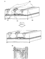
Another embodiment of the present invention will be described with reference to FIG. FIG. 4A is a perspective view when FIG. 4B is cut along AA ′. Note that the ratios such as the membrane pressure in this drawing are changed for the sake of clarity, and may be different from the actual ratios. In addition, there is a part where the description is omitted.
本実施の形態では、TFTを作製して層間絶縁膜などを作製し、コンタクトホールを開けた後、配線のパターンに沿って隔壁401を形成する。隔壁401は液滴吐出法を用いて材料を滴下して作製するとよいが、それに限ることでは無い。また、材料としては、リフローの熱に耐えることができ隔壁の役割を果たす絶縁物よい。また、この隔壁401はリフロー後、選択的に除去が可能な材料であり、除去することが前提であれば絶縁物で無くともよい。これら材料は使用者が適宜選択することが可能である。この隔壁作製の工程はコンタクトホールを開ける前に形成してもよい。
In this embodiment mode, a TFT is manufactured to form an interlayer insulating film and the like, a contact hole is formed, and then a
続いて、液滴吐出法により導電性組成物の分散した液滴を、隔壁の内側に滴下し、402に代表されるような配線を形成する。配線は前述してきたとおり、コンタクトホールの形状を反映し凹部403が形成される。また、場所によっては404の様にコンタクトホールが完全に充填されず、コンタクト不良を起こす場合もある。
Subsequently, a droplet in which the conductive composition is dispersed is dropped inside the partition wall by a droplet discharge method to form a wiring as represented by 402. As described above, the
液滴吐出法により液滴を配線のパターンに沿って形成したら、配線を構成している導電性組成物の軟化点以上の温度に加熱処理を行ってリフローする。 When the droplets are formed along the wiring pattern by the droplet discharge method, heat treatment is performed at a temperature equal to or higher than the softening point of the conductive composition constituting the wiring and reflowing is performed.
結果、凹部の凹凸は緩和され、配線表面は平坦化し、コンタクトホールが充填されることでコンタクト不良はリペアされこれら起因の不都合が解消される。これによって飛躍的に信頼性が向上することとなる。また、隔壁が設けられていることでリフローされた配線が不都合な部分に広がり、ショートしてしまうことも防止でき精密なパターンを形成する際にも信頼性を損なうことが無い。もちろん、これらの工程は液滴吐出法を使用しているため材料の無駄が少なくコスト的にも非常に優秀な方法である。また、必要な部分のみの加工であるため大面積基板であっても迅速に処理を行うことが可能である。 As a result, the unevenness of the recesses is relaxed, the surface of the wiring is flattened, and the contact holes are filled to repair the contact failure and the disadvantages due to these are eliminated. This dramatically improves the reliability. In addition, the provision of the partition wall prevents the reflowed wiring from spreading to an inconvenient portion and causing a short circuit, and does not impair reliability when forming a precise pattern. Of course, since these steps use the droplet discharge method, the material is not wasted and the method is very excellent in terms of cost. In addition, since only necessary portions are processed, even a large area substrate can be processed quickly.
本実施の形態には表示装置の画素部を例にとって説明したが、もちろんそれに限らず駆動回路部においても、CPUを代表とする集積回路にも適用することが可能である。 In this embodiment mode, the pixel portion of the display device is described as an example. However, the present invention is not limited to this, and the present invention can also be applied to a driver circuit portion and an integrated circuit typified by a CPU.
また、本実施の形態は図18に示したように隔壁の代わりに溝1401を設けることによっても実現が可能である。
Further, this embodiment can also be realized by providing a
本発明の実施の一例として、アクティブマトリクス型液晶表示装置の作成方法を図5,6により詳細に説明する。本実施例では従来使用していたフォトリソグラフィ法によるパターニングを用いていないが、適宜前述した実施の形態3〜4と組み合わせることによって、より信頼性の向上した液晶表示装置を提供することができるようになる。また、必要に応じて従来のプロセスを使用することは使用者の判断にゆだねるところである。 As an example of the embodiment of the present invention, a method for producing an active matrix liquid crystal display device will be described in detail with reference to FIGS. In this embodiment, patterning by a photolithography method that has been conventionally used is not used, but a liquid crystal display device with higher reliability can be provided by appropriately combining with the above-described third to fourth embodiments. become. Also, the use of conventional processes as needed is at the discretion of the user.
ここでは、本発明を用いて、アクティブマトリクス液晶表示装置のうち、Nチャネル型TFT(スイッチ用)と容量を同一基板上に形成する作製工程について説明する。 Here, a manufacturing process in which an N-channel TFT (for a switch) and a capacitor are formed over the same substrate in an active matrix liquid crystal display device using the present invention will be described.
基板601には、ガラス基板、プラスチック基板に代表される可撓性基板など、本工程の処理温度に耐えうる基板を用いる(図5(A))。具体的には、透光性を有する基板601を用いてアクティブマトリクス基板を作製する。基板サイズとしては、600mm×720mm、680mm×880mm、1000mm×1200mm、1100mm×1250mm、1150mm×1300mm、1500mm×1800mm、1800mm×2000mm、2000mm×2100mm、2200mm×2600mm、または2600mm×3100mmのような大面積基板を用い、製造コストを削減することが好ましい。用いることのできる基板として、コーニング社の#7059ガラスや#1737ガラスなどに代表されるバリウムホウケイ酸ガラスやアルミノホウケイ酸ガラスなどのガラス基板を用いることができる。更に他の基板として、石英基板、プラスチック基板などの透光性基板を用いることもできる。
As the
本実施例ではガラス基板601を用いた。続いて基板601上に、絶縁膜から成る下地膜602を形成する。下地膜602は単層又は積層構造のいずれでもよく、本実施例では、2層構造として、スパッタリング法を用い、1層目として窒化酸化珪素膜を50nm、2層目として酸化窒化珪素膜を50nmの厚さに形成し、その後CMP法などの方法により表面を平坦化した(図5(A))。
In this embodiment, a
次いで、下地膜602上に半導体層603を形成する。半導体層603は、まず公知の方法(スパッタリング法、LPCVD法、プラズマCVD法等)により25〜80nmの厚さで半導体膜を成膜する。次いで前記半導体膜を公知の結晶化法(レーザー結晶化法、RTA又はファーネスアニール炉を用いる熱結晶化法、結晶化を助長する金属元素を用いる熱結晶化法等)を用いて結晶化させる。なお前記半導体膜としては、非晶質半導体膜、微結晶半導体膜、結晶質半導体膜又は非晶質珪素ゲルマニウム膜などの非晶質構造を有する化合物半導体膜などを用いても良い。
Next, a
本実施例では、プラズマCVD法を用いて、膜厚50nmの非晶質珪素膜を成膜した。その後、ニッケルを含む溶液を非晶質珪素膜上に保持させ、この非晶質珪素膜に脱水素化(500℃、1時間)を行った後、熱結晶化(550℃、4時間)を行って結晶質珪素膜を形成した。その後、本発明による液滴吐出法によって、インクジェットノズル604より吐出したレジスト605によりマスクパターンを形成した。さらに、該マスクパターンを使用してドライエッチング法により半導体層603を形成した(図5(B))。
In this example, an amorphous silicon film having a thickness of 50 nm was formed by plasma CVD. Thereafter, a solution containing nickel is held on the amorphous silicon film, and after dehydrogenation (500 ° C., 1 hour) is performed on the amorphous silicon film, thermal crystallization (550 ° C., 4 hours) is performed. A crystalline silicon film was formed. Thereafter, a mask pattern was formed from the resist 605 discharged from the
なお、レーザー結晶化法で結晶質半導体膜を作製する場合のレーザーは、連続発振またはパルス発振の気体レーザー又は固体レーザーを用いれば良い。前者の気体レーザーとしては、エキシマレーザー、YAGレーザー等が挙げられ、後者の固体レーザーとしては、Cr、Nd等がドーピングされたYAG、YVO4等の結晶を使ったレーザー等が挙げられる。なお非晶質半導体膜の結晶化に際し、大粒径に結晶を得るためには、連続発振が可能な固体レーザーを用い、基本波の第2〜第4高調波を適用するのが好ましい。上記レーザーを用いる場合には、レーザー発振器から放射されたレーザービームを光学系で線状に集光して、半導体膜に照射すると良い。 Note that as a laser for forming a crystalline semiconductor film by a laser crystallization method, a continuous wave or pulsed gas laser or solid laser may be used. Examples of the former gas laser include an excimer laser and a YAG laser, and examples of the latter solid laser include a laser using a crystal such as YAG or YVO 4 doped with Cr, Nd, or the like. In order to obtain a crystal with a large grain size when the amorphous semiconductor film is crystallized, it is preferable to use a solid-state laser capable of continuous oscillation and apply the second to fourth harmonics of the fundamental wave. In the case of using the above laser, the laser beam emitted from the laser oscillator may be condensed linearly by an optical system and irradiated onto the semiconductor film.
但し、本実施例では、結晶化を助長する金属元素を用いて非晶質珪素膜の結晶化を行ったため、前記金属元素が結晶質珪素膜中に残留している。そのため、前記結晶質珪素膜上に50〜100nmの非晶質珪素膜を形成し、加熱処理(RTA法、ファーネスアニール炉を用いた熱アニール等)を行って、該非晶質珪素膜中に前記金属元素を拡散させ、前記非晶質珪素膜は加熱処理後にエッチングを行って除去する。その結果、前記結晶質珪素膜中の金属元素の含有量を低減または除去することができる。また半導体層603を形成後、TFTのしきい値を制御するために微量な不純物元素(ボロン)のドーピング(チャネルドーピング)を行ってもよい。
However, in this embodiment, since the amorphous silicon film was crystallized using a metal element that promotes crystallization, the metal element remains in the crystalline silicon film. Therefore, an amorphous silicon film having a thickness of 50 to 100 nm is formed on the crystalline silicon film, and heat treatment (RTA method, thermal annealing using a furnace annealing furnace, etc.) is performed, and the amorphous silicon film Metal elements are diffused, and the amorphous silicon film is removed by etching after the heat treatment. As a result, the content of the metal element in the crystalline silicon film can be reduced or removed. In addition, after forming the
次いで、半導体層603を覆うゲート絶縁膜606を形成する。ゲート絶縁膜606はプラズマCVD法やスパッタ法を用いて、膜厚を40〜150nmとして珪素を含む絶縁膜で形成する。本実施例では、ゲート絶縁膜606としてプラズマCVD法により酸化窒化珪素膜を115nmの厚さに形成した。
Next, a
さらに、同様に液滴吐出法により、減圧又は真空中で第1の導電層(ゲート配線、ゲート電極、キャパシタ電極)608を形成する(図5(C))。 Further, similarly, a first conductive layer (gate wiring, gate electrode, capacitor electrode) 608 is formed under reduced pressure or in vacuum by a droplet discharge method (FIG. 5C).
インクジェットには多数の液滴噴射ノズルを有している。また、ノズル径の異なるインクヘッドを複数用意し、用途に応じて、ノズル径の異なるインクヘッドを使い分けてもよい。なお、通常のインクヘッドのノズル径は50〜100μmであり、このノズル径にも依存するが、スループットを考慮して、一度の走査で形成できるようにするために、一行又は一列と同じ長さになるように、複数のノズルを並列に配置してもよい。また、任意の個数のノズルを配置して、複数回走査しても構わないし、また同じ箇所を複数回走査することで重ね塗りをしてもよい。さらに、インクヘッドを走査することが好ましいが、基板を移動させても構わない。なお基板とインクヘッドとの距離は、所望の箇所に滴下するために、できるだけ近づけておくことが好ましく、具体的には、0.1〜2ミリ程度が好ましい。 An ink jet has a large number of droplet ejection nozzles. Alternatively, a plurality of ink heads having different nozzle diameters may be prepared, and ink heads having different nozzle diameters may be used properly according to the application. In addition, the nozzle diameter of a normal ink head is 50 to 100 μm and depends on the nozzle diameter, but considering the throughput, in order to be able to form by one scanning, the same length as one row or one column A plurality of nozzles may be arranged in parallel so that Further, an arbitrary number of nozzles may be arranged and scanned a plurality of times, or the same portion may be scanned a plurality of times and overcoated. Furthermore, although it is preferable to scan the ink head, the substrate may be moved. The distance between the substrate and the ink head is preferably as close as possible so as to be dropped at a desired location, and specifically, about 0.1 to 2 mm is preferable.
インクヘッドから1回に吐出する組成物の量は10〜70pl、粘度は100cp以下、粒径0.1μm以下が好ましい。これは、乾燥が起こることを防ぎ、また粘度が高すぎると、吐出口から組成物を円滑に吐出できなくなったりするためである。用いる溶媒や、用途に合わせて組成物の粘度、表面張力、乾燥速度などは適宜調節する。またインクヘッドから吐出される組成物は、基板上で連続して滴下して線状又はストライプ状に形成することが好ましい。しかし、例えば1ドット毎などの所定の箇所毎に滴下してもよい。 The amount of the composition ejected from the ink head at one time is preferably 10 to 70 pl, the viscosity is 100 cp or less, and the particle size is 0.1 μm or less. This is because drying is prevented and the composition cannot be smoothly discharged from the discharge port if the viscosity is too high. The viscosity, surface tension, drying rate and the like of the composition are adjusted as appropriate according to the solvent used and the application. Moreover, it is preferable that the composition discharged from the ink head is continuously dropped on the substrate to form a linear shape or a stripe shape. However, it may be dropped at predetermined locations such as every dot.
インクヘッドから吐出する組成物は、タンタル(Ta)、タングステン(W)、チタン(Ti)、モリブデン(Mo)、アルミニウム(Al)、銀(Ag)、銅(Cu)、クロム(Cr)、ニオブ(Nd)から選択された元素、または前記元素を主成分とする合金材料若しくは化合物材料、AgPdCu合金などのAg合金、もしくはAl合金から適宜選択された導電性の材料を溶媒に溶解又は分散させたものを用いる。溶媒には、酢酸ブチル、酢酸エチル等のエステル類、イソプロピルアルコール、エチルアルコール等のアルコール類、メチルエチルケトン、アセトン等の有機溶剤などを用いる。溶媒の濃度は、導電性材料の種類などに適宜決定するとよい。 The composition ejected from the ink head is tantalum (Ta), tungsten (W), titanium (Ti), molybdenum (Mo), aluminum (Al), silver (Ag), copper (Cu), chromium (Cr), niobium. An element selected from (Nd) or an alloy material or compound material containing the element as a main component, an Ag alloy such as an AgPdCu alloy, or a conductive material appropriately selected from an Al alloy was dissolved or dispersed in a solvent. Use things. As the solvent, esters such as butyl acetate and ethyl acetate, alcohols such as isopropyl alcohol and ethyl alcohol, and organic solvents such as methyl ethyl ketone and acetone are used. The concentration of the solvent may be appropriately determined depending on the type of conductive material.
また、インクヘッドから吐出する組成物として、銀(Ag)、金(Au)、白金(Pt)を粒径10nm以下で分散させた超微粒子(ナノメタル粒子)を用いてもよい。このように、粒径の微細な粒子を溶媒に分散又は溶解した組成物を用いると、ノズルの目詰まりという問題を解決することができる。なお、液滴吐出法を用いる本発明では、組成物の構成材料の粒径は、ノズルの粒径よりも小さいことが必要となる。また、ポリエチレンジオキシチオフェン/ポリスチレンスルホン酸(PEDT/PSS)水溶液などの導電性ポリマー(導電性高分子)を用いてもよい。 Further, as a composition ejected from the ink head, ultrafine particles (nanometal particles) in which silver (Ag), gold (Au), and platinum (Pt) are dispersed with a particle diameter of 10 nm or less may be used. As described above, when a composition in which fine particles having a small particle size are dispersed or dissolved in a solvent is used, the problem of nozzle clogging can be solved. In the present invention using a droplet discharge method, the particle size of the constituent material of the composition needs to be smaller than the particle size of the nozzle. Alternatively, a conductive polymer (conductive polymer) such as a polyethylenedioxythiophene / polystyrene sulfonic acid (PEDT / PSS) aqueous solution may be used.
また、銀または銅といった低抵抗金属を配線材料として用いると、配線抵抗の低抵抗化を図ることができるため、大型の基板を用いる場合に好ましい。しかも、これらの金属材料は通常のドライエッチング法によって加工することが難しいため、液滴吐出法で直接パターニングを行うことは、極めて効果的である。但し、例えば銅などの場合には、トランジスタの電気的特性に悪影響を及ぼさないようにするために、拡散を防ぐバリア性の導電膜を設けることが好ましい。バリア性の導電膜により、トランジスタが有する半導体に銅が拡散することなく、配線を形成することができる。このバリア性の導電膜としては、窒化タンタル(TaN)、窒化チタン(TiN)又は窒化タングステン(WN)から選ばれた一種又は複数種の積層膜を用いることができる。また、銅は酸化しやすいため、酸化防止剤などを併用することが好ましい。 In addition, when a low-resistance metal such as silver or copper is used as a wiring material, the wiring resistance can be reduced, which is preferable when a large substrate is used. Moreover, since it is difficult to process these metal materials by a normal dry etching method, it is very effective to perform patterning directly by a droplet discharge method. However, in the case of copper, for example, it is preferable to provide a barrier conductive film that prevents diffusion in order not to adversely affect the electrical characteristics of the transistor. With the barrier conductive film, a wiring can be formed without diffusion of copper into a semiconductor included in the transistor. As the barrier conductive film, one or more kinds of laminated films selected from tantalum nitride (TaN), titanium nitride (TiN), and tungsten nitride (WN) can be used. Moreover, since copper is easily oxidized, it is preferable to use an antioxidant together.
その後、第1の導電層が形成された基板に常圧または減圧、あるいは真空中で、150〜300度の範囲で加熱処理を施すことで、その溶媒を揮発させて、その組成物密度を向上させて、抵抗値が低くなるようにする。但し、インクジェットノズル604から吐出する組成物における溶媒は、基板に滴下後に揮発するものが適している。本実施例の様に真空下で吐出が行われている場合は、通常の大気圧下の場合に比べて、蒸発速度が早いのが特徴であるが、特にトルエンなどの揮発性の高い溶媒を用いると、組成物を基板に滴下後、瞬時に揮発する。そのような場合には、加熱処理の工程は削除しても構わない。しかし、組成物の溶媒は特に限定されず、滴下後に揮発する溶媒を用いた場合であっても、加熱処理を施すことで、その組成物密度を向上させて、所望の抵抗値になるようにしてもよい。またこの加熱処理は、液滴吐出法により薄膜を形成した毎に行ってもよいし、任意の工程毎に行ってもよいし、全ての工程が終了した後に一括して行ってもよい。また、リフローを行う場合には省略しもかまわない。
Thereafter, the substrate on which the first conductive layer is formed is subjected to heat treatment in the range of 150 to 300 degrees at normal pressure, reduced pressure, or vacuum, thereby volatilizing the solvent and improving the composition density. To reduce the resistance value. However, as the solvent in the composition discharged from the
加熱処理は、加熱源にハロゲンなどのランプを用いて、直接基板を高速加熱するランプアニール装置や、レーザー光を照射するレーザー照射装置を用いる。両者とも加熱源を走査することで、所望の箇所のみに加熱処理を施すことができる。その他の方法として、所定の温度に設定されたファーネスアニールを用いてもよい。但し、ランプを用いる場合には、加熱処理を行う薄膜の組成を破壊せず、加熱のみを可能とする波長の光であり、例えば、400nmよりも波長の長い光、即ち赤外光以上の波長の光が好ましい。取り扱いの面からは、遠赤外線(代表的な波長は4〜25μm)を用いることが好ましい。またレーザー光を用いる場合、レーザー発振装置から発振されるレーザー光の基板におけるビームスポットの形状は、列又は行の長さと同じ長さになるように線状に成形することが好ましい。そうすると、一度の走査でレーザー照射を終了させることができる。本実施例では、加熱処理として、通常のファーネスアニールを用いた。 The heat treatment uses a lamp annealing apparatus that directly heats the substrate at high speed using a lamp such as halogen as a heating source, or a laser irradiation apparatus that irradiates laser light. In both cases, the heat treatment can be performed only on a desired portion by scanning the heat source. As another method, furnace annealing set to a predetermined temperature may be used. However, in the case of using a lamp, it is light having a wavelength that enables heating only without destroying the composition of the thin film to be heat-treated, for example, light having a wavelength longer than 400 nm, that is, a wavelength longer than infrared light Are preferred. From the viewpoint of handling, it is preferable to use far infrared rays (typical wavelength is 4 to 25 μm). In the case of using laser light, the shape of the beam spot on the substrate of the laser light oscillated from the laser oscillation device is preferably linearly formed so as to have the same length as the column or row. If it does so, laser irradiation can be completed by one scan. In this example, normal furnace annealing was used as the heat treatment.
続いて、ゲート電極608をマスクとして、半導体層603に、N型又はP型を付与する不純物元素を添加するドーピング処理を行う。本実施例では、半導体層603にN型を付与する不純物元素を添加し、半導体層603にP型を付与する不純物元素を添加して、不純物領域を形成した。同時に、不純物元素が全く添加されない領域又は微量の不純物元素が添加された領域(チャネル形成領域と総称)を形成した。
Subsequently, doping treatment for adding an impurity element imparting N-type or P-type to the
この後、一旦全面を覆う第1の層間絶縁膜609を形成する。該第1の層間絶縁膜609はプラズマCVD法やスパッタ法を用いて、膜厚を40〜150nmとして珪素を含む絶縁膜で形成する。本実施例では、第1の層間絶縁膜609としてプラズマCVD法により窒化珪素膜を100nmの厚さに形成した。さらに、同様にして全面を覆う第2の層間絶縁膜610を形成する。第2の層間絶縁膜610としては、CVD法によって形成された酸化珪素膜、SOG(Spin On Glass)法又はスピンコート法によって塗布された酸化珪素膜、アクリル等の有機絶縁膜又は非感光性の有機絶縁膜が0.7〜5μmの厚さで形成する。本実施例では、塗布法で膜厚1.6μmのアクリル膜50を形成した。なお第2の層間絶縁膜610は、基板601上に形成されたTFTによる凹凸を緩和し、平坦化する意味合いが強いので、平坦性に優れた膜が好ましい。さらに、第3の層間絶縁膜611となる窒化珪素膜を0.1μmの厚さで形成する。
Thereafter, a first
しかる後に、コンタクトホール613を形成するためのレジストパターン612を、上述の場合と同様に液滴吐出法によって形成する。ついで、該レジストパターンをマスクとして異方性ドライエッチング法によってコンタクトホール613を形成した(図5(D))。
Thereafter, a resist
このコンタクトホールの形成は、上記の様にレジストを塗布することによって形成してもよいが、他の方法として図12の様にインクジェット装置のノズル505からエッチング液506を滴下することによって層間絶縁膜503をエッチングし、コンタクトホールを形成してもよい。コンタクトホールが形成されたら下層の配線または導電層504へのダメージを最小限に抑えるためにインクジェットのノズルを換えて洗浄液508を滴下するなどし、洗浄するとよい。
This contact hole may be formed by applying a resist as described above. Alternatively, an interlayer insulating film may be formed by dropping an
この後、レジストパターン612を除去した後、液滴吐出法により、第2の導電層(ソース配線、ドレイン配線)615を前記コンタクトホール613の底部まで延在するように形成する。本実施例において、吐出する組成物はとしては、銀とアルミニウムの合金の微粒子を分散剤を用いて有機溶媒中に分散させた液を用いた。銀とアルミニウムの比率は銀に対しアルミニウムが40〜80atom%程度のものを使用するとよい。他にアルミニウム単体、アルミニウムとゲルマニウムの合金、銀とゲルマニウムの合金や銀と錫の合金等の材料を使用することが可能である。材料については使用者が適宜選択することが可能である。このときの断面図を図6(A)に示す。
Thereafter, after removing the resist
この場合、コンタクトホールの底部には、Alで形成されたゲート電極パターンあるいはSiパターン上のソース/ドレイン領域が露出している。コンタクトホール内には、十分の液滴を与える必要が有るため、この部分に対してより多くの液滴の吐出を行うことが必要である。あるいは、重ね塗りにより、この部分の塗布量を増すことも、コンタクト抵抗不良を抑制する点で重要となる。なお、第2の導電層を形成する場合には、吐出する組成物の粘度を最適な値に設定することが必要である。 In this case, the source / drain region on the gate electrode pattern or Si pattern formed of Al is exposed at the bottom of the contact hole. Since it is necessary to give enough droplets in the contact hole, it is necessary to discharge more droplets to this portion. Alternatively, increasing the coating amount of this portion by overcoating is also important in terms of suppressing contact resistance defects. When forming the second conductive layer, it is necessary to set the viscosity of the composition to be discharged to an optimum value.
引き続いて、加熱処理を行う。加熱処理はRTA、GRTA法、レーザ照射、ランプ加熱などにより行うとよい。本実施例ではAgとAlの合金で配線を作製しているため500〜600℃で瞬間的に加熱を行うことによってリフローする。(図6(B))これにより、コンタクトホールの形状を反映した凹凸や乾燥課程によって発生した配線形状の差異が緩和される。また、コンタクトホールへの組成物の充填が不十分であったとしてもリペアが可能である。ここまでの工程により、絶縁表面を有する基板601上にトランジスタを形成することができた。
Subsequently, heat treatment is performed. The heat treatment may be performed by RTA, GRTA method, laser irradiation, lamp heating, or the like. In this embodiment, since the wiring is made of an alloy of Ag and Al, reflow is performed by instantaneously heating at 500 to 600 ° C. (FIG. 6B) Thereby, the unevenness reflecting the shape of the contact hole and the difference in the wiring shape caused by the drying process are alleviated. Further, even if the contact hole is not sufficiently filled with the composition, repair is possible. Through the above steps, a transistor can be formed over the
続いて、全面に第2の導電層615と電気的に接続されるように、透明導電体からなる画素電極616を形成する(図6(B))。画素電極616には、一例として、酸化インジウムと酸化スズの化合物(ITO)、酸化インジウムと酸化亜鉛の化合物、酸化亜鉛、酸化スズ、酸化インジウム、窒化チタンなどが挙げられる。本実施例では画素電極616として、液滴吐出法で、0.1μmの厚さでITO膜を形成した(図6(C))。
Subsequently, a
以上、画素部においてはソース配線と、画素部のTFT及び保持容量と、端子部で構成されたアクティブマトリクス基板を作製することができる。そして、必要があれば、アクティブマトリクス基板または対向基板を所望の形状に分断する。
この後、共通電極617、カラーフィルタ618、ブラックマトリックス619などが形成された対向基板620と貼り合わせる。そして所定の方法で液晶621を注入し、液晶表示装置を完成する。(図6(D))。
As described above, an active matrix substrate including a source wiring, a TFT and a storage capacitor of the pixel portion, and a terminal portion can be manufactured in the pixel portion. If necessary, the active matrix substrate or the counter substrate is divided into a desired shape.
After that, it is bonded to the
以上の工程によって得られた液晶モジュールに、バックライト、導光板を設け、カバーで覆えば、アクティブマトリクス型液晶表示装置(透過型)が完成する。なお、カバーと液晶モジュールは接着剤や有機樹脂を用いて固定する。また、透過型であるので偏光板は、アクティブマトリクス基板と対向基板の両方に貼り付ける。 An active matrix liquid crystal display device (transmission type) is completed when a backlight and a light guide plate are provided on the liquid crystal module obtained by the above steps and covered with a cover. The cover and the liquid crystal module are fixed using an adhesive or an organic resin. Further, since it is a transmissive type, the polarizing plate is attached to both the active matrix substrate and the counter substrate.
また、本実施の形態は透過型の例を示したが、特に限定されず、反射型や半透過型の液晶表示装置も作製することができる。反射型の液晶表示装置を得る場合は、画素電極として光反射率の高い金属膜、代表的にはアルミニウムまたは銀を主成分とする材料膜、またはそれらの積層膜等を用いればよい。 Although this embodiment mode shows a transmissive type example, there is no particular limitation, and a reflective or transflective liquid crystal display device can also be manufactured. In the case of obtaining a reflective liquid crystal display device, a metal film with high light reflectivity, typically a material film containing aluminum or silver as a main component, or a laminated film thereof may be used as the pixel electrode.
また、必要に応じて駆動回路部など高度な集積が必要な部分において、実施の形態3や実施の形態4と組み合わせて配線を作製するとより信頼性が向上する。もちろん部分的にだけではなく全面に適用してもよい。 Further, when a wiring is manufactured in combination with the third embodiment or the fourth embodiment in a portion where a high degree of integration is necessary, such as a drive circuit portion, reliability is further improved. Of course, you may apply not only to a part but to the whole surface.
以上、本発明の第1の実施例について、アクティブマトリックス型の液晶表示装置について説明したが、本実施実施例に限定されることなく、本発明の趣旨に基づき適用が可能となる。例えばアクティブマトリクス型有機EL表示装置の場合についても同様に適用することが可能である。また、本実施例で取り上げた材料、形成方法に関しても、本発明の趣旨に則り適宜選択して用いることが可能である。 As described above, the active matrix type liquid crystal display device has been described with respect to the first embodiment of the present invention. However, the present invention is not limited to this embodiment, and can be applied based on the gist of the present invention. For example, the present invention can be similarly applied to an active matrix organic EL display device. Further, the materials and forming methods taken up in this embodiment can be appropriately selected and used in accordance with the gist of the present invention.
本発明の第二の実施例について、図7、8を用いて詳細に説明する。本発明においても、従来使用していたフォトリソグラフィ法によるパターニングを用いていないが、適宜前述した実施の形態3〜4と組み合わせることによって、より信頼性の向上した液晶表示装置を提供することができるようになる。また、必要に応じて従来のプロセスを使用することは使用者の判断にゆだねるところである。 A second embodiment of the present invention will be described in detail with reference to FIGS. Also in the present invention, the patterning by the photolithography method that has been conventionally used is not used, but a liquid crystal display device with improved reliability can be provided by appropriately combining with the above-described third to fourth embodiments. It becomes like this. Also, the use of conventional processes as needed is at the discretion of the user.
基板801には、ガラス基板、プラスチック基板に代表される可撓性基板など、本工程の処理温度に耐えうる基板を用いる(図8(A))。本実施例ではガラス基板801を用いた。続いて基板801上に、絶縁膜から成る下地膜802を形成する。下地膜802は単層又は積層構造のいずれでもよく、本実施例では、2層構造として、スパッタリング法を用い、1層目として窒化酸化珪素膜を50nm、2層目として酸化窒化珪素膜を50nmの厚さに形成し、その後CMP法などの方法により表面を平坦化した(図7(A))。
As the
次いで、下地膜802上に半導体層803を形成する。半導体層803は、まず公知の方法(スパッタリング法、LPCVD法、プラズマCVD法等)により25〜80nmの厚さで半導体膜を成膜する。次いで前記半導体膜を公知の結晶化法(レーザー結晶化法、RTA又はファーネスアニール炉を用いる熱結晶化法、結晶化を助長する金属元素を用いる熱結晶化法等)を用いて結晶化させる。なお前記半導体膜としては、非晶質半導体膜、微結晶半導体膜、結晶質半導体膜又は非晶質珪素ゲルマニウム膜などの非晶質構造を有する化合物半導体膜などを用いても良い。
Next, a
本実施例では第一の実施例と同様にして、プラズマCVD法を用いて、膜厚50nmの非晶質珪素膜を成膜した。その後、ニッケルを含む溶液を非晶質珪素膜上に保持させ、この非晶質珪素膜に脱水素化(500℃、1時間)を行った後、熱結晶化(550℃、4時間)を行って結晶質珪素膜を形成した。その後、減圧又は真空中でインクジェットヘッド807より吐出したレジストのパターニングを行い、該レジストパターンをマスクレジストのパターニングを行い、該レジストパターンをマスクとしてドライエッチング法によって半導体層804〜806を形成した(図7(B))
In this example, similarly to the first example, an amorphous silicon film having a thickness of 50 nm was formed by plasma CVD. Thereafter, a solution containing nickel is held on the amorphous silicon film, and after dehydrogenation (500 ° C., 1 hour) is performed on the amorphous silicon film, thermal crystallization (550 ° C., 4 hours) is performed. A crystalline silicon film was formed. After that, the resist discharged from the
続いて、ゲート絶縁膜809を形成する。ゲート絶縁膜809はプラズマCVD法により酸化窒化珪素膜を115nmの厚さに形成した(図7(B))。
Subsequently, a
ついで、第一の実施例と同様にして、減圧又は真空中で第1の導電層(ゲート配線、ゲート電極)810〜813をタングステン膜で形成する。(図7(B)) Next, in the same manner as in the first embodiment, first conductive layers (gate wirings, gate electrodes) 810 to 813 are formed of tungsten films in a reduced pressure or vacuum. (Fig. 7 (B))
その後、第1の導電層が形成された基板に常圧または減圧、あるいは真空中で、150〜300度の範囲で加熱処理を施すことで、その溶媒を揮発させ良好な導電特性を得る。但し、インクヘッド807から吐出する組成物における溶媒は、基板に滴下後に揮発するものが適している。特にトルエンなどの揮発性の高い溶媒を用いると、組成物を基板に滴下後、揮発する。そのような場合には、加熱処理の工程は削除しても構わない。しかし、組成物の溶媒は特に限定されず、滴下後に揮発する溶媒を用いた場合であっても、加熱処理を施すことで、その組成物の粘度を低下させて、所望の粘度になるようにしてもよい。またこの加熱処理は、液滴吐出法により薄膜を形成した毎に行ってもよいし、任意の工程毎に行ってもよいし、全ての工程が終了した後に一括して行ってもよい。また、リフローを行う場合省略してもかまわない。
Thereafter, the substrate on which the first conductive layer is formed is subjected to heat treatment in the range of 150 to 300 degrees under normal pressure, reduced pressure, or vacuum, whereby the solvent is volatilized to obtain good conductive characteristics. However, as the solvent in the composition discharged from the
さらに、ゲート電極811〜813をマスクとして、半導体層804〜806に、N型又はP型を付与する不純物元素を添加するドーピング処理を行う。本実施例では、半導体層804にN型を付与する不純物元素を添加し、半導体層805、806にP型を付与する不純物元素を添加して、不純物領域を形成した。同時に、不純物元素が全く添加されない領域又は微量の不純物元素が添加された領域(チャネル形成領域と総称)を形成した。
Further, doping treatment for adding an impurity element imparting N-type or P-type to the semiconductor layers 804 to 806 is performed using the
この後、一旦全面を覆う第1の層間絶縁膜814を形成する。該第1の層間絶縁膜814はプラズマCVD法やスパッタ法を用いて、膜厚を40〜150nmとして珪素を含む絶縁膜で形成する。本実施例では、第1の層間絶縁膜814としてプラズマCVD法により窒化珪素膜を100nmの厚さに形成した。さらに、同様にして全面を覆う第2の層間絶縁膜815を形成する。第2の層間絶縁膜815としては、塗布法で膜厚1.6μmのアクリル膜を形成した。さらに、第3の層間絶縁膜816となる窒化珪素膜を0.1μmの厚さで形成する。
Thereafter, a first
しかる後に、コンタクトホールを形成するためのレジストパターンを、上述の場合と同様に液滴吐出法によって形成する。ついで、該レジストパターンをマスクとして異方性ドライエッチング法によってコンタクトホールを形成した。(図7(C)) Thereafter, a resist pattern for forming a contact hole is formed by a droplet discharge method in the same manner as described above. Next, contact holes were formed by anisotropic dry etching using the resist pattern as a mask. (Fig. 7 (C))
この後、第2の導電層(ソース配線、ドレイン配線)817〜822を前記コンタクトホールの底部まで延在するように形成する。本実施例においては、第2の導電層は銀と錫の微粒子を界面活性剤を用いて有機溶媒中に分散させた液を吐出して配線パターンを形成した。銀とアルミニウムの比率は銀に対しアルミニウムが40〜80atom%程度のものを使用するとよい。他にアルミニウム単体、アルミニウムとゲルマニウムの合金、銀とゲルマニウムの合金や銀と錫の合金等の材料を使用することが可能である。材料については使用者が適宜選択することが可能である。 Thereafter, second conductive layers (source wiring and drain wiring) 817 to 822 are formed so as to extend to the bottom of the contact hole. In this example, the second conductive layer was formed by discharging a liquid in which fine particles of silver and tin were dispersed in an organic solvent using a surfactant to form a wiring pattern. The ratio of silver to aluminum is preferably about 40 to 80 atom% of aluminum with respect to silver. In addition, it is possible to use a material such as aluminum alone, an alloy of aluminum and germanium, an alloy of silver and germanium, or an alloy of silver and tin. The material can be appropriately selected by the user.
このようにして形成された配線パターンにはコンタクトホールなどを反映して凹凸が形成されていたり、有機溶媒の乾燥状況によって形状に差異が生じてしまっていたり、完全にコンタクトホールが充填されていなかったりなどの不都合が発生している可能性がある。 The wiring pattern formed in this way has irregularities reflecting the contact holes, etc., the shape varies depending on the drying condition of the organic solvent, or the contact holes are not completely filled There is a possibility that inconvenience has occurred.
この不都合を解消するために、引き続いて加熱処理を行う。加熱処理はRTA、GRTA法、レーザ照射、ランプ加熱などにより行うとよい。本実施例ではAgとAlの合金で配線を作製しているため500〜600℃で瞬間的に加熱を行うことによってリフローする。これにより、コンタクトホールの形状を反映した凹凸や乾燥課程によって発生した配線形状の差異が緩和される。また、コンタクトホールへの組成物の充填が不十分であったとしてもリペアが可能である。ここまでの工程により、絶縁表面を有する基板801上にトランジスタを形成することができた。このときの断面図を図7(D)に示す。
In order to eliminate this inconvenience, heat treatment is subsequently performed. The heat treatment may be performed by RTA, GRTA method, laser irradiation, lamp heating, or the like. In this embodiment, since the wiring is made of an alloy of Ag and Al, reflow is performed by instantaneously heating at 500 to 600 ° C. Thereby, the unevenness reflecting the shape of the contact hole and the difference in wiring shape caused by the drying process are alleviated. Further, even if the contact hole is not sufficiently filled with the composition, repair is possible. Through the above steps, a transistor can be formed over the
続いて、全面に第2の導電層820、822と電気的に接続されるように、透明導電体からなる画素電極901、902を形成する。画素電極901、902には、一例として、酸化インジウムと酸化スズの化合物(ITO)、酸化インジウムと酸化亜鉛の化合物、酸化亜鉛、酸化スズ、酸化インジウム、窒化チタンなどが挙げられる。本実施例では画素電極901、902として、液滴吐出法を使用して、0.1μmの厚さでITO膜を形成した(図8(A))。
Subsequently,
この後、有機ELによる発光素子の形成工程に入ることになる。画素電極901、902の端面を覆うように絶縁膜903を形成する。絶縁膜903を形成する材料は特に限定されず、無機又は有機の材料で形成することができる。この後、発光層となる有機ELを含む領域を形成することになるが、画素電極901、902と接するように発光層904、905を減圧又は真空中で順次形成する(図8(B、C))。発光層904、905の材料は特に限定されるものではないが、カラー表示を行う場合には、赤、緑、青の各色の材料を用いる。ついで、第2の画素電極(陰極)906を減圧又は真空中で蒸着法により形成する(図8(D))。
Thereafter, a process of forming a light emitting element by organic EL is started. An insulating
第2の画素電極(陰極)906は、仕事関数の小さい金属(リチウム(Li)、マグネシウム(Mg)、セシウム(Cs))を含む薄膜、Li、Mg等を含む薄膜上に積層した透明導電膜との積層膜で形成する。膜厚は陰極として作用するように適宜設定すればよいが、0.01〜1μm程度の厚さで形成する。本実施例では、第2の画素電極906としてアルミニウムとリチウムの合金膜(Al-Li)を0.1μmの厚さで形成した。なお第2の画素電極906は、全面に成膜する。
The second pixel electrode (cathode) 906 is a transparent conductive film stacked on a thin film containing a metal having a low work function (lithium (Li), magnesium (Mg), cesium (Cs)), or a thin film containing Li, Mg, or the like. And a laminated film. The film thickness may be appropriately set so as to act as a cathode, but is formed with a thickness of about 0.01 to 1 μm. In this embodiment, an aluminum / lithium alloy film (Al—Li) is formed to a thickness of 0.1 μm as the
陰極として良く用いられる金属膜は、周期律表の1族若しくは2族に属する元素を含む金属膜であるが、これらの金属膜は酸化しやすいので表面を保護しておくことが望ましい。また、必要な膜厚も薄いため、抵抗率の低い導電膜を補助的に設けて陰極の抵抗を下げ、加えて陰極の保護を図るとよい。抵抗率の低い導電膜としてはアルミニウム、銅又は銀を主成分とする金属膜が用いられる。 A metal film often used as a cathode is a metal film containing an element belonging to Group 1 or Group 2 of the periodic table. However, since these metal films are easily oxidized, it is desirable to protect the surface. In addition, since the necessary film thickness is thin, it is preferable to provide a conductive film having a low resistivity to lower the resistance of the cathode and to protect the cathode. As the conductive film having a low resistivity, a metal film containing aluminum, copper, or silver as a main component is used.
発光層904、905と第2の画素電極906の形成は、インクヘッド807から吐出される組成物の変更、又は組成物が充填されたインクヘッド807の変更により実現する。この場合、大気開放されることなく行うことができるため、水分などに弱い発光素子の高信頼性につながる。
The formation of the
これまでの工程において形成された、第1の画素電極901、902、発光層904、905及び第2の画素電極906の積層体が発光素子に相当する。第1の画素電極901、902は陽極、第2の画素電極906は陰極に相当する。発光素子の励起状態には一重項励起と三重項励起があるが、発光はどちらの励起状態を経てもよい。
A stacked body of the
本実施例では、発光素子から発せられる光を基板801側(底面)側から取り出す、所謂下面出射を行う場合を示した。しかし、基板801の表面から光を取り出す、所謂上面出射を行うようにしてもよい。その場合、第1の画素電極901、902を陰極、第2の画素電極906を陽極に相当するように形成し、さらに第2の画素電は透明材料で形成するとよい。また、駆動用TFTはNチャネル型TFTで形成することが好ましい。なお、駆動用TFTの導電型は適宜変更しても構わないが、容量素子は該駆動用TFTのゲート・ソース間電圧を保持するように配置する。なお本実施例では、発光素子を用いた表示装置の場合を例示したが、液晶素子を用いた液晶表示装置やその他の表示装置に本発明を適用してもよい。
In this embodiment, the case where so-called bottom emission, in which light emitted from the light emitting element is extracted from the
また、必要に応じて駆動回路部など高度な集積が必要な部分において、実施の形態3や実施の形態4と組み合わせて配線を作製するとより信頼性が向上する。もちろん部分的にだけではなく全面に適用してもよい。 Further, when a wiring is manufactured in combination with the third embodiment or the fourth embodiment in a portion where a high degree of integration is necessary, such as a drive circuit portion, reliability is further improved. Of course, you may apply not only to a part but to the whole surface.
上記構成を有する本発明は、基板の大型化に対応可能で、スループットや材料の利用効率を向上させた上で高い信頼性を備えた配線、導電層及び表示装置の作製方法を提供することができる。 The present invention having the above structure can provide a method for manufacturing a wiring, a conductive layer, and a display device that can cope with an increase in the size of a substrate and has high reliability while improving throughput and material utilization efficiency. it can.
本発明における他の実施例を図17を用いて説明する。図17はCPU等の高度な集積を必要とする場合に有効である多層配線を形成した例である。 Another embodiment of the present invention will be described with reference to FIG. FIG. 17 shows an example in which a multilayer wiring that is effective when high integration such as a CPU is required.
本実施例では最上層第7層目の配線1700のみ液滴吐出法を使用して形成しており、1層目から6層目までの配線は従来の感光性のレジストをマスクに使用したフォトリソグラフィ工程を経て形成している。このように精密性を要求される配線の形成には従来通りスパッタリングによる膜を形成し、フォトリソ工程を経てエッチングにより配線パターンを形成し、上層の比較的太い配線パターンのみ液滴吐出法を用いて形成してもよい。本実施の形態では一例として最上層のみ液滴吐出法を使用して形成した例を示す。
In the present embodiment, only the uppermost
図17は集積された回路のごく一部の断面の模式図を示したものであり、本発明の趣旨を逸脱しない限り、この構造に限られるものではなく、もちろん積層数もこれに限ったことではないことを明記しておく。 FIG. 17 shows a schematic diagram of a partial cross section of an integrated circuit, and is not limited to this structure unless departing from the gist of the present invention. Of course, the number of stacked layers is also limited to this. It is clearly stated that it is not.
下地絶縁膜1702が形成された基板1701の上に半導体層1703を形成し、ゲート絶縁膜1704を介して一層目の配線としてゲート電極1705を形成する。続いて酸化シリコン、アクリル、ポリイミドなどの材料を使用して層間絶縁膜1706を形成し、感光性のレジスとを露光、現像することにより作製したマスクを用いてエッチングを行いコンタクトホールを形成する。
A
続いて半導体層の不純物領域に接続する様にして第2層目の配線を形成する。配線の材料としてはアルミニウムやチタン、アルミニウムとチタンの合金そしてそれらの積層膜などがよく用いられるが、本実施例ではアルミニウムとゲルマニウムの合金を配線として使用する。アルミニウムとゲルマニウムの合金を使用することでリフローを行って平坦化することが可能となる。 Subsequently, a second layer wiring is formed so as to be connected to the impurity region of the semiconductor layer. As the wiring material, aluminum, titanium, an alloy of aluminum and titanium, and a laminated film thereof are often used. In this embodiment, an alloy of aluminum and germanium is used as the wiring. By using an alloy of aluminum and germanium, it is possible to perform reflow and planarize.
第2層目の配線を形成したら、配線の軟化点以上の熱を瞬間的に加えることによりリフローする。具体的な温度については配線に使用したアルミニウムとチタンの合金におけるそれぞれの比率で変わってくるがだいたい250〜400℃程度である。リフローすることによって平坦性が良好となり、コンタクト不良も回復するため信頼性の面で大きな改善が期待できる。 When the second layer wiring is formed, reflow is performed by instantaneously applying heat above the softening point of the wiring. The specific temperature varies depending on the ratio of the aluminum and titanium alloy used for the wiring, but is about 250 to 400 ° C. By reflowing, the flatness becomes good and the contact failure is recovered, so that a great improvement in reliability can be expected.
次に、再度層間絶縁膜を形成し、第3層目の配線を第2の配線と同様に形成する。ここでもアルミニウムとゲルマニウムの合金を使用し、リフローを行うとよい。 Next, an interlayer insulating film is formed again, and a third-layer wiring is formed in the same manner as the second wiring. Here again, it is preferable to use an alloy of aluminum and germanium and perform reflow.
その後も順次同様に積層を重ね、最上層の配線1700に液滴吐出法を適用した。使用する吐出する組成物はとしては、銀とアルミニウムの合金の微粒子を分散剤を用いて有機溶媒中に分散させた液を用いた。形成した配線は500℃から600℃の熱をレーザやランプを用いることによって瞬間的に加熱し、リフローする。この際、瞬間的に加熱されることで熱的非平衡な状態でリフローされるため、下層の配線には熱はほとんど伝わらない。配線1700はリフローされ、配線1707のように平坦性を増す。
Thereafter, the layers were sequentially stacked in the same manner, and the droplet discharge method was applied to the
このように、順次積層しリフローを重ねることによって、多層構造の集積回路を形成したとしても平坦性と信頼性に優れたものを作製することが可能となる。 In this manner, by sequentially stacking and reflowing, even if an integrated circuit having a multi-layer structure is formed, it is possible to manufacture a circuit having excellent flatness and reliability.
また、本発明のように最上層の配線まで平坦性が良好なものを作製すれば、その転写技術への応用が期待できる。最近研究されているプラスチック基板などへの素子の形成法の一つとして転写技術がある。 Further, if a product with good flatness is produced up to the uppermost layer wiring as in the present invention, application to the transfer technology can be expected. There is a transfer technique as one of methods for forming elements on a plastic substrate or the like that has been studied recently.
その技術は、一度通常と同様にガラス基板などに素子を形成し、形成した素子を支持体に貼り付けて元のガラス基板から剥離する技術がある。この際、素子の表面に大きな凹凸があったとすると、支持体との密着性が悪くなり、剥離が正常に行われないなどの不都合が発生する恐れがある。本発明を使用することで、素子表面の平坦性が増し、そのような不都合の発生を抑制する効果を期待することができる。 As the technique, there is a technique in which an element is once formed on a glass substrate or the like as usual, and the formed element is attached to a support and peeled off from the original glass substrate. At this time, if there are large irregularities on the surface of the element, the adhesion to the support is deteriorated, and there is a possibility that inconveniences such as the peeling not being performed normally occur. By using the present invention, the flatness of the element surface is increased, and the effect of suppressing the occurrence of such inconvenience can be expected.
本実施例ではチャネルエッチ型のボトムゲート型TFTに本発明を適用した例について図9を用いて説明する。 In this embodiment, an example in which the present invention is applied to a channel-etched bottom gate TFT will be described with reference to FIG.
基板1600上にTa、Cr、Mo、Alなどでゲート電極1610を形成する。その後、窒化シリコン膜、酸化シリコン膜、または酸化タンタル膜などでゲート絶縁膜1601を形成し、その上にゲート電極1610と一部が重なるように非晶質構造を有する半導体膜1602を形成する。非晶質構造を有する半導体膜1602の代表的な材料は非晶質シリコンであり、プラズマCVD法で100〜250nmの厚さに形成する。続いてn型またはp型不純物が添加されたは、非晶質構造を有する半導体膜1602と重ねて設ける。この2層を島状に加工してから次いで、Cr、Ti、Taなどで膜を形成する。この膜はパターニングされソース・ドレイン電極1605,1606となる。このソース・ドレイン電極1605,1606をマスクとしてn型またはp型不純物が添加された半導体層をエッチング処理して1603,1604の2つの領域に分割する。このエッチング処理は、非晶質構造を有する半導体層1602との選択加工ができないので、その一部もエッチングして除去される。その後、絶縁膜を成膜しソース・ドレイン電極1605,1606に接続するようにコンタクトホールを形成する。(図9(A))
A
コンタクトホールを介してソース・ドレイン電極1606に接続するように配線1608を液滴吐出法を用いて形成する。吐出する液滴の組成物としては、銀とアルミニウムの合金の微粒子を分散剤を用いて有機溶媒中に分散させた液を用いるとよい。(図9(B))
A
形成した配線は500℃から600℃の熱をレーザやランプを用いることによって瞬間的に加熱し、リフローする。(図9(C))この際、瞬間的に加熱されることで熱的非平衡な状態でリフローされるため、下層の配線には熱はほとんど伝わらない。配線1608は配線の凹凸やコンタクト不良が発生していてもリフローすることでそれら起因の不都合を低減することができる。結果として信頼性高い製品を材料の無駄を省き低コストで提供することが可能となる。
The formed wiring is reflowed by instantaneously heating the heat of 500 to 600 ° C. by using a laser or a lamp. (FIG. 9C) At this time, since heat is instantaneously reflowed in a thermal non-equilibrium state, heat is hardly transmitted to the lower layer wiring. The
液滴吐出法により形成された導電層や絶縁膜の表面の凹凸や盛り上がりを平坦化するには図10のような方法も考えられる。基板1000上に下地絶縁膜1001、半導体層1002、ゲート絶縁膜1003まで形成されたところに液滴吐出法を用いてノズル1004から導電性組成物を含む液滴1005を滴下し導電層1006を形成する。
A method as shown in FIG. 10 is also conceivable for flattening irregularities and bulges on the surface of the conductive layer and insulating film formed by the droplet discharge method. When a
形成した導電層を加熱してからテフロン(登録商標)等により被服された基板1007やローラー1008などでプレスしたり(図10(A)(B))することにより表面の微細な凹凸が平坦化される。この際、プレス処理ではなく、バフ研磨や電解研磨、複合電解研磨などを用いてもよい。
The formed conductive layer is heated and then pressed with a
図13は液滴吐出法により配線等を形成するための装置の一例である。装置全体は、基板1101をメカニカルチャック等の手法で固定しY方向に正確に移動させるための手段1106、インクヘッド1102に組成物を供給する手段1107、処理室を真空にする真空排気手段1103などから構成される。
FIG. 13 shows an example of an apparatus for forming wiring and the like by a droplet discharge method. The entire apparatus includes
まず、前記真空排気手段1103は、チャンバー内を排気し高真空下に保つことができる。さらに、チャンバー内において、インクヘッド1102は基板1101上に所望のパターン形成するための材料を含んだ微小な液適を吐出する手段で、多数のノズルを有し、位置の微調整ができるようになっている。一方、基板1101はY軸方向に移動可能であり、基板上で連続した配線のパターンが形成されるように、インクヘッド1102から吐出する周期と基板1101の移動距離及びインクヘッド1102の位置の微調整を同時に調節することによって、種々のパターンを基板上に形成することができる。
First, the vacuum evacuation means 1103 can evacuate the chamber and maintain a high vacuum. Further, in the chamber, the
その他、付随する要素として、処理する基板を保持する基板保持手段1105から搬出入させる搬送手段、清浄な空気を送り出し作業領域の埃を低減するクリーンユニットなどを備えても良い。
In addition, as an accompanying element, a transport unit for carrying in and out of the
真空排気手段1103においては、排気ポンプとして、ターボ分子ポンプ、メカニカルブースターポンプ、油回転ポンプ、若しくはクライオポンプを用いることが可能であるが、それらを適宜組み合わせて使用することが望ましい。 In the vacuum exhaust means 1103, a turbo molecular pump, a mechanical booster pump, an oil rotary pump, or a cryopump can be used as an exhaust pump, but it is desirable to use them in combination as appropriate.
本発明では、配線、導電膜、あるいはレジスト材料のパターン形成は、インクジェット用処理室1108で行う。インクヘッド1102から1回に吐出する組成物の量は10〜70pl、粘度は100cp以下、粒径0.1μm以下が好ましい。これは、乾燥が起こることを防ぎ、また粘度が高すぎると、吐出口から組成物を円滑に吐出できなくなったりするためである。用いる溶媒や、用途に合わせて組成物の粘度、表面張力、乾燥速度などは適宜調節する。またインクヘッドから吐出される組成物は、基板上で連続して滴下して線状又はストライプ状に形成することが好ましい。しかし、例えば1ドット毎などの所定の箇所毎に滴下してもよい。インクジェット用処理室1108には基板保持手段1105やインクヘッド1102等が設けられている。
In the present invention, pattern formation of a wiring, a conductive film, or a resist material is performed in an
本実施の形態における装置に関しては、図13には記載していないが、さらに基板1101や基板上のパターンへの位置合わせのためのセンサや、インクジェット用処理室1108へのガス導入手段、インクジェット用処理室1108内部の排気手段、基板を加熱処理する手段、基板へ光照射する手段、加えて温度、圧力等、種々の物性値を測定する手段等を、必要に応じて設置しても良い。またこれら手段も、インクジェット用処理室1108外部に設置した制御手段1109によって一括制御することが可能である。さらに制御手段1109をLANケーブル、無線LAN、光ファイバ等で生産管理システム等に接続すれば、工程を外部から一律管理することが可能となり、生産性を向上させることに繋がる。
Although the apparatus in this embodiment mode is not illustrated in FIG. 13, a sensor for alignment with the
以上、本発明は上記の実施形態の手段を様々に応用して自由に組み合わせて用いることが可能である。また、吐出に用いる材料としては、溶媒に溶かすことあるいは加温によって液化することができ、液滴として吐出が可能である材料であればよく、例えば、配線となる導電性材料、レジスト材料、配向膜となる樹脂材料、発光素子に用いる発光材料、ウエットエッチングに用いるエッチング溶液などと、用途に応じて使用が可能である。 As described above, the present invention can be used in various combinations by applying the means of the above embodiment in various ways. The material used for ejection may be any material that can be dissolved in a solvent or liquefied by heating and can be ejected as droplets. For example, a conductive material used as a wiring, a resist material, an orientation The resin material used for the film, the light emitting material used for the light emitting element, the etching solution used for wet etching, and the like can be used depending on the application.
一方、本発明で用いられる基板としては、所望のサイズのガラス基板の他、プラスチック基板に代表される樹脂基板、或いはシリコンに代表される半導体ウエハ等の被処理物に適用することができる。さらに、表面が平坦な基板あるいは凹凸パターンが形成された基板のいずれであっても構わない。また、基板表面の親水性基板、疎水性に関しては、上述の如くその適用範囲において適宜選択しても良いし、そうでなくとも良い。 On the other hand, the substrate used in the present invention can be applied to an object to be processed such as a glass substrate of a desired size, a resin substrate typified by a plastic substrate, or a semiconductor wafer typified by silicon. Furthermore, it may be either a substrate having a flat surface or a substrate on which an uneven pattern is formed. In addition, the hydrophilic substrate and hydrophobicity of the substrate surface may be appropriately selected within the applicable range as described above, or may not be so.
なお、制御手段1109をパソコンなどに接続することで、入力された回路配線を即座に作製することができる。このときのシステムについて、図14を用いて簡単に説明する。 Note that the input circuit wiring can be immediately produced by connecting the control means 1109 to a personal computer or the like. The system at this time will be briefly described with reference to FIG.
基幹となる構成要素としては、CPU3100、揮発性メモリ3101、不揮発性メモリ3102及びキーボードや操作ボタンなどの入力手段3103、液滴吐出手段3104を有する液滴吐出装置が挙げられる。その動作について簡単に説明すると、入力手段3103により、回路配線のデータが入力されたら、このデータはCPU3100を介して揮発性メモリ3101又は不揮発性メモリ3102に記憶される。そして、このデータを基に、液滴吐出手段3104が選択的に液滴組成物を吐出することで、配線を形成することができる。
As basic components, a droplet discharge apparatus including a
上記構成により、露光を目的としたマスクが不要となり、露光、現像などの工程を大幅に削減することができる。その結果、スループットが高くなり、大幅に生産性を向上させることができる。また本構成は、配線の断線箇所や、配線と電極間の電気的接続の不良箇所などをリペアする目的で使用してもよい。この場合、例えばパソコンなどにリペア箇所を入力し、該箇所にノズルから液滴組成物を吐出させることが好適である。また、メータ角の大型基板に対しても簡単に配線を形成することができ、さらに所望の箇所に必要な量の材料のみを塗布すればよいため、無駄な材料が僅かとなることから材料の利用効率の向上、作製費用の削減を実現する。 With the above configuration, a mask for the purpose of exposure becomes unnecessary, and steps such as exposure and development can be greatly reduced. As a result, throughput is increased and productivity can be greatly improved. Moreover, you may use this structure for the purpose of repairing the disconnection location of a wiring, the defective location of the electrical connection between a wiring and an electrode, etc. In this case, for example, it is preferable to input a repair location to a personal computer or the like and discharge the droplet composition from the nozzle to the location. In addition, wiring can be easily formed even on a large-sized board with a meter angle, and since only a necessary amount of material needs to be applied to a desired location, the amount of wasted material is reduced. Improve usage efficiency and reduce production costs.
本発明が適用される電子機器として、ビデオカメラ、デジタルカメラ、ゴーグル型ディスプレイ(ヘッドマウントディスプレイ)、ナビゲーションシステム、音響再生装置(カーオーディオ、オーディオコンポ等)、ノート型パーソナルコンピュータ、ゲーム機器、携帯情報端末(モバイルコンピュータ、携帯電話、携帯型ゲーム機または電子書籍等)、記録媒体を備えた画像再生装置(具体的にはDigital Versatile Disc(DVD)等の記録媒体を再生し、その画像を表示しうるディスプレイを備えた装置)などが挙げられる。それらの電子機器の具体例を図15、16に示す。 As an electronic device to which the present invention is applied, a video camera, a digital camera, a goggle type display (head mounted display), a navigation system, a sound reproduction device (car audio, audio component, etc.), a notebook type personal computer, a game machine, portable information Plays back a recording medium such as a terminal (mobile computer, mobile phone, portable game machine or electronic book), and a recording medium (specifically, Digital Versatile Disc (DVD)) and displays the image. And the like). Specific examples of these electronic devices are shown in FIGS.
図15(A)は表示装置であり、筐体2001、支持台2002、表示部2003、スピーカー部2004等を含む。本発明は、表示部2003の作製に適用される。特に、本発明は20〜80インチの大画面の表示装置に好適である。
図15(B)はデジタルスチルカメラであり、本体2101、表示部2102、受像部2103、操作キー2104、外部接続ポート2105、シャッター2106等を含む。本発明は、表示部2102に適用することができる。
FIG. 15A illustrates a display device, which includes a
FIG. 15B illustrates a digital still camera, which includes a
図15(C)はノート型パーソナルコンピュータであり、本体2201、筐体2202、表示部2203、キーボード2204、外部接続ポート2205、ポインティングマウス2206等を含む。本発明は、表示部2203に適用することができる。
FIG. 15C illustrates a laptop personal computer, which includes a
図15(D)はモバイルコンピュータであり、本体2301、表示部2302、スイッチ2303、操作キー2304、赤外線ポート2305等を含む。本発明は、表示部2302に適用することができる。
FIG. 15D illustrates a mobile computer, which includes a
図15(E)は携帯型のゲーム機であり筐体2801、表示部2802、スピーカ部2803、操作キー2804、記録媒体挿入部2805等を含む。本発明は表示部2802に適用することができる。
FIG. 15E illustrates a portable game machine including a housing 2801, a
図16(E)は記録媒体を備えた携帯型の画像再生装置(具体的にはDVD再生装置)であり、本体2401、筐体2402、表示部A2403、表示部B2404、記録媒体(DVD等)読込部2405、操作キー2406、スピーカー部2407等を含む。表示部A2403は主として画像情報を表示し、表示部B2404は主として文字情報を表示するが、本発明は表示部A、B2403、2404に適用することができる。なお、記録媒体を備えた画像再生装置には家庭用ゲーム機器なども含まれる。
FIG. 16E illustrates a portable image reproducing device (specifically, a DVD reproducing device) provided with a recording medium, which includes a
図16(F)はゴーグル型ディスプレイ(ヘッドマウントディスプレイ)であり、本体2501、表示部2502、アーム部2503を含む。本発明は、表示部2502に適用することができる。
FIG. 16F illustrates a goggle type display (head mounted display), which includes a
図16(G)はビデオカメラであり、本体2601、表示部2602、筐体2603、外部接続ポート2604、リモコン受信部2605、受像部2606、バッテリー2607、音声入力部2608、操作キー2609等を含む。本発明は、表示部2602に適用することができる。
FIG. 16G illustrates a video camera, which includes a main body 2601, a display portion 2602, a
図16(H)は携帯電話であり、本体2701、筐体2702、表示部2703、音声入力部2704、音声出力部2705、操作キー2706、外部接続ポート2707、アンテナ2708等を含む。本発明は、表示部2703及びCPU2709に適用することができる。CPU2709はパネルに同時形成され、多層配線化されている。本発明は特にこのCPU2709に好適に適用される。
FIG. 16H illustrates a mobile phone, which includes a
以上の様に、本発明の適用範囲は極めて広く、あらゆる分野の電子機器に用いることが可能である。さらに不良も少なくなるため低価格化の実現にも貢献する。また、製品の信頼性も向上するためメーカーとしての信頼度も高めることができる。 As described above, the applicable range of the present invention is so wide that it can be used for electronic devices in various fields. In addition, it also contributes to the realization of lower prices due to fewer defects. In addition, since the reliability of the product is improved, the reliability as a manufacturer can be increased.
Claims (7)
液滴吐出法により導電性組成物よりなる液滴を、前記溝及び前記開口部の内部に滴下することで前記配線を形成し、
加熱処理を行うことで前記配線をリフローすることを特徴とする配線の作製方法。 The insulating film to form an opening for forming a contact between the lower portion and the wiring, and a groove along the pattern of the wiring,
Droplets made of a conductive composition by a droplet discharge method, the forming the wiring by dropping in the trench and the opening,
A method for manufacturing a wiring, wherein the wiring is reflowed by heat treatment.
Priority Applications (1)
| Application Number | Priority Date | Filing Date | Title |
|---|---|---|---|
| JP2004147036A JP4593969B2 (en) | 2003-05-16 | 2004-05-17 | Wiring manufacturing method and display device manufacturing method |
Applications Claiming Priority (2)
| Application Number | Priority Date | Filing Date | Title |
|---|---|---|---|
| JP2003139680 | 2003-05-16 | ||
| JP2004147036A JP4593969B2 (en) | 2003-05-16 | 2004-05-17 | Wiring manufacturing method and display device manufacturing method |
Related Child Applications (1)
| Application Number | Title | Priority Date | Filing Date |
|---|---|---|---|
| JP2009189868A Division JP5238641B2 (en) | 2003-05-16 | 2009-08-19 | Method for manufacturing semiconductor device |
Publications (3)
| Publication Number | Publication Date |
|---|---|
| JP2005005694A JP2005005694A (en) | 2005-01-06 |
| JP2005005694A5 JP2005005694A5 (en) | 2007-06-14 |
| JP4593969B2 true JP4593969B2 (en) | 2010-12-08 |
Family
ID=34106342
Family Applications (1)
| Application Number | Title | Priority Date | Filing Date |
|---|---|---|---|
| JP2004147036A Expired - Fee Related JP4593969B2 (en) | 2003-05-16 | 2004-05-17 | Wiring manufacturing method and display device manufacturing method |
Country Status (1)
| Country | Link |
|---|---|
| JP (1) | JP4593969B2 (en) |
Cited By (1)
| Publication number | Priority date | Publication date | Assignee | Title |
|---|---|---|---|---|
| KR20160105205A (en) * | 2015-02-27 | 2016-09-06 | 엘지디스플레이 주식회사 | A display panel and methode of manufacturing of the same |
Families Citing this family (6)
| Publication number | Priority date | Publication date | Assignee | Title |
|---|---|---|---|---|
| JP4536601B2 (en) * | 2004-06-14 | 2010-09-01 | 株式会社半導体エネルギー研究所 | Method for manufacturing semiconductor device |
| US7494923B2 (en) | 2004-06-14 | 2009-02-24 | Semiconductor Energy Laboratory Co., Ltd. | Manufacturing method of wiring substrate and semiconductor device |
| JP4380552B2 (en) | 2005-02-04 | 2009-12-09 | セイコーエプソン株式会社 | Active matrix substrate manufacturing method, active matrix substrate, electro-optical device, and electronic apparatus |
| JP4696616B2 (en) * | 2005-03-17 | 2011-06-08 | カシオ計算機株式会社 | Display panel and manufacturing method thereof |
| JP4542527B2 (en) * | 2006-06-30 | 2010-09-15 | 株式会社フューチャービジョン | Display device with reduced white chromaticity difference and manufacturing method thereof |
| SG11201403591XA (en) | 2011-12-28 | 2014-09-26 | Sharp Kk | Touch panel and display device with touch panel |
Citations (5)
| Publication number | Priority date | Publication date | Assignee | Title |
|---|---|---|---|---|
| JPH0536683A (en) * | 1991-08-01 | 1993-02-12 | Hitachi Ltd | Manufacture of wiring device |
| JPH10270442A (en) * | 1997-03-27 | 1998-10-09 | Seiko Epson Corp | Manufacture of semiconductor integrated device and semiconductor integrated device |
| JPH11204529A (en) * | 1998-01-19 | 1999-07-30 | Seiko Epson Corp | Method of forming pattern and device for manufacturing substrate |
| JPH11340129A (en) * | 1998-05-28 | 1999-12-10 | Seiko Epson Corp | Method and device for manufacturing pattern |
| JP2002026229A (en) * | 2000-07-07 | 2002-01-25 | Seiko Epson Corp | Method for forming inter-wiring connection hole |
-
2004
- 2004-05-17 JP JP2004147036A patent/JP4593969B2/en not_active Expired - Fee Related
Patent Citations (5)
| Publication number | Priority date | Publication date | Assignee | Title |
|---|---|---|---|---|
| JPH0536683A (en) * | 1991-08-01 | 1993-02-12 | Hitachi Ltd | Manufacture of wiring device |
| JPH10270442A (en) * | 1997-03-27 | 1998-10-09 | Seiko Epson Corp | Manufacture of semiconductor integrated device and semiconductor integrated device |
| JPH11204529A (en) * | 1998-01-19 | 1999-07-30 | Seiko Epson Corp | Method of forming pattern and device for manufacturing substrate |
| JPH11340129A (en) * | 1998-05-28 | 1999-12-10 | Seiko Epson Corp | Method and device for manufacturing pattern |
| JP2002026229A (en) * | 2000-07-07 | 2002-01-25 | Seiko Epson Corp | Method for forming inter-wiring connection hole |
Cited By (2)
| Publication number | Priority date | Publication date | Assignee | Title |
|---|---|---|---|---|
| KR20160105205A (en) * | 2015-02-27 | 2016-09-06 | 엘지디스플레이 주식회사 | A display panel and methode of manufacturing of the same |
| KR102335564B1 (en) * | 2015-02-27 | 2021-12-03 | 엘지디스플레이 주식회사 | A display panel and methode of manufacturing of the same |
Also Published As
| Publication number | Publication date |
|---|---|
| JP2005005694A (en) | 2005-01-06 |
Similar Documents
| Publication | Publication Date | Title |
|---|---|---|
| JP5238641B2 (en) | Method for manufacturing semiconductor device | |
| US7648897B2 (en) | Method for manufacturing conductive layer and semiconductor device | |
| JP4731913B2 (en) | Pattern forming method and semiconductor device manufacturing method | |
| JP5256315B2 (en) | Method for manufacturing display device | |
| US7358183B2 (en) | Method for manufacturing wiring and method for manufacturing semiconductor device | |
| JP4748955B2 (en) | Pattern fabrication method | |
| US8760594B2 (en) | Display device and manufacturing method thereof | |
| US7393081B2 (en) | Droplet jetting device and method of manufacturing pattern | |
| US7405033B2 (en) | Method for manufacturing resist pattern and method for manufacturing semiconductor device | |
| JP4741192B2 (en) | Method for manufacturing semiconductor device | |
| JP4619060B2 (en) | Method for manufacturing semiconductor device | |
| US7384862B2 (en) | Method for fabricating semiconductor device and display device | |
| JP4593969B2 (en) | Wiring manufacturing method and display device manufacturing method | |
| JP4623986B2 (en) | Method for manufacturing display device | |
| JP4619050B2 (en) | Method for manufacturing display device | |
| JP5184607B2 (en) | Method for forming wiring and method for manufacturing semiconductor device |
Legal Events
| Date | Code | Title | Description |
|---|---|---|---|
| A521 | Request for written amendment filed |
Free format text: JAPANESE INTERMEDIATE CODE: A523 Effective date: 20070426 |
|
| A621 | Written request for application examination |
Free format text: JAPANESE INTERMEDIATE CODE: A621 Effective date: 20070426 |
|
| A977 | Report on retrieval |
Free format text: JAPANESE INTERMEDIATE CODE: A971007 Effective date: 20090615 |
|
| A131 | Notification of reasons for refusal |
Free format text: JAPANESE INTERMEDIATE CODE: A131 Effective date: 20090623 |
|
| RD02 | Notification of acceptance of power of attorney |
Free format text: JAPANESE INTERMEDIATE CODE: A7422 Effective date: 20090707 |
|
| A521 | Request for written amendment filed |
Free format text: JAPANESE INTERMEDIATE CODE: A523 Effective date: 20090820 |
|
| A131 | Notification of reasons for refusal |
Free format text: JAPANESE INTERMEDIATE CODE: A131 Effective date: 20100302 |
|
| A521 | Request for written amendment filed |
Free format text: JAPANESE INTERMEDIATE CODE: A523 Effective date: 20100423 |
|
| TRDD | Decision of grant or rejection written | ||
| A01 | Written decision to grant a patent or to grant a registration (utility model) |
Free format text: JAPANESE INTERMEDIATE CODE: A01 Effective date: 20100914 |
|
| A01 | Written decision to grant a patent or to grant a registration (utility model) |
Free format text: JAPANESE INTERMEDIATE CODE: A01 |
|
| A61 | First payment of annual fees (during grant procedure) |
Free format text: JAPANESE INTERMEDIATE CODE: A61 Effective date: 20100916 |
|
| FPAY | Renewal fee payment (event date is renewal date of database) |
Free format text: PAYMENT UNTIL: 20130924 Year of fee payment: 3 |
|
| R150 | Certificate of patent or registration of utility model |
Ref document number: 4593969 Country of ref document: JP Free format text: JAPANESE INTERMEDIATE CODE: R150 Free format text: JAPANESE INTERMEDIATE CODE: R150 |
|
| FPAY | Renewal fee payment (event date is renewal date of database) |
Free format text: PAYMENT UNTIL: 20130924 Year of fee payment: 3 |
|
| R250 | Receipt of annual fees |
Free format text: JAPANESE INTERMEDIATE CODE: R250 |
|
| R250 | Receipt of annual fees |
Free format text: JAPANESE INTERMEDIATE CODE: R250 |
|
| R250 | Receipt of annual fees |
Free format text: JAPANESE INTERMEDIATE CODE: R250 |
|
| R250 | Receipt of annual fees |
Free format text: JAPANESE INTERMEDIATE CODE: R250 |
|
| R250 | Receipt of annual fees |
Free format text: JAPANESE INTERMEDIATE CODE: R250 |
|
| R250 | Receipt of annual fees |
Free format text: JAPANESE INTERMEDIATE CODE: R250 |
|
| LAPS | Cancellation because of no payment of annual fees |