JP4593115B2 - Schottky power diode provided with SiCOI substrate and method of manufacturing the same - Google Patents
Schottky power diode provided with SiCOI substrate and method of manufacturing the same Download PDFInfo
- Publication number
- JP4593115B2 JP4593115B2 JP2003575425A JP2003575425A JP4593115B2 JP 4593115 B2 JP4593115 B2 JP 4593115B2 JP 2003575425 A JP2003575425 A JP 2003575425A JP 2003575425 A JP2003575425 A JP 2003575425A JP 4593115 B2 JP4593115 B2 JP 4593115B2
- Authority
- JP
- Japan
- Prior art keywords
- layer
- silicon carbide
- junction device
- power junction
- manufacturing
- Prior art date
- Legal status (The legal status is an assumption and is not a legal conclusion. Google has not performed a legal analysis and makes no representation as to the accuracy of the status listed.)
- Expired - Lifetime
Links
- 239000000758 substrate Substances 0.000 title claims abstract description 46
- 238000004519 manufacturing process Methods 0.000 title claims description 39
- 239000010410 layer Substances 0.000 claims abstract description 208
- HBMJWWWQQXIZIP-UHFFFAOYSA-N silicon carbide Chemical compound [Si+]#[C-] HBMJWWWQQXIZIP-UHFFFAOYSA-N 0.000 claims abstract description 88
- 229910010271 silicon carbide Inorganic materials 0.000 claims abstract description 86
- 239000002184 metal Substances 0.000 claims abstract description 47
- 229910052751 metal Inorganic materials 0.000 claims abstract description 47
- 239000002344 surface layer Substances 0.000 claims abstract description 34
- 239000007787 solid Substances 0.000 claims abstract description 11
- 239000012212 insulator Substances 0.000 claims description 33
- 238000000034 method Methods 0.000 claims description 27
- 238000005530 etching Methods 0.000 claims description 23
- 229910052710 silicon Inorganic materials 0.000 claims description 17
- 239000010703 silicon Substances 0.000 claims description 17
- 238000001459 lithography Methods 0.000 claims description 8
- 230000015572 biosynthetic process Effects 0.000 claims description 5
- 238000000151 deposition Methods 0.000 claims description 5
- 239000011810 insulating material Substances 0.000 claims description 4
- 239000003795 chemical substances by application Substances 0.000 claims description 3
- 230000008569 process Effects 0.000 description 21
- XUIMIQQOPSSXEZ-UHFFFAOYSA-N Silicon Chemical compound [Si] XUIMIQQOPSSXEZ-UHFFFAOYSA-N 0.000 description 15
- 239000000463 material Substances 0.000 description 6
- VYPSYNLAJGMNEJ-UHFFFAOYSA-N Silicium dioxide Chemical compound O=[Si]=O VYPSYNLAJGMNEJ-UHFFFAOYSA-N 0.000 description 5
- 238000002513 implantation Methods 0.000 description 5
- 238000002161 passivation Methods 0.000 description 5
- 230000002441 reversible effect Effects 0.000 description 5
- 229910052814 silicon oxide Inorganic materials 0.000 description 5
- 239000010936 titanium Substances 0.000 description 5
- 230000004888 barrier function Effects 0.000 description 4
- 239000012535 impurity Substances 0.000 description 4
- PXHVJJICTQNCMI-UHFFFAOYSA-N nickel Substances [Ni] PXHVJJICTQNCMI-UHFFFAOYSA-N 0.000 description 4
- 229910052782 aluminium Inorganic materials 0.000 description 3
- XAGFODPZIPBFFR-UHFFFAOYSA-N aluminium Chemical compound [Al] XAGFODPZIPBFFR-UHFFFAOYSA-N 0.000 description 3
- 230000005684 electric field Effects 0.000 description 3
- 230000004048 modification Effects 0.000 description 3
- 238000012986 modification Methods 0.000 description 3
- 235000012431 wafers Nutrition 0.000 description 3
- IJGRMHOSHXDMSA-UHFFFAOYSA-N Atomic nitrogen Chemical compound N#N IJGRMHOSHXDMSA-UHFFFAOYSA-N 0.000 description 2
- 230000008901 benefit Effects 0.000 description 2
- 239000000969 carrier Substances 0.000 description 2
- 238000005229 chemical vapour deposition Methods 0.000 description 2
- 230000010354 integration Effects 0.000 description 2
- 238000001465 metallisation Methods 0.000 description 2
- 229910052759 nickel Inorganic materials 0.000 description 2
- 238000004544 sputter deposition Methods 0.000 description 2
- 229910052721 tungsten Inorganic materials 0.000 description 2
- 239000004642 Polyimide Substances 0.000 description 1
- 229910052581 Si3N4 Inorganic materials 0.000 description 1
- ATJFFYVFTNAWJD-UHFFFAOYSA-N Tin Chemical compound [Sn] ATJFFYVFTNAWJD-UHFFFAOYSA-N 0.000 description 1
- RTAQQCXQSZGOHL-UHFFFAOYSA-N Titanium Chemical compound [Ti] RTAQQCXQSZGOHL-UHFFFAOYSA-N 0.000 description 1
- 230000003213 activating effect Effects 0.000 description 1
- 230000001154 acute effect Effects 0.000 description 1
- 238000000137 annealing Methods 0.000 description 1
- QVGXLLKOCUKJST-UHFFFAOYSA-N atomic oxygen Chemical compound [O] QVGXLLKOCUKJST-UHFFFAOYSA-N 0.000 description 1
- 239000011248 coating agent Substances 0.000 description 1
- 238000000576 coating method Methods 0.000 description 1
- 239000013078 crystal Substances 0.000 description 1
- 238000005520 cutting process Methods 0.000 description 1
- 230000007547 defect Effects 0.000 description 1
- 230000008021 deposition Effects 0.000 description 1
- 239000003989 dielectric material Substances 0.000 description 1
- 238000010292 electrical insulation Methods 0.000 description 1
- 238000005516 engineering process Methods 0.000 description 1
- 230000005669 field effect Effects 0.000 description 1
- 238000010438 heat treatment Methods 0.000 description 1
- 238000009413 insulation Methods 0.000 description 1
- 238000002955 isolation Methods 0.000 description 1
- 229910021421 monocrystalline silicon Inorganic materials 0.000 description 1
- 229910052757 nitrogen Inorganic materials 0.000 description 1
- 239000001301 oxygen Substances 0.000 description 1
- 229910052760 oxygen Inorganic materials 0.000 description 1
- 238000004806 packaging method and process Methods 0.000 description 1
- 238000000206 photolithography Methods 0.000 description 1
- 230000010287 polarization Effects 0.000 description 1
- 229920001721 polyimide Polymers 0.000 description 1
- 239000011148 porous material Substances 0.000 description 1
- 239000004065 semiconductor Substances 0.000 description 1
- HQVNEWCFYHHQES-UHFFFAOYSA-N silicon nitride Chemical compound N12[Si]34N5[Si]62N3[Si]51N64 HQVNEWCFYHHQES-UHFFFAOYSA-N 0.000 description 1
- 229910052719 titanium Inorganic materials 0.000 description 1
- WFKWXMTUELFFGS-UHFFFAOYSA-N tungsten Chemical compound [W] WFKWXMTUELFFGS-UHFFFAOYSA-N 0.000 description 1
- 239000010937 tungsten Substances 0.000 description 1
- 238000007740 vapor deposition Methods 0.000 description 1
- 230000003313 weakening effect Effects 0.000 description 1
Images


Classifications
-
- H—ELECTRICITY
- H01—ELECTRIC ELEMENTS
- H01L—SEMICONDUCTOR DEVICES NOT COVERED BY CLASS H10
- H01L29/00—Semiconductor devices adapted for rectifying, amplifying, oscillating or switching, or capacitors or resistors with at least one potential-jump barrier or surface barrier, e.g. PN junction depletion layer or carrier concentration layer; Details of semiconductor bodies or of electrodes thereof ; Multistep manufacturing processes therefor
- H01L29/66—Types of semiconductor device ; Multistep manufacturing processes therefor
- H01L29/66007—Multistep manufacturing processes
- H01L29/66053—Multistep manufacturing processes of devices having a semiconductor body comprising crystalline silicon carbide
- H01L29/6606—Multistep manufacturing processes of devices having a semiconductor body comprising crystalline silicon carbide the devices being controllable only by variation of the electric current supplied or the electric potential applied, to one or more of the electrodes carrying the current to be rectified, amplified, oscillated or switched, e.g. two-terminal devices
-
- H—ELECTRICITY
- H01—ELECTRIC ELEMENTS
- H01L—SEMICONDUCTOR DEVICES NOT COVERED BY CLASS H10
- H01L21/00—Processes or apparatus adapted for the manufacture or treatment of semiconductor or solid state devices or of parts thereof
- H01L21/02—Manufacture or treatment of semiconductor devices or of parts thereof
- H01L21/04—Manufacture or treatment of semiconductor devices or of parts thereof the devices having at least one potential-jump barrier or surface barrier, e.g. PN junction, depletion layer or carrier concentration layer
- H01L21/0445—Manufacture or treatment of semiconductor devices or of parts thereof the devices having at least one potential-jump barrier or surface barrier, e.g. PN junction, depletion layer or carrier concentration layer the devices having semiconductor bodies comprising crystalline silicon carbide
- H01L21/0475—Changing the shape of the semiconductor body, e.g. forming recesses
-
- H—ELECTRICITY
- H01—ELECTRIC ELEMENTS
- H01L—SEMICONDUCTOR DEVICES NOT COVERED BY CLASS H10
- H01L21/00—Processes or apparatus adapted for the manufacture or treatment of semiconductor or solid state devices or of parts thereof
- H01L21/02—Manufacture or treatment of semiconductor devices or of parts thereof
- H01L21/04—Manufacture or treatment of semiconductor devices or of parts thereof the devices having at least one potential-jump barrier or surface barrier, e.g. PN junction, depletion layer or carrier concentration layer
- H01L21/0445—Manufacture or treatment of semiconductor devices or of parts thereof the devices having at least one potential-jump barrier or surface barrier, e.g. PN junction, depletion layer or carrier concentration layer the devices having semiconductor bodies comprising crystalline silicon carbide
- H01L21/048—Making electrodes
- H01L21/0495—Schottky electrodes
-
- H—ELECTRICITY
- H01—ELECTRIC ELEMENTS
- H01L—SEMICONDUCTOR DEVICES NOT COVERED BY CLASS H10
- H01L29/00—Semiconductor devices adapted for rectifying, amplifying, oscillating or switching, or capacitors or resistors with at least one potential-jump barrier or surface barrier, e.g. PN junction depletion layer or carrier concentration layer; Details of semiconductor bodies or of electrodes thereof ; Multistep manufacturing processes therefor
- H01L29/66—Types of semiconductor device ; Multistep manufacturing processes therefor
- H01L29/68—Types of semiconductor device ; Multistep manufacturing processes therefor controllable by only the electric current supplied, or only the electric potential applied, to an electrode which does not carry the current to be rectified, amplified or switched
- H01L29/76—Unipolar devices, e.g. field effect transistors
- H01L29/772—Field effect transistors
- H01L29/78—Field effect transistors with field effect produced by an insulated gate
- H01L29/786—Thin film transistors, i.e. transistors with a channel being at least partly a thin film
- H01L29/78684—Thin film transistors, i.e. transistors with a channel being at least partly a thin film having a semiconductor body comprising semiconductor materials of Group IV not being silicon, or alloys including an element of the group IV, e.g. Ge, SiN alloys, SiC alloys
-
- H—ELECTRICITY
- H01—ELECTRIC ELEMENTS
- H01L—SEMICONDUCTOR DEVICES NOT COVERED BY CLASS H10
- H01L29/00—Semiconductor devices adapted for rectifying, amplifying, oscillating or switching, or capacitors or resistors with at least one potential-jump barrier or surface barrier, e.g. PN junction depletion layer or carrier concentration layer; Details of semiconductor bodies or of electrodes thereof ; Multistep manufacturing processes therefor
- H01L29/66—Types of semiconductor device ; Multistep manufacturing processes therefor
- H01L29/68—Types of semiconductor device ; Multistep manufacturing processes therefor controllable by only the electric current supplied, or only the electric potential applied, to an electrode which does not carry the current to be rectified, amplified or switched
- H01L29/76—Unipolar devices, e.g. field effect transistors
- H01L29/772—Field effect transistors
- H01L29/80—Field effect transistors with field effect produced by a PN or other rectifying junction gate, i.e. potential-jump barrier
- H01L29/812—Field effect transistors with field effect produced by a PN or other rectifying junction gate, i.e. potential-jump barrier with a Schottky gate
- H01L29/8126—Thin film MESFET's
-
- H—ELECTRICITY
- H01—ELECTRIC ELEMENTS
- H01L—SEMICONDUCTOR DEVICES NOT COVERED BY CLASS H10
- H01L29/00—Semiconductor devices adapted for rectifying, amplifying, oscillating or switching, or capacitors or resistors with at least one potential-jump barrier or surface barrier, e.g. PN junction depletion layer or carrier concentration layer; Details of semiconductor bodies or of electrodes thereof ; Multistep manufacturing processes therefor
- H01L29/66—Types of semiconductor device ; Multistep manufacturing processes therefor
- H01L29/86—Types of semiconductor device ; Multistep manufacturing processes therefor controllable only by variation of the electric current supplied, or only the electric potential applied, to one or more of the electrodes carrying the current to be rectified, amplified, oscillated or switched
- H01L29/861—Diodes
- H01L29/872—Schottky diodes
-
- H—ELECTRICITY
- H01—ELECTRIC ELEMENTS
- H01L—SEMICONDUCTOR DEVICES NOT COVERED BY CLASS H10
- H01L29/00—Semiconductor devices adapted for rectifying, amplifying, oscillating or switching, or capacitors or resistors with at least one potential-jump barrier or surface barrier, e.g. PN junction depletion layer or carrier concentration layer; Details of semiconductor bodies or of electrodes thereof ; Multistep manufacturing processes therefor
- H01L29/02—Semiconductor bodies ; Multistep manufacturing processes therefor
- H01L29/12—Semiconductor bodies ; Multistep manufacturing processes therefor characterised by the materials of which they are formed
- H01L29/16—Semiconductor bodies ; Multistep manufacturing processes therefor characterised by the materials of which they are formed including, apart from doping materials or other impurities, only elements of Group IV of the Periodic System
- H01L29/1608—Silicon carbide
-
- Y—GENERAL TAGGING OF NEW TECHNOLOGICAL DEVELOPMENTS; GENERAL TAGGING OF CROSS-SECTIONAL TECHNOLOGIES SPANNING OVER SEVERAL SECTIONS OF THE IPC; TECHNICAL SUBJECTS COVERED BY FORMER USPC CROSS-REFERENCE ART COLLECTIONS [XRACs] AND DIGESTS
- Y10—TECHNICAL SUBJECTS COVERED BY FORMER USPC
- Y10S—TECHNICAL SUBJECTS COVERED BY FORMER USPC CROSS-REFERENCE ART COLLECTIONS [XRACs] AND DIGESTS
- Y10S438/00—Semiconductor device manufacturing: process
- Y10S438/931—Silicon carbide semiconductor
Abstract
Description
本発明は、パワージャンクションデバイス、およびその製造方法に関する。 The present invention relates to a power junction device and a manufacturing method thereof.
ここで、パワージャンクション(電力接合)とは、1アンペア又は数アンペアのオーダーの高電流が通過可能であり、且つ数百ボルトの逆電圧を受けられる接合を意味する。特に、本発明は、200ボルト〜1500ボルトの範囲の電圧で稼動可能であるダイオードを製造することを目的とする。 Here, the power junction means a junction that can pass a high current on the order of 1 ampere or several amperes and can receive a reverse voltage of several hundred volts. In particular, it is an object of the present invention to produce a diode that can be operated at a voltage in the range of 200 volts to 1500 volts.
本発明は、パワーエレクトロニクスの分野、特に、集積化パワーエレクトロニクスの分野での応用を見出すものである。 The invention finds application in the field of power electronics, in particular in the field of integrated power electronics.
現在、数多くのパワーエレクトロニクスデバイスが200ボルト〜1500ボルトの電圧範囲で稼動し、バイポーラ・シリコンダイオードを用いている。しかしながら、シリコンダイオードの主な欠点は、相当なスイッチング損失があることである。このような損失は、少数キャリアの使用に基づいた、かかるバイポーラダイオードの物理的動作原理によるものである。 Currently, many power electronics devices operate in the voltage range of 200 volts to 1500 volts and use bipolar silicon diodes. However, the main drawback of silicon diodes is that there is considerable switching loss. Such losses are due to the physical operating principle of such bipolar diodes based on the use of minority carriers.
同様な応用例では、シリコンカーバイド(SiC)を用いてショットキー型ダイオードが作製可能となされている。これらのダイオードは、シリコンから作られたものと匹敵する静電性能を有する。さらに、シリコンカーバイド系のショットキーダイオードは、切換損失がない。この利点は、少数キャリアが存在しないことに由来している。このため、300ボルト〜1500ボルトのオーダーの動作電圧を有するシリコンカーバイド・ダイオードがある。 In a similar application example, a Schottky diode can be manufactured using silicon carbide (SiC). These diodes have electrostatic performance comparable to that made from silicon. Further, silicon carbide Schottky diodes have no switching loss. This advantage stems from the absence of minority carriers. For this reason, there are silicon carbide diodes with operating voltages on the order of 300 volts to 1500 volts.
しかしながら、シリコンカーバイドを利用してこの材料に基づいてダイオードを開発することは、シリコンカーバイドが非常に高価であるため、未だ敬遠されている。シリコンカーバイド基板のコストは、この基板上に形成した構成部品コストの半分に及ぶ可能性があることが推定されている。 However, the development of diodes based on this material using silicon carbide is still avoided as silicon carbide is very expensive. It has been estimated that the cost of a silicon carbide substrate can be up to half the cost of components formed on the substrate.
さらに、シリコンカーバイド基板は、通常、限られた直径のウェーハの形態でしか入手できない。この直径は、一般に2ないし3インチ(約5.1ないし7.6cm)である。かかる小さな直径のシリコンカーバイド基板は、シリコン技術に特有の装置や製造ラインと両立し得ない。事実、シリコンウェーハは、より大径で入手可能である。このため、特別な装置を用いる必要からシリコンカーバイド系構成部品の値段が更に高騰することになる。 Furthermore, silicon carbide substrates are usually available only in the form of limited diameter wafers. This diameter is typically 2 to 3 inches (about 5.1 to 7.6 cm). Such a silicon carbide substrate having a small diameter cannot be compatible with a device or production line unique to silicon technology. In fact, silicon wafers are available in larger diameters. For this reason, the price of silicon carbide system components will further increase due to the need to use special equipment.
また、装置の集積化を考慮する限り、関連する先行技術には、特許文献1及び特許文献2により示されたものがある。これらは、SOI型の基板上に切換装置を製造する方法を示しており、本発明の目標とする応用例において許容される集積化及び電力基準を満足するものではない。 As long as the integration of the devices is taken into consideration, related prior arts include those disclosed in Patent Document 1 and Patent Document 2. These show how to make a switching device on an SOI type substrate and do not meet the integration and power standards allowed in the targeted application of the present invention.
本発明の目的は、背景技術の項目の説明に関連して上述した限界を有しない、パワージャンクションデバイス、及びその製造方法を提供することである。 An object of the present invention is to provide a power junction device and a method for manufacturing the same, which do not have the limitations described above in connection with the description of the background art items.
特に、シリコン基板の製造工程に適応した従来の製造ライン上で製造することが可能なこの種の装置を提供することを目的とする。 In particular, an object of the present invention is to provide an apparatus of this kind that can be manufactured on a conventional manufacturing line adapted to the manufacturing process of a silicon substrate.
さらに、高価でない装置及び製造方法を提供することを目的とする。 It is another object of the present invention to provide an inexpensive apparatus and manufacturing method.
最後に、200ボルト〜1500ボルトの範囲の逆耐電圧で且つ1A〜10Aの順電流の下で動作可能な信頼性の高い装置を提供することを目的とする。 Finally, an object is to provide a highly reliable device capable of operating under a reverse withstand voltage in the range of 200 volts to 1500 volts and a forward current of 1 A to 10 A.
これらの目的を実現するために、本発明は、より正確には、次のようなパワージャンクションデバイスに関する。すなわち、絶縁体の埋め込み層により固体基体から絶縁されたシリコンカーバイドの層を有するSiCOI基板を備え、アノードを構成する第1の金属層とシリコンカーバイドの表面層との間に少なくとも1つのショットキー接触部を有するものである。 In order to achieve these objects, the present invention more precisely relates to the following power junction device. That is, an SiCIO substrate having a silicon carbide layer insulated from a solid substrate by an insulating buried layer is provided, and at least one Schottky contact is provided between the first metal layer constituting the anode and the surface layer of silicon carbide. It has a part.
本発明の観点からいえば、パワージャンクションデバイスを、パワーダイオードとして使用することができる接合部を備える装置として解釈する。しかしながら、本装置は、必ずしもダイオードに限定される必要はない。また、本装置は、1つ以上のスイッチと、可能であれば、同一の基板に一体化された関連する制御手段とを備えても良い。 From the point of view of the present invention, a power junction device is interpreted as a device with a junction that can be used as a power diode. However, the device need not be limited to diodes. The apparatus may also include one or more switches and, if possible, associated control means integrated on the same substrate.
本発明により、特に、SiCOI基板を用いることにより、パワージャンクションデバイスを製造するコストを実質的に削減することができる。この理由の1つには、SiCOI基板が固体シリコンカーバイド基板よりも高価でないことがある。さらに、SiCOI基板としては、シリコンウェーハ工程に特有の器具に両立する直径を有するものが入手可能である。 According to the present invention, in particular, the cost of manufacturing a power junction device can be substantially reduced by using a SiCOI substrate. One reason for this is that the SiCOI substrate is less expensive than the solid silicon carbide substrate. Further, as the SiCOI substrate, a substrate having a diameter compatible with an instrument peculiar to the silicon wafer process is available.
本発明の一特徴によれば、この装置は、ショットキー接合を形成する金属層がシリコンカーバイド層の1つの側面と接触し、その側面がこの層の主面に対し外角を形成するように構成するものである。すなわち、本発明のパワージャンクションデバイスは、絶縁体からなる埋め込み層(14)により固体基体(12)から絶縁されたシリコンカーバイドの層(16)を有するSiCOI型の基板(10)を備え、シリコンカーバイドからなる表面層(16)との間に少なくとも1つのショットキーコンタクトを有し、アノードを構成する第1の金属層(40)と、前記シリコンカーバイド層を被覆する絶縁体の表面層(24)を備え、前記第1の金属層(40)は、前記シリコンカーバイド層(16)を被覆し且つ該シリコンカーバイド層の前記側面(36)に隣接する絶縁体の表面層(24)の1つの側面(34)を少なくとも部分的に覆って伸長するとともに、前記シリコンカーバイド層(16)の側面(36)と接触し、前記側面は、前記シリコンカーバイド層(16)の主面に対して角(β)を形成するとともに、前記絶縁体からなる表面層(24)の側面(34)が、前記絶縁体からなる表面層(24)の主面に対して角(α:20°<α<80°)を形成することを特徴とする。 According to one aspect of the invention, the apparatus is configured such that the metal layer forming the Schottky junction contacts one side of the silicon carbide layer, and that side forms an outer angle with respect to the main surface of the layer. To do. That is, the power junction device of the invention comprises a SiCOI type substrate (10) having a layer (16) of silicon carbide which is insulated from the solid substrate (12) by the buried layer (14) made of an insulator, silicon carbide A first metal layer (40) having at least one Schottky contact between the surface layer (16) and an insulating surface layer (24) covering the silicon carbide layer. Wherein the first metal layer (40) covers one side of the surface layer (24) of the insulator covering the silicon carbide layer (16) and adjacent to the side surface (36) of the silicon carbide layer. Extending at least partially over (34) and in contact with a side surface (36) of the silicon carbide layer (16), To form a corner (beta) to the main surface of serial silicon carbide layer (16), the side of the surface layer ing an insulator (24) (34), a surface layer made of the insulator (24) An angle (α: 20 ° <α <80 °) is formed with respect to the main surface .
シリコンカーバイド層の側面により形成される角度によれば、第1の金属層と半導体SiC層との間の接触を最適化することができる。この角度はまた、逆耐電圧に影響を及ぼす。さらに、この層に平行なシリコンカーバイド層の電気伝導により、結晶質の欠陥による脆弱化の危険性をかなり減らすことができる。これらの脆弱化、例えば、微小空洞は、実際、層に対して横方向に伝導性に主に影響する。 According to the angle formed by the side surfaces of the silicon carbide layer, the contact between the first metal layer and the semiconductor SiC layer can be optimized. This angle also affects the reverse withstand voltage. Furthermore, the electrical conduction of the silicon carbide layer parallel to this layer can significantly reduce the risk of embrittlement due to crystalline defects. These weakenings, for example microcavities, in fact mainly affect the conductivity transverse to the layer.
特に実施形態では、シリコンカーバイド層の主面に対して、埋め込み絶縁層と接触させて測定した角度は、20°〜80°の間の値、好ましくは45°に近い値であると良い。 In particular, in the embodiment, the angle measured by contacting the main surface of the silicon carbide layer with the buried insulating layer is a value between 20 ° and 80 °, preferably a value close to 45 °.
本発明の他の特徴によれば、本装置は、シリコンカーバイド層を被覆する絶縁体の表面層を有しても良い。この場合、アノードを形成する第1の金属層は、シリコンカーバイド層の側面と隣接する絶縁体の表面層の1つの側面を少なくとも部分的に覆って延設されている。また、絶縁層は、有利なことに、シリコンカーバイド層の側面に隣接すると、ショットキー接触周りの電界減少により保護を構成するのに良好な相手先となりうる。また、絶縁層は、この目的のために、シリコンカーバイド層の側面により形成された傾斜に隣接する、またはそれと一致するように調整された傾斜を持つことができる。 According to another feature of the invention, the apparatus may have an insulating surface layer covering the silicon carbide layer. In this case, the first metal layer forming the anode extends at least partially covering one side surface of the surface layer of the insulator adjacent to the side surface of the silicon carbide layer. Also, the insulating layer can advantageously be a good destination for providing protection by reducing the electric field around the Schottky contact when adjacent to the side of the silicon carbide layer. Also, the insulating layer can have a slope adjusted for this purpose adjacent to or coincident with the slope formed by the side surfaces of the silicon carbide layer.
この特性によって、本装置の耐電圧を増加することができる。 With this characteristic, the withstand voltage of the present apparatus can be increased.
上述したように、本装置は、複数のダイオード、またはダイオードと他の構成部品との組み合わせを備えることができる。特に、本装置は、少なくとも1つのパワーダイオードと、少なくとも1つのトランジスタとを備え、トランジスタがシリコンカーバイド層に形成されたチャネルを有するように構成されても良い。 As described above, the apparatus can comprise a plurality of diodes or a combination of diodes and other components. In particular, the device may comprise at least one power diode and at least one transistor, the transistor having a channel formed in a silicon carbide layer.
本装置の1つの特徴によれば、アノード形成金属層、言い換えれば、シリコンカーバイド層とショットキー接触する金属層は、シリコン中の基板の固体部分まで延設していると良い。このため、基板の固体部分は、アノード用の“裏面”接触点を提供するのに用いることができる。事実、基板のシリコンカーバイド層を支持する表面とは反対側の一面は、アノード接触点を形成し且つ本装置の包装を容易にするため、金属を被覆しても良い。 According to one characteristic of the device, the anode-forming metal layer, in other words the metal layer in Schottky contact with the silicon carbide layer, may extend to the solid part of the substrate in silicon. Thus, the solid portion of the substrate can be used to provide a “back” contact point for the anode. In fact, one side of the substrate opposite the surface that supports the silicon carbide layer may be coated with metal to form the anode contact point and facilitate packaging of the device.
加えて、接合アノードを基板に接続することで、逆耐電圧を増加することができる。 In addition, the reverse withstand voltage can be increased by connecting the junction anode to the substrate.
本発明の1つの特徴によれば、本装置は、第1のアノード金属層と、加えてシリコンカーバイド層とオーミック接触する第2のカソード金属層とを備えても良い。これら第1及び第2の金属層は、櫛状形成部をそれぞれ備え、第1及び第2の金属層の櫛状形成部が互いにかみ合う。 According to one feature of the invention, the apparatus may comprise a first anode metal layer and in addition a second cathode metal layer in ohmic contact with the silicon carbide layer. Each of the first and second metal layers includes a comb-shaped portion, and the comb-shaped portions of the first and second metal layers mesh with each other.
このように、互いにかみ合う櫛の形態をなす金属層の部分構造によれば、より高強度な順方向電流を得ることができる。 Thus, according to the partial structure of the metal layer in the form of a comb meshing with each other, it is possible to obtain a stronger forward current.
また、本発明は、上述したSiCOI基板上にコンタクトを形成する方法に関するもので、以下の工程を有する。
a)前記シリコンカーバイド層の前記埋め込み絶縁層とは反対側の一表面にオーミック接触点を形成し、
b)オーミック接触点の形成に先立ち、前記シリコンカーバイド層上に絶縁体からなる表面層(24)を形成するとともに、前記シリコンカーバイド層の前記側面(36)は、前記シリコンカーバイド層の主面に対して角(β:20°<β<80°)を形成し、かつ
前記絶縁体からなる表面層(24)の側面(34)が、前記シリコンカーバイド層の前記側面(36)に隣接し、前記絶縁体からなる表面層(24)の主面に対して角(α:20°<α<80°)を形成するように、
前記オーミック接触の領域の外側で、前記絶縁体からなる表面層(24)およびシリコンカーバイド層を局所的にエッチングし、
c)次いで、前記絶縁体からなる表面層の側面および前記シリコンカーバイド層の側面を被覆する金属層(40)を堆積することにより、前記縦方向側面上にショットキー接触部を形成するステップを含むことを特徴とするパワージャンクションデバイスの製造方法。
The present invention also relates to a method for forming a contact on the above-described SiCOI substrate, and includes the following steps.
a) forming an ohmic contact point on one surface of the silicon carbide layer opposite to the buried insulating layer;
Prior to formation of b) ohmic contact points, thereby forming a surface layer (24) made of an insulating material on the silicon carbide layer, the side surface of the silicon carbide layer (36), the main surface of the silicon carbide layer Forming an angle (β: 20 ° <β <80 °), and
The side surface (34) of the surface layer (24) made of the insulator is adjacent to the side surface (36) of the silicon carbide layer, and has an angle (α) with respect to the main surface of the surface layer (24) made of the insulator. : 20 ° <α <80 °)
The outside of the ohmic contact region, locally etching the surface layer (24) and the silicon carbide layer consisting of the insulating body,
c) Then, by depositing a metal layer covering (40) the side surfaces and side surfaces of the silicon carbide layer on the surface layer made of the insulator, comprising the steps of forming a Schottky contact portion on the longitudinal sides A method of manufacturing a power junction device.
ここで、工程a)とb)の順番は、逆にすることも可能である。 Here, the order of steps a) and b) can be reversed.
本製造方法の工程b)で行われる局所的なエッチングは、縦方向側面に傾斜を付与するため、リソグラフィ・マスクと、リソグラフィ・マスクに対する限られた選択性を有するリソグラフィ剤とを用いるエッチングであることが好ましい。 The local etching performed in step b) of the manufacturing method is an etching using a lithography mask and a lithographic agent with limited selectivity to the lithography mask in order to impart a tilt to the longitudinal side. It is preferable.
本発明の他の特徴及び効果は、添付図面を参照しながら下記の説明から明らかになるであろう。なお、この説明は、単に例示にすぎず、なんら技術範囲を限定するものではない。 Other features and advantages of the present invention will become apparent from the following description with reference to the accompanying drawings. This description is merely an example, and does not limit the technical scope.
以下の説明では、複数図面を相互に参照しやすくするため、異なる図面中の同一、類似、又は等価な部材については、同じ参照符号を付して特定するものとする。さらに、図面を明確にするために、全ての部材は、一定の縮尺で表さないものとする。最後に、本説明では、図面中に特定数の数値やパラメータが示してある。しかし、これらの数値やパラメータは、本発明を実施する上で必須なものではなく、実施する上で特に好ましい状態を単に示しているにすぎないものである。 In the following description, the same, similar, or equivalent members in different drawings are identified by the same reference numerals in order to facilitate reference to the drawings. Further, for clarity of illustration, all members are not represented to scale. Finally, in this description, a specific number of numerical values and parameters are shown in the drawing. However, these numerical values and parameters are not indispensable for practicing the present invention, but merely indicate a particularly preferable state for practicing.
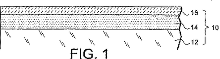
図1は、SiCOI(silicon carbide on insulant:絶縁体上のシリコンカーバイド)基板10を示している。この基板は、特に、“Smart Cut”と示される既知な切断技術を実行することにより製造することができる。図示された実施例では、この基板は、機械的な基体を構成するシリコンからなる厚い層12を含む。この層は、酸化シリコンからなる埋め込み絶縁層14、及び単結晶のシリコンカーバイドからなる表面層16により、この順で被覆される。シリコンは、他の材料で置き換えても良く、絶縁層の場合も同様である。後者としては、例えば、Si3N4が挙げられる。
FIG. 1 shows a silicon carbide on insulator (SiCOI)
特に、ここで示す実施例では、シリコンからなる層12は、厚さ100μm〜500μmであり、n型不純物がドープされている。ドーピングは、特に、基板を背面コンタクトとして用いる予定である場合、電流が流れるのに十分となるように選択される。この点については、更に後述する。
In particular, in the embodiment shown here, the
酸化シリコンの埋め込み層の機能は、本装置の異なる活性部分間の電気絶縁をとることがその1つである。その層の厚さは、逆耐電圧条件の関数として調整される。例えば、1μmの厚さで約200ボルトの電圧に耐えうるとすれば、その厚さは、1μm〜5μmとなる。 One of the functions of the buried layer of silicon oxide is to provide electrical insulation between different active parts of the device. The thickness of the layer is adjusted as a function of the reverse withstand voltage condition. For example, if a thickness of 1 μm can withstand a voltage of about 200 volts, the thickness is 1 μm to 5 μm.
単結晶SiCの表面層は、0.1μm〜3μmの厚さである。この層は、不純物濃度を1015cm−3〜5.1017cm−3のオーダーで、p型、又はn型不純物がドープされている。 The surface layer of the single crystal SiC has a thickness of 0.1 μm to 3 μm. This layer is doped with p-type or n-type impurities with an impurity concentration of the order of 10 15 cm −3 to 5.10 17 cm −3 .
図2は、オーミック接触の製造での第1の段階を示している。この段階は、シリコンカーバイド層中にドープ領域20を形成する工程を含む。ドープ領域は、シリコンカーバイド層16と同じタイプの電気伝導度を有するが、より高濃度の不純物を含む。例えば、窒素注入を用いるとn+型ドープとなり、続いて金属の堆積を伴って良好なオーミック接触を形成することができる。ドープ領域の横方向の拡張は、酸化シリコンの注入マスク22により決定され、通常のフォトリソグラフィ技術により形成されている。ドープ領域の深さ方向の拡張は、100nm〜200nmのオーダーである。それは、注入エネルギーにより決定される。
FIG. 2 shows the first stage in the production of an ohmic contact. This step includes forming a doped
そして、ドープ種の活性化を意図として注入アニールを行った後、注入マスク22を取り除く。
Then, after performing implantation annealing for the purpose of activating the doped species, the
次の段階では、図2に示すように、シリコンカーバイド層16の表面に、酸化シリコン、窒化シリコンなどの誘電体材料の絶縁体からなる層24を堆積する工程を含む。この層の堆積は、良好な誘電特性を付与するため、優先的に高温下で行う。例えば、化学気相成長法(CVD)により3μm厚の酸化シリコン層を得ることができる。
The next step includes a step of depositing a
絶縁体層24は、孔26を設け且つシリコンカーバイド層のドープ領域20の一部を露出するように、エッチングにより形付けられる。リソグラフィ剤は、孔径を正確に制御するために、優先的にCH3やSF5のフッ素化プラズマ材料である。さらに、これらは、点線及び破線により外形を示したマスクにより設定される。
図中から分かるように、孔26は、ドープ領域の下方にある範囲を有しており、しかも、このドープ領域の中央部と一致する。これにより、ドープ領域の境界部分を設けることができ、この境界部分が絶縁体層24により被覆される。境界部分は、dで示された拡張部分とともに、後述するカソード端子の金属層とドープ領域の縁部との間の距離を設定している。この手段により、カソード電界を減少させ、そのため装置の耐電圧を増加させることができる。
As can be seen from the figure, the
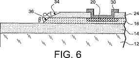
図4に、カソード端子の形成を示す。基板上には、ドープ領域20と接触しオーミック接触を形成するように、W,Ni,Tiなどの金属からなる層30を堆積する。ここで示した実施例では、厚さ50nm〜500nmのタングステンからなる層をカソードスパッタリングにより堆積する。その後、これを、図示しないマスクに従って、カソード端子の形状を決めるように、ウェット工程又はプラズマによりエッチングする。そして、材料によって900℃〜1300℃のオーダーの温度で加熱処理を2分間施し、オーミック接触をアニール処理するようにする。なお、この処理は、マスクを除去した後で行う。
FIG. 4 shows the formation of the cathode terminal. A
次に、アノード端子の形成に関して説明する。この処理の第1の段階は、図5に示すように、シリコンカーバイド層16の新たな別の一部を露出するように、絶縁体層24をエッチングする工程を含む。このエッチングの際中、絶縁層24の一部は、破線で示したマスクにより保護され維持されている。エッチングパラメータ、特に、エッチング選択性は、好ましくは、絶縁体層の主面の平面に対して20°〜80°の角度αの傾斜を有するエッチング側面34を絶縁体層24に付与するように調整される。
Next, formation of the anode terminal will be described. The first stage of this process includes the step of etching the
次いで、リソグラフィ・マスクを取り外す。 The lithography mask is then removed.
絶縁体層24のエッチングの後、シリコンカーバイドの下層にもまた、エッチング処理を施しても良い。このエッチングは、図6に示すように、絶縁体層の残留部分をリソグラフィ・マスクとして用いて行う。
After the insulating
ここで、絶縁体層24に対する選択性を制御するために、再度、エッチングパラメータを調整し、これにより、また主面に対してある角度を形成するシリコンカーバイド層16の縦方向側面36が表に出る。このβで示された角度は、好ましくは、20°〜80°であり、例えば、45°であると良い。エッチングは、絶縁体層に対する選択性を改良するために多少の酸素が混入されたSF6などのフッ素化プラズマ材料を用いて行う。多少顕著な選択性を持たせれば、より急勾配な又はより勾配の少ない傾斜を縦方向側面36に形成することができる。このとき、エッチングは、埋め込み絶縁体層14上にバリアーを覆って行う。なお、簡略化のため、角度αは、このエッチング際中で変更されないものとする。
Here, in order to control the selectivity with respect to the
このように、絶縁層24及びシリコンカーバイド層14の縦方向側面34及び36に傾斜α及びβを設けることで、シリコンカーバイド層上に金属のショットキー接合を容易に形成することができる。また、これらの傾斜は、装置のスペース要件及び電気特性に影響する。
Thus, by providing the inclinations α and β on the longitudinal side surfaces 34 and 36 of the insulating
ここで、穏やかな傾斜、言い換えれば小さい角度であれば、シリコンカーバイド層16上に形成された接合表面を増加することができ、その結果、接合の耐電圧を増加することができる。しかしながら、穏やかな傾斜は、基板表面上の構成部品のスペース要求を厳しくしてしまう。逆に、鋭角な傾斜であれば、技術的に困難であるという点を犠牲にするがスペースの節約が可能となる。
Here, if the inclination is gentle, in other words, a small angle, the bonding surface formed on the
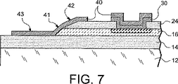
図7は、ショットキー接合の形成を示している。金属層、好ましくは、チタン又はニッケルを含む接合層40を、特に、シリコンカーバイド層16の縦方向側面36を被覆するように、基板上に堆積する。その金属層は、厚さが50nm〜300nmのオーダーであり、露出面全体に対してスパッタリング又は蒸着により堆積され、その後、図示しないマスクに従ってエッチングにより形付けられる。
FIG. 7 illustrates the formation of a Schottky junction. A
接合層は、数層の副層で形成されていても良い。特に実施例では、接合層は、Ti金属層、TiN中間層、及びAl表面層からこの順で構成することができる。これらの層については、明確なため、図中では詳細を示さないものとする。 The bonding layer may be formed of several sublayers. In particular, in the embodiment, the bonding layer can be composed of a Ti metal layer, a TiN intermediate layer, and an Al surface layer in this order. For the sake of clarity, these layers are not shown in detail in the figure.
Ti金属層は、それ自身でシリコンカーバイド層との接合を形成する。Al層の機能は、金属化の抵抗を下げ、またこれによって許容可能な直列電流密度を増やすことである。さらに、アルミニウムは、装置をハウジング内に載置する際に、アルミニウムにも外部接続線を溶接することを容易にする。上述した層は、図7に示すように、カソード端子を形成する第1の金属層30を被覆することもできる。図中では、接合層40がカソード端子のオーミック接触層30を正に被覆しているが、カソード端子周りにはみ出しても良いし、より簡単な構成には、カソード端子の層30を被覆していなくても良い。
The Ti metal layer itself forms a bond with the silicon carbide layer. The function of the Al layer is to lower the metallization resistance and thereby increase the allowable series current density. Furthermore, aluminum makes it easy to weld external connection wires to aluminum when the device is placed in the housing. The layer described above can also cover the
接合層40は、異なる機能の幾つかの部分を有する。第1の部分41は、シリコンカーバイド層16に接触している。上述したように、この部分は、ショットキー接合機能を発揮する。
The
第2の部分42は、絶縁体からなる表面層24を部分的に被覆し、特にこの層の横表面34を被覆する。この第2の部分は、フィールドプレートの機能を有する。言い換えれば、その目的は、強電界臨界領域をショットキー接合の縁から絶縁体の表面層24の厚部へと移動させることである。前述したように、シリコンカーバイド層16は、絶縁体の表面層24をリソグラフィ・マスクとして利用することによりエッチングされる。したがって、これら層の横表面は、自己整合される。
The
参照番号43で示す接合層の第3の部分は、シリコンカーバイド層16のエッチング際中に露出した埋め込み絶縁層14の一部の上に載っている。また、前述したように、この埋め込み層は、エッチングバリアーとして用いられる。第3の部分43は、構成部品を外部と接続するのに良好な相手先となる。
A third portion of the bonding layer indicated by
層16及び24の縦方向側面34及び36により形成された角α及びβがそれほど急勾配でない場合、接合層40により均一な塗膜を得ることができる。
If the angles α and β formed by the longitudinal side surfaces 34 and 36 of the
図8は、本装置のパッシベーションを含む最終段階を示している。ポリイミドなどの材料、又は他の絶縁材料のパッシベーション層50は、前述した部分を覆うように本装置に堆積される。この層は、例えば、水平旋回器により、2μm〜20μmのオーダーの厚さで堆積することができる。またこれにより、構成部品の表面を平坦にすることができる。軸52及び軸54は、アノード及びカソードにアクセスするものであり、アルミニウム線によりハウジングに接続可能となるようにこの層に設けることができる。
FIG. 8 shows the final stage including the passivation of the device. A
図8に係る装置では、アノード及びカソードの接触点は、パッシベーション層50を支持する表面の場合、同一表面上となる。便宜上、この表面を“前面”と称する。また、シリコン厚層12により形成される反対側の表面を“裏面”と称する。
In the apparatus according to FIG. 8, the contact point between the anode and the cathode is on the same surface in the case of the surface supporting the
以下、裏面にアノード接触点を有する装置の変形例について、次の図面を参照して説明する。 Hereinafter, a modified example of the apparatus having the anode contact point on the back surface will be described with reference to the following drawings.
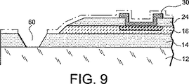
図9は、図6及び図7に示す段階の間に生じるエッチング段階を示している。この段階では、シリコンの厚層にアクセスする開口部60が埋め込み絶縁層14を通してエッチングされる。ウェット工程又はプラズマにより得られた開口部は、シリコンカーバイド層16のエッチング中に予め露出した埋め込み絶縁層14の一部に局在化する。この開口部の位置は、点線及び破線として外形を図示したマスクにより設定される。
FIG. 9 shows the etching steps that occur during the steps shown in FIGS. At this stage, an
図10は、続けて形成された金属接合層40が一部44を有し、この一部がシリコン層12とオーミック接触するように、アクセス用の開口部60に延びている様子を示している。図9及び図10から明らかなように、エッチングはまた、緩やかな傾斜の逃げ面を得るように埋め込み絶縁層14にも施される。傾斜は、例えば、30°〜70°である。これにより、金属接合層40の良好な連続性が得られる。
FIG. 10 shows a state in which the subsequently formed
図11は、構成部品を調整する最終段階を示している。パッシベーション層50が前面を覆い、カソード端子用のアクセス軸52が設けられている。
FIG. 11 shows the final stage of adjusting the components. A
構成部品の裏面には、シリコン層12を覆う金属化層60が設けられていることにも留意されたい。これは、例えば、Ti層、Ni層、そしてAu層の順番でこれらからなる3重層である。かかる構造によれば、優れた接触点を設けることができ、以後ハウジングに装置を接着するのを容易とする。なお、図8を参照して説明した開口部54は、意味がなくなる。上述の製造工程では、第1及び第2の金属層は、特に、一般的にはオーミック接触層及び接合層は、これら層上に特定の設計を施すように形付けることができる。なお、これは、特に、図4、図7及び図10に示した段階中で行うことができる。
It should also be noted that a
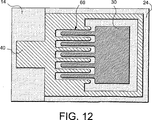
図12は、これら層の特定の構造を示している。アノード形成接合層40と第1のカソード形成金属層30は、中間領域66に亘って延設されており、この領域でこれらの層が互いにかみ合った櫛構造をなしている。かかる構造によれば、分極状態の順方向電流を増加することができる。
FIG. 12 shows the specific structure of these layers. The anode forming
以上で示した製造方法に係るダイオードの製造によれば、異なる構成部品間の絶縁を自動的に得ることができる。実例として、図13は、同一基板10上に形成された2つのダイオードの断面図を示している。第1のダイオードは、全体を図示したが、参照記号1aで識別されるものであり、第2のダイオードは、その半分だけを図示したが、参照番号1bで識別されるものである。また、2つのダイオードのアノード端子及びカソード端子を識別するために、金属層の参照番号30及び40の後に、ダイオード1a及び1bに対応する文字a及びbを付与する。なお、これら層の対象に対しては、既に記載した説明を参照すると良い。2つのダイオード間の中間領域70では、パッシベーション層50が埋め込み絶縁層14と直接接触している。これは、シリコンカーバイド層を埋め込み絶縁層上にバリアーを設けた状態でエッチングしたことにより生じる。このようにして、領域70は、構成部品間に完全な電気的絶縁をもたらす。また、接合層40a及び40b、又は金属コンタクト層30a及び30bの調整工程中は、構成部品間のあらゆる接続を得ることができる。実際、これらの層は、同一基板上に形成された構成部品の全てについて付随するように各々エッチングされる。このため、1つ以上のダイオードを直列又は並列に接続することができる。
According to the manufacturing of the diode according to the manufacturing method described above, insulation between different components can be automatically obtained. As an illustration, FIG. 13 shows a cross-sectional view of two diodes formed on the
本発明に係る装置は、ダイオードとは離れて、特に電界効果トランジスタなどの他の構成部品を備えても良い。このことは、かかるトランジスタを同一基板上に一体化する可能性を表している図14に示されている。トランジスタは、参照番号80、82、及び84のそれぞれにより識別されるゲート、ソース、及びドレインの各端子を備える。ソース82及びドレイン84の製造方法は、ダイオードのオーミック接触端子の製造方法と同じである。言い換えれば、金属コンタクト層30がシリコンカーバイド層16のドープ領域20に接触する。このため、前述の説明をまた参照することができる。まず、絶縁体の表面層24に開口部を形成し、その後、その中に金属コンタクト層30を堆積することにより、ゲートが得られる。特に、用いた工程がショットキーダイオード用として前述したものである場合、言い換えれば、MESFETトランジスタとショットキーダイオードの両方を得ることを希望する場合、開口部は、フレア側面を伴って形成することができる。しかしながら、フレア側面は、トランジスタの動作には必ずしも必要ではない。絶縁体層24に形成されたゲートの開口部は、バリアーを用いてエッチングすることによりシリコンカーバイド層上に設ける。このようなゲート80を形成するように形付けられた層部30は、シリコンカーバイド層の主面上にあるが、その縦方向側面の1つにはない。ゲートは、ショットキー接合を形成する。ここで、シリコンカーバイド層16は、トランジスタのチャネルを構成する。
The device according to the invention may comprise other components apart from the diodes, in particular field effect transistors. This is illustrated in FIG. 14, which illustrates the possibility of integrating such transistors on the same substrate. The transistor comprises gate, source, and drain terminals identified by
10 基板
12 固体キャリア
14 埋め込み層
16 シリコンカーバイド層
20 ドープ領域
24 表面層
30,40 金属層
34,36 逃げ面
10
Claims (13)
前記シリコンカーバイド層(16)の表面層との間に少なくとも1つのショットキーコンタクトを有し、アノードを構成する第1の金属層(40)と、前記シリコンカーバイド層を被覆する絶縁体の表面層とを備え、
前記第1の金属層(40)は、前記シリコンカーバイド層(16)を被覆し且つ該シリコンカーバイド層の前記側面(36)に隣接する絶縁体からなる表面層(24)の1つの側面(34)を少なくとも部分的に覆って伸長するとともに、前記シリコンカーバイド層(16)の側面(36)と接触し、
前記シリコンカーバイド層の前記側面(36)は、前記シリコンカーバイド層(16)層の主面に対して角(β:20°<β<80°)を形成するとともに、
前記絶縁体からなる表面層(24)の側面(34)は、前記絶縁体からなる表面層(24)の主面に対して角(α:20°<α<80°)を形成することを特徴とするパワージャンクションデバイス。A power junction device with SiCOI type substrate (10) having a buried layer made of an insulating material silicon carbide layer that is insulated from the solid substrate (12) by (14) (16),
A first metal layer (40) having at least one Schottky contact with the surface layer of the silicon carbide layer (16) and constituting an anode, and a surface layer of an insulator covering the silicon carbide layer And
The first metal layer (40) covers one side (34 ) of a surface layer (24) made of an insulator covering the silicon carbide layer (16) and adjacent to the side (36) of the silicon carbide layer. ) At least partially over and in contact with the side surface (36) of the silicon carbide layer (16),
The side surface (36) of the silicon carbide layer forms an angle (β: 20 ° <β <80 °) with respect to the main surface of the silicon carbide layer (16) layer ,
The side of the surface layer ing an insulator (24) (34), the angle to the main surface of the surface layer (24) made of an insulator (α: 20 ° <α < 80 °) to form a Power junction device characterized by
前記角(β)は、前記埋め込み絶縁層(14)と接触する前記シリコンカーバイド層(16)の主面に対して測定され、45°であることを特徴とするパワージャンクションデバイス。The power junction device according to claim 1,
The angle (β) is measured with respect to the main surface of the silicon carbide layer (16) in contact with the buried insulating layer (14) and is 45 °, characterized in that it is 45 °.
前記シリコンカーバイド層とオーミック接触し、カソードを形成する第2の金属層(30)を備えることを特徴とするパワージャンクションデバイス。The power junction device according to claim 1,
A power junction device comprising a second metal layer (30) in ohmic contact with the silicon carbide layer to form a cathode.
前記アノードを形成する前記第1の金属層(40)は、シリコンからなる前記固体基体まで延設されることを特徴とするパワージャンクションデバイス。The power junction device according to claim 1,
The power junction device, wherein the first metal layer (40) forming the anode extends to the solid substrate made of silicon.
少なくとも1つのパワーダイオードと少なくとも1つのトランジスタとを備え、前記トランジスタは、前記シリコンカーバイド層に形成されたチャネルを有することを特徴とするパワージャンクションデバイス。The power junction device according to claim 1,
A power junction device comprising at least one power diode and at least one transistor, the transistor having a channel formed in the silicon carbide layer.
直列又は並列に接続された複数のパワーダイオードを備えることを特徴とするパワージャンクションデバイス。The power junction device according to claim 1,
A power junction device comprising a plurality of power diodes connected in series or in parallel.
前記第1及び第2の金属層は、櫛状部をそれぞれ備え、前記第1及び第2の金属層の前記櫛状部が互いにかみ合うことを特徴とするパワージャンクションデバイス。The power junction device according to claim 4,
The first and second metal layers each include a comb-shaped portion, and the comb-shaped portions of the first and second metal layers mesh with each other.
a)前記シリコンカーバイド層の前記埋め込み絶縁層とは反対側の一表面にオーミック接触点を形成し、
b)オーミック接触点の形成に先立ち、前記シリコンカーバイド層上に絶縁体からなる表面層(24)を形成するとともに、前記シリコンカーバイド層の前記側面(36)は、前記シリコンカーバイド層の主面に対して角(β:20°<β<80°)を形成し、かつ
前記絶縁体からなる表面層(24)の側面(34)が、前記シリコンカーバイド層の前記側面(36)に隣接し、前記絶縁体からなる表面層(24)の主面に対して角(α:20°<α<80°)を形成するように、
前記オーミック接触の領域の外側で、前記絶縁体からなる表面層(24)およびシリコンカーバイド層を局所的にエッチングし、
c)次いで、前記絶縁体からなる表面層の側面および前記シリコンカーバイド層の側面を被覆する金属層(40)を堆積することにより、前記縦方向側面上にショットキー接触部を形成する、
ステップを含むことを特徴とするパワージャンクションデバイスの製造方法。A power junction device manufacturing method for manufacturing a power junction device on a SiCOI substrate having a silicon carbide layer (16) insulated from a solid substrate (12) made of silicon by a buried layer (14) of an insulator,
a) forming an ohmic contact point on one surface of the silicon carbide layer opposite to the buried insulating layer;
Prior to formation of b) ohmic contact points, thereby forming a surface layer (24) made of an insulating material on the silicon carbide layer, the side surface of the silicon carbide layer (36), the main surface of the silicon carbide layer Forming an angle (β: 20 ° <β <80 °), and
The side surface (34) of the surface layer (24) made of the insulator is adjacent to the side surface (36) of the silicon carbide layer, and has an angle (α) with respect to the main surface of the surface layer (24) made of the insulator. : 20 ° <α <80 °)
The outside of the ohmic contact region, locally etching the surface layer (24) and the silicon carbide layer consisting of the insulating body,
c) Then, by depositing a metal layer covering (40) the side surfaces and side surfaces of the silicon carbide layer on the surface layer made of the insulator, forming a Schottky contact portion on said longitudinal sides,
A method for manufacturing a power junction device, comprising: steps.
前記局所的なエッチングは、前記縦方向側面に傾斜を付与するように、リソグラフィ・マスクと、前記リソグラフィ・マスクに対する特定の選択性を有するリソグラフィ剤とを用いてエッチングするようにしたことを特徴とするパワージャンクションデバイスの製造方法。It is a manufacturing method of the power junction device according to claim 8,
The local etching is performed using a lithography mask and a lithographic agent having a specific selectivity with respect to the lithography mask so as to impart inclination to the longitudinal side surface. A method of manufacturing a power junction device.
前記絶縁層の表面層(24)は、前記ステップb)でリソグラフィ・マスクとして用いられることを特徴とするパワージャンクションデバイスの製造方法。A method of manufacturing a power junction device according to claim 9,
The method of manufacturing a power junction device, wherein the surface layer (24) of the insulating layer is used as a lithography mask in the step b).
前記ショットキー接触部は、金属層(40)と前記シリコンカーバイド層(16)との間に形成され、前記金属層(40)は、前記絶縁体からなる表面層(24)を部分的に覆って延設されていることを特徴とするパワージャンクションデバイスの製造方法。A method of manufacturing a power junction device according to claim 9,
The Schottky contact portion is formed between the metal layer (40) and said silicon carbide layer (16), said metal layer (40), the surface layer (24) partially covering consisting of the insulator A method of manufacturing a power junction device, wherein the power junction device is extended.
前記ショットキー接触部は、金属層(40)と前記シリコンカーバイド層(16)との間に形成され、前記金属層(40)は、前記埋め込み絶縁層(14)に予め設けた開口部を通して前記固体基体(12)まで延設されていることを特徴とするパワージャンクションデバイスの製造方法。It is a manufacturing method of the power junction device according to claim 7,
The Schottky contact portion is formed between a metal layer (40) and the silicon carbide layer (16), and the metal layer (40) passes through an opening provided in advance in the buried insulating layer (14). A method of manufacturing a power junction device, wherein the power junction device extends to a solid substrate (12).
オーミック接触点を形成する前記ステップは、前記シリコンカーバイド層にドープ領域(20)を形成し、その後、金属層(30)と前記ドープ領域(20)の周辺との間に重なり部分(d)を設けることにより、前記金属層(30)を前記ドープ領域の中央部に接触させて堆積することを特徴とするパワージャンクションデバイスの製造方法。It is a manufacturing method of the power junction device according to claim 7,
The step of forming an ohmic contact includes forming a doped region (20) in the silicon carbide layer, and then forming an overlapping portion (d) between the metal layer (30) and the periphery of the doped region (20). A method for manufacturing a power junction device, comprising: depositing the metal layer (30) in contact with a central portion of the doped region.
Applications Claiming Priority (2)
| Application Number | Priority Date | Filing Date | Title |
|---|---|---|---|
| FR0203165A FR2837322B1 (en) | 2002-03-14 | 2002-03-14 | SiCOI SUBSTRATE POWER SCHOTTKY DIODE AND METHOD FOR MAKING SAME |
| PCT/FR2003/000787 WO2003077321A2 (en) | 2002-03-14 | 2003-03-12 | Schottky power diode comprising a sicoi substrate and the method of producing one such diode |
Publications (2)
| Publication Number | Publication Date |
|---|---|
| JP2005531127A JP2005531127A (en) | 2005-10-13 |
| JP4593115B2 true JP4593115B2 (en) | 2010-12-08 |
Family
ID=27772110
Family Applications (1)
| Application Number | Title | Priority Date | Filing Date |
|---|---|---|---|
| JP2003575425A Expired - Lifetime JP4593115B2 (en) | 2002-03-14 | 2003-03-12 | Schottky power diode provided with SiCOI substrate and method of manufacturing the same |
Country Status (7)
| Country | Link |
|---|---|
| US (1) | US7166894B2 (en) |
| EP (1) | EP1483793B1 (en) |
| JP (1) | JP4593115B2 (en) |
| AT (1) | ATE522932T1 (en) |
| AU (1) | AU2003233372A1 (en) |
| FR (1) | FR2837322B1 (en) |
| WO (1) | WO2003077321A2 (en) |
Families Citing this family (13)
| Publication number | Priority date | Publication date | Assignee | Title |
|---|---|---|---|---|
| US9515135B2 (en) * | 2003-01-15 | 2016-12-06 | Cree, Inc. | Edge termination structures for silicon carbide devices |
| US7026650B2 (en) * | 2003-01-15 | 2006-04-11 | Cree, Inc. | Multiple floating guard ring edge termination for silicon carbide devices |
| WO2006041144A1 (en) * | 2004-10-13 | 2006-04-20 | Semiconductor Energy Laboratory Co., Ltd. | Etching method and manufacturing method of semiconductor device |
| US20090223292A1 (en) * | 2006-09-28 | 2009-09-10 | Hitachi Metals, Ltd. | Acceleration sensor |
| JP2008190961A (en) * | 2007-02-02 | 2008-08-21 | Hitachi Metals Ltd | Piezo-resistive acceleration sensor |
| WO2008148095A1 (en) * | 2007-05-25 | 2008-12-04 | Astralux, Inc. | Hybrid silicon/non-silicon electronic device with heat spreader |
| JP2009076866A (en) * | 2007-08-31 | 2009-04-09 | Sumitomo Electric Ind Ltd | Schottky barrier diode |
| US8518811B2 (en) * | 2011-04-08 | 2013-08-27 | Infineon Technologies Ag | Schottky diodes having metal gate electrodes and methods of formation thereof |
| KR102099438B1 (en) * | 2013-10-07 | 2020-04-09 | 엘지이노텍 주식회사 | Semiconductor device |
| US10971580B2 (en) * | 2016-12-15 | 2021-04-06 | Griffith University | Silicon carbide schottky diodes with tapered negative charge density |
| GB2569196B (en) * | 2017-12-11 | 2022-04-20 | Pragmatic Printing Ltd | Schottky diode |
| US10615292B2 (en) * | 2018-03-27 | 2020-04-07 | Hong Kong Applied Science And Technology Research Institute Co., Ltd. | High voltage silicon carbide Schottky diode flip chip array |
| JP6968042B2 (en) * | 2018-07-17 | 2021-11-17 | 三菱電機株式会社 | SiC-SOI device and its manufacturing method |
Family Cites Families (25)
| Publication number | Priority date | Publication date | Assignee | Title |
|---|---|---|---|---|
| FR1111688A (en) | 1954-09-22 | 1956-03-02 | Flower vase | |
| US4045248A (en) * | 1973-06-26 | 1977-08-30 | U.S. Philips Corporation | Making Schottky barrier devices |
| JPS519383A (en) * | 1974-07-11 | 1976-01-26 | Sony Corp | HANDOTA ISOCHI |
| JPS5640677U (en) * | 1979-09-07 | 1981-04-15 | ||
| DE3219606A1 (en) * | 1982-05-25 | 1983-12-01 | Siemens AG, 1000 Berlin und 8000 München | SCHOTTKY PERFORMANCE DIODE |
| JPS6173345A (en) * | 1984-09-19 | 1986-04-15 | Toshiba Corp | Semiconductor device |
| JPS6423569A (en) * | 1987-07-20 | 1989-01-26 | Matsushita Electronics Corp | Schottky barrier semiconductor |
| JPH067594B2 (en) * | 1987-11-20 | 1994-01-26 | 富士通株式会社 | Method for manufacturing semiconductor substrate |
| US6573534B1 (en) * | 1995-09-06 | 2003-06-03 | Denso Corporation | Silicon carbide semiconductor device |
| AU1531797A (en) * | 1996-01-24 | 1997-08-20 | Cree Research, Inc. | Mesa schottky diode with guard ring |
| US5898210A (en) * | 1996-06-14 | 1999-04-27 | The United States Of America As Represented By The Secretary Of The Army | Semiconductor diode with high turn on and breakdown voltages |
| US5880491A (en) * | 1997-01-31 | 1999-03-09 | The United States Of America As Represented By The Secretary Of The Air Force | SiC/111-V-nitride heterostructures on SiC/SiO2 /Si for optoelectronic devices |
| US6784489B1 (en) * | 1997-03-28 | 2004-08-31 | Stmicroelectronics, Inc. | Method of operating a vertical DMOS transistor with schottky diode body structure |
| DE19723176C1 (en) | 1997-06-03 | 1998-08-27 | Daimler Benz Ag | Semiconductor device with alternate p-n and Schottky junctions |
| JPH1174498A (en) * | 1997-08-29 | 1999-03-16 | N T T Electron Kk | Semiconductor integrated device |
| FR2774214B1 (en) * | 1998-01-28 | 2002-02-08 | Commissariat Energie Atomique | PROCESS FOR PRODUCING A SEMICONDUCTOR TYPE STRUCTURE ON INSULATOR AND IN PARTICULAR SiCOI |
| DE19954866A1 (en) | 1999-11-15 | 2001-05-31 | Infineon Technologies Ag | Process for treating a surface of an SiC semiconductor body produced by epitaxy and Schottky contact produced thereafter |
| US6903373B1 (en) * | 1999-11-23 | 2005-06-07 | Agere Systems Inc. | SiC MOSFET for use as a power switch and a method of manufacturing the same |
| FR2803103B1 (en) | 1999-12-24 | 2003-08-29 | St Microelectronics Sa | SCHOTTKY DIODE ON SILICON CARBIDE SUBSTRATE |
| US6566680B1 (en) * | 2001-01-30 | 2003-05-20 | Advanced Micro Devices, Inc. | Semiconductor-on-insulator (SOI) tunneling junction transistor |
| US6509613B1 (en) * | 2001-05-04 | 2003-01-21 | Advanced Micro Devices, Inc. | Self-aligned floating body control for SOI device through leakage enhanced buried oxide |
| US6566158B2 (en) * | 2001-08-17 | 2003-05-20 | Rosemount Aerospace Inc. | Method of preparing a semiconductor using ion implantation in a SiC layer |
| US6689669B2 (en) * | 2001-11-03 | 2004-02-10 | Kulite Semiconductor Products, Inc. | High temperature sensors utilizing doping controlled, dielectrically isolated beta silicon carbide (SiC) sensing elements on a specifically selected high temperature force collecting membrane |
| US6656811B2 (en) * | 2001-12-21 | 2003-12-02 | Texas Instruments Incorporated | Carbide emitter mask etch stop |
| US6764907B2 (en) * | 2002-02-19 | 2004-07-20 | Bart J. Van Zeghbroeck | Method of fabricating self-aligned silicon carbide semiconductor devices |
-
2002
- 2002-03-14 FR FR0203165A patent/FR2837322B1/en not_active Expired - Fee Related
-
2003
- 2003-03-12 AU AU2003233372A patent/AU2003233372A1/en not_active Abandoned
- 2003-03-12 EP EP03727583A patent/EP1483793B1/en not_active Expired - Lifetime
- 2003-03-12 WO PCT/FR2003/000787 patent/WO2003077321A2/en active Application Filing
- 2003-03-12 AT AT03727583T patent/ATE522932T1/en not_active IP Right Cessation
- 2003-03-12 US US10/507,757 patent/US7166894B2/en not_active Expired - Lifetime
- 2003-03-12 JP JP2003575425A patent/JP4593115B2/en not_active Expired - Lifetime
Also Published As
| Publication number | Publication date |
|---|---|
| ATE522932T1 (en) | 2011-09-15 |
| FR2837322B1 (en) | 2005-02-04 |
| US7166894B2 (en) | 2007-01-23 |
| AU2003233372A8 (en) | 2003-09-22 |
| WO2003077321A3 (en) | 2004-04-15 |
| EP1483793B1 (en) | 2011-08-31 |
| JP2005531127A (en) | 2005-10-13 |
| FR2837322A1 (en) | 2003-09-19 |
| WO2003077321A2 (en) | 2003-09-18 |
| US20050161760A1 (en) | 2005-07-28 |
| AU2003233372A1 (en) | 2003-09-22 |
| EP1483793A2 (en) | 2004-12-08 |
Similar Documents
| Publication | Publication Date | Title |
|---|---|---|
| JP3559971B2 (en) | Silicon carbide semiconductor device and method of manufacturing the same | |
| JP5525940B2 (en) | Semiconductor device and manufacturing method of semiconductor device | |
| JP6241572B2 (en) | Semiconductor device | |
| US9029986B2 (en) | Transistors with dual layer passivation | |
| US3617824A (en) | Mos device with a metal-silicide gate | |
| US8138581B2 (en) | Semiconductor device with channel stop trench and method | |
| JP4593115B2 (en) | Schottky power diode provided with SiCOI substrate and method of manufacturing the same | |
| US20170141190A1 (en) | Gan-on-si switch devices | |
| CN111656498B (en) | Semiconductor device and method for manufacturing the same | |
| JP5889171B2 (en) | Silicon carbide semiconductor device and manufacturing method thereof | |
| US20220059659A1 (en) | Semiconductor Device with Silicon Carbide Body and Method of Manufacturing | |
| CN111029404A (en) | P-GaN/AlGaN/GaN enhancement device based on fin-shaped gate structure and manufacturing method thereof | |
| CN111863807A (en) | Single-chip heterogeneous integrated Cascode structure field effect transistor based on source field plate and manufacturing method | |
| JP2008210938A (en) | Semiconductor device and manufacturing method thereof | |
| US9490355B2 (en) | Silicon carbide static induction transistor and process for making a silicon carbide static induction transistor | |
| JP2020202345A (en) | Semiconductor device and manufacturing method thereof | |
| JPH0573067B2 (en) | ||
| JP2023079185A (en) | SiC-BASED ELECTRONIC DEVICE WITH ENHANCED ROBUSTNESS, AND METHOD FOR MANUFACTURING ELECTRONIC DEVICE | |
| JP2000323665A (en) | Manufacture of semiconductor device | |
| JP4876418B2 (en) | Semiconductor device | |
| JP5991629B2 (en) | Semiconductor device and manufacturing method of semiconductor device | |
| JPH10117002A (en) | Schottky barrier semiconductor device and its manufacturing method | |
| US8866264B2 (en) | Semiconductor device and manufacturing method of the same | |
| JPH08236791A (en) | Schottky barrier semiconductor device | |
| JP2013008783A (en) | Method of manufacturing semiconductor device, and semiconductor device |
Legal Events
| Date | Code | Title | Description |
|---|---|---|---|
| A521 | Request for written amendment filed |
Free format text: JAPANESE INTERMEDIATE CODE: A523 Effective date: 20050714 |
|
| A621 | Written request for application examination |
Free format text: JAPANESE INTERMEDIATE CODE: A621 Effective date: 20060217 |
|
| RD04 | Notification of resignation of power of attorney |
Free format text: JAPANESE INTERMEDIATE CODE: A7424 Effective date: 20060424 |
|
| A977 | Report on retrieval |
Free format text: JAPANESE INTERMEDIATE CODE: A971007 Effective date: 20090205 |
|
| A131 | Notification of reasons for refusal |
Free format text: JAPANESE INTERMEDIATE CODE: A131 Effective date: 20090526 |
|
| A601 | Written request for extension of time |
Free format text: JAPANESE INTERMEDIATE CODE: A601 Effective date: 20090826 |
|
| A602 | Written permission of extension of time |
Free format text: JAPANESE INTERMEDIATE CODE: A602 Effective date: 20090902 |
|
| A601 | Written request for extension of time |
Free format text: JAPANESE INTERMEDIATE CODE: A601 Effective date: 20090928 |
|
| A602 | Written permission of extension of time |
Free format text: JAPANESE INTERMEDIATE CODE: A602 Effective date: 20091005 |
|
| A601 | Written request for extension of time |
Free format text: JAPANESE INTERMEDIATE CODE: A601 Effective date: 20091026 |
|
| A602 | Written permission of extension of time |
Free format text: JAPANESE INTERMEDIATE CODE: A602 Effective date: 20091102 |
|
| A521 | Request for written amendment filed |
Free format text: JAPANESE INTERMEDIATE CODE: A523 Effective date: 20091126 |
|
| A02 | Decision of refusal |
Free format text: JAPANESE INTERMEDIATE CODE: A02 Effective date: 20100202 |
|
| A521 | Request for written amendment filed |
Free format text: JAPANESE INTERMEDIATE CODE: A523 Effective date: 20100531 |
|
| A911 | Transfer to examiner for re-examination before appeal (zenchi) |
Free format text: JAPANESE INTERMEDIATE CODE: A911 Effective date: 20100802 |
|
| TRDD | Decision of grant or rejection written | ||
| A01 | Written decision to grant a patent or to grant a registration (utility model) |
Free format text: JAPANESE INTERMEDIATE CODE: A01 Effective date: 20100817 |
|
| A01 | Written decision to grant a patent or to grant a registration (utility model) |
Free format text: JAPANESE INTERMEDIATE CODE: A01 |
|
| A61 | First payment of annual fees (during grant procedure) |
Free format text: JAPANESE INTERMEDIATE CODE: A61 Effective date: 20100915 |
|
| FPAY | Renewal fee payment (event date is renewal date of database) |
Free format text: PAYMENT UNTIL: 20130924 Year of fee payment: 3 |
|
| R150 | Certificate of patent or registration of utility model |
Ref document number: 4593115 Country of ref document: JP Free format text: JAPANESE INTERMEDIATE CODE: R150 Free format text: JAPANESE INTERMEDIATE CODE: R150 |
|
| R250 | Receipt of annual fees |
Free format text: JAPANESE INTERMEDIATE CODE: R250 |
|
| R250 | Receipt of annual fees |
Free format text: JAPANESE INTERMEDIATE CODE: R250 |
|
| R250 | Receipt of annual fees |
Free format text: JAPANESE INTERMEDIATE CODE: R250 |
|
| R250 | Receipt of annual fees |
Free format text: JAPANESE INTERMEDIATE CODE: R250 |
|
| R250 | Receipt of annual fees |
Free format text: JAPANESE INTERMEDIATE CODE: R250 |
|
| R250 | Receipt of annual fees |
Free format text: JAPANESE INTERMEDIATE CODE: R250 |
|
| R250 | Receipt of annual fees |
Free format text: JAPANESE INTERMEDIATE CODE: R250 |
|
| R250 | Receipt of annual fees |
Free format text: JAPANESE INTERMEDIATE CODE: R250 |
|
| R250 | Receipt of annual fees |
Free format text: JAPANESE INTERMEDIATE CODE: R250 |
|
| R250 | Receipt of annual fees |
Free format text: JAPANESE INTERMEDIATE CODE: R250 |
|
| EXPY | Cancellation because of completion of term |