JP4589539B2 - Semiconductor laser device and manufacturing method thereof - Google Patents
Semiconductor laser device and manufacturing method thereof Download PDFInfo
- Publication number
- JP4589539B2 JP4589539B2 JP2001013059A JP2001013059A JP4589539B2 JP 4589539 B2 JP4589539 B2 JP 4589539B2 JP 2001013059 A JP2001013059 A JP 2001013059A JP 2001013059 A JP2001013059 A JP 2001013059A JP 4589539 B2 JP4589539 B2 JP 4589539B2
- Authority
- JP
- Japan
- Prior art keywords
- semiconductor
- multilayer structure
- active layer
- semiconductor multilayer
- laser
- Prior art date
- Legal status (The legal status is an assumption and is not a legal conclusion. Google has not performed a legal analysis and makes no representation as to the accuracy of the status listed.)
- Expired - Fee Related
Links
Images


Landscapes
- Semiconductor Lasers (AREA)
Description
【0001】
【発明の属する技術分野】
本発明は、波長が異なる複数のレーザ光を出射することができる半導体レーザ装置及びその製造方法に関する。
【0002】
【従来の技術】
近年、多くの産業分野において半導体レーザ装置の需要が高まっており、III −V族化合物半導体層、特にGaAs又はInPを含む化合物半導体層を有する半導体レーザ装置を中心として、活発な研究及び開発が進められている。
【0003】
光情報処理分野においては、AlGaAs層を有し、780nm帯の波長を持つ赤外レーザ光を発振する半導体レーザ装置により情報の記録又は再生を行なう方式が実用化されており、このような半導体レーザ装置はコンパクトディスク(CD)等の分野で広く普及するに至っている。
【0004】
また、光磁気ディスク等のようにCDよりも容量の大きい記録装置では、AlGaInP層を有し、780nm帯よりも波長が短い680nm帯のレーザ光を発振する半導体レーザ装置が用いられている。
【0005】
さらに、高精細な画像を長時間再生が可能なディジタルビデオディスク(DVD)を実現するためには、650nm帯の波長を持つ赤色レーザ光を出射する半導体レーザ装置が必要になってきた。このような発振波長の短波長化によって光ディスクの記録密度の向上が図られている。
【0006】
ところで、DVD情報を再生するためのDVD装置は、DVD情報のみならず、従来のCD情報をも活用できるように、DVD及びCDの両方のディスクを再生できる互換性を持っている。従って、DVD装置のピックアップヘッド部の光源には、AlGaAs層を有し780nm帯の赤外レーザ光を出射する第1の半導体レーザ素子と、AlGaInP層を有し650nm帯の赤色レーザ光を出射する第2の半導体レーザ素子とからなる2つの半導体レーザ素子を搭載する必要がある。
【0007】
この場合、各半導体レーザ素子ごとに光学処理部を設けると、780nm帯のレーザ光と650nm帯のレーザ光とを合波させる光学系が必要になるので、ピックアップヘッド装置の構造が複雑になると共にピックアップヘッド装置の小型化に限界があるという問題がある。
【0008】
そこで、2個の半導体レーザ素子を互いに接近させて配置するハイブリッド型の半導体レーザ装置、又は1つの基板上に2つの半導体積層構造が並列に設けられてなるモノリシック型の半導体レーザ装置(特開平11−186651号公報及び第60回秋季応用物理学会学術講演会予稿集3a−ZC−10を参照)が提案されている。
【0009】
図21は、モノリシック型の従来の半導体レーザ装置の一例を示しており、該半導体レーザ装置は、1つの半導体基板1の上に、AlGaInP層を有する第1の半導体積層構造2とAlGaAs層を有する第2の半導体積層構造3とが設けられ、第1の半導体積層構造2の発光スポット4から650nm帯のレーザ光を出射すると共に第2の半導体積層構造3の発光スポット5から780nm帯のレーザ光を出射する。
【0010】
前述のハイブリッド型又はモノリシック型の半導体レーザ装置を用いると、波長帯が異なる2つのレーザ光を合波させる光学系が不要になるので、ピックアップヘッド装置の簡素化及び小型化を図ることができる。
【0011】
【発明が解決しようとする課題】
しかしながら、ハイブリッド型の半導体レーザ装置においては、2つの半導体レーザ素子のピッチは、各半導体レーザ素子の幅寸法の影響を受けるため、発光スポットのピッチは数百μm以上となる。
【0012】
また、モノリシック型の半導体レーザ装置においては、1つの半導体基板上に2つの半導体積層構造を形成する必要があり、2つの半導体積層構造を分離するプロセスの限界により、発光スポットのピッチは数十nm以上となる。
【0013】
ところで、光ピックアップヘッド装置には、レーザ光の出射方向を光ディスクの方に変えるハーフミラー、及びハーフミラーを通過したレーザ光を光ディスクのスポットに集光する対物レンズ、光ディスクから反射してきたレーザ光を検出するフォトディテクタ等が必要になる。
【0014】
ところが、光ピックアップヘッド装置の小型化に伴って、対物レンズも小型化されているため、対物レンズにおけるレーザ光の入射点の差異(発光スポットが異なるために対物レンズにおける入射点の位置が異なる)に起因して対物レンズの集光特性が異なる。このため、対物レンズを通過したレーザ光を光ディスクの微少なスポットに集光することが困難になるという問題がある。
【0015】
また、対物レンズを通過したレーザ光が光ディスクに入射する角度が互いに異なると、光ディスクから反射されてくるレーザ光の方向も異なるため、フォトディテクタが2つ必要になるという問題もある。
【0016】
前記に鑑み、本発明は、波長が異なる複数のレーザ光を、1つの発光スポット又は極めて接近した2つの発光スポットから出射させるようにすることにより、波長が異なる複数のレーザ光を光ディスクの微少なスポットに確実に集光できるようにすると共に、波長が異なる複数のレーザ光を1つのフォトディテクタで検出できるようにすることを目的とする。
【0017】
【課題を解決するための手段】
前記の目的を達成するため、本発明に係る半導体レーザ装置は、基板上の前方側の領域に設けられ、第1の波長帯を持つ第1のレーザ光を発振させる第1の活性層を有する第1の半導体積層構造と、基板上の後方側の領域に設けられ、第2の波長帯を持つ第2のレーザ光を発振させる第2の活性層を有する第2の半導体積層構造とを備え、第1のレーザ光の出射方向と第2のレーザ光の出射方向とは同方向である。
【0018】
本発明に係る半導体レーザ装置によると、基板上の前方側の領域に第1のレーザ光を発振させる第1の半導体積層構造が設けられ且つ基板上の後方側の領域に第2のレーザ光を発振させる第2の半導体積層構造が設けられていると共に、第1のレーザ光の出射方向と第2のレーザ光の出射方向とは同方向であるから、波長が異なる第1及び第2のレーザ光を、前方側の領域に設けられている第1の半導体積層構造の前端面における、1つの発光スポット又は極めて接近した2つの発光スポットから出射させることができる。このため、波長が異なる複数のレーザ光を、光ディスクの微少なスポットに確実に集光できると共に1つのフォトディテクタにより検出することができる。
【0019】
本発明に係る半導体レーザ装置において、第1のレーザ光の出射方向と第2のレーザ光の出射方向とは同一直線上にあることが好ましい。
【0020】
このようにすると、波長が異なる第1及び第2のレーザ光を、第1の半導体積層構造の前端面における1つの発光スポットから出射させることができる。
【0021】
本発明に係る半導体レーザ装置において、第2のレーザ光の出射方向は、第1のレーザ光の出射方向の上側又は下側に位置していることが好ましい。
【0022】
このようにすると、波長が異なる第1及び第2のレーザ光を、第1の半導体積層構造の前端面における極めて接近した2つの発光スポットから出射させることができる。すなわち、第1のレーザ光の発光スポットと第2のレーザ光の発光スポットとのピッチは、半導体集積構造体の幅寸法の影響を受けなくなるので、発光スポットのピッチを1μm以下にすることができる。
【0023】
また、第1の活性層の後端面を透過面又は吸収面とすることができるので、光学的な設計条件の選択肢が増える。すなわち、第1の活性層のエネルギーギャップが第2の活性層のエネルギーギャップよりも大きく且つ第1のレーザ光の光軸と第2のレーザ光の光軸とが一致している場合には、第2の活性層の前端面つまり第1の活性層の後端面は第1のレーザ光の吸収面になってしまう。通常、第2の活性層の上方又は下方の半導体層のエネルギーギャップは第2の活性層のエネルギーギャップよりも大きいため、第2のレーザ光の光軸が第1のレーザ光の光軸の上側又は下側に位置すると、第2の活性層の上方又は下方の半導体層の前端面つまり第1の活性層の後端面を第1のレーザ光の透過面又は吸収面にすることができる。
【0024】
第2のレーザ光の出射方向が第1のレーザ光の出射方向の上側又は下側に位置している場合、第2の半導体積層構造における、第1の活性層の後端面と対向する半導体層のエネルギーギャップは、第1の活性層のエネルギーギャップよりも大きいことが好ましい。
【0025】
このようにすると、第2の半導体積層構造における、第1の活性層の後端面と対向する半導体層は第1のレーザ光を透過させるため、第1のレーザ光の損失が低減する。
【0026】
また、第2のレーザ光の出射方向が第1のレーザ光の出射方向の上側又は下側に位置している場合、第1の半導体積層構造は、基板と第1の活性層との間に位置する第1のクラッド層と、第1の活性層の上方に位置する第2のクラッド層とを有し、第2の半導体積層構造は、基板と第2の活性層との間に位置する第3のクラッド層と、第2の活性層の上方に位置する第4のクラッド層とを有し、第1のクラッド層の組成と第3のクラッド層の組成とが同じであるか、又は第2のクラッド層の組成と第4のクラッド層の組成とが同じであることが好ましい。
【0027】
本発明に係る半導体レーザ装置において、第1の活性層のエネルギーギャップは、第2の活性層のエネルギーギャップよりも大きいことが好ましい。
【0028】
このようにすると、第2のレーザ光は、第1の半導体積層構造の内部を伝播する際に吸収されないので、第1の半導体積層構造の前端面から確実に出射する。
【0029】
特に、第1のレーザ光の光軸と第2のレーザ光の光軸とが一致している場合には、第2の活性層は第1の活性層で発振した第1のレーザに対する吸収係数が大きいため、第1のレーザ光は第1の半導体積層構造の前端面と第2の半導体積層構造の前端面とを共振器として発振し、また、第2の活性層で発振した第2のレーザ光は、第1の活性層に対して透明であるから、第1の半導体積層構造の前端面と第2の半導体積層構造の後端面とを共振器として発振する。従って、波長帯が異なる2つのレーザ光を1つの発光スポットから確実に出射させることができる。
【0030】
本発明に係る半導体レーザ装置において、第1の活性層はインジウム及びリンを含み、第2の活性層はガリウム及びヒ素を含むことが好ましい。
【0031】
このようにすると、第1のレーザ光の発振波長は650nm程度になるので第1のレーザ光は赤色レーザ光になると共に、第2のレーザ光の発振波長は780nm程度になるので第2のレーザ光は赤外レーザ光になるので、DVD装置のピックアップヘッド装置に最適な半導体レーザ装置が得られる。
【0032】
本発明に係る半導体レーザ装置において、第1の半導体積層構造の前端面には無反射コーティング層が設けられ、第2の半導体積層構造の後端面には高反射コーティング層が設けられていることが好ましい。
【0033】
このようにすると、波長帯が異なる2つのレーザ光を第1の半導体積層構造の前端面から確実に出射させることができる。
【0034】
本発明に係る半導体レーザ装置は、第1の半導体積層構造の後端面と第2の半導体積層構造の前端面との間に誘電体部材をさらに備え、誘電体部材は、第1の活性層のストライプ領域の実効屈折率と、第2の活性層のストライプ領域の実効屈折率との間の屈折率を持つことが好ましい。
【0035】
このようにすると、誘電体部材によって、第1の半導体積層構造と第2の半導体積層構造との絶縁性が確実となる。また、第1のレーザ光と第2の半導体積層構造との光の結合効率が向上すると共に第2のレーザ光と第1の半導体積層構造との光の結合効率が向上するため、半導体レーザ装置の光学的特性が向上する。
【0036】
本発明に係る第1の半導体レーザ装置の製造方法は、基板上の前方側の領域に設けられ、第1の波長帯を持つ第1のレーザ光を発振させる第1の活性層を有する第1の半導体積層構造と、基板上の後方側の領域に設けられ、第2の波長帯を持つ第2のレーザ光を発振させる第2の活性層を有する第2の半導体積層構造とを備えた半導体レーザ装置の製造方法を対象とし、基板上に全面に亘って、第2の半導体積層構造と同じ積層構造を有する第1の暫定半導体積層構造を成長させる工程と、第1の暫定半導体積層構造の前方側の部分を除去することにより、基板上の後方側の領域に第2の半導体積層構造を形成する工程と、基板上の前方側の領域及び第2の半導体積層構造の上に全面に亘って、第1の半導体積層構造と同じ積層構造を有する第2の暫定半導体積層構造を成長させる工程と、第2の暫定半導体積層構造における第2の半導体積層構造よりも上側の部分を除去することにより、基板上の前方側の領域に第1の半導体積層構造を形成する工程とを備えている。
【0037】
本発明に係る第1の半導体レーザ装置の製造方法によると、基板上の前方側の領域に第1のレーザ光を発振させる第1の半導体積層構造が設けられ且つ基板上の後方側の領域に第2のレーザ光を発振させる第2の半導体積層構造が設けられていると共に、第1のレーザ光の出射方向と第2のレーザ光の出射方向とが同方向であるモノリシック型の半導体レーザ装置を確実に製造することができる。
【0038】
本発明に係る第2の半導体レーザ装置の製造方法は、基板上の前方側の領域に設けられ、第1の波長帯を持つ第1のレーザ光を発振させる第1の活性層を有する第1の半導体積層構造と、基板上の後方側の領域に設けられ、第2の波長帯を持つ第2のレーザ光を発振させる第2の活性層を有する第2の半導体積層構造とを備えた半導体レーザ装置の製造方法を対象とし、基板上に全面に亘って、第1の半導体積層構造と同じ積層構造を有する第1の暫定半導体積層構造を成長させる工程と、第1の暫定半導体積層構造の後方側の部分を除去することにより、基板上の前方側の領域に第1の半導体積層構造を形成する工程と、基板上の後方側の領域及び第1の半導体積層構造の上に全面に亘って、第2の半導体積層構造と同じ積層構造を有する第2の暫定半導体積層構造を成長させる工程と、第2の暫定半導体積層構造における第1の半導体積層構造よりも上側の部分を除去することにより、基板上の後方側の領域に第2の半導体積層構造を形成する工程とを備えている。
【0039】
本発明に係る第2の半導体レーザ装置の製造方法によると、基板上の前方側の領域に第1のレーザ光を発振させる第1の半導体積層構造が設けられ且つ基板上の後方側の領域に第2のレーザ光を発振させる第2の半導体積層構造が設けられていると共に、第1のレーザ光の出射方向と第2のレーザ光の出射方向とが同方向であるモノリシック型の半導体レーザ装置を確実に製造することができる。
【0040】
本発明に係る第3の半導体レーザ装置の製造方法は、第1の波長帯を持つ第1のレーザ光を発振させる第1の活性層を有する第1のレーザチップと、第2の波長帯を持つ第2のレーザ光を発振させる第2の活性層を有する第2のレーザチップとをそれぞれ形成する第1の工程と、基板上の前方側の領域に第1のレーザチップを固定すると共に、基板上の後方側の領域に第2のレーザチップを固定する第2の工程とを備え、第2の工程は、第1のレーザ光の出射方向と第2のレーザ光の出射方向とが同方向になるように、第1のレーザチップ及び第2のレーザチップを固定する工程を含む。
【0041】
本発明に係る第3の半導体レーザ装置の製造方法によると、基板上の前方側の領域に第1のレーザ光を発振させる第1のレーザチップが設けられ且つ基板上の後方側の領域に第2のレーザ光を発振させる第2のレーザチップが設けられていると共に、第1のレーザ光の出射方向と第2のレーザ光の出射方向とが同方向であるハイブリッド型の半導体レーザ装置を確実に製造することができる。
【0042】
第1〜第3の半導体レーザ装置の製造方法において、第1のレーザ光の出射方向と第2のレーザ光の出射方向とは同一直線上にあることが好ましい。
【0043】
このようにすると、波長が異なる第1及び第2のレーザ光を、第1の半導体積層構造又は第1のレーザチップの前端面における1つの発光スポットから出射させることができる。
【0044】
第1〜第3の半導体レーザ装置の製造方法において、第2のレーザ光の出射方向は、第1のレーザ光の出射方向の上側又は下側に位置していることが好ましい。
【0045】
このようにすると、波長が異なる第1及び第2のレーザ光を、第1の半導体積層構造の前端面における極めて接近した2つの発光スポットから出射させることができる。すなわち、第1のレーザ光の発光スポットと第2のレーザ光の発光スポットとのピッチは、半導体集積構造体又はレーザチップの幅寸法の影響を受けなくなるので、発光スポットのピッチを1μm以下にすることができる。
【0046】
第1〜第3の半導体レーザ装置の製造方法において、第1の活性層のエネルギーギャップは、第2の活性層のエネルギーギャップよりも大きいことが好ましい。
【0047】
このようにすると、第2のレーザ光は第1の半導体積層構造又は第1のレーザチップの内部を伝播する際に吸収されないので、第2のレーザ光は第1の半導体積層構造又は第1のレーザチップの前端面から確実に出射する。
【0048】
特に、第1のレーザ光の光軸と第2のレーザ光の光軸とが一致している場合には、第2の活性層は第1の活性層で発振した第1のレーザに対する吸収係数が大きいため、第1のレーザ光は第1の半導体積層構造又は第1のレーザチップの前端面と第2の半導体積層構造又は第2のレーザチップの前端面とを共振器として発振し、また、第2の活性層で発振した第2のレーザ光は、第1の活性層に対して透明であるから、第1の半導体積層構造又は第1のレーザチップの前端面と第2の半導体積層構造又は第2のレーザチップの後端面とを共振器として発振する。従って、波長帯が異なる2つのレーザ光を1つの発光スポットから確実に出射させることができる。
【0049】
第1〜第3の半導体レーザ装置の製造方法において、第1の活性層はインジウム及びリンを含み、第2の活性層はガリウム及びヒ素を含むことが好ましい。
【0050】
このようにすると、第1のレーザ光の発振波長は650nm程度になるので第1のレーザ光は赤色レーザ光になると共に、第2のレーザ光の発振波長は780nm程度になるので第2のレーザ光は赤外レーザ光になるので、DVD装置のピックアップヘッド装置に最適な半導体レーザ装置が得られる。
【0051】
第1〜第3の半導体レーザ装置の製造方法は、第1の半導体積層構造の前端面に無反射コーティング層を形成する工程と、第2の半導体積層構造の後端面に高反射コーティング層を形成する工程とをさらに備えていることが好ましい。
【0052】
このようにすると、波長帯が異なる2つのレーザ光を第1の半導体積層構造又は第1のレーザチップの前端面から確実に出射させることができる。
【0053】
第3の半導体レーザ装置の製造方法は、第2の工程よりも後に、第1のレーザチップの後端面と第2のレーザチップの前端面との間に、第1の活性層のストライプ領域の実効屈折率と、第2の活性層のストライプ領域の実効屈折率との間の屈折率を持つ誘電体部材を充填する工程をさらに備えていることが好ましい。
【0054】
このようにすると、誘電体部材によって、第1のレーザチップと第2のレーザチップとの絶縁性が確実となる。また、第1のレーザ光と第2のレーザチップとの光の結合効率が向上すると共に第2のレーザ光と第1のレーザチップとの光の結合効率が向上するため、半導体レーザ装置の光学的特性が向上する。
【0055】
本発明に係る第4の半導体レーザ装置の製造方法は、第1の波長帯を持つ第1のレーザ光を発振させる第1の活性層を有する第1のレーザチップと、第2の波長帯を持つ第2のレーザ光を発振させる第2の活性層を有する第2のレーザチップと、第3の波長帯を持つ第3のレーザ光を発振させる第3の活性層を有する第3のレーザチップとをそれぞれ形成する第1の工程と、基板上の前方側の領域に第1のレーザチップを固定し、基板上の中央の領域に第2のレーザチップを固定し、基板上の後方側の領域に第3のレーザチップを固定する第2の工程とを備え、第2の工程は、第1のレーザ光の出射方向と第2のレーザ光の出射方向と第3のレーザ光の出射方向とが同方向になるように、第1のレーザチップ、第2のレーザチップ及び第3のレーザチップを固定する工程を含む。
【0056】
本発明に係る第4の半導体レーザ装置の製造方法によると、基板上の前方側の領域に第1のレーザ光を発振させる第1のレーザチップが設けられ、基板上の中央の領域に第2のレーザ光を発振させる第2のレーザチップが設けられ且つ基板上の後方側の領域に第3のレーザ光を発振させる第3のレーザチップが設けられていると共に、第1のレーザ光の出射方向と第2のレーザ光の出射方向と第3のレーザ光の出射方向とが同方向であるハイブリッド型の半導体レーザ装置を確実に製造することができる。
【0057】
第4の半導体レーザ装置の製造方法において、第3のレーザ光の出射方向は、第1のレーザ光の出射方向又は第2のレーザ光の出射方向と同一直線上にあることが好ましい。
【0058】
このようにすると、波長が異なる第3のレーザ光と第1又は第2のレーザ光とを、第1のレーザチップの前端面における1つの発光スポットから出射させることができる。
【0059】
第4の半導体レーザ装置の製造方法において、第1の活性層のエネルギーギャップは第2の活性層のエネルギーギャップよりも大きく、第2の活性層のエネルギーギャップは第3の活性層のエネルギーギャップよりも大きいことが好ましい。
【0060】
このようにすると、第2のレーザ光は第1のレーザチップの内部を伝播する際に吸収されないと共に、第3のレーザ光は第1及び第2のレーザチップの内部を伝播する際に吸収されないので、第2及び第3のレーザ光は第1のレーザチップの前端面から確実に出射する。
【0061】
第4の半導体レーザ装置の製造方法において、第1の活性層はガリウム及び窒素を含み、第2の活性層はインジウム及びリンを含み、第3の活性層はガリウム及びヒ素を含むことが好ましい。
【0062】
このようにすると、第1のレーザ光が青色レーザ光となり、第2のレーザ光が赤色レーザ光となり、第3のレーザ光が赤外レーザ光となるため、発振波長が異なる3つのレーザ光を1つの発光スポット又は極めて接近した2つの発光スポットから出射させることができるので、規格が異なる3種類の光ディスクに対応できる3波長の半導体レーザ装置を実現できる。
【0063】
第4の半導体レーザ装置の製造方法は、第2の工程よりも後に、第1のレーザチップの後端面と第2のレーザチップの前端面との間に、第1の活性層のストライプ領域の実効屈折率と、第2の活性層のストライプ領域の実効屈折率との間の屈折率を持つ第1の誘電体部材を充填する工程と、第2のレーザチップの後端面と第3のレーザチップの前端面との間に、第2の活性層のストライプ領域の実効屈折率と、第3の活性層のストライプ領域の実効屈折率との間の屈折率を持つ第2の誘電体部材を充填する工程とをさらに備えていることが好ましい。
【0064】
このようにすると、第1のレーザチップと第2のレーザチップとの絶縁性及び第2のレーザチップと第3のレーザチップとの絶縁性が確実となる。また、各レーザ光と各レーザチップとの光の結合効率が向上するため、半導体レーザ装置の光学的特性が向上する。
【0065】
【発明の実施の形態】
(第1の実施形態)
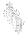
以下、本発明の第1の実施形態に係る半導体レーザ装置及びその製造方法について、図1及び図2を参照しながら説明する。尚、図1は第1の実施形態に係る半導体レーザ装置の斜視図であって、図2は図1におけるII−II線の断面図である。
【0066】
図1及び図2に示すように、n型GaAs基板100上の前方側の領域に、AlGaInP層を有し650nm帯の発振波長を持つ第1の半導体積層構造110が形成されていると共に、n型GaAs基板100上の後方側の領域に、AlGaAs層を有し780nm帯の発振波長を持つ第2の半導体積層構造120が形成されている。
【0067】
第1の半導体積層構造110は、n型GaAs基板100上の前方側の領域に下側から順次形成された、n型AlGaInP層からなるn型クラッド層111、AlGaInP層(障壁層)とGaInP層(井戸層)とが積層されてなる活性層112、p型AlGaInP層からなるp型の第1クラッド層113、n型AlInP層からなる一対の電流ブロック層114、p型AlGaInP層からなるp型の第2クラッド層115及びp型GaAs層からなるコンタクト層116により構成されている。第1の半導体積層構造110の上面には、例えばCr/Pt/Auの積層膜からなりコンタクト層116とオーミック接触する第1のp型電極117が形成されている。尚、活性層112は、レーザ光の発振波長が650nm帯になるように混晶の組成が選択されている。
【0068】
第2の半導体積層構造120は、n型GaAs基板100上の後方側の領域に下側から順次形成された、n型AlGaAs層からなるn型クラッド層121、AlGaAs層(障壁層)とGaAs層(井戸層)とが積層されてなる活性層122、p型AlGaAs層からなるp型の第1のクラッド層123、n型AlGaAs層からなる一対の電流ブロック層124、p型AlGaAs層からなるp型の第2のクラッド層125及びp型GaAs層からなるコンタクト層126により構成されている。第2の半導体積層構造120の上面には、例えばCr/Pt/Auの積層膜からなりコンタクト層126とオーミック接触する第2のp型電極127が形成されている。尚、活性層122は、レーザ光の発振波長が780nm帯になるように混晶の組成が選択されている。
【0069】
第1の半導体積層構造110及び第2の半導体積層構造120の下面には、例えばAu、Ge及びNiを含みn型GaAs基板100とオーミック接触するn型電極133が形成されている。
【0070】
第1の半導体積層構造110と第2の半導体積層構造120との接合部における上部には、光導波路の方向と直交する方向に延びる溝部134が形成されており、該溝部134によって、第1の半導体積層構造110のコンタクト層116及び第1のp型電極117と、第2の半導体積層構造120のコンタクト層126及び第2のp型電極127とが電気的に絶縁されている。
【0071】
第1の半導体積層構造110における一対の電流ブロック層114同士の間の領域の中心線と、第2の半導体積層構造120における一対の電流ブロック層124同士の間の領域の中心線とが一致していると共に、第1の半導体積層構造110のn型クラッド層111の厚さと第2の半導体積層構造120のn型クラッド層121の厚さとは等しく設定されている。これによって、第1の半導体積層構造110の活性層112のストライプ領域112aの中心線と、第2の半導体積層構造120の活性層122のストライプ領域122aの中心線とは一致している。
【0072】
第1の半導体積層構造110と第2の半導体積層構造120とは境界面135において互いに接合している。第1の半導体積層構造110の前端面である前方劈開面131には、酸化シリコン、窒化シリコン又は酸化アルミニウム等の誘電体膜からなる無反射コーティング層136が形成されていると共に、第2の半導体積層構造120の後端面である後方劈開面132には、酸化シリコン、窒化シリコン又は酸化アルミニウム等の誘電体膜とアモルファスシリコン膜とが積層されてなる高反射コーティング層137が形成されている。尚、図1においては、図示の都合上、無反射コーティング層136及び高反射コーティング層137は省略している。
【0073】
以下、第1の実施形態に係る半導体レーザ装置の動作について説明する。
【0074】
まず、第1のp型電極117から電流を注入すると、電流はp型の第2クラッド層115における一対の電流ブロック層114同士の間の領域に狭窄され、活性層112のストライプ領域112aにおいて650nm帯の発振波長を持つ第1のレーザ光が発振する。この場合、AlGaInP層のエネルギーギャップはAlGaAs層のエネルギーギャップよりも大きいため、AlGaAs層を有する活性層122は、AlGaInP層を有する活性層112から発振する第1のレーザ光に対する吸収係数が大きい。このため、第1のレーザ光は活性層112のストライプ領域112aにおいて前方劈開面131と境界面135とを共振器として発振するので、無反射コーティング層136が形成された前方劈開面131から650nm帯の波長を持つ第1のレーザ光が出射する。
【0075】
また、第2のp型電極127から電流を注入すると、電流はp型の第2クラッド層125における一対の電流ブロック層124同士の間の領域に狭窄され、活性層122のストライプ領域122aにおいて780nm帯の発振波長を持つ第2のレーザ光が発振する。この場合、第1の半導体積層構造110の活性層112のストライプ領域112aの中心線と第2の半導体積層構造120の活性層122のストライプ領域122aの中心線とが一致していると共に、AlGaInP層を有する活性層112は、第2のレーザ光に対する吸収係数が小さくて第2のレーザ光に対して透明であるから、第2のレーザ光は前方劈開面131と後方劈開面132とを共振器として発振する。また、後方劈開面132には高反射コーティング層137が形成されているので、前方劈開面131から780nm帯の波長を持つ第2のレーザ光が出射する。
【0076】
従って、前方劈開面131における1つの発光スポットから、波長が互いに異なる第1のレーザ光と第2のレーザ光とからなる2つのレーザ光を出射させることができる。
【0077】
尚、第1の実施形態においては、第1の半導体積層構造110はAlGaInP層を有し、第2の半導体積層構造120はAlGaAs層を有していたが、これに代えて、前方側に位置しAlGaN層を有する第1の半導体積層構造と、後方側に位置しAlGaInP層を有する第2の半導体積層構造とを組み合わせて、400nm帯の青紫色レーザ光及び650nm帯の赤色レーザ光を出射させてもよいし、前方側に位置しAlGaN層を有する第1の半導体積層構造と、後方側に位置しAlGaAs層を有する第2の半導体積層構造とを組み合わせて、400nm帯の青紫色レーザ光及び780nm帯の赤外レーザ光を出射させてもよい。尚、2波長の半導体レーザ装置においては、波長が短いレーザ光を出射する半導体積層構造をレーザ光の出射側に配置することが好ましい。
【0078】
以下、第1の実施形態に係る半導体レーザ装置の製造方法について説明する。
【0079】
まず、第1の製造方法としては、n型クラッド層111の厚さとn型クラッド層121の厚さとが等しい第1の半導体積層構造110及び第2の半導体積層構造120を別々に形成しておき、n型GaAs基板100上の前方側の領域に第1の半導体積層構造110を半田材等により接合すると共に、n型のGaAs基板100上の後方側の領域に第2の半導体積層構造120を半田材等により接合する。この場合、第1の半導体積層構造110における一対の電流ブロック層114同士の間の領域の中心線と、第2の半導体積層構造120における一対の電流ブロック層124同士の間の領域の中心線とを一致させる。このようにすると、第1の半導体積層構造110の活性層112のストライプ領域112aの中心線と、第2の半導体積層構造120の活性層122のストライプ領域122aの中心線とが一致する。尚、第1の製造方法においては、第1の半導体積層構造110及び第2の半導体積層構造120は、いずれも結晶成長させる必要が無いため、n型GaAs基板100に代えて、導電性の基板例えばシリコン基板を用いてもよい。
【0080】
第2の製造方法としては、n型GaAs基板100の上に全面に亘って第1の半導体積層構造110を形成すると共に、第2の半導体積層構造120を別途に形成しておき、第1の半導体積層構造110における後方側の領域をエッチングにより除去した後に、該後方側の領域に第2の半導体積層構造120を接合するか、又は、n型GaAs基板100の上に全面に亘って第2の半導体積層構造120を形成すると共に、第1の半導体積層構造110を別途に形成しておき、第2の半導体積層構造120における前方側の領域をエッチングにより除去した後に、該前方側の領域に第1の半導体積層構造110を接合する。
【0081】
(第2の実施形態)
以下、本発明の第2の実施形態に係る半導体レーザ装置について、図3を参照しながら説明する。
【0082】
図3に示すように、n型GaAs基板200上の前方側の領域に、AlGaN層を有し400nm帯の発振波長を持つ第1の半導体積層構造210が形成され、n型のGaAs基板200上の中央の領域に、AlGaInP層を有し650nm帯の発振波長を持つ第2の半導体積層構造220が形成され、n型のGaAs基板200上の後方側の領域に、AlGaAs層を有し780nm帯の発振波長を持つ第3の半導体積層構造230が形成されている。尚、図3においては、p型電極、コンタクト層及びn型電極を省略して示している。
【0083】
第1の半導体積層構造210は、レーザ光の発振波長が400nm帯になるように混晶の組成が選択された活性層211を有し、第2の半導体積層構造220は、レーザ光の発振波長が650nm帯になるように混晶の組成が選択された活性層221を有し、第3の半導体積層構造230は、レーザ光の発振波長が780nm帯になるように混晶の組成が選択された活性層231を有している。
【0084】
また、第1の半導体積層構造210における前方劈開面241には無反射コーティング層243が形成されていると共に、第3の半導体積層構造230における後方劈開面242には高反射コーティング層244が形成されている。
【0085】
第2の実施形態においては、第1の半導体積層構造210、第2の半導体積層構造220及び第3の半導体積層構造230の順につまり前方側から順に、活性層のエネルギーギャップが大きくなっているため、第1の半導体積層構造210の活性層211においては、400nm帯の波長を持つ青紫色レーザ光が前方劈開面241と第1の境界面245とを共振器として発振し、第2の半導体積層構造220の活性層221においては、650nm帯の波長を持つ赤色レーザ光が前方劈開面241と第2の境界面246とを共振器として発振し、第3の半導体積層構造230の活性層231においては、780nm帯の波長を持つ赤外レーザ光が前方劈開面241と後方劈開面242とを共振器として発振する。また、前方劈開面241に無反射コーティング層243が形成されていると共に、後方劈開面242に高反射コーティング層244が形成されているため、前方劈開面241から、400nm帯の波長を持つ青紫色レーザ光、650nm帯の波長を持つ赤色レーザ光及び780nm帯の波長を持つ赤外レーザ光がそれぞれ出射する。
【0086】
(第3の実施形態)
以下、本発明の第3の実施形態に係る半導体レーザ装置について、図4及び図5を参照しながら説明する。尚、図4は第3の実施形態に係る半導体レーザ装置斜視図であって、図5は図4におけるV−V線の断面図である。
【0087】
図4及び図5に示すように、n型GaAs基板300上の前方側の領域に、AlGaInP層を有し650nm帯の発振波長を持つ第1の半導体積層構造310が形成されていると共に、n型GaAs基板100上の後方側の領域に、AlGaAs層を有し780nm帯の発振波長を持つ第2の半導体積層構造320が形成されている。尚、第1の半導体積層構造310の後端部には、AlGaInP層を有する積層体からなる側壁成長部338が形成されている。
【0088】
第1の半導体積層構造310は、n型GaAs基板300上の前方側の領域に下側から順次形成された、n型AlGaInP層からなるn型クラッド層311、AlGaInP層(障壁層)とGaInP層(井戸層)とが積層されてなる活性層312、p型AlGaInP層からなるp型の第1クラッド層313、n型AlInP層からなる一対の電流ブロック層314、p型AlGaInP層からなるp型の第2クラッド層315及びp型GaAs層からなるコンタクト層316により構成されている。第1の半導体積層構造310の上面には、コンタクト層316とオーミック接触する第1のp型電極317が形成されている。尚、活性層312は、レーザ光の発振波長が650nm帯になるように混晶の組成が選択されている。
【0089】
第2の半導体積層構造320は、n型GaAs基板300上の後方側の領域に下側から順次形成された、n型AlGaAs層からなるn型クラッド層321、AlGaAs層(障壁層)とGaAs層(井戸層)とが積層されてなる活性層322、p型AlGaAs層からなるp型の第1クラッド層323、n型AlGaAs層からなる一対の電流ブロック層324、p型AlGaAs層からなるp型の第2クラッド層325及びp型GaAs層からなるコンタクト層326により構成されている。第2の半導体積層構造320の上面には、コンタクト層326とオーミック接触する第2のp型電極327が形成されている。尚、活性層322は、レーザ光の発振波長が780nm帯になるように混晶の組成が選択されている。
【0090】
第1の半導体積層構造310及び第2の半導体積層構造320の下面には、n型GaAs基板300とオーミック接触するn型電極333が形成されている。
【0091】
第1の半導体積層構造310と第2の半導体積層構造320とは境界面335において互いに接合している。第1の半導体積層構造310と第2の半導体積層構造320との接合部の上部には、光導波路が延びる方向と直交する方向に延びる溝部334が形成されており、該溝部334によって、第1の半導体積層構造310のコンタクト層316及び第1のp型電極317と、第2の半導体積層構造320のコンタクト層326及び第2のp型電極327とが電気的に絶縁されている。尚、側壁成長部338は溝部334の底面から突出している。
【0092】
第1の半導体積層構造310の前方劈開面331には無反射コーティング層336が形成されていると共に、第2の半導体積層構造320の後方劈開面332には高反射コーティング層337が形成されている。
【0093】
第1の半導体積層構造310における一対の電流ブロック層314同士の間の領域の中心線と、第2の半導体積層構造320における一対の電流ブロック層324同士の間の領域の中心線とが一致していると共に、第1の半導体積層構造310のn型クラッド層311の厚さと第2の半導体積層構造320のn型クラッド層321の厚さとは等しく設定されている。これによって、第1の半導体積層構造310の活性層312のストライプ領域312aの中心線と、第2の半導体積層構造320の活性層322のストライプ領域322aの中心線とは一致している。
【0094】
以下、第3の実施形態に係る半導体レーザ装置の動作について説明する。
【0095】
まず、第1のp型電極317から電流を注入すると、電流はp型の第2クラッド層315における一対の電流ブロック層314同士の間の領域に狭窄され、活性層の312のストライプ領域312aにおいて650nm帯の発振波長を持つ第1のレーザ光が発振する。この場合、第1のレーザ光は、活性層312のストライプ領域312aにおいて前方劈開面331と境界面335とを共振器として発振するが、側壁成長部338の幅寸法は共振器長に比べて非常に小さいため、側壁成長部338の影響は無視することができる。従って、無反射コーティング層336が形成されている前方劈開面331から650nm帯の波長を持つ第1のレーザ光が出射する。
【0096】
また、第2のp型電極327から電流を注入すると、電流はp型の第2クラッド層325における一対の電流ブロック層324同士の間の領域に狭窄され、活性層322のストライプ領域322aにおいて780nm帯の発振波長を持つ第1のレーザ光が発振する。第1の半導体積層構造310の活性層312のストライプ領域312aの中心線と、第2の半導体積層構造320の活性層322のストライプ領域322aの中心線とが一致していると共に、AlGaInP層を有する活性層312は、第2のレーザ光に対する吸収係数が小さくて第2のレーザ光に対して透明であるため、第2のレーザ光は前方劈開面331と後方劈開面332とを共振器として発振する。また、後方劈開面332には高反射コーティング層337が形成されているので、前方劈開面331から780nm帯の波長を持つ第2のレーザ光が出射する。
【0097】
従って、前方劈開面331における1つの発光スポットから、異なる波長を持つ第1のレーザ光及び第2のレーザ光よりなる2つのレーザ光を出射させることができる。
【0098】
尚、第3の実施形態においては、第1の半導体積層構造310はAlGaInP層を有し、第2の半導体積層構造320はAlGaAs層を有していたが、これに代えて、前方側に位置しAlGaN層を有する第1の半導体積層構造と、後方側に位置しAlGaInP層を有する第2の半導体積層構造とを組み合わせて、400nm帯の青紫色レーザ光及び650nm帯の赤色レーザ光を出射させてもよいし、前方側に位置しAlGaN層を有する第1の半導体積層構造と、後方側に位置しAlGaAs層を有する第2の半導体積層構造とを組み合わせて、400nm帯の青紫色レーザ光及び780nm帯の赤外レーザ光を出射させてもよい。尚、2波長の半導体レーザ装置においては、波長が短いレーザ光を出射する半導体積層構造をレーザ光の出射側に配置することが好ましい。
【0099】
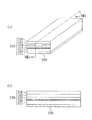
以下、第3の実施形態に係る半導体レーザ装置の製造方法について、図6(a)、(b)、図7(a)、(b)、図8(a)、(b)及び図9(a)、(b)、図10(a)、(b)及び図11(a)、(b)を参照しながら説明する。
【0100】
まず、図6(a)及び(b)に示すように、n型GaAs基板300の上に、MOCVD法又はMBE法により、n型AlGaAs層からなるn型クラッド層321、AlGaAs層とGaAs層とが積層されてなる活性層322、p型AlGaAs層からなるp型の第1クラッド層323及びn型AlGaAs層からなる電流ブロック層324を順次成長させる。
【0101】
次に、図7(a)及び(b)に示すように、フォトリソグラフィ及びエッチングにより、電流ブロック層324に光導波路方向に延びる溝部をp型の第1クラッド層323が露出するように形成した後、MOCVD法又はMBE法により、p型の第1クラッド層323及び一対の電流ブロック層324の上に、p型AlGaAs層からなるp型の第2クラッド層325及びp型GaAs層からなるコンタクト層326を順次成長させて、第1の暫定半導体積層構造340を形成する。
【0102】
次に、図8(a)及び(b)に示すように、第1の暫定半導体積層構造340における前方側の部分をn型GaAs基板300が露出するまでエッチングにより除去して、第1の暫定半導体積層構造340の後方側の部分からなる第2の半導体積層構造320を形成する。
【0103】
次に、図9(a)及び(b)に示すように、MOCVD法又はMBE法により、n型GaAs基板300における前方側の領域及び第2の半導体積層構造320の上に、n型クラッド層321と同じ厚さを持つn型のAlGaInP層からなるn型クラッド層311、AlGaInP層とGaInP層とが積層されてなる活性層312、p型AlGaInP層からなるp型の第1クラッド層313及びn型AlInP層からなる電流ブロック層314を順次成長させた後、電流ブロック層314に光導波路方向に延びる溝部をp型の第1クラッド層313が露出するように形成し、その後、再びMOCVD法又はMBE法を行なって、p型AlGaInP層からなるp型の第2クラッド層315及びp型GaAs層からなるコンタクト層316を成長させて、第2の暫定半導体積層構造350を形成する。
【0104】
次に、図10(a)及び(b)に示すように、第2の暫定半導体積層構造350における第2の半導体積層構造320よりも上側部分をエッチングにより除去して、第2の暫定半導体積層構造350の前方側の部分からなる第1の半導体積層構造310を形成する。このようにすると、第1の半導体積層構造310における第2の半導体積層構造320側の後端部に、AlGaInPを有する積層体からなる側壁成長部338が残存する。尚、側壁成長部338は、第2の半導体積層構造320の前端面との間における、結晶成長面の面方位の相違から極めて薄くにしか形成されない。
【0105】
次に、図11(a)及び(b)に示すように、第1の半導体積層構造310のコンタクト層316と第2の半導体積層構造320のコンタクト層326との接合部に、光導波路が延びる方向と直交する方向に延びる溝部334を形成した後、コンタクト層316の上に第1のp型電極317を形成し且つコンタクト層326の上に第2のp型電極327を形成する。また、n型GaAs基板300の下面にn型電極333を形成する。その後、第1の半導体積層構造310の前方劈開面331に無反射コーティング層336を形成すると共に、第2の半導体積層構造320の後方劈開面332に高反射コーティング層337を形成する。
【0106】
尚、第3の実施形態に係る半導体レーザ装置の製造方法においては、n型GaAs基板300上に全面に亘って、第2の半導体積層構造320と同じ積層構造を有する第1の暫定半導体積層構造340を成長させた後、該第1の暫定半導体積層構造340の前方側の部分を除去して、n型GaAs基板300上の後方側の領域に第2の半導体積層構造320を形成し、次に、n型GaAs基板300上の前方側の領域及び第2の半導体積層構造320の上に全面に亘って、第1の半導体積層構造310と同じ積層構造を有する第2の暫定半導体積層構造350を成長させた後、該第2の暫定半導体積層構造350における第2の半導体積層構造320よりも上側の部分を除去して、n型GaAs基板300上の前方側の領域に第1の半導体積層構造310を形成したが、これに代えて、n型GaAs基板300上に全面に亘って、第1の半導体積層構造310と同じ積層構造を有する第1の暫定半導体積層構造を成長させた後、該第1の暫定半導体積層構造の後方側の部分を除去して、n型GaAs基板300上の前方側の領域に第1の半導体積層構造310を形成し、次に、n型GaAs基板300上の後方側の領域及び第1の半導体積層構造310の上に全面に亘って、第2の半導体積層構造320と同じ積層構造を有する第2の暫定半導体積層構造を成長させた後、該第2の暫定半導体積層構造における第1の半導体積層構造310よりも上側の部分を除去して、n型GaAs基板300上の後方側の領域に第2の半導体積層構造320を形成してもよい。
【0107】
(第3の実施形態の第1変形例)
以下、本発明の第3の実施形態の第1変形例に係る半導体レーザ装置について、図12及び図13を参照しながら説明する。尚、図12は第3の実施形態の第1変形例に係る半導体レーザ装置の斜視図であって、図13は図12におけるXIII−XIII線の断面図である。
【0108】
尚、第3の実施形態の第1変形例においては、図4及び図5を参照しながら説明した第3の実施形態と同一の部材については同一の符号を付すことにより、説明を省略する。
【0109】
第3の実施形態の第1変形例の特徴として、図12及び図13に示すように、側壁成長部338は溝部334の底面から突出しておらず、側壁成長部338の上面と溝部334の底面とが面一である。
【0110】
側壁成長部338における溝部334の底面から突出する部分は、第1の半導体積層構造310のコンタクト層316と第2の半導体積層構造320のコンタクト層326との接合部に溝部334を形成する工程(図11(a)、(b)を参照)においてエッチングにより除去されている。
【0111】
(第3の実施形態の第2変形例)
以下、第3の実施形態の第2変形例に係る半導体レーザ装置及びその製造方法について、図14(a)及び(b)を参照しながら説明する。尚、図14(a)は第3の実施形態の第2変形例に係る半導体レーザ装置の斜視図であり、図14(b)は図14(a)におけるXIVb−XIVb線の断面図である。
【0112】
尚、第3の実施形態の第2変形例においては、図4及び図5を参照しながら説明した第3の実施形態と同一の部材については同一の符号を付すことにより、説明を省略する。
【0113】
第3の実施形態の第2変形例の特徴として、図14(a)及び(b)に示すように、第1の半導体積層構造310と第2の半導体積層構造320との接合部には、光導波路の方向と直交する方向に延び且つT字状の断面を有する溝部334Aが形成されており、該溝部334Aには、屈折率整合樹脂、酸化シリコン又は窒化シリコン等からなる誘電体部材339が充填されている。これにより、第1の半導体積層構造310と第2の半導体積層構造320とが電気的に絶縁されている。
【0114】
ところで、赤色レーザ光を発振する第1の半導体積層構造310は、赤外レーザ光を発振する第2の半導体積層構造320よりも発振のしきい値電流が大きいため、第1の半導体積層構造310の動作時には、第1の半導体積層構造310から第2の半導体積層構造320に、僅かではあるが無効電流が流れる恐れがある。しかしながら、第2変形例においては、第1の半導体積層構造310と第2の半導体積層構造320との接合部に絶縁性の誘電体部材339が介在しているため、無効電流が流れなくなる。
【0115】
誘電体部材339の屈折率としては、第1の半導体積層構造310における活性層312のストライプ領域312aの実効屈折率と、第2の半導体積層構造320における活性層322のストライプ領域322aの実効屈折率との間の値であることが好ましい。
【0116】
このようにすると、第1の半導体積層構造310の活性層312から出射される第1のレーザ光と第2の半導体積層構造320の活性層322との光の結合効率が向上すると共に、第2の半導体積層構造320の活性層322から出射される第2のレーザ光と第1の半導体積層構造310の活性層312との光の結合効率が向上するため、半導体レーザ装置の光学的特性が向上する。
【0117】
尚、第3の実施形態の第2変形例に係る半導体レーザ装置を製造するには、第1の半導体積層構造310のコンタクト層316と第2の半導体積層構造320のコンタクト層326との接合部に溝部334を形成した後(図13を参照)、側壁成長部338をエッチングにより除去してT字状の溝部334Aを形成し、その後、T字状の溝部334Aに誘電体部材339を充填する。
【0118】
(第4の実施形態)
本発明の第4の実施形態に係る半導体レーザ装置について、図15(a)及び(b)を参照しながら説明する。尚、図15(a)は第4の実施形態に係る半導体レーザ装置の斜視図であり、図15(b)は図15(a)におけるXVb−XVb線の断面図である。
【0119】
図15(a)及び(b)に示すように、n型GaAs基板400上の前方側の領域には、AlGaInP層を有し650nm帯の発振波長を持つ第1の半導体積層構造410が形成されており、n型GaAs基板400上の後方側の領域には、AlGaAs層を有し780nm帯の発振波長を持つ第2の半導体積層構造420が形成されている。
【0120】
第1の半導体積層構造410は、n型GaAs基板400上におけるレーザ光の出射方向の前方側の領域に順次形成された、n型AlGaInP層からなるn型クラッド層411、AlGaInP層(障壁層)とGaInP層(井戸層)とが積層されてなる活性層412、p型AlGaInP層からなる第1のp型クラッド層413、一対のn型AlInP層からなる電流ブロック層414、p型AlGaInP層からなる第2のp型クラッド層415及びp型GaAs層からなるコンタクト層416により構成されている。コンタクト層416の上面には、該コンタクト層416とオーミック接触する第1のp側電極417が形成されている。活性層412はレーザ光の発振波長がほぼ650nm帯となるように混晶の組成が設定されている。
【0121】
第2の半導体積層構造420は、n型GaAs基板400上におけるレーザ光の出射方向の後方側の領域に順次形成された、n型AlGaAs層からなるn型クラッド層421、AlGaAs層(障壁層)とGaAs層(井戸層)とが積層されてなる活性層422、p型AlGaAs層からなる第1のp型クラッド層423、一対のn型AlGaAs層からなる電流ブロック層424、p型AlGaInP層からなる第2のp型クラッド層425及びp型GaAs層からなるコンタクト層426により構成されている。コンタクト層426の上面には、該コンタクト層426とオーミック接触する第2のp側電極427が第1のp側電極417と間隔をおいて形成されている。活性層422はレーザ光の発振波長がほぼ780nm帯となるように混晶の組成が設定されている。
【0122】
n型GaAs基板400の下面には、該基板400とオーミック接触するn側電極433が形成されている。
【0123】
第1の半導体積層構造410における活性層412の前方劈開面431には、酸化シリコン、窒化シリコン又は酸化アルミニウム等の誘電体膜からなる無反射コート膜436が形成されている。第2の半導体積層構造420における活性層422の後方劈開面432には、酸化シリコン、窒化シリコン又は酸化アルミニウム等の誘電体膜とアモルファスシリコン等とが積層されてなる高反射コート膜437が形成されている。
【0124】
第4の実施形態の第1の特徴として、第1の半導体積層構造410のn型クラッド層411の厚さは、第2の半導体積層構造420のn型クラッド層421の厚さよりも大きい。これにより、第1の半導体積層構造410の活性層412のストライプ領域412aは、第2の半導体積層構造420の活性層422のストライプ領域422aよりも上側に位置している。
【0125】
より具体的には、第1の半導体積層構造410のn型クラッド層411の膜厚は、第2の半導体積層構造420のn型クラッド層421、活性層422及び第1のp型クラッド層423の合計厚さよりも大きく、且つ、第1の半導体積層構造410のn型クラッド層411、活性層412及び第1のp型クラッド層413の合計厚さは、第2の半導体積層構造420のn型クラッド層421、活性層422、第1のp型クラッド層423及び第2のp型クラッド層425の合計厚さよりも小さい。その結果、第1の半導体積層構造410の活性層412のストライプ領域412aの後端面は、第2の半導体積層構造420の第2のp型クラッド層425の前端面と接合する。
【0126】
第4の実施形態の第2の特徴として、第1の半導体積層構造410の第2のp型クラッド層415と、第2の半導体積層構造420の第2のp型クラッド層425との組成は同一である。
【0127】
以下、第4の実施形態に係る半導体レーザ装置の動作を説明する。
【0128】
まず、第1のp側電極417から電流を注入すると、注入された電流は第2のp型クラッド層415における一対の電流ブロック層414同士の間の領域に狭窄され、ストライプ領域412aにおいて650nm帯の発振波長を持つ第1のレーザ光が発振する。
【0129】
第1の半導体積層構造410の第2のp型クラッド層415の組成と第2の半導体積層構造420の第2のp型クラッド層425の組成とが同一であるため、境界面435においては、屈折率及び吸収係数の差に起因するレーザ光の反射は生じない。このため、第1のレーザ光は、前方劈開面431と後方劈開面432とを実質的な共振器として発振し、無反射コート膜436が形成されている前方劈開面431から650nm帯の波長を持つレーザ光として出射する。
【0130】
このように、第2の半導体積層構造420の第2のp型クラッド層425のエネルギーギャップは、第1の半導体積層構造410の活性層412のエネルギーギャップよりも大きいため、第2のp型クラッド層425は第1のレーザ光に対して透明になるので、第2の半導体積層構造420において光吸収損失は生じない。
【0131】
尚、第4の実施形態においては、第1の半導体積層構造410の第2のp型クラッド層415の組成と、第2の半導体積層構造420の第2のp型クラッド層425の組成とを同一にしたが、これに限らず、第2のp型クラッド層425のエネルギーギャップを、第1の半導体積層構造410の活性層412のエネルギーギャップよりも大きくなるようにすればよい。
【0132】
また、第2のp側電極427から電流を注入すると、注入された電流は第2のp型クラッド層425における一対の電流ブロック層424同士の間の領域に狭窄され、ストライプ領域422aにおいて780nm帯の発振波長を持つ第2のレーザ光が発振する。
【0133】
第2の半導体積層構造420の活性層422のストライプ領域422aの前端面は、第1の半導体積層構造410のn型クラッド層411の後方面と接合している。また、n型AlGaInP層からなるn型クラッド層411は第2のレーザ光に対して透明であるため、第2のレーザ光は、前方劈開面431と後方劈開面432とを共振器として発振する。また、後方劈開面432には高反射コート膜437が形成されているので、前方劈開面431から780nm帯の波長を持つ第2のレーザ光が出射する。
【0134】
従って、第4の実施形態によると、前方劈開面431における活性層412のストライプ領域412aが第1のレーザ光の発光スポットとなり、前方劈開面431における活性層412のストライプ領域412aの下側に第2の発光スポットが形成されるため、上下に近接する2つの発光スポットを有する2波長の半導体レーザ装置が実現できる。この場合、第1の発光スポットと第2の発光スポットとのピッチは、第1の半導体積層構造と第2の半導体積層構造とが横方向に並列される2波長の半導体レーザ装置における発光スポットのピッチに比べると、極めて小さい。
【0135】
尚、第4の実施形態においては、第1の半導体積層構造410の活性層412の基板面からの位置は、第2の半導体積層構造420の活性層422の基板面からの位置よりも上であったが、これに代えて、第2の半導体積層構造420の活性層422の位置を、第1の半導体積層構造410の活性層412の位置よりも上にしてもよい。この場合には、第2の半導体積層構造420における第1の半導体積層構造410の活性層412と対向する半導体層の組成を、第1の半導体積層構造410のn型クラッド層411とほぼ同一にすればよい。
【0136】
また、第4の実施形態においては、第1の半導体積層構造410はAlGaInP層を有し、第2の半導体積層構造420はAlGaAs層を有していたが、これに代えて、前方側に位置しAlGaN層を有する第1の半導体積層構造と、後方側に位置しAlGaInP層を有する第2の半導体積層構造とを組み合わせて、400nm帯の青紫色レーザ光及び650nm帯の赤色レーザ光を出射させてもよいし、前方側に位置しAlGaN層を有する第1の半導体積層構造と、後方側に位置しAlGaAs層を有する第2の半導体積層構造とを組み合わせて、400nm帯の青紫色レーザ光及び780nm帯の赤外レーザ光を出射させてもよい。尚、2波長の半導体レーザ装置においては、波長が短いレーザ光を出射する半導体積層構造をレーザ光の出射側に配置することが好ましい。
【0137】
以下、第4の実施形態に係る半導体レーザ装置の製造方法について説明する。
【0138】
第1の製造方法は、n型クラッド層411の厚さがn型クラッド層421の厚さよりも大きくなるように、第1の半導体積層構造410及び第2の半導体積層構造420を別々に作製しておく。その後、n型GaAs基板400上の前方側の領域に第1の半導体積層構造410を半田材等により固着すると共に、n型GaAs基板400上の後方側の領域に第2の半導体積層構造420を半田材等により固着すると共に、第1の半導体積層構造410と第2の半導体積層構造420とを境界面435で接合する。この場合、第1の半導体積層構造410の活性層412のストライプ領域412aの中心線と、第2の半導体積層構造420の活性層422のストライプ領域422aの中心線とを一致させる。尚、第1の製造方法においては、第1及び第2の半導体積層構造410、420はn型GaAs基板400の上に結晶成長させる必要がないので、n型GaAs基板400に代えて、導電性の基板を用いてもよい。
【0139】
第2の製造方法は、n型GaAs基板400の上に全面に亘って第1の半導体積層構造410を形成すると共に、第2の半導体積層構造420を別途に形成しておき、第1の半導体積層構造410における後方側の領域をエッチングにより除去した後に、該後方側の領域に第2の半導体積層構造420を接合するか、又は、n型GaAs基板400の上に全面に亘って第2の半導体積層構造420を形成すると共に、第1の半導体積層構造410を別途に形成しておき、第2の半導体積層構造420における前方側の領域をエッチングにより除去した後に、該前方側の領域に第1の半導体積層構造410を接合する。この場合、第1の半導体積層構造410の活性層412のストライプ領域412aの中心線と、第2の半導体積層構造420の活性層422のストライプ領域422aの中心線とを一致させる。
【0140】
(第5の実施形態)
以下、本発明の第5の実施形態に係る半導体レーザ装置について、図16(a)及び(b)を参照しながら説明する。尚、図16(a)は第5の実施形態に係る半導体レーザ装置の斜視図であり、図16(b)は図16(a)におけるXVIb−XVIb線の断面図である。
【0141】
図16(a)及び(b)に示すように、例えば、導電性を持つシリコンからなる基板500上におけるレーザ光の出射方向の前方側の領域に、AlGaInP層を有し650nm帯の発振波長を持つ第1の半導体積層構造510が設けられ、基板500上におけるレーザ光の出射方向の後方側の領域に、AlGaAs層を有し780nm帯の発振波長を持つ第2の半導体積層構造520が第1の半導体積層構造510との間に空隙部534を介して設けられている。
【0142】
第1の半導体積層構造510は、レーザ光の発振波長が650nm帯となるように混晶の組成が設定された活性層512を有しており、第1の半導体積層構造510の前端面には無反射コート膜536が形成されていると共に、第1の半導体積層構造510の後端面には、無反射コート膜536よりも反射率が大きい第1の端面コート膜538が形成されている。
【0143】
第2の半導体積層構造520は、レーザ光の発振波長が780nm帯となるように混晶の組成が設定された活性層522を有しており、第2の半導体積層構造520の後端面には高反射コート膜537が形成されていると共に、第2の半導体積層構造520の前端面には高反射コート膜537よりも反射率が小さい第2の端面コート膜539が形成されている。
【0144】
第5の実施形態においては、第1の半導体積層構造510における一対の電流ブロック層同士の間の領域の中心線と、第2の半導体積層構造520における一対の電流ブロック層同士の間の領域の中心線とが一致していると共に、第1の半導体積層構造510のn型クラッド層の厚さと第2の半導体積層構造520のn型クラッド層の厚さとは等しく設定されている。これにより、第1の半導体積層構造510の活性層512のストライプ領域の中心線と、第2の半導体積層構造520の活性層522のストライプ領域の中心線とは一致している。
【0145】
以下、第5の実施形態に係る半導体レーザ装置の動作について説明する。
【0146】
まず、第1の半導体積層構造510に電流を注入した場合には、第1の半導体積層構造510の活性層512において650nm帯の発振波長を持つ第1のレーザ光が、活性層512における無反射コート膜536と第1の端面コート膜538とを共振器端面として発振して、無反射コート膜536から出射する。
【0147】
また、第2の半導体積層構造520に電流を注入した場合は、第2の半導体積層構造520の活性層522において780nm帯の発振波長を持つ第2のレーザ光が、活性層522における第2の端面コート膜539と高反射コート膜537とを共振器端面として発振して、第2の端面コート膜539から出射する。
【0148】
従って、第5の実施形態によると、第2のレーザ光は第1の半導体積層構造510の活性層512からなるストライプ状の光導波路を伝播し、無反射コート膜536における、第1の半導体積層構造510の光導波路により決定される発光スポットから出射する。その結果、1つの発光スポットから、第1のレーザ光及び第2のレーザ光が出射する2波長の半導体レーザ装置を実現できる。
【0149】
尚、第5の実施形態においては、第1の半導体積層構造510の活性層512のストライプ領域の中心線と、第2の半導体積層構造520の活性層522のストライプ領域の中心線とが一致している場合について説明したが、第4の実施形態のように、第1の半導体積層構造510の活性層512のストライプ領域の中心線が、第2の半導体積層構造520の活性層522のストライプ領域の中心線に対して上側又は下側に位置していてもよい。この場合でも、前方側に位置する第1の半導体積層構造510が、第2のレーザ光に対して透明であれば、上下に位置し且つ互いに近接する2つの発光スポットから、互いに波長が異なる2つのレーザ光を発振させることができる。
【0150】
尚、第5の実施形態においては、第1の半導体積層構造510はAlGaInP層を有し、第2の半導体積層構造520はAlGaAs層を有していたが、これに代えて、前方側に位置しAlGaN層を有する第1の半導体積層構造と、後方側に位置しAlGaInP層を有する第2の半導体積層構造とを組み合わせて、400nm帯の青紫色レーザ光及び650nm帯の赤色レーザ光を出射させてもよいし、前方側に位置しAlGaN層を有する第1の半導体積層構造と、後方側に位置しAlGaAs層を有する第2の半導体積層構造とを組み合わせて、400nm帯の青紫色レーザ光及び780nm帯の赤外レーザ光を出射させてもよい。尚、2波長の半導体レーザ装置においては、波長が短いレーザ光を出射する半導体積層構造をレーザ光の出射側に配置することが好ましい。
【0151】
以下、第5の実施形態に係る半導体レーザ装置の製造方法について説明する。
【0152】
まず、前端面に無反射コート膜536を有し且つ後端面に無反射コート膜536よりも反射率が大きい第1の端面コート膜538を有するチップ状の第1の半導体積層構造(第1のレーザチップ)510と、後端面に高反射コート膜537を有し且つ前端面に高反射コート膜537よりも反射率が小さい第2の端面コート膜539を有するチップ状の第2の半導体積層構造(第2のレーザチップ)520とをそれぞれ作製しておく。
【0153】
次に、基板500上の前方側の領域に第1の半導体積層構造510を半田材等により固着すると共に、基板500上の後方側の領域に第2の半導体積層構造520を第1の半導体積層構造510との間に空隙部534ができるように半田材等により固着する。この場合に、第1の半導体積層構造510の活性層512のストライプ領域の中心線と、第2の半導体積層構造520の活性層522のストライプ領域の中心線とを一致させる。
【0154】
(第5の実施形態の変形例)
以下、第5の実施形態の一変形例に係る半導体レーザ装置について図17を参照しながら説明する。図17は第5の実施形態の一変形例に係る半導体レーザ装置の斜視図である。
【0155】
尚、第5の実施形態の変形例においては、図16(a)及び(b)を参照しながら説明した第5の実施形態と同一の部材については同一の符号を付すことにより、説明を省略する。
【0156】
第5の実施形態の変形例の特徴として、図17に示すように、基板500の上における第1の半導体積層構造510と第2の半導体積層構造520との間の空隙部534には、屈折率整合樹脂、酸化シリコン又は窒化シリコン等からなる誘電体部材540が充填されており、該誘電体部材540の屈折率は、第1の半導体積層構造510における活性層512のストライプ領域の実効屈折率と、第2の半導体積層構造520における活性層522のストライプ領域の実効屈折率との間の値を有している。
【0157】
従って、第1の半導体積層構造510と第2の半導体積層構造520とが誘電体部材540により電気的に絶縁されている。また、第1の半導体積層構造510の活性層512から出射される第1のレーザ光と第2の半導体積層構造520の活性層522との光の結合効率が向上するため、半導体レーザ装置の光学的特性が向上する。
【0158】
(第6の実施形態)
以下、本発明の第6の実施形態に係る半導体レーザ装置について、図18を参照しながら説明する。図18は第6の実施形態に係る半導体レーザ装置の断面図である。
【0159】
図18に示すように、第6の実施形態に係る半導体レーザ装置は、導電性を持つシリコンからなる基板600上におけるレーザ光の出射方向の前方側の領域から後方側の領域に順次設けられ、AlGaInN層を有し発振波長が400nm帯である第1の半導体積層構造610と、AlGaInP層を有し発振波長が650nm帯である第2の半導体積層構造620と、AlGaAs層を有し発振波長が780nm帯である第3の半導体積層構造630とを有している。
【0160】
第1の半導体積層構造610は、レーザ光の発振波長が400nm帯となるように混晶の組成が設定された活性層612を有しており、第1の半導体積層構造610の前端面には無反射コート膜636が形成されている。第2の半導体積層構造620は、レーザ光の発振波長が650nm帯となるように混晶の組成が設定された活性層622を有している。第3の半導体積層構造630は、レーザ光の発振波長が780nm帯となるように混晶の組成が設定された活性層632を有しており、第3の半導体積層構造630の後端面には高反射コート膜637が形成されている。
【0161】
基板600上における第1の半導体積層構造610と第2の半導体積層構造620との間には、屈折率整合樹脂、酸化シリコン又は窒化シリコン等からなる第1の誘電体部材638が充填されている。第1の誘電体部材638の屈折率は、第1の半導体積層構造610における活性層612のストライプ領域の実効屈折率と、第2の半導体積層構造620における活性層622のストライプ領域の実効屈折率との間の値である。
【0162】
基板600上における第2の半導体積層構造620と第3の半導体積層構造630との間には、屈折率整合樹脂、酸化シリコン又は窒化シリコン等からなる第2の誘電体部材639が充填されている。第2の誘電体部材639の屈折率は、第2の半導体積層構造620における活性層622のストライプ領域の実効屈折率と、第3の半導体積層構造630における活性層632のストライプ領域の実効屈折率との間の値である。
【0163】
第1の半導体積層構造610における一対の電流ブロック層同士の間の領域の中心線と、第2の半導体積層構造620における一対の電流ブロック層同士の間の領域の中心線とが一致していると共に、第1の半導体積層構造610のn型クラッド層の厚さと第2の半導体積層構造620のn型クラッド層の厚さとは等しく設定されている。また、第2の半導体積層構造620における一対の電流ブロック層同士の間の領域の中心線と、第3の半導体積層構造630における一対の電流ブロック層同士の間の領域の中心線とが一致していると共に、第2の半導体積層構造620のn型クラッド層の厚さと第3の半導体積層構造630のn型クラッド層の厚さとは等しく設定されている。
【0164】
これらにより、第1の半導体積層構造610の活性層612のストライプ領域の中心線、第2の半導体積層構造620の活性層622のストライプ領域の中心線、及び第3の半導体積層構造630の活性層632のストライプ領域の中心線は互いに一致している。
【0165】
以下、第6の実施形態に係る半導体レーザ装置の動作について説明する。
【0166】
まず、第1の半導体積層構造610に電流を注入した場合には、第2の半導体積層構造620は、第1の半導体積層構造610の活性層612のストライプ領域から発振し400nm帯の発振波長を持つ第1のレーザ光に対する吸収係数が大きいため、第1のレーザ光は第2の半導体積層構造620の内部に伝播し難い。このため、第1のレーザ光は、無反射コート膜636と第1の誘電体部材638とを共振器端面として発振して、無反射コート膜636から出射する。
【0167】
次に、第2の半導体積層構造620に電流を注入した場合には、第1の半導体積層構造610は、第2の半導体積層構造620の活性層622のストライプ領域から発振し650nm帯の発振波長を持つ第2のレーザ光に対する吸収係数が小さくて第2のレーザ光に対して透明であり、また、第3の半導体積層構造630は第2のレーザ光に対する吸収係数が大きいから、第2のレーザ光は第3の半導体積層構造630の内部に伝播し難い。このため、第2のレーザ光は、第1の半導体積層構造610の前端面と第2の半導体積層構造620とを共振器として発振し、無反射コート膜636側から出射する。
【0168】
また、第3の半導体積層構造630に電流を注入した場合は、第3の半導体積層構造630の活性層632における780nm帯の発振波長を持つ第3のレーザ光に対して、第1の半導体積層構造610及び第2の半導体積層構造620は共に吸収係数が小さくて第3のレーザ光に対して透明であるから、第3のレーザ光は、無反射コート膜636と第2の誘電体部材639とを共振器として発振し、無反射コート膜636から出射する。
【0169】
従って、第6の実施形態によると、第2のレーザ光は第1の半導体積層構造610の活性層612からなるストライプ状の光導波路を伝播して、無反射コート膜636における発光スポットから出射する。また、第3のレーザ光は、第1の半導体積層構造610の活性層612からなるストライプ状の光導波路及び第2の半導体積層構造620の活性層622からなるストライプ状の光導波路を伝播して、無反射コート膜636における発光スポットから出射する。その結果、第2のレーザ光及び第3のレーザ光は、第1のレーザ光と同じ発光スポットから出射するので、波長が異なる3つのレーザ光が1つの発光スポットから出射する3波長の半導体レーザ装置を実現できる。
【0170】
尚、第6の実施形態においては、第1の半導体積層構造610の活性層612のストライプ領域の中心線、第2の半導体積層構造620の活性層622のストライプ領域の中心線及び第3の半導体積層構造630の活性層632のストライプ領域の中心線は互いに一致していたが、これに代えて、第1の半導体積層構造610の活性層612のストライプ領域の中心線と、第2の半導体積層構造620の活性層622のストライプ領域の中心線とを上下方向にオフセットさせる一方、第3の半導体積層構造630の活性層632のストライプ領域の中心線を、第1の半導体積層構造610の活性層612のストライプ領域の中心線又は第2の半導体積層構造620の活性層622のストライプ領域の中心線と一致させてもよい。このようにすると、上下方向に位置する2つの発光スポットから、波長が異なる3つのレーザ光が出射する3波長の半導体レーザ装置を実現できる。
【0171】
以下、第6の実施形態に係る半導体レーザ装置の製造方法について、図18、図19(a)〜(c)及び図20を参照しながら説明する。
【0172】
まず、図18に示すような、前端面に無反射コート膜636が形成されたチップ状の第1の半導体積層構造610(第1のレーザチップ)と、チップ状の第2の半導体積層構造620(第2のレーザチップ)と、後端面に高反射コート膜637が形成されたチップ状の第3の半導体積層構造630(第3のレーザチップ)とを、MOVPE法等のエピタキシャル成長法、リソグラフィ法及びエッチング法等の微細加工法を用いて作製しておく。
【0173】
次に、図19(a)に示すように、基板600上の前方側の領域に第1の半導体積層構造610を半田材等によって固着する。
【0174】
次に、図19(b)に示すように、基板600上における第1の半導体積層構造610の後方側の領域(中央の領域)に第2の半導体積層構造620を第1の半導体積層構造610との間に間隔をおいて半田材等によって固着する。この場合、第1の半導体積層構造610の活性層612のストライプ領域の中心線と、第2の半導体積層構造620の活性層622のストライプ領域の中心線とを一致させる。
【0175】
次に、図19(c)に示すように、基板600上における第2の半導体積層構造620の後方側の領域に第3の半導体積層構造630を第2の半導体積層構造620との間に間隔をおいて半田材等によって固着する。この場合、第2の半導体積層構造620の活性層622のストライプ領域の中心線と、第3の半導体積層構造630の活性層632のストライプ領域の中心線とを一致させる。
【0176】
尚、基板600上の前方側の領域に第1の半導体積層構造610が固着され、基板600上における中央の領域に第2の半導体積層構造620が固着され、基板600上における後方側の領域に第3の半導体積層構造630が固着されるならば、第1、第2及び第3の半導体積層構造610、620、630を固着する順序については問わない。
【0177】
次に、図20に示すように、基板600上における第1の半導体積層構造610と第2の半導体積層構造620との間に第1の誘電体部材638を充填すると共に、基板600上における第2の半導体積層構造620と第3の半導体積層構造630との間に第2の誘電体部材639を充填する。
【0178】
【発明の効果】
本発明に係る半導体レーザ装置によると、波長が異なる第1及び第2のレーザ光を、前方側の領域に設けられている第1の半導体積層構造の前端面における、1つの発光スポット又は極めて接近した2つの発光スポットから出射させることができるので、波長が異なる複数のレーザ光を、光ディスクの微少なスポットに確実に集光できると共に1つのフォトディテクタにより検出することができる。
【0179】
本発明に係る第1又は第2の半導体レーザ装置の製造方法によると、基板上の前方側の領域に第1のレーザ光を発振させる第1の半導体積層構造が設けられ且つ基板上の後方側の領域に第2のレーザ光を発振させる第2の半導体積層構造が設けられていると共に、第1のレーザ光の出射方向と第2のレーザ光の出射方向とが同方向であるモノリシック型の半導体レーザ装置を確実に製造することができる。
【0180】
本発明に係る第3の半導体レーザ装置の製造方法によると、基板上の前方側の領域に第1のレーザ光を発振させる第1のレーザチップが設けられ且つ基板上の後方側の領域に第2のレーザ光を発振させる第2のレーザチップが設けられていると共に、第1のレーザ光の出射方向と第2のレーザ光の出射方向とが同方向であるハイブリッド型の2波長半導体レーザ装置を確実に製造することができる。
【0181】
本発明に係る第4の半導体レーザ装置の製造方法によると、基板上の前方側の領域に第1のレーザ光を発振させる第1のレーザチップが設けられ、基板上の中央の領域に第2のレーザ光を発振させる第2のレーザチップが設けられ且つ基板上の後方側の領域に第3のレーザ光を発振させる第3のレーザチップが設けられていると共に、第1のレーザ光の出射方向と第2のレーザ光の出射方向と第3のレーザ光の出射方向とが同方向であるハイブリッド型の3波長半導体レーザ装置を確実に製造することができる。
【図面の簡単な説明】
【図1】第1の実施形態に係る半導体レーザ装置の斜視図である。
【図2】第1の実施形態に係る半導体レーザ装置を示し、図1におけるII−II線の断面図である。
【図3】第2の実施形態に係る半導体レーザ装置の断面図である。
【図4】第3の実施形態に係る半導体レーザ装置の斜視図である。
【図5】第3の実施形態に係る半導体レーザ装置を示し、図4におけるV−V線の断面図である。
【図6】(a)及び(b)は第3の実施形態に係る半導体レーザ装置の製造方法の一工程を示し、(a)は斜視図であって、(b)は(a)におけるVIb−VIb線の断面図である。
【図7】(a)及び(b)は第3の実施形態に係る半導体レーザ装置の製造方法の一工程を示し、(a)は斜視図であって、(b)は(a)におけるVIIb−VIIb線の断面図である。
【図8】(a)及び(b)は第3の実施形態に係る半導体レーザ装置の製造方法の一工程を示し、(a)は斜視図であって、(b)は(a)におけるVIIIb−VIIIb線の断面図である。
【図9】(a)及び(b)は第3の実施形態に係る半導体レーザ装置の製造方法の一工程を示し、(a)は斜視図であって、(b)は(a)におけるIXb−IXb線の断面図である。
【図10】(a)及び(b)は第3の実施形態に係る半導体レーザ装置の製造方法の一工程を示し、(a)は斜視図であって、(b)は(a)におけるXb−Xb線の断面図である。
【図11】(a)及び(b)は第3の実施形態に係る半導体レーザ装置の製造方法の一工程を示し、(a)は斜視図であって、(b)は(a)におけるXIb−XIb線の断面図である。
【図12】第3の実施形態の第1変形例に係る半導体レーザ装置の斜視図である。
【図13】第3の実施形態の第1変形例に係る半導体レーザ装置を示し、図12におけるXIII−XIII線の断面図である。
【図14】(a)及び(b)は第3の実施形態の第2変形例に係る半導体レーザ装置を示し、(a)は斜視図であり、(b)は(a)におけるXIVb−XIVb線の断面図である。
【図15】(a)及び(b)は第4の実施形態に係る半導体レーザ装置を示し、(a)は斜視図であり、(b)は(a)におけるXVb−XVb線の断面図である。
【図16】(a)及び(b)は第5の実施形態に係る半導体レーザ装置を示し、(a)は斜視図であり、(b)は(a)におけるXVIb−XVIb線の断面図である。
【図17】第5の実施形態の一変形例に係る半導体レーザ装置の斜視図である。
【図18】第6の実施形態に係る半導体レーザ装置の断面図である。
【図19】(a)〜(c)は第6の実施形態に係る半導体レーザ装置の製造方法の各工程を示す斜視図である。
【図20】第6の実施形態に係る半導体レーザ装置の製造方法の一工程を示す斜視図である。
【図21】従来の半導体レーザ装置であるモノリシック型半導体レーザ装置の一例を示す斜視図である。
【符号の説明】
100 n型GaAs基板
110 第1の半導体積層構造
111 n型クラッド層
112 活性層
112a ストライプ領域
113 p型の第1クラッド層
114 電流ブロック層
115 p型の第2クラッド層
116 コンタクト層
117 第1のp型電極
120 第2の半導体積層構造
121 n型クラッド層
122 活性層
122a ストライプ領域
123 p型の第1のクラッド層
124 電流ブロック層
125 p型の第2のクラッド層
126 コンタクト層
127 第2のp型電極
131 前方劈開面
132 後方劈開面
133 n型電極
134 溝部
135 境界面
136 無反射コーティング層
137 高反射コーティング層
200 n型GaAs基板
210 第1の半導体積層構造
211 活性層
220 第2の半導体積層構造
221 活性層
230 第3の半導体積層構造
231 活性層
241 前方劈開面
242 後方劈開面
243 無反射コーティング層
244 高反射コーティング層
245 第1の境界面
246 第2の境界面
300 n型GaAs基板
310 第1の半導体積層構造
311 n型クラッド層
312 活性層
312a ストライプ領域
313 p型の第1のクラッド層
314 電流ブロック層
315 p型の第2クラッド層
316 コンタクト層
317 第1のp型電極
320 第2の半導体積層構造
321 n型クラッド層
322 活性層
322a ストライプ領域
323 p型の第1クラッド層
324 電流ブロック層
325 p型の第2クラッド層
326 コンタクト層
327 第2のp型電極
331 前方劈開面
332 後方劈開面
333 n型電極
334 溝部
334A 溝部
335 境界面
336 無反射コーティング層
337 高反射コーティング層
338 側壁成長部
340 第1の暫定半導体積層構造
350 第2の暫定半導体積層構造
400 n型GaAs基板
410 第1の半導体積層構造
411 n型クラッド層
412 活性層
412a ストライプ領域
413 第1のp型クラッド層
414 電流ブロック層
415 第2のp型クラッド層
416 コンタクト層
417 第1のp型電極
420 第2の半導体積層構造
421 n型クラッド層
422 活性層
422a ストライプ領域
423 第1のp型クラッド層
424 電流ブロック層
425 第2のp型クラッド層
426 コンタクト層
427 第2のp型電極
431 前方劈開面
432 後方劈開面
433 n型電極
436 無反射コート膜
437 高反射コート膜
500 基板
510 第1の半導体積層構造
512 活性層
520 第2の半導体積層構造
522 活性層
534 空隙部
536 無反射コート膜
537 高反射コート膜
538 第1の端面コート膜
539 第2の端面コート膜
600 基板
610 第1の半導体積層構造
612 活性層
620 第2の半導体積層構造
622 活性層
630 第3の半導体積層構造
632 活性層
636 無反射コート膜
637 後反射コート膜
638 第1の誘電体部材
639 第2の誘電体部材[0001]
BACKGROUND OF THE INVENTION
The present invention relates to a semiconductor laser device capable of emitting a plurality of laser beams having different wavelengths and a method for manufacturing the same.
[0002]
[Prior art]
In recent years, the demand for semiconductor laser devices has been increasing in many industrial fields, and active research and development have progressed mainly on semiconductor laser devices having III-V compound semiconductor layers, particularly compound semiconductor layers containing GaAs or InP. It has been.
[0003]
In the field of optical information processing, a system for recording or reproducing information using a semiconductor laser device having an AlGaAs layer and oscillating infrared laser light having a wavelength of 780 nm band has been put into practical use. The apparatus has come into widespread use in fields such as compact discs (CD).
[0004]
Further, in a recording apparatus having a capacity larger than that of a CD such as a magneto-optical disk, a semiconductor laser apparatus that has an AlGaInP layer and oscillates a laser beam in the 680 nm band having a wavelength shorter than that of the 780 nm band is used.
[0005]
Furthermore, in order to realize a digital video disc (DVD) capable of reproducing high-definition images for a long time, a semiconductor laser device that emits red laser light having a wavelength of 650 nm band has become necessary. By reducing the oscillation wavelength, the recording density of the optical disk is improved.
[0006]
By the way, the DVD device for reproducing the DVD information has compatibility to reproduce both the DVD and the CD so that the conventional CD information can be utilized as well as the DVD information. Accordingly, the light source of the pickup head portion of the DVD apparatus has a first semiconductor laser element that has an AlGaAs layer and emits infrared laser light of 780 nm band, and a red laser beam of 650 nm band that has an AlGaInP layer. It is necessary to mount two semiconductor laser elements composed of the second semiconductor laser element.
[0007]
In this case, if an optical processing unit is provided for each semiconductor laser element, an optical system for combining the 780 nm band laser beam and the 650 nm band laser beam is required, and the structure of the pickup head device becomes complicated. There is a problem that there is a limit to miniaturization of the pickup head device.
[0008]
Therefore, a hybrid type semiconductor laser device in which two semiconductor laser elements are arranged close to each other, or a monolithic type semiconductor laser device in which two semiconductor laminated structures are provided in parallel on one substrate (Japanese Patent Laid-Open No. Hei 11). No. 186651 and the 60th Autumn Meeting of Applied Physics Academic Lecture Proceedings 3a-ZC-10) have been proposed.
[0009]
FIG. 21 shows an example of a monolithic conventional semiconductor laser device, which has a first
[0010]
When the above-described hybrid type or monolithic type semiconductor laser device is used, an optical system that multiplexes two laser beams having different wavelength bands is not required, so that the pickup head device can be simplified and miniaturized.
[0011]
[Problems to be solved by the invention]
However, in the hybrid type semiconductor laser device, the pitch of the two semiconductor laser elements is affected by the width dimension of each semiconductor laser element, so that the pitch of the light emitting spots is several hundred μm or more.
[0012]
Further, in a monolithic semiconductor laser device, it is necessary to form two semiconductor laminated structures on one semiconductor substrate, and the pitch of light emitting spots is several tens of nm due to the limit of the process for separating the two semiconductor laminated structures. That's it.
[0013]
By the way, in the optical pickup head device, a half mirror that changes the laser beam emission direction toward the optical disk, an objective lens that condenses the laser beam that has passed through the half mirror into a spot of the optical disc, and the laser beam reflected from the optical disc A photo detector or the like to detect is required.
[0014]
However, since the objective lens is also miniaturized with the miniaturization of the optical pickup head device, the difference in the incident point of the laser beam in the objective lens (the position of the incident point in the objective lens differs because the light emission spot is different). Due to this, the focusing characteristics of the objective lens are different. For this reason, there is a problem that it becomes difficult to condense the laser light that has passed through the objective lens onto a minute spot on the optical disk.
[0015]
In addition, when the angles at which the laser beams that have passed through the objective lens are incident on the optical disc are different from each other, the direction of the laser beam reflected from the optical disc is also different, and thus there is a problem that two photodetectors are required.
[0016]
In view of the above, the present invention allows a plurality of laser beams having different wavelengths to be emitted from one light emitting spot or two light emitting spots that are very close to each other, thereby allowing a plurality of laser beams having different wavelengths to be minutely recorded on an optical disk. An object of the present invention is to make it possible to reliably focus on a spot and to detect a plurality of laser beams having different wavelengths with a single photodetector.
[0017]
[Means for Solving the Problems]
In order to achieve the above object, a semiconductor laser device according to the present invention has a first active layer provided in a region on the front side of a substrate and oscillating a first laser beam having a first wavelength band. A first semiconductor multilayer structure, and a second semiconductor multilayer structure having a second active layer provided in a rear region on the substrate and oscillating a second laser beam having a second wavelength band. The emission direction of the first laser beam and the emission direction of the second laser beam are the same direction.
[0018]
According to the semiconductor laser device of the present invention, the first semiconductor laminated structure for oscillating the first laser beam is provided in the front region on the substrate, and the second laser beam is applied to the rear region on the substrate. Since the second semiconductor multilayer structure to be oscillated is provided and the emission direction of the first laser beam and the emission direction of the second laser beam are the same direction, the first and second lasers having different wavelengths Light can be emitted from one light emission spot or two light emission spots very close to each other on the front end face of the first semiconductor multilayer structure provided in the front region. For this reason, a plurality of laser beams having different wavelengths can be reliably focused on a minute spot on the optical disc and can be detected by a single photodetector.
[0019]
In the semiconductor laser device according to the present invention, it is preferable that the emission direction of the first laser beam and the emission direction of the second laser beam are on the same straight line.
[0020]
If it does in this way, the 1st and 2nd laser beams from which a wavelength differs can be radiate | emitted from one light emission spot in the front-end surface of a 1st semiconductor laminated structure.
[0021]
In the semiconductor laser device according to the present invention, it is preferable that the emission direction of the second laser beam is located above or below the emission direction of the first laser beam.
[0022]
In this way, the first and second laser beams having different wavelengths can be emitted from two light emission spots that are very close to each other on the front end face of the first semiconductor multilayer structure. That is, the pitch between the light emitting spot of the first laser light and the light emitting spot of the second laser light is not affected by the width dimension of the semiconductor integrated structure, so that the pitch of the light emitting spot can be 1 μm or less. .
[0023]
Moreover, since the rear end surface of the first active layer can be a transmission surface or an absorption surface, options for optical design conditions increase. That is, when the energy gap of the first active layer is larger than the energy gap of the second active layer and the optical axis of the first laser beam and the optical axis of the second laser beam are coincident, The front end face of the second active layer, that is, the rear end face of the first active layer becomes the absorption surface of the first laser beam. Usually, since the energy gap of the semiconductor layer above or below the second active layer is larger than the energy gap of the second active layer, the optical axis of the second laser light is above the optical axis of the first laser light. Alternatively, when positioned on the lower side, the front end surface of the semiconductor layer above or below the second active layer, that is, the rear end surface of the first active layer can be a transmission surface or an absorption surface of the first laser light.
[0024]
When the emission direction of the second laser beam is located above or below the emission direction of the first laser beam, the semiconductor layer facing the rear end face of the first active layer in the second semiconductor multilayer structure The energy gap is preferably larger than the energy gap of the first active layer.
[0025]
In this case, the semiconductor layer facing the rear end face of the first active layer in the second semiconductor stacked structure transmits the first laser light, so that the loss of the first laser light is reduced.
[0026]
In addition, when the emission direction of the second laser beam is located above or below the emission direction of the first laser beam, the first semiconductor multilayer structure is between the substrate and the first active layer. A first clad layer located on the first active layer; and a second clad layer located above the first active layer, wherein the second semiconductor multilayer structure is located between the substrate and the second active layer. A third cladding layer and a fourth cladding layer located above the second active layer, wherein the composition of the first cladding layer and the composition of the third cladding layer are the same, or It is preferable that the composition of the second cladding layer and the composition of the fourth cladding layer are the same.
[0027]
In the semiconductor laser device according to the present invention, the energy gap of the first active layer is preferably larger than the energy gap of the second active layer.
[0028]
If it does in this way, since it will not be absorbed when propagating through the inside of the 1st semiconductor lamination structure, the 2nd laser beam will certainly be emitted from the front end face of the 1st semiconductor lamination structure.
[0029]
In particular, when the optical axis of the first laser beam and the optical axis of the second laser beam coincide with each other, the second active layer has an absorption coefficient for the first laser oscillated in the first active layer. Therefore, the first laser light oscillates with the front end face of the first semiconductor multilayer structure and the front end face of the second semiconductor multilayer structure as resonators, and the second laser beam oscillated in the second active layer. Since the laser light is transparent to the first active layer, it oscillates with the front end face of the first semiconductor multilayer structure and the rear end face of the second semiconductor multilayer structure as a resonator. Therefore, two laser beams having different wavelength bands can be reliably emitted from one light emitting spot.
[0030]
In the semiconductor laser device according to the present invention, the first active layer preferably contains indium and phosphorus, and the second active layer preferably contains gallium and arsenic.
[0031]
In this case, since the oscillation wavelength of the first laser beam is about 650 nm, the first laser beam is a red laser beam, and the oscillation wavelength of the second laser beam is about 780 nm. Since the light becomes infrared laser light, a semiconductor laser device optimal for a pickup head device of a DVD device can be obtained.
[0032]
In the semiconductor laser device according to the present invention, an antireflective coating layer is provided on the front end surface of the first semiconductor multilayer structure, and a highly reflective coating layer is provided on the rear end surface of the second semiconductor multilayer structure. preferable.
[0033]
In this way, two laser beams having different wavelength bands can be reliably emitted from the front end face of the first semiconductor multilayer structure.
[0034]
The semiconductor laser device according to the present invention further includes a dielectric member between the rear end surface of the first semiconductor multilayer structure and the front end surface of the second semiconductor multilayer structure, and the dielectric member is formed of the first active layer. It is preferable to have a refractive index between the effective refractive index of the stripe region and the effective refractive index of the stripe region of the second active layer.
[0035]
In this way, the dielectric member ensures the insulation between the first semiconductor multilayer structure and the second semiconductor multilayer structure. Further, since the light coupling efficiency between the first laser beam and the second semiconductor multilayer structure is improved and the light coupling efficiency between the second laser beam and the first semiconductor multilayer structure is improved, the semiconductor laser device This improves the optical characteristics.
[0036]
The first semiconductor laser device manufacturing method according to the present invention includes a first active layer that is provided in a front region on a substrate and that oscillates a first laser beam having a first wavelength band. And a second semiconductor multilayer structure having a second active layer provided in a rear region on the substrate and oscillating a second laser beam having a second wavelength band. A method of growing a first provisional semiconductor multilayer structure having the same multilayer structure as a second semiconductor multilayer structure over the entire surface of a laser device manufacturing method. The step of forming the second semiconductor multilayer structure in the rear region on the substrate by removing the front portion, and the entire surface on the front region and the second semiconductor multilayer structure on the substrate And having the same stacked structure as the first semiconductor stacked structure A step of growing two provisional semiconductor multilayer structures, and removing a portion of the second provisional semiconductor multilayer structure above the second semiconductor multilayer structure to thereby form a first semiconductor multilayer in a region on the front side of the substrate. Forming a structure.
[0037]
According to the first method for manufacturing a semiconductor laser device of the present invention, the first semiconductor multilayer structure for oscillating the first laser light is provided in the front region on the substrate, and the rear region on the substrate is provided. A monolithic semiconductor laser device provided with a second semiconductor multilayer structure that oscillates the second laser beam and in which the emission direction of the first laser beam and the emission direction of the second laser beam are the same direction Can be reliably manufactured.
[0038]
The second method for manufacturing a semiconductor laser device according to the present invention includes a first active layer that is provided in a region on the front side on a substrate and that oscillates a first laser beam having a first wavelength band. And a second semiconductor multilayer structure having a second active layer provided in a rear region on the substrate and oscillating a second laser beam having a second wavelength band. A method for growing a first provisional semiconductor multilayer structure having the same multilayer structure as the first semiconductor multilayer structure over the entire surface of a method for manufacturing a laser device; The step of forming the first semiconductor multilayer structure in the front region on the substrate by removing the rear portion, and the entire region on the rear region and the first semiconductor multilayer structure on the substrate And having the same stacked structure as the second semiconductor stacked structure A step of growing two provisional semiconductor multilayer structures, and removing a portion above the first semiconductor multilayer structure in the second provisional semiconductor multilayer structure to form a second semiconductor multilayer in a rear region on the substrate Forming a structure.
[0039]
According to the second method for manufacturing a semiconductor laser device of the present invention, the first semiconductor multilayer structure for oscillating the first laser beam is provided in the front region on the substrate, and the rear region on the substrate is provided. A monolithic semiconductor laser device provided with a second semiconductor multilayer structure that oscillates the second laser beam and in which the emission direction of the first laser beam and the emission direction of the second laser beam are the same direction Can be reliably manufactured.
[0040]
A third method of manufacturing a semiconductor laser device according to the present invention includes a first laser chip having a first active layer that oscillates a first laser beam having a first wavelength band, and a second wavelength band. A first step of forming a second laser chip having a second active layer that oscillates a second laser beam having the first laser chip, and fixing the first laser chip to a front region on the substrate; And a second step of fixing the second laser chip to the rear region on the substrate. In the second step, the emission direction of the first laser beam and the emission direction of the second laser beam are the same. A step of fixing the first laser chip and the second laser chip so as to be in a direction;
[0041]
According to the third method of manufacturing a semiconductor laser device of the present invention, the first laser chip for oscillating the first laser beam is provided in the front region on the substrate, and the first laser chip is provided in the rear region on the substrate. A second laser chip that oscillates the second laser beam, and a hybrid semiconductor laser device in which the emission direction of the first laser beam and the emission direction of the second laser beam are the same. Can be manufactured.
[0042]
In the first to third semiconductor laser device manufacturing methods, it is preferable that the emission direction of the first laser beam and the emission direction of the second laser beam are on the same straight line.
[0043]
In this way, the first and second laser beams having different wavelengths can be emitted from one light emitting spot on the front end face of the first semiconductor multilayer structure or the first laser chip.
[0044]
In the first to third semiconductor laser device manufacturing methods, the emission direction of the second laser light is preferably located above or below the emission direction of the first laser light.
[0045]
In this way, the first and second laser beams having different wavelengths can be emitted from two light emission spots that are very close to each other on the front end face of the first semiconductor multilayer structure. That is, the pitch between the light emitting spot of the first laser beam and the light emitting spot of the second laser beam is not affected by the width dimension of the semiconductor integrated structure or the laser chip, so the pitch of the light emitting spot is set to 1 μm or less. be able to.
[0046]
In the first to third semiconductor laser device manufacturing methods, the energy gap of the first active layer is preferably larger than the energy gap of the second active layer.
[0047]
In this case, since the second laser beam is not absorbed when propagating through the first semiconductor multilayer structure or the first laser chip, the second laser beam is not absorbed by the first semiconductor multilayer structure or the first laser chip. The light is reliably emitted from the front end surface of the laser chip.
[0048]
In particular, when the optical axis of the first laser beam and the optical axis of the second laser beam coincide with each other, the second active layer has an absorption coefficient for the first laser oscillated in the first active layer. Therefore, the first laser beam oscillates with the front end face of the first semiconductor multilayer structure or first laser chip and the front end face of the second semiconductor multilayer structure or second laser chip as a resonator, and Since the second laser light oscillated in the second active layer is transparent to the first active layer, the first semiconductor stacked structure or the front end face of the first laser chip and the second semiconductor stacked The structure or the rear end face of the second laser chip oscillates as a resonator. Therefore, two laser beams having different wavelength bands can be reliably emitted from one light emitting spot.
[0049]
In the first to third semiconductor laser device manufacturing methods, the first active layer preferably contains indium and phosphorus, and the second active layer preferably contains gallium and arsenic.
[0050]
In this case, since the oscillation wavelength of the first laser beam is about 650 nm, the first laser beam is a red laser beam, and the oscillation wavelength of the second laser beam is about 780 nm. Since the light becomes infrared laser light, a semiconductor laser device optimal for a pickup head device of a DVD device can be obtained.
[0051]
The first to third semiconductor laser device manufacturing methods include a step of forming a non-reflective coating layer on a front end surface of a first semiconductor multilayer structure, and a formation of a highly reflective coating layer on a rear end surface of a second semiconductor multilayer structure It is preferable to further include the step of performing.
[0052]
In this way, two laser beams having different wavelength bands can be reliably emitted from the first semiconductor multilayer structure or the front end face of the first laser chip.
[0053]
In the third method of manufacturing a semiconductor laser device, the stripe region of the first active layer is formed between the rear end surface of the first laser chip and the front end surface of the second laser chip after the second step. Preferably, the method further includes a step of filling a dielectric member having a refractive index between the effective refractive index and the effective refractive index of the stripe region of the second active layer.
[0054]
In this way, the dielectric member ensures the insulation between the first laser chip and the second laser chip. In addition, since the light coupling efficiency between the first laser light and the second laser chip is improved and the light coupling efficiency between the second laser light and the first laser chip is improved, the optical characteristics of the semiconductor laser device are improved. Characteristics are improved.
[0055]
The fourth method of manufacturing a semiconductor laser device according to the present invention includes a first laser chip having a first active layer that oscillates a first laser beam having a first wavelength band, and a second wavelength band. A second laser chip having a second active layer that oscillates the second laser light and a third laser chip having a third active layer that oscillates the third laser light having the third wavelength band The first laser chip is fixed to the front region on the substrate, the second laser chip is fixed to the central region on the substrate, and the rear side on the substrate is fixed. A second step of fixing the third laser chip in the region, wherein the second step includes a first laser light emission direction, a second laser light emission direction, and a third laser light emission direction. Are in the same direction as the first laser chip, the second laser chip, and the third laser chip. Including the step of securing the Zachippu.
[0056]
According to the fourth method of manufacturing a semiconductor laser device of the present invention, the first laser chip that oscillates the first laser beam is provided in the front region on the substrate, and the second region is provided in the central region on the substrate. And a third laser chip for oscillating the third laser light in the rear region on the substrate and emitting the first laser light. The hybrid semiconductor laser device in which the direction, the emission direction of the second laser beam, and the emission direction of the third laser beam are the same direction can be reliably manufactured.
[0057]
In the fourth method of manufacturing a semiconductor laser device, it is preferable that the emission direction of the third laser beam is on the same straight line as the emission direction of the first laser beam or the emission direction of the second laser beam.
[0058]
In this way, the third laser light and the first or second laser light having different wavelengths can be emitted from one light emitting spot on the front end face of the first laser chip.
[0059]
In the fourth method of manufacturing a semiconductor laser device, the energy gap of the first active layer is larger than the energy gap of the second active layer, and the energy gap of the second active layer is larger than the energy gap of the third active layer. Is also preferably large.
[0060]
In this case, the second laser beam is not absorbed when propagating through the first laser chip, and the third laser beam is not absorbed when propagating through the first and second laser chips. Therefore, the second and third laser beams are reliably emitted from the front end face of the first laser chip.
[0061]
In the fourth method of manufacturing a semiconductor laser device, the first active layer preferably contains gallium and nitrogen, the second active layer contains indium and phosphorus, and the third active layer preferably contains gallium and arsenic.
[0062]
In this case, the first laser light becomes blue laser light, the second laser light becomes red laser light, and the third laser light becomes infrared laser light. Since the light can be emitted from one light emitting spot or two light emitting spots that are very close to each other, a three-wavelength semiconductor laser device that can support three types of optical disks having different standards can be realized.
[0063]
In the fourth method of manufacturing a semiconductor laser device, after the second step, the stripe region of the first active layer is formed between the rear end surface of the first laser chip and the front end surface of the second laser chip. Filling a first dielectric member having a refractive index between the effective refractive index and the effective refractive index of the stripe region of the second active layer; a rear end face of the second laser chip; and a third laser. A second dielectric member having a refractive index between the effective refractive index of the stripe region of the second active layer and the effective refractive index of the stripe region of the third active layer is provided between the front end surface of the chip and the front end surface of the chip. It is preferable to further include a filling step.
[0064]
This ensures the insulation between the first laser chip and the second laser chip and the insulation between the second laser chip and the third laser chip. In addition, since the coupling efficiency of each laser beam and each laser chip is improved, the optical characteristics of the semiconductor laser device are improved.
[0065]
DETAILED DESCRIPTION OF THE INVENTION
(First embodiment)
Hereinafter, a semiconductor laser device and a manufacturing method thereof according to a first embodiment of the present invention will be described with reference to FIGS. 1 is a perspective view of the semiconductor laser device according to the first embodiment, and FIG. 2 is a sectional view taken along line II-II in FIG.
[0066]
As shown in FIGS. 1 and 2, a first
[0067]
The first
[0068]
The second
[0069]
An n-
[0070]
A
[0071]
The center line of the region between the pair of current block layers 114 in the first semiconductor stacked
[0072]
The first
[0073]
The operation of the semiconductor laser device according to the first embodiment will be described below.
[0074]
First, when current is injected from the first p-
[0075]
When a current is injected from the second p-
[0076]
Accordingly, two laser beams composed of the first laser beam and the second laser beam having different wavelengths can be emitted from one light emission spot on the
[0077]
In the first embodiment, the first
[0078]
A method for manufacturing the semiconductor laser device according to the first embodiment will be described below.
[0079]
First, as a first manufacturing method, the first
[0080]
As a second manufacturing method, the first
[0081]
(Second Embodiment)
A semiconductor laser device according to the second embodiment of the present invention will be described below with reference to FIG.
[0082]
As shown in FIG. 3, a first
[0083]
The first
[0084]
Further, an
[0085]
In the second embodiment, the energy gap of the active layer becomes larger in the order of the first
[0086]
(Third embodiment)
A semiconductor laser device according to the third embodiment of the present invention will be described below with reference to FIGS. 4 is a perspective view of the semiconductor laser device according to the third embodiment, and FIG. 5 is a cross-sectional view taken along line VV in FIG.
[0087]
As shown in FIGS. 4 and 5, a first
[0088]
The first
[0089]
The second
[0090]
An n-
[0091]
The first
[0092]
A
[0093]
The center line of the region between the pair of current block layers 314 in the first
[0094]
The operation of the semiconductor laser device according to the third embodiment will be described below.
[0095]
First, when current is injected from the first p-
[0096]
When a current is injected from the second p-
[0097]
Therefore, two laser beams composed of the first laser beam and the second laser beam having different wavelengths can be emitted from one emission spot on the
[0098]
In the third embodiment, the first
[0099]
Hereinafter, a method for manufacturing a semiconductor laser device according to the third embodiment will be described with reference to FIGS. 6A, 6B, 7A, 7B, 8A, 8B, and 9A. A description will be given with reference to FIGS. 10A, 10B, 11A, and 11B.
[0100]
First, as shown in FIGS. 6A and 6B, an n-
[0101]
Next, as shown in FIGS. 7A and 7B, a groove extending in the direction of the optical waveguide is formed in the
[0102]
Next, as shown in FIGS. 8A and 8B, the front side portion of the first provisional
[0103]
Next, as shown in FIGS. 9A and 9B, an n-type cladding layer is formed on the front region of the n-
[0104]
Next, as shown in FIGS. 10A and 10B, the upper portion of the second temporary
[0105]
Next, as shown in FIGS. 11A and 11B, the optical waveguide extends at the junction between the
[0106]
In the method of manufacturing the semiconductor laser device according to the third embodiment, the first provisional semiconductor stacked structure having the same stacked structure as the second semiconductor stacked
[0107]
(First Modification of Third Embodiment)
A semiconductor laser device according to a first modification of the third embodiment of the present invention will be described below with reference to FIGS. 12 is a perspective view of a semiconductor laser device according to a first modification of the third embodiment, and FIG. 13 is a cross-sectional view taken along line XIII-XIII in FIG.
[0108]
In the first modification of the third embodiment, the same members as those in the third embodiment described with reference to FIGS. 4 and 5 are denoted by the same reference numerals, and the description thereof is omitted.
[0109]
As shown in FIGS. 12 and 13, the
[0110]
A portion of the
[0111]
(Second modification of the third embodiment)
Hereinafter, a semiconductor laser device and a manufacturing method thereof according to a second modification of the third embodiment will be described with reference to FIGS. 14A is a perspective view of a semiconductor laser device according to a second modification of the third embodiment, and FIG. 14B is a cross-sectional view taken along line XIVb-XIVb in FIG. 14A. .
[0112]
Note that in the second modification example of the third embodiment, the same members as those in the third embodiment described with reference to FIGS. 4 and 5 are denoted by the same reference numerals, and description thereof is omitted.
[0113]
As a feature of the second modification of the third embodiment, as shown in FIGS. 14A and 14B, the junction between the first
[0114]
By the way, the first
[0115]
The refractive index of the
[0116]
Thus, the coupling efficiency of the light between the first laser beam emitted from the
[0117]
In order to manufacture the semiconductor laser device according to the second modification of the third embodiment, the junction between the
[0118]
(Fourth embodiment)
A semiconductor laser device according to the fourth embodiment of the present invention will be described with reference to FIGS. FIG. 15A is a perspective view of the semiconductor laser device according to the fourth embodiment, and FIG. 15B is a cross-sectional view taken along line XVb-XVb in FIG.
[0119]
As shown in FIGS. 15A and 15B, a first
[0120]
The first
[0121]
The second
[0122]
An n-
[0123]
A
[0124]
As a first feature of the fourth embodiment, the thickness of the n-
[0125]
More specifically, the film thickness of the n-
[0126]
As a second feature of the fourth embodiment, the composition of the second p-
[0127]
The operation of the semiconductor laser device according to the fourth embodiment will be described below.
[0128]
First, when a current is injected from the first p-
[0129]
Since the composition of the second p-
[0130]
As described above, since the energy gap of the second p-
[0131]
In the fourth embodiment, the composition of the second p-
[0132]
In addition, when current is injected from the second p-
[0133]
The front end surface of the
[0134]
Therefore, according to the fourth embodiment, the
[0135]
In the fourth embodiment, the position of the
[0136]
In the fourth embodiment, the first
[0137]
A method for manufacturing the semiconductor laser device according to the fourth embodiment will be described below.
[0138]
In the first manufacturing method, the first semiconductor stacked
[0139]
In the second manufacturing method, the first
[0140]
(Fifth embodiment)
A semiconductor laser device according to the fifth embodiment of the present invention will be described below with reference to FIGS. 16 (a) and 16 (b). FIG. 16A is a perspective view of the semiconductor laser device according to the fifth embodiment, and FIG. 16B is a cross-sectional view taken along line XVIb-XVIb in FIG.
[0141]
As shown in FIGS. 16A and 16B, for example, the
[0142]
The first
[0143]
The second
[0144]
In the fifth embodiment, the center line of the region between the pair of current block layers in the first
[0145]
The operation of the semiconductor laser device according to the fifth embodiment will be described below.
[0146]
First, when a current is injected into the first
[0147]
In addition, when current is injected into the second
[0148]
Therefore, according to the fifth embodiment, the second laser light propagates through the stripe-shaped optical waveguide composed of the
[0149]
In the fifth embodiment, the center line of the stripe region of the
[0150]
In the fifth embodiment, the first
[0151]
A method for manufacturing the semiconductor laser device according to the fifth embodiment will be described below.
[0152]
First, a chip-shaped first semiconductor multilayer structure (first semiconductor layer structure) having a
[0153]
Next, the first
[0154]
(Modification of the fifth embodiment)
A semiconductor laser device according to a modification of the fifth embodiment will be described below with reference to FIG. FIG. 17 is a perspective view of a semiconductor laser device according to a modification of the fifth embodiment.
[0155]
In the modification of the fifth embodiment, the same members as those in the fifth embodiment described with reference to FIGS. 16A and 16B are denoted by the same reference numerals, and the description thereof is omitted. To do.
[0156]
As a feature of the modified example of the fifth embodiment, as shown in FIG. 17, the
[0157]
Therefore, the first
[0158]
(Sixth embodiment)
Hereinafter, a semiconductor laser device according to a sixth embodiment of the present invention will be described with reference to FIG. FIG. 18 is a sectional view of a semiconductor laser device according to the sixth embodiment.
[0159]
As shown in FIG. 18, the semiconductor laser device according to the sixth embodiment is sequentially provided from the front region to the rear region in the laser beam emission direction on the
[0160]
The first
[0161]
A
[0162]
A
[0163]
The center line of the region between the pair of current block layers in the first
[0164]
Thus, the center line of the stripe region of the
[0165]
The operation of the semiconductor laser device according to the sixth embodiment will be described below.
[0166]
First, when a current is injected into the first
[0167]
Next, when a current is injected into the second
[0168]
In addition, when current is injected into the third
[0169]
Therefore, according to the sixth embodiment, the second laser light propagates through the stripe-shaped optical waveguide composed of the
[0170]
In the sixth embodiment, the center line of the stripe region of the
[0171]
A method for manufacturing a semiconductor laser device according to the sixth embodiment will be described below with reference to FIGS. 18, 19A to 19C, and FIG.
[0172]
First, as shown in FIG. 18, a chip-shaped first semiconductor multilayer structure 610 (first laser chip) having a
[0173]
Next, as shown in FIG. 19A, the first
[0174]
Next, as illustrated in FIG. 19B, the second
[0175]
Next, as shown in FIG. 19C, the third
[0176]
The first
[0177]
Next, as shown in FIG. 20, the
[0178]
【The invention's effect】
According to the semiconductor laser device of the present invention, the first and second laser beams having different wavelengths are emitted from the front end face of the first semiconductor multilayer structure provided in the front region or very close to each other. Thus, a plurality of laser beams having different wavelengths can be reliably focused on a minute spot on the optical disc and can be detected by a single photodetector.
[0179]
According to the first or second semiconductor laser device manufacturing method of the present invention, the first semiconductor multilayer structure for oscillating the first laser beam is provided in the front region on the substrate, and the rear side on the substrate. A monolithic type in which the second laser beam is emitted in the same direction as the second laser beam, and the second laser beam is emitted in the same direction. The semiconductor laser device can be reliably manufactured.
[0180]
According to the third method of manufacturing a semiconductor laser device of the present invention, the first laser chip for oscillating the first laser beam is provided in the front region on the substrate, and the first laser chip is provided in the rear region on the substrate. A hybrid type two-wavelength semiconductor laser device provided with a second laser chip that oscillates two laser beams and in which the emission direction of the first laser beam and the emission direction of the second laser beam are the same direction Can be reliably manufactured.
[0181]
According to the fourth method of manufacturing a semiconductor laser device of the present invention, the first laser chip that oscillates the first laser beam is provided in the front region on the substrate, and the second region is provided in the central region on the substrate. And a third laser chip for oscillating the third laser light in the rear region on the substrate and emitting the first laser light. The hybrid three-wavelength semiconductor laser device in which the direction, the emission direction of the second laser beam, and the emission direction of the third laser beam are the same direction can be reliably manufactured.
[Brief description of the drawings]
FIG. 1 is a perspective view of a semiconductor laser device according to a first embodiment.
2 is a cross-sectional view taken along line II-II in FIG. 1, showing the semiconductor laser device according to the first embodiment.
FIG. 3 is a cross-sectional view of a semiconductor laser device according to a second embodiment.
FIG. 4 is a perspective view of a semiconductor laser device according to a third embodiment.
5 is a cross-sectional view taken along line VV in FIG. 4, showing a semiconductor laser device according to a third embodiment.
6A and 6B show a step of the method of manufacturing the semiconductor laser device according to the third embodiment, FIG. 6A is a perspective view, and FIG. 6B is a view of VIb in FIG. It is sectional drawing of a -VIb line.
FIGS. 7A and 7B show a step of the method of manufacturing the semiconductor laser device according to the third embodiment, FIG. 7A is a perspective view, and FIG. 7B is a view of VIIb in FIG. It is sectional drawing of a -VIIb line.
FIGS. 8A and 8B show a step of the method of manufacturing the semiconductor laser device according to the third embodiment, FIG. 8A is a perspective view, and FIG. 8B is a view of VIIIb in FIG. It is sectional drawing of a -VIIIb line.
FIGS. 9A and 9B show a step of the method of manufacturing the semiconductor laser device according to the third embodiment, FIG. 9A is a perspective view, and FIG. 9B is a cross-sectional view taken along line IXb in FIG. It is sectional drawing of a -IXb line.
FIGS. 10A and 10B show a step of the method of manufacturing the semiconductor laser device according to the third embodiment, FIG. 10A is a perspective view, and FIG. 10B is a view of Xb in FIG. It is sectional drawing of a -Xb line.
FIGS. 11A and 11B show a step of the method of manufacturing the semiconductor laser device according to the third embodiment, FIG. 11A is a perspective view, and FIG. 11B is a cross-sectional view taken along line XIb in FIG. It is sectional drawing of a -XIb line.
FIG. 12 is a perspective view of a semiconductor laser device according to a first modification of the third embodiment.
13 is a cross-sectional view taken along line XIII-XIII of FIG. 12, showing a semiconductor laser device according to a first modification of the third embodiment.
14A and 14B show a semiconductor laser device according to a second modification of the third embodiment, FIG. 14A is a perspective view, and FIG. 14B is XIVb-XIVb in FIG. It is sectional drawing of a line.
FIGS. 15A and 15B show a semiconductor laser device according to a fourth embodiment, FIG. 15A is a perspective view, and FIG. 15B is a sectional view taken along line XVb-XVb in FIG. is there.
16A and 16B show a semiconductor laser device according to a fifth embodiment, FIG. 16A is a perspective view, and FIG. 16B is a sectional view taken along line XVIb-XVIb in FIG. is there.
FIG. 17 is a perspective view of a semiconductor laser device according to a modification of the fifth embodiment.
FIG. 18 is a sectional view of a semiconductor laser device according to a sixth embodiment.
FIGS. 19A to 19C are perspective views showing respective steps of a method of manufacturing a semiconductor laser device according to the sixth embodiment. FIGS.
FIG. 20 is a perspective view showing one step of a method of manufacturing a semiconductor laser device according to a sixth embodiment.
FIG. 21 is a perspective view showing an example of a monolithic semiconductor laser device which is a conventional semiconductor laser device.
[Explanation of symbols]
100 n-type GaAs substrate
110 First semiconductor multilayer structure
111 n-type cladding layer
112 Active layer
112a stripe region
113 p-type first cladding layer
114 Current blocking layer
115 p-type second cladding layer
116 Contact layer
117 first p-type electrode
120 Second semiconductor multilayer structure
121 n-type cladding layer
122 Active layer
122a stripe region
123 p-type first cladding layer
124 Current blocking layer
125 p-type second cladding layer
126 Contact layer
127 second p-type electrode
131 Front cleavage plane
132 Rear cleavage plane
133 n-type electrode
134 Groove
135 Interface
136 Non-reflective coating layer
137 High reflective coating layer
200 n-type GaAs substrate
210 First semiconductor multilayer structure
211 Active layer
220 Second semiconductor multilayer structure
221 Active layer
230 Third semiconductor multilayer structure
231 Active layer
241 Front cleavage plane
242 Rear cleavage plane
243 Non-reflective coating layer
244 High reflective coating layer
245 First interface
246 Second interface
300 n-type GaAs substrate
310 First semiconductor stacked structure
311 n-type cladding layer
312 Active layer
312a stripe region
313 p-type first cladding layer
314 Current blocking layer
315 p-type second cladding layer
316 contact layer
317 first p-type electrode
320 Second semiconductor multilayer structure
321 n-type cladding layer
322 Active layer
322a stripe region
323 p-type first cladding layer
324 Current blocking layer
325 p-type second cladding layer
326 contact layer
327 Second p-type electrode
331 Front cleavage plane
332 Rear cleavage plane
333 n-type electrode
334 Groove
334A Groove
335 Interface
336 Anti-reflective coating layer
337 High reflective coating layer
338 Side wall growth part
340 First provisional semiconductor multilayer structure
350 Second provisional semiconductor multilayer structure
400 n-type GaAs substrate
410 First semiconductor multilayer structure
411 n-type cladding layer
412 Active layer
412a stripe region
413 First p-type cladding layer
414 Current blocking layer
415 Second p-type cladding layer
416 contact layer
417 first p-type electrode
420 Second semiconductor multilayer structure
421 n-type cladding layer
422 Active layer
422a stripe region
423 first p-type cladding layer
424 Current blocking layer
425 Second p-type cladding layer
426 contact layer
427 Second p-type electrode
431 Front cleavage plane
432 Rear cleavage plane
433 n-type electrode
436 Non-reflective coating film
437 High reflective coating film
500 substrates
510 First semiconductor multilayer structure
512 Active layer
520 Second semiconductor multilayer structure
522 Active layer
534 Cavity
536 Non-reflective coating film
537 High reflective coating film
538 First end coat film
539 Second end face coating film
600 substrates
610 First semiconductor multilayer structure
612 Active layer
620 Second semiconductor stacked structure
622 Active layer
630 Third semiconductor multilayer structure
632 Active layer
636 Non-reflective coating film
637 Back reflection coating film
638 First dielectric member
639 Second dielectric member
Claims (18)
前記基板上の後方側の領域に設けられ、第2の波長帯を持つ第2のレーザ光を発振させる第2の活性層を有する第2の半導体積層構造とを備え、
前記第1のレーザ光の出射方向と前記第2のレーザ光の出射方向とは同方向であり、
前記第2のレーザ光の出射方向は、前記第1のレーザ光の出射方向の上側又は下側に位置し、
前記第2の半導体積層構造における、前記第1の活性層の後端面と対向する半導体層のエネルギーギャップは、前記第1の活性層のエネルギーギャップよりも大きいことを特徴とする半導体レーザ装置。A first semiconductor multilayer structure having a first active layer provided in a region on the front side of the substrate and oscillating a first laser beam having a first wavelength band;
A second semiconductor multilayer structure having a second active layer provided in a rear region on the substrate and oscillating a second laser beam having a second wavelength band;
Wherein the first emission direction of the emission direction and the second laser beam of the laser beam Ri same direction der,
The emission direction of the second laser beam is located above or below the emission direction of the first laser beam,
The semiconductor laser device according to claim 2, wherein an energy gap of a semiconductor layer facing a rear end surface of the first active layer in the second semiconductor multilayer structure is larger than an energy gap of the first active layer .
前記第2の半導体積層構造は、前記基板と前記第2の活性層との間に位置する第3のクラッド層と、前記第2の活性層の上方に位置する第4のクラッド層とを有し、
前記第1のクラッド層の組成と前記第3のクラッド層の組成とが同じであるか、又は前記第2のクラッド層の組成と前記第4のクラッド層の組成とが同じであることを特徴とする請求項1に記載の半導体レーザ装置。The first semiconductor multilayer structure includes a first clad layer located between the substrate and the first active layer, and a second clad layer located above the first active layer. And
The second semiconductor multilayer structure includes a third clad layer located between the substrate and the second active layer, and a fourth clad layer located above the second active layer. And
The composition of the first cladding layer and the composition of the third cladding layer are the same, or the composition of the second cladding layer and the composition of the fourth cladding layer are the same. The semiconductor laser device according to claim 1 .
前記第2の活性層はガリウム及びヒ素を含むことを特徴とする請求項1に記載の半導体レーザ装置。The first active layer includes indium and phosphorus;
The semiconductor laser device according to claim 1, wherein the second active layer contains gallium and arsenic.
前記第2の半導体積層構造の後端面には高反射コーティング層が設けられていることを特徴とする請求項1に記載の半導体レーザ装置。A non-reflective coating layer is provided on the front end surface of the first semiconductor multilayer structure,
The semiconductor laser device according to claim 1, wherein a highly reflective coating layer is provided on a rear end surface of the second semiconductor multilayer structure.
前記誘電体部材は、前記第1の活性層のストライプ領域の実効屈折率と、前記第2の活性層のストライプ領域の実効屈折率との間の屈折率を持つことを特徴とする請求項1に記載の半導体レーザ装置。A dielectric member is further provided between a rear end surface of the first semiconductor multilayer structure and a front end surface of the second semiconductor multilayer structure;
2. The dielectric member according to claim 1, wherein the dielectric member has a refractive index between an effective refractive index of the stripe region of the first active layer and an effective refractive index of the stripe region of the second active layer. The semiconductor laser device described in 1.
前記基板上に全面に亘って、前記第2の半導体積層構造と同じ積層構造を有する第1の暫定半導体積層構造を成長させる工程と、
前記第1の暫定半導体積層構造の前方側の部分を除去することにより、前記基板上の後方側の領域に前記第2の半導体積層構造を形成する工程と、
前記基板上の前方側の領域及び前記第2の半導体積層構造の上に全面に亘って、前記第1の半導体積層構造と同じ積層構造を有する第2の暫定半導体積層構造を成長させる工程と、
前記第2の暫定半導体積層構造における前記第2の半導体積層構造よりも上側の部分を除去することにより、前記基板上の前方側の領域に前記第1の半導体積層構造を形成する工程とを備え、
前記第2のレーザ光の出射方向が、前記第1のレーザ光の出射方向の上側又は下側に位置し、且つ、前記第2の半導体積層構造における、前記第1の活性層の後端面と対向する半導体層のエネルギーギャップが、前記第1の活性層のエネルギーギャップよりも大きくなるように、該第1の半導体積層構造及び該第2の半導体積層構造を配置することを特徴とする半導体レーザ装置の製造方法。A first semiconductor stacked structure having a first active layer provided in a front region on the substrate and oscillating a first laser beam having a first wavelength band; and a rear region on the substrate; A semiconductor laser device comprising: a second semiconductor multilayer structure having a second active layer provided and oscillating a second laser beam having a second wavelength band,
Growing a first provisional semiconductor multilayer structure having the same multilayer structure as the second semiconductor multilayer structure over the entire surface of the substrate;
Removing the front side portion of the first provisional semiconductor multilayer structure to form the second semiconductor multilayer structure in the rear region on the substrate;
Growing a second provisional semiconductor stacked structure having the same stacked structure as the first semiconductor stacked structure over the entire surface of the front side region on the substrate and the second semiconductor stacked structure;
Forming the first semiconductor multilayer structure in a region on the front side of the substrate by removing a portion of the second provisional semiconductor multilayer structure above the second semiconductor multilayer structure. ,
The emission direction of the second laser light is located above or below the emission direction of the first laser light, and the rear end face of the first active layer in the second semiconductor multilayer structure A semiconductor laser characterized in that the first semiconductor multilayer structure and the second semiconductor multilayer structure are arranged so that an energy gap of opposing semiconductor layers is larger than an energy gap of the first active layer. Device manufacturing method.
前記基板上に全面に亘って、前記第1の半導体積層構造と同じ積層構造を有する第1の暫定半導体積層構造を成長させる工程と、
前記第1の暫定半導体積層構造の後方側の部分を除去することにより、前記基板上の前方側の領域に前記第1の半導体積層構造を形成する工程と、
前記基板上の後方側の領域及び前記第1の半導体積層構造の上に全面に亘って、前記第2の半導体積層構造と同じ積層構造を有する第2の暫定半導体積層構造を成長させる工程と、
前記第2の暫定半導体積層構造における前記第1の半導体積層構造よりも上側の部分を除去することにより、前記基板上の後方側の領域に前記第2の半導体積層構造を形成する工程とを備え、
前記第2のレーザ光の出射方向が、前記第1のレーザ光の出射方向の上側又は下側に位置し、且つ、前記第2の半導体積層構造における、前記第1の活性層の後端面と対向する半導体層のエネルギーギャップが、前記第1の活性層のエネルギーギャップよりも大きくなるように、該第1の半導体積層構造及び該第2の半導体積層構造を配置することを特徴とする半導体レーザ装置の製造方法。A first semiconductor stacked structure having a first active layer provided in a front region on the substrate and oscillating a first laser beam having a first wavelength band; and a rear region on the substrate; A semiconductor laser device comprising: a second semiconductor multilayer structure having a second active layer provided and oscillating a second laser beam having a second wavelength band,
Growing a first provisional semiconductor stacked structure having the same stacked structure as the first semiconductor stacked structure over the entire surface of the substrate;
Forming the first semiconductor multilayer structure in a front region on the substrate by removing a rear side portion of the first provisional semiconductor multilayer structure;
Growing a second provisional semiconductor multilayer structure having the same multilayer structure as the second semiconductor multilayer structure over the entire region on the rear side of the substrate and the first semiconductor multilayer structure;
Forming the second semiconductor multilayer structure in a rear region on the substrate by removing a portion of the second provisional semiconductor multilayer structure above the first semiconductor multilayer structure. ,
The emission direction of the second laser light is located above or below the emission direction of the first laser light, and the rear end face of the first active layer in the second semiconductor multilayer structure A semiconductor laser characterized in that the first semiconductor multilayer structure and the second semiconductor multilayer structure are arranged so that an energy gap of opposing semiconductor layers is larger than an energy gap of the first active layer. Device manufacturing method.
基板上の前方側の領域に前記第1のレーザチップを固定すると共に、前記基板上の後方側の領域に前記第2のレーザチップを固定する第2の工程とを備え、
前記第2の工程は、前記第1のレーザ光の出射方向と前記第2のレーザ光の出射方向とが同方向になるように、前記第1のレーザチップ及び前記第2のレーザチップを固定する工程を含み、
前記第2のレーザ光の出射方向が、前記第1のレーザ光の出射方向の上側又は下側に位置し、且つ、前記第2のレーザチップにおける、前記第1の活性層の後端面と対向する半導体層のエネルギーギャップが、前記第1の活性層のエネルギーギャップよりも大きくなるように、該第1のレーザチップ及び該第2のレーザチップを配置することを特徴とする半導体レーザ装置の製造方法。A first laser chip having a first active layer that oscillates a first laser beam having a first wavelength band; and a second active layer that oscillates a second laser beam having a second wavelength band. A first step of forming each of the second laser chips,
A second step of fixing the first laser chip in a front region on the substrate and fixing the second laser chip in a rear region on the substrate;
In the second step, the first laser chip and the second laser chip are fixed so that the emission direction of the first laser beam and the emission direction of the second laser beam are the same direction. It includes the step of,
The emission direction of the second laser light is located above or below the emission direction of the first laser light, and faces the rear end surface of the first active layer in the second laser chip. The semiconductor laser device is characterized in that the first laser chip and the second laser chip are arranged so that the energy gap of the semiconductor layer to be formed is larger than the energy gap of the first active layer. Method.
前記第2の活性層はガリウム及びヒ素を含むことを特徴とする請求項7〜9のいずれか1項に記載の半導体レーザ装置の製造方法。The first active layer includes indium and phosphorus;
The method of manufacturing a semiconductor laser device according to claim 7 , wherein the second active layer contains gallium and arsenic.
前記第2の半導体積層構造の後端面に高反射コーティング層を形成する工程とをさらに備えていることを特徴とする請求項7〜9のいずれか1項に記載の半導体レーザ装置の製造方法。Forming an anti-reflective coating layer on the front end face of the first semiconductor multilayer structure;
The method for manufacturing a semiconductor laser device according to claim 7 , further comprising a step of forming a highly reflective coating layer on a rear end surface of the second semiconductor multilayer structure.
前記第1のレーザチップの後端面と前記第2のレーザチップの前端面との間に、前記第1の活性層のストライプ領域の実効屈折率と、前記第2の活性層のストライプ領域の実効屈折率との間の屈折率を持つ誘電体部材を充填する工程をさらに備えていることを特徴とする請求項7〜9のいずれか1項に記載の半導体レーザ装置の製造方法。After the second step,
Between the rear end face of the first laser chip and the front end face of the second laser chip, the effective refractive index of the stripe region of the first active layer and the effective stripe region of the second active layer The method for manufacturing a semiconductor laser device according to claim 7 , further comprising a step of filling a dielectric member having a refractive index between the refractive index.
基板上の前方側の領域に前記第1のレーザチップを固定し、前記基板上の中央の領域に前記第2のレーザチップを固定し、前記基板上の後方側の領域に前記第3のレーザチップを固定する第2の工程とを備え、
前記第2の工程は、前記第1のレーザ光の出射方向と前記第2のレーザ光の出射方向と前記第3のレーザ光の出射方向とが同方向になるように、前記第1のレーザチップ、前記第2のレーザチップ及び前記第3のレーザチップを固定する工
程を含み、
前記第2のレーザ光の出射方向が、前記第1のレーザ光の出射方向の上側又は下側に位置し、且つ、前記第2のレーザチップにおける、前記第1の活性層の後端面と対向する半導体層のエネルギーギャップが、前記第1の活性層のエネルギーギャップよりも大きくなるように、該第1のレーザチップ及び該第2のレーザチップを配置することを特徴とする半導体レーザ装置の製造方法。A first laser chip having a first active layer that oscillates a first laser beam having a first wavelength band; and a second active layer that oscillates a second laser beam having a second wavelength band. A first step of respectively forming a second laser chip having a third laser chip having a third active layer that oscillates a third laser beam having a third wavelength band;
The first laser chip is fixed to a front region on the substrate, the second laser chip is fixed to a central region on the substrate, and the third laser is fixed to a rear region on the substrate. A second step of fixing the chip,
In the second step, the emission direction of the first laser beam, the emission direction of the second laser beam, and the emission direction of the third laser beam are the same. chip, said second laser chip and the step of fixing the third laser chip seen including,
The emission direction of the second laser light is located above or below the emission direction of the first laser light, and faces the rear end surface of the first active layer in the second laser chip. The semiconductor laser device is characterized in that the first laser chip and the second laser chip are arranged so that the energy gap of the semiconductor layer to be formed is larger than the energy gap of the first active layer. Method.
前記第2の活性層のエネルギーギャップは前記第3の活性層のエネルギーギャップよりも大きいことを特徴とする請求項14に記載の半導体レーザ装置の製造方法。The energy gap of the first active layer is larger than the energy gap of the second active layer,
The method of manufacturing a semiconductor laser device according to claim 14, wherein an energy gap of the second active layer is larger than an energy gap of the third active layer.
前記第2の活性層はインジウム及びリンを含み、
前記第3の活性層はガリウム及びヒ素を含むことを特徴とする請求項14に記載の半導体レーザ装置の製造方法。The first active layer comprises gallium and nitrogen;
The second active layer includes indium and phosphorus;
15. The method of manufacturing a semiconductor laser device according to claim 14 , wherein the third active layer contains gallium and arsenic.
前記第1のレーザチップの後端面と前記第2のレーザチップの前端面との間に、前記第1の活性層のストライプ領域の実効屈折率と、前記第2の活性層のストライプ領域の実効屈折率との間の屈折率を持つ第1の誘電体部材を充填する工程と、
前記第2のレーザチップの後端面と前記第3のレーザチップの前端面との間に、前記第2の活性層のストライプ領域の実効屈折率と、前記第3の活性層のストライプ領域の実効屈折率との間の屈折率を持つ第2の誘電体部材を充填する工程とをさらに備えていることを特徴とする請求項14に記載の半導体レーザ装置の製造方法。After the second step,
Between the rear end face of the first laser chip and the front end face of the second laser chip, the effective refractive index of the stripe region of the first active layer and the effective stripe region of the second active layer Filling a first dielectric member having a refractive index between the refractive index;
Between the rear end face of the second laser chip and the front end face of the third laser chip, the effective refractive index of the stripe region of the second active layer and the effective stripe region of the third active layer 15. The method of manufacturing a semiconductor laser device according to claim 14 , further comprising a step of filling a second dielectric member having a refractive index between the refractive index.
Priority Applications (1)
| Application Number | Priority Date | Filing Date | Title |
|---|---|---|---|
| JP2001013059A JP4589539B2 (en) | 2000-02-18 | 2001-01-22 | Semiconductor laser device and manufacturing method thereof |
Applications Claiming Priority (5)
| Application Number | Priority Date | Filing Date | Title |
|---|---|---|---|
| JP2000041558 | 2000-02-18 | ||
| JP2000102234 | 2000-04-04 | ||
| JP2000-41558 | 2000-04-04 | ||
| JP2000-102234 | 2000-04-04 | ||
| JP2001013059A JP4589539B2 (en) | 2000-02-18 | 2001-01-22 | Semiconductor laser device and manufacturing method thereof |
Publications (2)
| Publication Number | Publication Date |
|---|---|
| JP2001352129A JP2001352129A (en) | 2001-12-21 |
| JP4589539B2 true JP4589539B2 (en) | 2010-12-01 |
Family
ID=27342417
Family Applications (1)
| Application Number | Title | Priority Date | Filing Date |
|---|---|---|---|
| JP2001013059A Expired - Fee Related JP4589539B2 (en) | 2000-02-18 | 2001-01-22 | Semiconductor laser device and manufacturing method thereof |
Country Status (1)
| Country | Link |
|---|---|
| JP (1) | JP4589539B2 (en) |
Families Citing this family (4)
| Publication number | Priority date | Publication date | Assignee | Title |
|---|---|---|---|---|
| US7376165B2 (en) * | 2004-01-30 | 2008-05-20 | Bayerische Motoren Werke Aktiengesellschaft | Laser diode alignment and packaging system for integrated optical and display subassemblies |
| JP4604189B2 (en) * | 2004-02-13 | 2010-12-22 | 独立行政法人国立高等専門学校機構 | Three-wavelength semiconductor laser array device monolithically integrated on a semiconductor substrate |
| JP5530229B2 (en) * | 2010-03-16 | 2014-06-25 | アンリツ株式会社 | Semiconductor light emitting device and optical pulse tester using the same |
| JP2012084627A (en) * | 2010-10-08 | 2012-04-26 | Anritsu Corp | Semiconductor light-emitting element, and optical pulse tester using the same |
Family Cites Families (14)
| Publication number | Priority date | Publication date | Assignee | Title |
|---|---|---|---|---|
| JPS5871677A (en) * | 1981-10-23 | 1983-04-28 | Nec Corp | 2-wavelength buried hetero structure semiconductor laser |
| JPS63227089A (en) * | 1987-03-17 | 1988-09-21 | Matsushita Electric Ind Co Ltd | Manufacturing method of multi-wavelength semiconductor laser |
| JPH01204487A (en) * | 1988-02-10 | 1989-08-17 | Nec Corp | Semiconductor laser |
| JPH01280389A (en) * | 1988-05-06 | 1989-11-10 | Mitsubishi Electric Corp | Semiconductor laser device |
| JP2819160B2 (en) * | 1989-08-03 | 1998-10-30 | 日本電信電話株式会社 | Multi-wavelength semiconductor laser diode |
| JP3149961B2 (en) * | 1991-01-30 | 2001-03-26 | キヤノン株式会社 | Multi-wavelength semiconductor laser device and driving method thereof |
| US5742631A (en) * | 1996-07-26 | 1998-04-21 | Xerox Corporation | Independently-addressable monolithic laser arrays |
| JP3387751B2 (en) * | 1996-08-28 | 2003-03-17 | キヤノン株式会社 | Semiconductor laser capable of polarization modulation and method of manufacturing the same |
| TW346687B (en) * | 1997-09-15 | 1998-12-01 | Ind Tech Res Inst | Package of semiconductor laser diode and compact disk with two-wavelength read/write head |
| JPH11186651A (en) * | 1997-12-19 | 1999-07-09 | Sony Corp | Integrated semiconductor light emitting device |
| JP2000012957A (en) * | 1998-06-22 | 2000-01-14 | Nec Corp | Multi-wavelength semiconductor laser module |
| JP2000011417A (en) * | 1998-06-26 | 2000-01-14 | Toshiba Corp | Semiconductor laser array and manufacturing method thereof, optical integrated unit, optical pickup, and optical disk drive |
| JP4043105B2 (en) * | 1998-07-22 | 2008-02-06 | シャープ株式会社 | Semiconductor laser device and manufacturing method thereof |
| JP2000138421A (en) * | 1998-10-30 | 2000-05-16 | Sharp Corp | Semiconductor laser device |
-
2001
- 2001-01-22 JP JP2001013059A patent/JP4589539B2/en not_active Expired - Fee Related
Also Published As
| Publication number | Publication date |
|---|---|
| JP2001352129A (en) | 2001-12-21 |
Similar Documents
| Publication | Publication Date | Title |
|---|---|---|
| US8098704B2 (en) | Semiconductor laser apparatus, method of manufacturing semiconductor laser apparatus, and optical pickup apparatus | |
| US7098063B2 (en) | Semiconductor laser device and method of manufacturing the same | |
| US7376166B2 (en) | Semiconductor laser apparatus and optical pickup apparatus | |
| US6930024B2 (en) | Semiconductor laser device and method for fabricating the same | |
| JP2001257413A (en) | Semiconductor laser device and method of manufacturing the same | |
| US7916766B2 (en) | Semiconductor laser device and manufacturing method thereof | |
| CN102468608A (en) | Semiconductor laser apparatus and optical apparatus | |
| JP4599687B2 (en) | Laser diode, semiconductor light emitting device, and manufacturing method | |
| US20100296537A1 (en) | Optical component and method of manufacturing thereof | |
| JP2004022717A (en) | Multi-wavelength laser device | |
| JP2000244060A (en) | Semiconductor light emitting device and method of manufacturing the same | |
| EP1083641A1 (en) | Semiconductor laser comprising a plurality of active layers and facet coatings and method of production of the same | |
| CN101123343A (en) | Semiconductor laser device and manufacturing method thereof | |
| JP2001244570A (en) | Semiconductor laser, laser coupler, data reproducing device, data recording device, and method of manufacturing semiconductor laser | |
| JP5633670B2 (en) | Light emitting device and optical device using the same | |
| US20050018733A1 (en) | Semiconductor laser device and manufacturing method therefor | |
| US20060062267A1 (en) | Semiconductor laser array and manufacturing method for semiconductor laser array | |
| JP4219147B2 (en) | Multi-wavelength laser equipment | |
| JP4589539B2 (en) | Semiconductor laser device and manufacturing method thereof | |
| JP4148321B2 (en) | Semiconductor laser device and manufacturing method | |
| JP4985100B2 (en) | Multi-wavelength laser, optical pickup device and optical disk device | |
| JP3451841B2 (en) | Semiconductor laser, optical pickup device, and optical recording and / or reproducing device | |
| JP2008258341A (en) | Semiconductor laser element | |
| JP2006294984A (en) | Semiconductor laser device, method for manufacturing the same, and optical pickup device using the same | |
| JP4935676B2 (en) | Semiconductor light emitting device |
Legal Events
| Date | Code | Title | Description |
|---|---|---|---|
| A621 | Written request for application examination |
Free format text: JAPANESE INTERMEDIATE CODE: A621 Effective date: 20070215 |
|
| A977 | Report on retrieval |
Free format text: JAPANESE INTERMEDIATE CODE: A971007 Effective date: 20100225 |
|
| A131 | Notification of reasons for refusal |
Free format text: JAPANESE INTERMEDIATE CODE: A131 Effective date: 20100302 |
|
| A521 | Request for written amendment filed |
Free format text: JAPANESE INTERMEDIATE CODE: A523 Effective date: 20100420 |
|
| TRDD | Decision of grant or rejection written | ||
| A01 | Written decision to grant a patent or to grant a registration (utility model) |
Free format text: JAPANESE INTERMEDIATE CODE: A01 Effective date: 20100817 |
|
| A01 | Written decision to grant a patent or to grant a registration (utility model) |
Free format text: JAPANESE INTERMEDIATE CODE: A01 |
|
| A61 | First payment of annual fees (during grant procedure) |
Free format text: JAPANESE INTERMEDIATE CODE: A61 Effective date: 20100910 |
|
| R150 | Certificate of patent or registration of utility model |
Free format text: JAPANESE INTERMEDIATE CODE: R150 |
|
| FPAY | Renewal fee payment (event date is renewal date of database) |
Free format text: PAYMENT UNTIL: 20130917 Year of fee payment: 3 |
|
| LAPS | Cancellation because of no payment of annual fees |