JP4935676B2 - Semiconductor light emitting device - Google Patents
Semiconductor light emitting device Download PDFInfo
- Publication number
- JP4935676B2 JP4935676B2 JP2007535441A JP2007535441A JP4935676B2 JP 4935676 B2 JP4935676 B2 JP 4935676B2 JP 2007535441 A JP2007535441 A JP 2007535441A JP 2007535441 A JP2007535441 A JP 2007535441A JP 4935676 B2 JP4935676 B2 JP 4935676B2
- Authority
- JP
- Japan
- Prior art keywords
- laser
- substrate
- blue
- type
- violet
- Prior art date
- Legal status (The legal status is an assumption and is not a legal conclusion. Google has not performed a legal analysis and makes no representation as to the accuracy of the status listed.)
- Expired - Fee Related
Links
- 239000004065 semiconductor Substances 0.000 title claims description 141
- 239000000758 substrate Substances 0.000 claims description 91
- 238000005253 cladding Methods 0.000 claims description 35
- 229910000980 Aluminium gallium arsenide Inorganic materials 0.000 claims description 26
- 238000005530 etching Methods 0.000 claims description 22
- 229910000530 Gallium indium arsenide Inorganic materials 0.000 claims description 4
- 150000004767 nitrides Chemical class 0.000 claims description 3
- 235000005811 Viola adunca Nutrition 0.000 description 133
- 235000013487 Viola odorata Nutrition 0.000 description 133
- 235000002254 Viola papilionacea Nutrition 0.000 description 133
- 240000009038 Viola odorata Species 0.000 description 130
- JMASRVWKEDWRBT-UHFFFAOYSA-N Gallium nitride Chemical compound [Ga]#N JMASRVWKEDWRBT-UHFFFAOYSA-N 0.000 description 107
- 229910002601 GaN Inorganic materials 0.000 description 53
- VYPSYNLAJGMNEJ-UHFFFAOYSA-N Silicium dioxide Chemical compound O=[Si]=O VYPSYNLAJGMNEJ-UHFFFAOYSA-N 0.000 description 31
- 229910052814 silicon oxide Inorganic materials 0.000 description 31
- 229910001218 Gallium arsenide Inorganic materials 0.000 description 26
- 238000000034 method Methods 0.000 description 24
- 230000017525 heat dissipation Effects 0.000 description 22
- 239000000463 material Substances 0.000 description 22
- 239000011248 coating agent Substances 0.000 description 21
- 238000000576 coating method Methods 0.000 description 21
- 238000004519 manufacturing process Methods 0.000 description 21
- 230000003287 optical effect Effects 0.000 description 20
- 239000010931 gold Substances 0.000 description 19
- 238000001312 dry etching Methods 0.000 description 13
- PCHJSUWPFVWCPO-UHFFFAOYSA-N gold Chemical compound [Au] PCHJSUWPFVWCPO-UHFFFAOYSA-N 0.000 description 11
- 229910052737 gold Inorganic materials 0.000 description 11
- 230000004927 fusion Effects 0.000 description 10
- 238000003776 cleavage reaction Methods 0.000 description 9
- BASFCYQUMIYNBI-UHFFFAOYSA-N platinum Chemical compound [Pt] BASFCYQUMIYNBI-UHFFFAOYSA-N 0.000 description 9
- 230000007017 scission Effects 0.000 description 9
- 230000010355 oscillation Effects 0.000 description 8
- 239000002994 raw material Substances 0.000 description 6
- 229910052718 tin Inorganic materials 0.000 description 6
- ATJFFYVFTNAWJD-UHFFFAOYSA-N Tin Chemical compound [Sn] ATJFFYVFTNAWJD-UHFFFAOYSA-N 0.000 description 5
- 230000004888 barrier function Effects 0.000 description 5
- 230000015572 biosynthetic process Effects 0.000 description 5
- 238000000206 photolithography Methods 0.000 description 5
- 239000010936 titanium Substances 0.000 description 5
- 229910002704 AlGaN Inorganic materials 0.000 description 4
- XEEYBQQBJWHFJM-UHFFFAOYSA-N Iron Chemical compound [Fe] XEEYBQQBJWHFJM-UHFFFAOYSA-N 0.000 description 4
- PXHVJJICTQNCMI-UHFFFAOYSA-N Nickel Chemical compound [Ni] PXHVJJICTQNCMI-UHFFFAOYSA-N 0.000 description 4
- 230000000903 blocking effect Effects 0.000 description 4
- 239000013078 crystal Substances 0.000 description 4
- 239000011777 magnesium Substances 0.000 description 4
- 238000005498 polishing Methods 0.000 description 4
- RGGPNXQUMRMPRA-UHFFFAOYSA-N triethylgallium Chemical compound CC[Ga](CC)CC RGGPNXQUMRMPRA-UHFFFAOYSA-N 0.000 description 4
- JLTRXTDYQLMHGR-UHFFFAOYSA-N trimethylaluminium Chemical compound C[Al](C)C JLTRXTDYQLMHGR-UHFFFAOYSA-N 0.000 description 4
- UFHFLCQGNIYNRP-UHFFFAOYSA-N Hydrogen Chemical compound [H][H] UFHFLCQGNIYNRP-UHFFFAOYSA-N 0.000 description 3
- KDLHZDBZIXYQEI-UHFFFAOYSA-N Palladium Chemical compound [Pd] KDLHZDBZIXYQEI-UHFFFAOYSA-N 0.000 description 3
- 244000154870 Viola adunca Species 0.000 description 3
- 239000012159 carrier gas Substances 0.000 description 3
- 239000002019 doping agent Substances 0.000 description 3
- 239000001257 hydrogen Substances 0.000 description 3
- 229910052739 hydrogen Inorganic materials 0.000 description 3
- 229910052751 metal Inorganic materials 0.000 description 3
- 239000002184 metal Substances 0.000 description 3
- 230000001902 propagating effect Effects 0.000 description 3
- 230000005855 radiation Effects 0.000 description 3
- 238000002230 thermal chemical vapour deposition Methods 0.000 description 3
- XCZXGTMEAKBVPV-UHFFFAOYSA-N trimethylgallium Chemical compound C[Ga](C)C XCZXGTMEAKBVPV-UHFFFAOYSA-N 0.000 description 3
- IBEFSUTVZWZJEL-UHFFFAOYSA-N trimethylindium Chemical compound C[In](C)C IBEFSUTVZWZJEL-UHFFFAOYSA-N 0.000 description 3
- QGZKDVFQNNGYKY-UHFFFAOYSA-N Ammonia Chemical compound N QGZKDVFQNNGYKY-UHFFFAOYSA-N 0.000 description 2
- IJGRMHOSHXDMSA-UHFFFAOYSA-N Atomic nitrogen Chemical compound N#N IJGRMHOSHXDMSA-UHFFFAOYSA-N 0.000 description 2
- RYGMFSIKBFXOCR-UHFFFAOYSA-N Copper Chemical compound [Cu] RYGMFSIKBFXOCR-UHFFFAOYSA-N 0.000 description 2
- GPXJNWSHGFTCBW-UHFFFAOYSA-N Indium phosphide Chemical compound [In]#P GPXJNWSHGFTCBW-UHFFFAOYSA-N 0.000 description 2
- FYYHWMGAXLPEAU-UHFFFAOYSA-N Magnesium Chemical compound [Mg] FYYHWMGAXLPEAU-UHFFFAOYSA-N 0.000 description 2
- 239000000969 carrier Substances 0.000 description 2
- 239000000919 ceramic Substances 0.000 description 2
- 229910052802 copper Inorganic materials 0.000 description 2
- 239000010949 copper Substances 0.000 description 2
- PMHQVHHXPFUNSP-UHFFFAOYSA-M copper(1+);methylsulfanylmethane;bromide Chemical compound Br[Cu].CSC PMHQVHHXPFUNSP-UHFFFAOYSA-M 0.000 description 2
- 230000007547 defect Effects 0.000 description 2
- 238000000151 deposition Methods 0.000 description 2
- HQWPLXHWEZZGKY-UHFFFAOYSA-N diethylzinc Chemical compound CC[Zn]CC HQWPLXHWEZZGKY-UHFFFAOYSA-N 0.000 description 2
- AXAZMDOAUQTMOW-UHFFFAOYSA-N dimethylzinc Chemical compound C[Zn]C AXAZMDOAUQTMOW-UHFFFAOYSA-N 0.000 description 2
- 238000005566 electron beam evaporation Methods 0.000 description 2
- 239000012212 insulator Substances 0.000 description 2
- 229910052742 iron Inorganic materials 0.000 description 2
- 229910052749 magnesium Inorganic materials 0.000 description 2
- 230000008018 melting Effects 0.000 description 2
- 238000002844 melting Methods 0.000 description 2
- 238000005268 plasma chemical vapour deposition Methods 0.000 description 2
- 229910052697 platinum Inorganic materials 0.000 description 2
- 229910052710 silicon Inorganic materials 0.000 description 2
- 238000004544 sputter deposition Methods 0.000 description 2
- 229910000967 As alloy Inorganic materials 0.000 description 1
- XYFCBTPGUUZFHI-UHFFFAOYSA-N Phosphine Chemical compound P XYFCBTPGUUZFHI-UHFFFAOYSA-N 0.000 description 1
- BLRPTPMANUNPDV-UHFFFAOYSA-N Silane Chemical compound [SiH4] BLRPTPMANUNPDV-UHFFFAOYSA-N 0.000 description 1
- XUIMIQQOPSSXEZ-UHFFFAOYSA-N Silicon Chemical compound [Si] XUIMIQQOPSSXEZ-UHFFFAOYSA-N 0.000 description 1
- GWEVSGVZZGPLCZ-UHFFFAOYSA-N Titan oxide Chemical compound O=[Ti]=O GWEVSGVZZGPLCZ-UHFFFAOYSA-N 0.000 description 1
- RTAQQCXQSZGOHL-UHFFFAOYSA-N Titanium Chemical compound [Ti] RTAQQCXQSZGOHL-UHFFFAOYSA-N 0.000 description 1
- FTWRSWRBSVXQPI-UHFFFAOYSA-N alumanylidynearsane;gallanylidynearsane Chemical compound [As]#[Al].[As]#[Ga] FTWRSWRBSVXQPI-UHFFFAOYSA-N 0.000 description 1
- PNEYBMLMFCGWSK-UHFFFAOYSA-N aluminium oxide Inorganic materials [O-2].[O-2].[O-2].[Al+3].[Al+3] PNEYBMLMFCGWSK-UHFFFAOYSA-N 0.000 description 1
- RNQKDQAVIXDKAG-UHFFFAOYSA-N aluminum gallium Chemical compound [Al].[Ga] RNQKDQAVIXDKAG-UHFFFAOYSA-N 0.000 description 1
- 229910021529 ammonia Inorganic materials 0.000 description 1
- RBFQJDQYXXHULB-UHFFFAOYSA-N arsane Chemical compound [AsH3] RBFQJDQYXXHULB-UHFFFAOYSA-N 0.000 description 1
- WUKWITHWXAAZEY-UHFFFAOYSA-L calcium difluoride Chemical compound [F-].[F-].[Ca+2] WUKWITHWXAAZEY-UHFFFAOYSA-L 0.000 description 1
- 229910001634 calcium fluoride Inorganic materials 0.000 description 1
- 239000000470 constituent Substances 0.000 description 1
- 238000012217 deletion Methods 0.000 description 1
- 230000037430 deletion Effects 0.000 description 1
- 230000008021 deposition Effects 0.000 description 1
- 230000006866 deterioration Effects 0.000 description 1
- 238000010586 diagram Methods 0.000 description 1
- PZPGRFITIJYNEJ-UHFFFAOYSA-N disilane Chemical compound [SiH3][SiH3] PZPGRFITIJYNEJ-UHFFFAOYSA-N 0.000 description 1
- 239000007772 electrode material Substances 0.000 description 1
- 229910052732 germanium Inorganic materials 0.000 description 1
- GNPVGFCGXDBREM-UHFFFAOYSA-N germanium atom Chemical compound [Ge] GNPVGFCGXDBREM-UHFFFAOYSA-N 0.000 description 1
- UIESIEAPEWREMY-UHFFFAOYSA-N hydridoarsenic(2.) (triplet) Chemical compound [AsH] UIESIEAPEWREMY-UHFFFAOYSA-N 0.000 description 1
- 238000002347 injection Methods 0.000 description 1
- 239000007924 injection Substances 0.000 description 1
- 238000009413 insulation Methods 0.000 description 1
- ORUIBWPALBXDOA-UHFFFAOYSA-L magnesium fluoride Chemical compound [F-].[F-].[Mg+2] ORUIBWPALBXDOA-UHFFFAOYSA-L 0.000 description 1
- 229910001635 magnesium fluoride Inorganic materials 0.000 description 1
- 239000000203 mixture Substances 0.000 description 1
- 229910052759 nickel Inorganic materials 0.000 description 1
- 229910052757 nitrogen Inorganic materials 0.000 description 1
- RVTZCBVAJQQJTK-UHFFFAOYSA-N oxygen(2-);zirconium(4+) Chemical compound [O-2].[O-2].[Zr+4] RVTZCBVAJQQJTK-UHFFFAOYSA-N 0.000 description 1
- 229910052763 palladium Inorganic materials 0.000 description 1
- 238000000059 patterning Methods 0.000 description 1
- 230000002265 prevention Effects 0.000 description 1
- 229910052594 sapphire Inorganic materials 0.000 description 1
- 239000010980 sapphire Substances 0.000 description 1
- 229910000077 silane Inorganic materials 0.000 description 1
- 239000010703 silicon Substances 0.000 description 1
- JBQYATWDVHIOAR-UHFFFAOYSA-N tellanylidenegermanium Chemical compound [Te]=[Ge] JBQYATWDVHIOAR-UHFFFAOYSA-N 0.000 description 1
- 229910052719 titanium Inorganic materials 0.000 description 1
- OGIDPMRJRNCKJF-UHFFFAOYSA-N titanium oxide Inorganic materials [Ti]=O OGIDPMRJRNCKJF-UHFFFAOYSA-N 0.000 description 1
- 238000000927 vapour-phase epitaxy Methods 0.000 description 1
- 229910052725 zinc Inorganic materials 0.000 description 1
- 239000011701 zinc Substances 0.000 description 1
- 229910001928 zirconium oxide Inorganic materials 0.000 description 1
Images


Classifications
-
- H—ELECTRICITY
- H01—ELECTRIC ELEMENTS
- H01S—DEVICES USING THE PROCESS OF LIGHT AMPLIFICATION BY STIMULATED EMISSION OF RADIATION [LASER] TO AMPLIFY OR GENERATE LIGHT; DEVICES USING STIMULATED EMISSION OF ELECTROMAGNETIC RADIATION IN WAVE RANGES OTHER THAN OPTICAL
- H01S5/00—Semiconductor lasers
- H01S5/40—Arrangement of two or more semiconductor lasers, not provided for in groups H01S5/02 - H01S5/30
- H01S5/4025—Array arrangements, e.g. constituted by discrete laser diodes or laser bar
- H01S5/4031—Edge-emitting structures
- H01S5/4043—Edge-emitting structures with vertically stacked active layers
-
- B—PERFORMING OPERATIONS; TRANSPORTING
- B82—NANOTECHNOLOGY
- B82Y—SPECIFIC USES OR APPLICATIONS OF NANOSTRUCTURES; MEASUREMENT OR ANALYSIS OF NANOSTRUCTURES; MANUFACTURE OR TREATMENT OF NANOSTRUCTURES
- B82Y20/00—Nanooptics, e.g. quantum optics or photonic crystals
-
- G—PHYSICS
- G11—INFORMATION STORAGE
- G11B—INFORMATION STORAGE BASED ON RELATIVE MOVEMENT BETWEEN RECORD CARRIER AND TRANSDUCER
- G11B7/00—Recording or reproducing by optical means, e.g. recording using a thermal beam of optical radiation by modifying optical properties or the physical structure, reproducing using an optical beam at lower power by sensing optical properties; Record carriers therefor
- G11B7/12—Heads, e.g. forming of the optical beam spot or modulation of the optical beam
- G11B7/125—Optical beam sources therefor, e.g. laser control circuitry specially adapted for optical storage devices; Modulators, e.g. means for controlling the size or intensity of optical spots or optical traces
- G11B7/127—Lasers; Multiple laser arrays
- G11B7/1275—Two or more lasers having different wavelengths
-
- H—ELECTRICITY
- H01—ELECTRIC ELEMENTS
- H01L—SEMICONDUCTOR DEVICES NOT COVERED BY CLASS H10
- H01L2224/00—Indexing scheme for arrangements for connecting or disconnecting semiconductor or solid-state bodies and methods related thereto as covered by H01L24/00
- H01L2224/01—Means for bonding being attached to, or being formed on, the surface to be connected, e.g. chip-to-package, die-attach, "first-level" interconnects; Manufacturing methods related thereto
- H01L2224/42—Wire connectors; Manufacturing methods related thereto
- H01L2224/47—Structure, shape, material or disposition of the wire connectors after the connecting process
- H01L2224/48—Structure, shape, material or disposition of the wire connectors after the connecting process of an individual wire connector
- H01L2224/4805—Shape
- H01L2224/4809—Loop shape
- H01L2224/48091—Arched
-
- H—ELECTRICITY
- H01—ELECTRIC ELEMENTS
- H01L—SEMICONDUCTOR DEVICES NOT COVERED BY CLASS H10
- H01L2224/00—Indexing scheme for arrangements for connecting or disconnecting semiconductor or solid-state bodies and methods related thereto as covered by H01L24/00
- H01L2224/01—Means for bonding being attached to, or being formed on, the surface to be connected, e.g. chip-to-package, die-attach, "first-level" interconnects; Manufacturing methods related thereto
- H01L2224/42—Wire connectors; Manufacturing methods related thereto
- H01L2224/47—Structure, shape, material or disposition of the wire connectors after the connecting process
- H01L2224/48—Structure, shape, material or disposition of the wire connectors after the connecting process of an individual wire connector
- H01L2224/481—Disposition
- H01L2224/48151—Connecting between a semiconductor or solid-state body and an item not being a semiconductor or solid-state body, e.g. chip-to-substrate, chip-to-passive
- H01L2224/48221—Connecting between a semiconductor or solid-state body and an item not being a semiconductor or solid-state body, e.g. chip-to-substrate, chip-to-passive the body and the item being stacked
- H01L2224/48245—Connecting between a semiconductor or solid-state body and an item not being a semiconductor or solid-state body, e.g. chip-to-substrate, chip-to-passive the body and the item being stacked the item being metallic
- H01L2224/48247—Connecting between a semiconductor or solid-state body and an item not being a semiconductor or solid-state body, e.g. chip-to-substrate, chip-to-passive the body and the item being stacked the item being metallic connecting the wire to a bond pad of the item
-
- H—ELECTRICITY
- H01—ELECTRIC ELEMENTS
- H01S—DEVICES USING THE PROCESS OF LIGHT AMPLIFICATION BY STIMULATED EMISSION OF RADIATION [LASER] TO AMPLIFY OR GENERATE LIGHT; DEVICES USING STIMULATED EMISSION OF ELECTROMAGNETIC RADIATION IN WAVE RANGES OTHER THAN OPTICAL
- H01S5/00—Semiconductor lasers
- H01S5/02—Structural details or components not essential to laser action
- H01S5/0201—Separation of the wafer into individual elements, e.g. by dicing, cleaving, etching or directly during growth
- H01S5/0202—Cleaving
-
- H—ELECTRICITY
- H01—ELECTRIC ELEMENTS
- H01S—DEVICES USING THE PROCESS OF LIGHT AMPLIFICATION BY STIMULATED EMISSION OF RADIATION [LASER] TO AMPLIFY OR GENERATE LIGHT; DEVICES USING STIMULATED EMISSION OF ELECTROMAGNETIC RADIATION IN WAVE RANGES OTHER THAN OPTICAL
- H01S5/00—Semiconductor lasers
- H01S5/02—Structural details or components not essential to laser action
- H01S5/022—Mountings; Housings
- H01S5/02208—Mountings; Housings characterised by the shape of the housings
- H01S5/02212—Can-type, e.g. TO-CAN housings with emission along or parallel to symmetry axis
-
- H—ELECTRICITY
- H01—ELECTRIC ELEMENTS
- H01S—DEVICES USING THE PROCESS OF LIGHT AMPLIFICATION BY STIMULATED EMISSION OF RADIATION [LASER] TO AMPLIFY OR GENERATE LIGHT; DEVICES USING STIMULATED EMISSION OF ELECTROMAGNETIC RADIATION IN WAVE RANGES OTHER THAN OPTICAL
- H01S5/00—Semiconductor lasers
- H01S5/02—Structural details or components not essential to laser action
- H01S5/022—Mountings; Housings
- H01S5/0233—Mounting configuration of laser chips
- H01S5/0234—Up-side down mountings, e.g. Flip-chip, epi-side down mountings or junction down mountings
-
- H—ELECTRICITY
- H01—ELECTRIC ELEMENTS
- H01S—DEVICES USING THE PROCESS OF LIGHT AMPLIFICATION BY STIMULATED EMISSION OF RADIATION [LASER] TO AMPLIFY OR GENERATE LIGHT; DEVICES USING STIMULATED EMISSION OF ELECTROMAGNETIC RADIATION IN WAVE RANGES OTHER THAN OPTICAL
- H01S5/00—Semiconductor lasers
- H01S5/02—Structural details or components not essential to laser action
- H01S5/022—Mountings; Housings
- H01S5/0233—Mounting configuration of laser chips
- H01S5/02345—Wire-bonding
-
- H—ELECTRICITY
- H01—ELECTRIC ELEMENTS
- H01S—DEVICES USING THE PROCESS OF LIGHT AMPLIFICATION BY STIMULATED EMISSION OF RADIATION [LASER] TO AMPLIFY OR GENERATE LIGHT; DEVICES USING STIMULATED EMISSION OF ELECTROMAGNETIC RADIATION IN WAVE RANGES OTHER THAN OPTICAL
- H01S5/00—Semiconductor lasers
- H01S5/02—Structural details or components not essential to laser action
- H01S5/022—Mountings; Housings
- H01S5/0235—Method for mounting laser chips
- H01S5/02355—Fixing laser chips on mounts
- H01S5/0237—Fixing laser chips on mounts by soldering
-
- H—ELECTRICITY
- H01—ELECTRIC ELEMENTS
- H01S—DEVICES USING THE PROCESS OF LIGHT AMPLIFICATION BY STIMULATED EMISSION OF RADIATION [LASER] TO AMPLIFY OR GENERATE LIGHT; DEVICES USING STIMULATED EMISSION OF ELECTROMAGNETIC RADIATION IN WAVE RANGES OTHER THAN OPTICAL
- H01S5/00—Semiconductor lasers
- H01S5/02—Structural details or components not essential to laser action
- H01S5/028—Coatings ; Treatment of the laser facets, e.g. etching, passivation layers or reflecting layers
- H01S5/0287—Facet reflectivity
-
- H—ELECTRICITY
- H01—ELECTRIC ELEMENTS
- H01S—DEVICES USING THE PROCESS OF LIGHT AMPLIFICATION BY STIMULATED EMISSION OF RADIATION [LASER] TO AMPLIFY OR GENERATE LIGHT; DEVICES USING STIMULATED EMISSION OF ELECTROMAGNETIC RADIATION IN WAVE RANGES OTHER THAN OPTICAL
- H01S5/00—Semiconductor lasers
- H01S5/04—Processes or apparatus for excitation, e.g. pumping, e.g. by electron beams
- H01S5/042—Electrical excitation ; Circuits therefor
- H01S5/0425—Electrodes, e.g. characterised by the structure
- H01S5/04256—Electrodes, e.g. characterised by the structure characterised by the configuration
-
- H—ELECTRICITY
- H01—ELECTRIC ELEMENTS
- H01S—DEVICES USING THE PROCESS OF LIGHT AMPLIFICATION BY STIMULATED EMISSION OF RADIATION [LASER] TO AMPLIFY OR GENERATE LIGHT; DEVICES USING STIMULATED EMISSION OF ELECTROMAGNETIC RADIATION IN WAVE RANGES OTHER THAN OPTICAL
- H01S5/00—Semiconductor lasers
- H01S5/10—Construction or shape of the optical resonator, e.g. extended or external cavity, coupled cavities, bent-guide, varying width, thickness or composition of the active region
- H01S5/1039—Details on the cavity length
-
- H—ELECTRICITY
- H01—ELECTRIC ELEMENTS
- H01S—DEVICES USING THE PROCESS OF LIGHT AMPLIFICATION BY STIMULATED EMISSION OF RADIATION [LASER] TO AMPLIFY OR GENERATE LIGHT; DEVICES USING STIMULATED EMISSION OF ELECTROMAGNETIC RADIATION IN WAVE RANGES OTHER THAN OPTICAL
- H01S5/00—Semiconductor lasers
- H01S5/20—Structure or shape of the semiconductor body to guide the optical wave ; Confining structures perpendicular to the optical axis, e.g. index or gain guiding, stripe geometry, broad area lasers, gain tailoring, transverse or lateral reflectors, special cladding structures, MQW barrier reflection layers
- H01S5/2004—Confining in the direction perpendicular to the layer structure
- H01S5/2009—Confining in the direction perpendicular to the layer structure by using electron barrier layers
-
- H—ELECTRICITY
- H01—ELECTRIC ELEMENTS
- H01S—DEVICES USING THE PROCESS OF LIGHT AMPLIFICATION BY STIMULATED EMISSION OF RADIATION [LASER] TO AMPLIFY OR GENERATE LIGHT; DEVICES USING STIMULATED EMISSION OF ELECTROMAGNETIC RADIATION IN WAVE RANGES OTHER THAN OPTICAL
- H01S5/00—Semiconductor lasers
- H01S5/20—Structure or shape of the semiconductor body to guide the optical wave ; Confining structures perpendicular to the optical axis, e.g. index or gain guiding, stripe geometry, broad area lasers, gain tailoring, transverse or lateral reflectors, special cladding structures, MQW barrier reflection layers
- H01S5/22—Structure or shape of the semiconductor body to guide the optical wave ; Confining structures perpendicular to the optical axis, e.g. index or gain guiding, stripe geometry, broad area lasers, gain tailoring, transverse or lateral reflectors, special cladding structures, MQW barrier reflection layers having a ridge or stripe structure
- H01S5/2205—Structure or shape of the semiconductor body to guide the optical wave ; Confining structures perpendicular to the optical axis, e.g. index or gain guiding, stripe geometry, broad area lasers, gain tailoring, transverse or lateral reflectors, special cladding structures, MQW barrier reflection layers having a ridge or stripe structure comprising special burying or current confinement layers
- H01S5/2214—Structure or shape of the semiconductor body to guide the optical wave ; Confining structures perpendicular to the optical axis, e.g. index or gain guiding, stripe geometry, broad area lasers, gain tailoring, transverse or lateral reflectors, special cladding structures, MQW barrier reflection layers having a ridge or stripe structure comprising special burying or current confinement layers based on oxides or nitrides
-
- H—ELECTRICITY
- H01—ELECTRIC ELEMENTS
- H01S—DEVICES USING THE PROCESS OF LIGHT AMPLIFICATION BY STIMULATED EMISSION OF RADIATION [LASER] TO AMPLIFY OR GENERATE LIGHT; DEVICES USING STIMULATED EMISSION OF ELECTROMAGNETIC RADIATION IN WAVE RANGES OTHER THAN OPTICAL
- H01S5/00—Semiconductor lasers
- H01S5/20—Structure or shape of the semiconductor body to guide the optical wave ; Confining structures perpendicular to the optical axis, e.g. index or gain guiding, stripe geometry, broad area lasers, gain tailoring, transverse or lateral reflectors, special cladding structures, MQW barrier reflection layers
- H01S5/22—Structure or shape of the semiconductor body to guide the optical wave ; Confining structures perpendicular to the optical axis, e.g. index or gain guiding, stripe geometry, broad area lasers, gain tailoring, transverse or lateral reflectors, special cladding structures, MQW barrier reflection layers having a ridge or stripe structure
- H01S5/223—Buried stripe structure
- H01S5/2231—Buried stripe structure with inner confining structure only between the active layer and the upper electrode
-
- H—ELECTRICITY
- H01—ELECTRIC ELEMENTS
- H01S—DEVICES USING THE PROCESS OF LIGHT AMPLIFICATION BY STIMULATED EMISSION OF RADIATION [LASER] TO AMPLIFY OR GENERATE LIGHT; DEVICES USING STIMULATED EMISSION OF ELECTROMAGNETIC RADIATION IN WAVE RANGES OTHER THAN OPTICAL
- H01S5/00—Semiconductor lasers
- H01S5/30—Structure or shape of the active region; Materials used for the active region
- H01S5/32—Structure or shape of the active region; Materials used for the active region comprising PN junctions, e.g. hetero- or double- heterostructures
- H01S5/3211—Structure or shape of the active region; Materials used for the active region comprising PN junctions, e.g. hetero- or double- heterostructures characterised by special cladding layers, e.g. details on band-discontinuities
-
- H—ELECTRICITY
- H01—ELECTRIC ELEMENTS
- H01S—DEVICES USING THE PROCESS OF LIGHT AMPLIFICATION BY STIMULATED EMISSION OF RADIATION [LASER] TO AMPLIFY OR GENERATE LIGHT; DEVICES USING STIMULATED EMISSION OF ELECTROMAGNETIC RADIATION IN WAVE RANGES OTHER THAN OPTICAL
- H01S5/00—Semiconductor lasers
- H01S5/30—Structure or shape of the active region; Materials used for the active region
- H01S5/34—Structure or shape of the active region; Materials used for the active region comprising quantum well or superlattice structures, e.g. single quantum well [SQW] lasers, multiple quantum well [MQW] lasers or graded index separate confinement heterostructure [GRINSCH] lasers
- H01S5/343—Structure or shape of the active region; Materials used for the active region comprising quantum well or superlattice structures, e.g. single quantum well [SQW] lasers, multiple quantum well [MQW] lasers or graded index separate confinement heterostructure [GRINSCH] lasers in AIIIBV compounds, e.g. AlGaAs-laser, InP-based laser
- H01S5/34313—Structure or shape of the active region; Materials used for the active region comprising quantum well or superlattice structures, e.g. single quantum well [SQW] lasers, multiple quantum well [MQW] lasers or graded index separate confinement heterostructure [GRINSCH] lasers in AIIIBV compounds, e.g. AlGaAs-laser, InP-based laser with a well layer having only As as V-compound, e.g. AlGaAs, InGaAs
-
- H—ELECTRICITY
- H01—ELECTRIC ELEMENTS
- H01S—DEVICES USING THE PROCESS OF LIGHT AMPLIFICATION BY STIMULATED EMISSION OF RADIATION [LASER] TO AMPLIFY OR GENERATE LIGHT; DEVICES USING STIMULATED EMISSION OF ELECTROMAGNETIC RADIATION IN WAVE RANGES OTHER THAN OPTICAL
- H01S5/00—Semiconductor lasers
- H01S5/30—Structure or shape of the active region; Materials used for the active region
- H01S5/34—Structure or shape of the active region; Materials used for the active region comprising quantum well or superlattice structures, e.g. single quantum well [SQW] lasers, multiple quantum well [MQW] lasers or graded index separate confinement heterostructure [GRINSCH] lasers
- H01S5/343—Structure or shape of the active region; Materials used for the active region comprising quantum well or superlattice structures, e.g. single quantum well [SQW] lasers, multiple quantum well [MQW] lasers or graded index separate confinement heterostructure [GRINSCH] lasers in AIIIBV compounds, e.g. AlGaAs-laser, InP-based laser
- H01S5/34326—Structure or shape of the active region; Materials used for the active region comprising quantum well or superlattice structures, e.g. single quantum well [SQW] lasers, multiple quantum well [MQW] lasers or graded index separate confinement heterostructure [GRINSCH] lasers in AIIIBV compounds, e.g. AlGaAs-laser, InP-based laser with a well layer based on InGa(Al)P, e.g. red laser
-
- H—ELECTRICITY
- H01—ELECTRIC ELEMENTS
- H01S—DEVICES USING THE PROCESS OF LIGHT AMPLIFICATION BY STIMULATED EMISSION OF RADIATION [LASER] TO AMPLIFY OR GENERATE LIGHT; DEVICES USING STIMULATED EMISSION OF ELECTROMAGNETIC RADIATION IN WAVE RANGES OTHER THAN OPTICAL
- H01S5/00—Semiconductor lasers
- H01S5/30—Structure or shape of the active region; Materials used for the active region
- H01S5/34—Structure or shape of the active region; Materials used for the active region comprising quantum well or superlattice structures, e.g. single quantum well [SQW] lasers, multiple quantum well [MQW] lasers or graded index separate confinement heterostructure [GRINSCH] lasers
- H01S5/343—Structure or shape of the active region; Materials used for the active region comprising quantum well or superlattice structures, e.g. single quantum well [SQW] lasers, multiple quantum well [MQW] lasers or graded index separate confinement heterostructure [GRINSCH] lasers in AIIIBV compounds, e.g. AlGaAs-laser, InP-based laser
- H01S5/34333—Structure or shape of the active region; Materials used for the active region comprising quantum well or superlattice structures, e.g. single quantum well [SQW] lasers, multiple quantum well [MQW] lasers or graded index separate confinement heterostructure [GRINSCH] lasers in AIIIBV compounds, e.g. AlGaAs-laser, InP-based laser with a well layer based on Ga(In)N or Ga(In)P, e.g. blue laser
-
- H—ELECTRICITY
- H01—ELECTRIC ELEMENTS
- H01S—DEVICES USING THE PROCESS OF LIGHT AMPLIFICATION BY STIMULATED EMISSION OF RADIATION [LASER] TO AMPLIFY OR GENERATE LIGHT; DEVICES USING STIMULATED EMISSION OF ELECTROMAGNETIC RADIATION IN WAVE RANGES OTHER THAN OPTICAL
- H01S5/00—Semiconductor lasers
- H01S5/40—Arrangement of two or more semiconductor lasers, not provided for in groups H01S5/02 - H01S5/30
- H01S5/4025—Array arrangements, e.g. constituted by discrete laser diodes or laser bar
- H01S5/4031—Edge-emitting structures
- H01S5/4043—Edge-emitting structures with vertically stacked active layers
- H01S5/405—Two-dimensional arrays
-
- H—ELECTRICITY
- H01—ELECTRIC ELEMENTS
- H01S—DEVICES USING THE PROCESS OF LIGHT AMPLIFICATION BY STIMULATED EMISSION OF RADIATION [LASER] TO AMPLIFY OR GENERATE LIGHT; DEVICES USING STIMULATED EMISSION OF ELECTROMAGNETIC RADIATION IN WAVE RANGES OTHER THAN OPTICAL
- H01S5/00—Semiconductor lasers
- H01S5/40—Arrangement of two or more semiconductor lasers, not provided for in groups H01S5/02 - H01S5/30
- H01S5/4025—Array arrangements, e.g. constituted by discrete laser diodes or laser bar
- H01S5/4087—Array arrangements, e.g. constituted by discrete laser diodes or laser bar emitting more than one wavelength
Landscapes
- Physics & Mathematics (AREA)
- Optics & Photonics (AREA)
- Chemical & Material Sciences (AREA)
- Engineering & Computer Science (AREA)
- Nanotechnology (AREA)
- Life Sciences & Earth Sciences (AREA)
- Biophysics (AREA)
- Crystallography & Structural Chemistry (AREA)
- Condensed Matter Physics & Semiconductors (AREA)
- General Physics & Mathematics (AREA)
- Electromagnetism (AREA)
- Semiconductor Lasers (AREA)
Description
本発明は、半導体発光素子に関し、特に、複数の半導体発光素子を集積した集積型の半導体レーザ装置に関する。 The present invention relates to a semiconductor light emitting element, and more particularly to an integrated semiconductor laser device in which a plurality of semiconductor light emitting elements are integrated.
400nm帯GaN(ガリウム・ナイトライド)系青紫色レーザと、650nm帯AlGaInP(アルミニウム・ガリウム・インジウム・リン)系赤色レーザまたは780nm帯AlGaAs(アルミニウム・ガリウム・ヒ素)系赤外レーザを集積した2波長または3波長半導体レーザは、部品点数の削減による光ピックアップの小型化、低コスト化が可能であるため、HD−DVDやブルーレイディスクなどの次世代高密度光ディスク用光源として今後主流になると考えられる。 Two wavelengths integrated with 400nm band GaN (gallium nitride) blue violet laser and 650nm band AlGaInP (aluminum gallium indium phosphorus) red laser or 780nm band AlGaAs (aluminum gallium arsenide) infrared laser Alternatively, a three-wavelength semiconductor laser is expected to become the mainstream in the future as a light source for next-generation high-density optical discs such as HD-DVD and Blu-ray discs because the optical pickup can be reduced in size and cost by reducing the number of components.
こうした多波長レーザが、特許文献1に記載されている。同文献には、波長650nmで発光するレーザ素子と波長780nmで発光するレーザ素子とをアノード側の電極同士で接合した2波長レーザが記載されている。そして、この構成により、発光点を近接させることができるとされている。また、装置構成を簡素化して、その小型化を図ることができるとされている。
Such a multi-wavelength laser is described in
ところで、多波長レーザを構成する個々のレーザについてみると、AlGaInP系赤色レーザは、その熱伝導率が低いために共振器長を長くして放熱性を高めることにより高出力化を図ってきた。その結果、非特許文献1に記載されているように、16倍速の書き込みに使われるパルス動作240mWレーザでは、共振器長が1500μmと非常に長い。また、2層ディスクへの書き込みに対応した高出力レーザでは、光出力のアップのためにさらなる長共振器化がなされると考えられる。
By the way, regarding the individual lasers constituting the multi-wavelength laser, the AlGaInP red laser has been designed to increase the output power by increasing the cavity length and increasing the heat dissipation because of its low thermal conductivity. As a result, as described in Non-Patent
一方、GaN系青紫色レーザは、その熱伝導率が高いために、比較的短い共振器長で高出力化が可能である。たとえば、非特許文献2には、GaN系青紫色レーザについて、共振器長が600μmで200mW(CW(連続波)動作)の高出力特性が報告されている。
ここで、2波長または3波長半導体レーザにおいて、上述した各レーザの特性を踏まえた場合、GaN系青紫色レーザをヒートシンクとしてその上に高出力AlGaInP系赤色レーザ、高出力AlGaAs系赤外レーザを集積する構成が考えられる。こうした2波長または3波長レーザを作製する場合、放熱性を確保するために、AlGaInP系赤色レーザやAlGaAs系赤外レーザの共振器長にあわせて、GaN系青紫色レーザの基板の共振器長方向の長さを確保しなければならない。このため、GaN系青紫色レーザの共振器長が、長くなる。たとえば、16倍速書き込みのAlGaInP系赤色レーザ(たとえば共振器長1500μm)と32倍速書き込みのAlGaAs系赤外レーザ(たとえば共振器長900μm)を集積する場合、GaN系青紫色レーザは1500μm以上の共振器長となる。 Here, in the case of a two-wavelength or three-wavelength semiconductor laser, considering the characteristics of each laser described above, a high-power AlGaInP-based red laser and a high-power AlGaAs-based infrared laser are integrated on the GaN blue-violet laser as a heat sink. The structure which performs is considered. When manufacturing such a two-wavelength or three-wavelength laser, in order to ensure heat dissipation, the cavity length direction of the substrate of the GaN-based blue-violet laser is matched to the cavity length of the AlGaInP-based red laser or AlGaAs-based infrared laser. The length of must be secured. For this reason, the resonator length of the GaN-based blue-violet laser becomes long. For example, when integrating a 16 × speed writing AlGaInP red laser (for example, resonator length 1500 μm) and a 32 × speed writing AlGaAs infrared laser (for example, resonator length 900 μm), a GaN blue-violet laser has a resonator of 1500 μm or more. Become long.
ところが、GaN系青紫色レーザの内部損失は、10〜30cm-1程度であり、AlGaInP系赤色レーザ(内部損失5cm-1以下)の場合に比べて大きい(非特許文献3および非特許文献4)。このため、GaN系青紫色レーザの長共振器化は、スロープ効率、つまり外部微分量子効率の低下により、駆動電流の増加をもたらす懸念があった。However, the internal loss of the GaN-based blue-violet laser is about 10 to 30 cm −1, which is larger than that of the AlGaInP red laser (internal loss of 5 cm −1 or less) (Non-patent
また、GaN系青紫色レーザは、転位密度が105〜107cm-2のGaN基板上や、サファイア基板上に成長した横方向成長GaN層上に作製される。ここで、前述した非特許文献2には、GaN基板や横方向成長GaN層中の転位が素子寿命に関係していることが記載されている。これより、GaN系青紫色レーザにおいては、共振器長を長くすると、発光部である導波路に含まれる転位の数が増加し、信頼性が低下する懸念がある。実際、共振器長が700μmを越える素子における良好な信頼性に関する報告は、現状なされていない。The GaN blue-violet laser is manufactured on a GaN substrate having a dislocation density of 10 5 to 10 7 cm −2 or a laterally grown GaN layer grown on a sapphire substrate. Here, Non-Patent
本発明は上記事情に鑑みてなされたものであり、複数の半導体レーザを集積した多波長半導体レーザにおいて、レーザ特性および信頼性を向上させる技術を提供する。 The present invention has been made in view of the above circumstances, and provides a technique for improving laser characteristics and reliability in a multiwavelength semiconductor laser in which a plurality of semiconductor lasers are integrated.
本発明によれば、
互いに異なる波長のレーザ光を発振する少なくとも二つのレーザ構造体を含む半導体発光素子であって、
第一基板と、
前記第一基板の所定の面に配置される第二基板と、
前記第一基板の一方の面に設けられるとともに、第一活性層を含む第一レーザ構造体と、
前記第二基板の一方の面に設けられるとともに、第二活性層を含む第二レーザ構造体と、
を含み、
前記第一レーザ構造体と前記第二レーザ構造体とが、共振器長の方向が略平行になるように配置されており、前記第一レーザ構造体の共振器長が、前記第二レーザ構造体の共振器長よりも短く、
前記第一レーザ構造体の共振器長をL1、前記第二レーザ構造体の共振器長をL2、前記第一基板の共振器長方向の長さをL0としたときに、L1<L2であるとともに、L0がL2よりも大きい半導体発光素子が提供される。
According to the present invention,
A semiconductor light emitting device including at least two laser structures that oscillate laser beams having different wavelengths,
A first substrate;
A second substrate disposed on a predetermined surface of the first substrate;
A first laser structure provided on one side of the first substrate and including a first active layer;
A second laser structure provided on one surface of the second substrate and including a second active layer;
Including
The first laser structure and the second laser structure are arranged so that the cavity length directions are substantially parallel, and the cavity length of the first laser structure is the second laser structure. rather shorter than the cavity length of the body,
When the resonator length of the first laser structure is L1, the resonator length of the second laser structure is L2, and the length of the first substrate in the resonator length direction is L0, L1 <L2. At the same time, a semiconductor light emitting device in which L0 is larger than L2 is provided.
なお、本発明において、レーザ構造体とは、両クラッド層とこれらのクラッド層に挟まれた層から構成される積層体を指し、活性層を含む。本発明によれば、第一基板の一方の面に第二基板が配置されるため、第一基板をヒートシンクとして用いて第二レーザ構造体の放熱性を向上させることができる。そして、第一レーザ構造体の共振器長が第二レーザ構造体の共振器長よりも短いため、第二レーザ構造体の放熱性が充分に確保できる程度に第一基板の大きさを確保した場合にも、第一レーザ構造体の共振器長の増大に伴うレーザ特性および信頼性の低下を抑制することができる。このため、互いに異なる波長の第一レーザ構造体および第二レーザ構造体を含む構成において、レーザ特性および信頼性を向上させることができる。 In the present invention, the laser structure refers to a laminate composed of both cladding layers and a layer sandwiched between these cladding layers, and includes an active layer. According to the present invention, since the second substrate is disposed on one surface of the first substrate, the heat dissipation of the second laser structure can be improved by using the first substrate as a heat sink. Since the resonator length of the first laser structure is shorter than the resonator length of the second laser structure, the size of the first substrate is secured to the extent that the heat dissipation of the second laser structure can be sufficiently secured. Even in this case, it is possible to suppress a decrease in laser characteristics and reliability associated with an increase in the resonator length of the first laser structure. For this reason, in a configuration including the first laser structure and the second laser structure having different wavelengths, the laser characteristics and reliability can be improved.
本発明の半導体発光素子において、前記第一レーザ構造体の共振器長をL1、前記第二レーザ構造体の共振器長をL2、前記第一基板の共振器長方向の長さをL0としたときに、L1<L2であるとともに、L0がL2と同等かまたはL2よりも大きい構成とすることができる。つまり、第一基板の共振器長方向の長さを、第一基板の所定の面に集積される第二レーザ構造体の共振器長と同等かまたはこれより長くすることができる。L0がL2と同等かまたはL2よりも大きい構成とすることにより、第二レーザ構造体の放熱性をさらに向上させることができる。なお、L0がL2と同等かまたはL2よりも大きいとは、第二レーザ構造体の放熱性が充分に確保される程度にL0の長さが確保されていることをいい、たとえばL0がL2の90%以上であることをいう。 In the semiconductor light emitting device of the present invention, the resonator length of the first laser structure is L1, the resonator length of the second laser structure is L2, and the length of the first substrate in the resonator length direction is L0. In some cases, L1 <L2 and L0 is equal to or greater than L2. That is, the length of the first substrate in the resonator length direction can be equal to or longer than the resonator length of the second laser structure integrated on the predetermined surface of the first substrate. By adopting a configuration in which L0 is equal to or larger than L2, the heat dissipation of the second laser structure can be further improved. Note that L0 is equal to or larger than L2 means that the length of L0 is secured to such an extent that the heat dissipation of the second laser structure is sufficiently secured. For example, L0 is L2. It means 90% or more.
また、本発明において、L0>L1としてもよい。つまり、第一基板の共振器長方向の長さを、第一基板の一方の面に設けられる第一レーザ構造体の共振器長より長くしてもよい。たとえば、前記第一レーザ構造体の前端面または後端面が、前記第一基板の端面よりも、前記第一基板の内側に後退させる。こうすれば、第一基板をヒートシンクとしてさらに効果的に機能させるとともに、第一レーザ構造体のレーザ発振に必要な共振器長を、第一基板の長さより短くして高効率、低動作電流、高信頼性をさらに充分に確保できる。 In the present invention, L0> L1 may be satisfied. That is, the length of the first substrate in the resonator length direction may be longer than the resonator length of the first laser structure provided on one surface of the first substrate. For example, the front end surface or the rear end surface of the first laser structure is set back inside the first substrate from the end surface of the first substrate. In this way, the first substrate is made to function more effectively as a heat sink, and the resonator length necessary for laser oscillation of the first laser structure is made shorter than the length of the first substrate, so that high efficiency, low operating current, High reliability can be secured more sufficiently.
本発明の半導体発光素子において、前記第一レーザ構造体の前端面と、前記第二レーザ構造体の前端面とが、いずれも前記第一基板の同一の端面に一致していてもよい。こうすれば、第二レーザ構造体の放熱性を向上させつつ、半導体発光素子全体を小型化することができる。 In the semiconductor light emitting device of the present invention, the front end face of the first laser structure and the front end face of the second laser structure may both coincide with the same end face of the first substrate. If it carries out like this, the whole semiconductor light-emitting device can be reduced in size, improving the heat dissipation of a 2nd laser structure.
また、本発明の半導体発光素子において、前記第一活性層の一部をエッチング除去することにより、前記第一レーザ構造体の前端面または後端面が、前記第一基板の内側に後退して形成されていてもよい。こうすることにより、第一レーザ構造体の前端面または後端面の製造安定性を向上させることができる。また、端面位置の制御性を向上させて、第一レーザ構造体の共振器長の製造時のばらつきを抑制することができる。 Further, in the semiconductor light emitting device of the present invention, a part of the first active layer is removed by etching so that a front end surface or a rear end surface of the first laser structure is formed to recede to the inside of the first substrate. May be. By doing so, the manufacturing stability of the front end face or the rear end face of the first laser structure can be improved. In addition, it is possible to improve the controllability of the end face position, and to suppress variations in manufacturing the resonator length of the first laser structure.
本発明の半導体発光素子において、前記第一レーザ構造体が、GaN系レーザであって、前記第二レーザ構造体が、AlGaInP系、AlGaAs系、GaInAs系、AlGaInAs系、InGaAsP系、InGaAsN系またはInGaAsNSb系のレーザであってもよい。また、本発明の半導体発光素子において、前記第一レーザ構造体が、リッジ型の上部クラッドを含むGaN系レーザであってもよい。 In the semiconductor light emitting device of the present invention, the first laser structure is a GaN-based laser, and the second laser structure is an AlGaInP-based, AlGaAs-based, GaInAs-based, AlGaInAs-based, InGaAsP-based, InGaAsN-based, or InGaAsNSb. It may be a system laser. In the semiconductor light emitting device of the present invention, the first laser structure may be a GaN-based laser including a ridge type upper cladding.
本発明の半導体レーザは、たとえば、青紫色レーザと赤色レーザとを集積した2波長半導体レーザや、青紫色レーザ、赤色レーザおよび赤外レーザを集積した3波長半導体レーザとすることができる。2波長半導体レーザとしては、たとえば、GaN系青紫色レーザにAlGaInP系赤色レーザまたはAlGaAs系赤外レーザを集積した構成が挙げられる。また、3波長半導体レーザとしては、たとえば、GaN系青紫色レーザにAlGaInP系赤色レーザおよびAlGaAs系赤外レーザを集積した構成が挙げられる。本発明によれば、これらの多波長レーザを構成する各レーザ構造体のレーザ特性および信頼性を向上させることができる。 The semiconductor laser of the present invention can be, for example, a two-wavelength semiconductor laser in which a blue-violet laser and a red laser are integrated, or a three-wavelength semiconductor laser in which a blue-violet laser, a red laser, and an infrared laser are integrated. Examples of the two-wavelength semiconductor laser include a configuration in which an AlGaInP red laser or an AlGaAs infrared laser is integrated into a GaN blue violet laser. Examples of the three-wavelength semiconductor laser include a configuration in which an AlGaInP red laser and an AlGaAs infrared laser are integrated in a GaN blue violet laser. According to the present invention, the laser characteristics and reliability of each laser structure constituting these multiwavelength lasers can be improved.
さらに具体的には、GaN系青紫色レーザの第一基板の長さを、これに集積されるAlGaInP系赤色レーザまたはAlGaAs系赤外レーザの第二基板の長さと同等かまたはより長くすることにより、集積したAlGaInP系赤色レーザまたはAlGaAs系赤外レーザの放熱性を確保することができ、それ単体と同等の高出力特性を実現することができる。一方、GaN系青紫色レーザについては、ドライエッチングなどで端面を形成することによりレーザ発振に必要な共振器長を第二基板の共振器長方向の長さより短くする。その結果、導波路損失の低減や基板から導波路ストライプへ伝播する転位の数が低減し、高効率、低動作電流でのレーザ発振と高信頼性を実現することができる。 More specifically, the length of the first substrate of the GaN-based blue-violet laser is made equal to or longer than the length of the second substrate of the AlGaInP-based red laser or AlGaAs-based infrared laser integrated therein. The heat dissipation of the integrated AlGaInP red laser or AlGaAs infrared laser can be ensured, and high output characteristics equivalent to that of the single laser can be realized. On the other hand, for the GaN-based blue-violet laser, the cavity length necessary for laser oscillation is made shorter than the length in the cavity length direction of the second substrate by forming the end face by dry etching or the like. As a result, the waveguide loss can be reduced and the number of dislocations propagating from the substrate to the waveguide stripe can be reduced, so that laser oscillation and high reliability with high efficiency and low operating current can be realized.
本発明の半導体発光素子において、前記第一基板が、GaN基板やAlGaN基板等のIII族窒化物半導体基板であってもよい。こうすれば、第一基板の熱伝導率をさらに充分に確保し、第二レーザ構造体の放熱性を向上させることができる。 In the semiconductor light emitting device of the present invention, the first substrate may be a group III nitride semiconductor substrate such as a GaN substrate or an AlGaN substrate. If it carries out like this, the thermal conductivity of a 1st board | substrate can be ensured more fully, and the heat dissipation of a 2nd laser structure can be improved.
以上説明したように、本発明によれば、複数の半導体レーザを集積した多波長半導体レーザにおいて、レーザ特性および信頼性を向上させる技術が実現される。 As described above, according to the present invention, a technique for improving laser characteristics and reliability in a multi-wavelength semiconductor laser in which a plurality of semiconductor lasers are integrated is realized.
以下、GaN系青紫色レーザの基板上に、異なる波長のレーザ光を発振する他のレーザを集積する場合を例に、本発明の実施形態について図面を参照して説明する。なお、すべての図面において、共通の構成要素には同一の符号を付し、以下の説明において共通する説明を適宜省略する。また、以下の実施の形態では、各半導体レーザのチップの長さが、当該半導体レーザの基板の長さに対応する場合を例に説明する。 Embodiments of the present invention will be described below with reference to the drawings, taking as an example the case where other lasers that oscillate laser beams of different wavelengths are integrated on a GaN blue-violet laser substrate. In all the drawings, common constituent elements are given the same reference numerals, and common descriptions in the following description are omitted as appropriate. In the following embodiments, a case where the length of each semiconductor laser chip corresponds to the length of the semiconductor laser substrate will be described as an example.
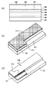
(第1の実施の形態)
図1は、本実施形態における2波長半導体レーザ1の斜視図である。また、図2は、図1に示した2波長半導体レーザ1を共振器方向に対して垂直に切断したときの断面図である。
2波長半導体レーザ1は、互いに異なる波長のレーザ光を発振する少なくとも二つのレーザ構造体を含む半導体発光素子である。
2波長半導体レーザ1は、第一基板(n型GaN基板101)、n型GaN基板101の所定の面に配置される第二基板(n型GaAs基板201)、n型GaN基板101の一方の面に設けられるとともに、第一活性層(多重量子井戸活性層105)を含む第一レーザ構造体(青紫色レーザ100)、およびn型GaAs基板201の一方の面に設けられるとともに、第二活性層(多重量子井戸活性層205)を含む第二レーザ構造体(赤色レーザ200)を含む。共振器長の短いGaN系の青紫色レーザ100のチップつまりn型GaN基板101上に、共振器長の長いAlGaInP系の赤色レーザ200が集積されている。多重量子井戸活性層105および多重量子井戸活性層205は、n型GaN基板101に対して同じ側に設けられている。赤色レーザ200は、青紫色レーザ100の側方に配置されている。(First embodiment)
FIG. 1 is a perspective view of a two-
The two-
The two-
青紫色レーザ100と赤色レーザ200とは、共振器長の方向が略平行になるように配置されており、青紫色レーザ100の共振器長が、赤色レーザ200の共振器長よりも短い。
青紫色レーザ100の共振器長をL1、赤色レーザ200の共振器長をL2、n型GaN基板101の共振器長方向の長さをL0としたときに、L1<L2であるとともに、L0がL2と同等かまたはL2よりも大きく、赤色レーザ200の放熱性が充分に確保される程度にn型GaN基板101の長さが確保されている。また、2波長半導体レーザ1において、L0>L1である。
青紫色レーザ100の熱伝導率は、赤色レーザ200の熱伝導率よりも大きい。なお、レーザ構造体の熱伝導率とは、レーザ構造体において、基板上に形成された半導体層の熱伝導率であり、たとえば両クラッド層とそれにはさまれた活性層とから構成される積層体の熱伝導率である。The blue-
When the resonator length of the blue-
The thermal conductivity of the blue-
赤色レーザ200は、n型GaN基板101に所定の層を介して接合されている。たとえば、赤色レーザ200がn型GaN基板101上にたとえば熱融着により接着されている。赤色レーザ200はp側ダウンの形態で青紫色レーザ100のp側に融着されている。赤色レーザ200を構成する層の中で最も熱抵抗の高いp型クラッド層207(p型(Al0.7Ga0.3)0.47In0.53P層)の側をn型GaN基板101に対向させることにより、赤色レーザ200の放熱性をさらに高めることができる。赤色レーザ200においては、p型クラッド層207の熱抵抗が高く、p型クラッド層207の全面をn型GaN基板101の所定の面に所定の層を介して接着することにより、放熱特性が向上する。The
青紫色レーザ100の前端面および後端面のうち、ここでは後端面123がエッチングにより形成されている。また、多重量子井戸活性層105の一部をエッチング除去することにより、青紫色レーザ100の後端面123が、n型GaN基板101の端面よりもn型GaN基板101の内側に後退して形成されているとともに、赤色レーザ200の後端面223よりもn型GaN基板101の内側に後退して形成されている。
一方、レーザの前端面については、青紫色レーザ100の前端面124と、赤色レーザ200の前端面224とが、いずれもn型GaN基板101の同一の端面に一致する。Of the front end face and the rear end face of the blue-
On the other hand, regarding the front end face of the laser, the
また、青紫色レーザ100の平面形状は矩形であって、青紫色レーザ100の一方の面において、多重量子井戸活性層105の一部がエッチングにより除去された領域を有する。多重量子井戸活性層105の平面形状は略L字型である。赤色レーザ200は、多重量子井戸活性層105が除去されていない領域において、n型GaN基板101の当該一方の面に配置されている。こうすれば、n型GaN基板101の上部の多重量子井戸活性層105が除去された領域を放熱領域として機能させることができるため、素子全体の放熱特性を向上させることができる。また、青紫色レーザ100の後端面123が、多重量子井戸活性層105が欠損した領域の外周縁により規定されているため、青紫色レーザ100の種類に応じて青紫色レーザ100の共振器長を所定の長さに設定可能な構成となっている。
Further, the planar shape of the blue-
青紫色レーザ100は、リッジ型の上部クラッド(p型クラッド層108)を含むGaN系レーザである。青紫色レーザ100のチップ、ここではn型GaN基板101の大きさは、たとえば幅400μm、長さ1600μmである。なお、本実施の形態および以下の実施の形態において、チップの幅は、導波路方向(共振器長方向)に対する断面方向の基板の長さを指し、チップの長さは、導波路方向に平行な方向の基板の長さを指す。
また、青紫色レーザ100においては、共振器長が600μmになるように後端面をエッチングで形成し、不必要な発光層を除去してある。青紫色レーザ100においては、光が出射する前端面124に、反射率が10%の低反射コーティング(不図示)が施されている。また、青紫色レーザ100の後端面123には、反射率が90%の高反射コーティング(不図示)が施されている。
この青紫色レーザ100は、CWでたとえば200mW以上の光出力が可能な構造である。The blue-
In the blue-
This blue-
また、赤色レーザ200は、リッジ型の上部クラッド(p型クラッド層207)を含むAlGaInP系のレーザである。赤色レーザ200のチップ、ここではn型GaAs基板201の大きさは、たとえば幅250μm、長さ1500μmである。
赤色レーザ200においては、光が出射する前端面224には、7%の低反射コーティングが施されている。また、赤色レーザ200の後端面223には、95%の高反射コーティングが施されている。
この赤色レーザ200はパルス動作(たとえばパルス幅30ns、デューティー比30%)でたとえば240mW以上の光出力が可能な構造である。The
In the
The
以下、図2を参照して、青紫色レーザ100および赤色レーザ200の構成をさらに詳細に説明する。
Hereinafter, the configurations of the blue-
青紫色レーザ100においては、n型GaN基板101(たとえば、厚さ約100μm、n=3×1018cm-3)上に、n型バッファ層102(たとえば、n型GaN層、厚さ1μm、n=1×1018cm-3)、n型クラッド層103(たとえば、n型Al0.07Ga0.93N層、厚さ1.3μm、n=7×1017cm-3)、n側光閉じ込め層104(たとえば、n型GaN層、厚さ50nm、n=5×1017cm-3)、In0.1Ga0.9Nウェル(たとえば、厚さ3.5nm)とIn0.02Ga0.98Nバリア(たとえば、厚さ8.5nm)からなる多重量子井戸活性層105、p側光閉じ込め層106(たとえば、GaN層、厚さ80nm)、オーバーフロー防止層として機能するp型電子障壁層107(たとえば、p型Al0.16Ga0.84N層、厚さ10nm、p=5×1017cm-3)、p型クラッド層108(たとえば、p型AlGaN層、厚さ500nm、p=7×1017cm-3)およびp型コンタクト層109(たとえば、p型GaN層、厚さ100nm、p=1×1018cm-3)が積層されている。
なお、本明細書において、「n=」および「p=」とは、それぞれ、層中のn型キャリア(電子)の濃度およびp型キャリア(正孔)の濃度を示す。In the blue-violet laser 100, an n-type buffer layer 102 (for example, an n-type GaN layer, a thickness of 1 μm, on an n-type GaN substrate 101 (for example, a thickness of about 100 μm, n = 3 × 10 18 cm −3 ), n = 1 × 10 18 cm −3 ), n-type cladding layer 103 (for example, n-type Al 0.07 Ga 0.93 N layer, thickness 1.3 μm, n = 7 × 10 17 cm −3 ), n-side optical confinement layer 104 (eg, n-type GaN layer, thickness 50 nm, n = 5 × 10 17 cm −3 ), In 0.1 Ga 0.9 N well (eg, thickness 3.5 nm) and In 0.02 Ga 0.98 N barrier (eg, thickness) 8.5 nm), a multi-quantum well active layer 105, a p-side optical confinement layer 106 (for example, GaN layer, thickness 80 nm), and a p-type electron barrier layer 107 (for example, p-type Al 0.16 functioning as an overflow prevention layer) Ga 0.84 N layer, Is 10nm, p = 5 × 10 17 cm -3), p -type cladding layer 108 (e.g., p-type AlGaN layer, the thickness of 500nm, p = 7 × 10 17 cm -3) and p-type contact layer 109 (e.g., A p-type GaN layer, a thickness of 100 nm, and p = 1 × 10 18 cm −3 ) are stacked.
In this specification, “n =” and “p =” indicate the concentration of n-type carriers (electrons) and the concentration of p-type carriers (holes) in the layer, respectively.
また、横モード制御のために、p型クラッド層108の厚さ方向に途中までエッチングされ、リッジ121が形成されている。p型コンタクト層109は、リッジ121の頂部すなわちp型クラッド層108の上面に設けられている。さらに、リッジ121の外側には、p型クラッド層108の側面から底面を被覆する酸化シリコン膜110が積層されている。
Further, in order to control the transverse mode, the
また、p型コンタクト層109には、コンタクト層側から順にパラジウム/白金/金(Pd/Pt/Au)で構成されるp側電極111が設けられている。また、n型GaN基板101の裏面には、基板側から順にチタン/白金/金(Ti/Pt/Au)で構成されるn側電極112が形成されている。
The p-
一方、赤色レーザ200においては、n型GaAs基板201(たとえば、厚さ約120μm、n=2×1018cm-3)上に、n型バッファ層202(たとえば、n型GaAs層、厚さ500nm、n=1×1018cm-3)、n型クラッド層203(たとえば、n型(Al0.7Ga0.3)0.47In0.53P層、厚さ2μm、n=8×1017cm-3)、n側光閉じ込め層204(たとえば、(Al0.5Ga0.5)0.47In0.53P層、厚さ30nm)、GaInPウェルとAlGaInPバリアからなる多重量子井戸活性層205、p側光閉じ込め層206(たとえば、(Al0.5Ga0.5)0.47In0.53P層、厚さ30nm)、p型クラッド層207(たとえば、p型(Al0.7Ga0.3)0.47In0.53P層、厚さ1.5μm、p=8×1017cm-3)およびp型コンタクト層208(たとえば、p型GaAs層、厚さ400nm、p=5×1018cm-3)が積層されている。On the other hand, in the
また、赤色レーザ200においては、横モード制御のために、p型クラッド層207が厚さ方向に途中までエッチングされ、リッジ221が形成されている。p型コンタクト層208は、リッジ221の頂部すなわちp型クラッド層207の下面に設けられている。さらに、リッジ221の外側には、p型クラッド層207の側面から上面を被覆する酸化シリコン膜209が積層されている。
In the
また、p型コンタクト層208には、コンタクト層側から順にTi/Pt/Auで構成されるp側電極210が設けられている。また、n型GaAs基板201の裏面には、基板側から順に金・ゲルマニウム/ニッケル/金(AuGe/Ni/Au)で構成されるn側電極211が形成されている。
The p-
赤色レーザ200は、p側ダウンの形態で、青紫色レーザ100上に金(Au)とすず(Sn)からなる融着材113を介して融着されている。なお、青紫色レーザ100と赤色レーザ200との発光点間隔は、できるだけ近い方が光ピックアップの光軸調整に有利である。従って、各々のレーザのチップの中におけるリッジの形成位置を調整して、発光点ができるだけ近づくようにするとよい。
The
次に、2波長半導体レーザ1の製造方法について説明する。図3〜図6は、それぞれ、2波長半導体レーザ1の製造方法を示す図である。図3(a)〜図3(c)、図4(a)および図4(b)は、GaN系の青紫色レーザ100の製造工程を示す図であり、図5(a)、図5(b)、図6(a)および図6(b)は、AlGaInP系の赤色レーザ200の製造工程を示す断面図である。
Next, a method for manufacturing the two-
まず、図3(a)〜図3(c)、図4(a)および図4(b)を参照して、GaN系の青紫色レーザ100の製造工程について説明する。この製造工程では、後端面123をドライエッチングで形成する一方、光を取り出す前端面124をへき開で形成する。
First, the manufacturing process of the GaN-based blue-
はじめに、たとえば厚さ400μm程度のn型GaN基板101上に、n型バッファ層102、n型クラッド層103、n側光閉じ込め層104、多重量子井戸活性層105、光閉じ込め層106すなわちノンドープp側GaN層、p型AlGaN電子障壁層107、p型クラッド層108およびp型コンタクト層109を順次結晶成長させる(図3(a))。なお、図3(b)および図3(c)では、これらの成長層のうち、一部の層の図示を省略する。
First, for example, an n-
結晶成長には、たとえば有機金属気相成長(MOVPE)法を用い、原料として、たとえばトリメチルアルミニウム(TMAl)、トリメチルガリウム(TMGa)、トリエチルガリウム(TEGa)、トリメチルインジウム(TMIn)およびアンモニア(NH3)を用いる。また、n型およびp型のドーパントには、それぞれ、たとえばシリコン(Si)およびマグネシウム(Mg)を用い、これらの原料として、それぞれ、たとえばシラン(SiH4)およびシクロペンタジエチルマグネシウム(Cp2Mg)を用いる。また、キャリアガスには各成長層の組成に応じて水素または窒素を用いる。For example, metal organic vapor phase epitaxy (MOVPE) is used for crystal growth, and as raw materials, for example, trimethylaluminum (TMAl), trimethylgallium (TMGa), triethylgallium (TEGa), trimethylindium (TMIn), and ammonia (NH 3 ). ) Is used. Further, for example, silicon (Si) and magnesium (Mg) are used for the n-type and p-type dopants, respectively. For example, silane (SiH 4 ) and cyclopentadiethyl magnesium (Cp 2 Mg) are used as these raw materials. Is used. As the carrier gas, hydrogen or nitrogen is used depending on the composition of each growth layer.
次に、ドライエッチングにより、青紫色レーザ100の後端面123を形成する。まず、熱化学気相堆積(熱CVD)法、プラズマCVD法、スパッタ法または電子ビーム蒸着法等の方法を用いて、酸化シリコン膜114を堆積し、ステッパーや密着露光などのフォトリソグラフィーを用いて、酸化シリコン膜114の所定の領域を選択的にエッチング除去する。エッチング後の酸化シリコン膜114の平面形状は、たとえばL字型とする。そして、酸化シリコン膜114をマスクとして、ドライエッチングにより、n型GaN基板101に達するまで成長層を除去し、成長層長を短くする(図3(b))。なお、図3(b)に示すように、エッチングされた側面は、青紫色レーザ100の後端面123となるので、できるだけ平滑にかつ基板面内方向に対して垂直になるようにエッチングすることが望ましい。
Next, the
つづいて、リッジ121を形成する。まず、p型コンタクト層109に、たとえば幅1.5μmのストライプ状の酸化シリコン膜115を形成する。酸化シリコン膜115は、図3(b)を参照して前述した工程により成長層が短くなっている領域に、共振器長方向に延在するように形成される。また、酸化シリコン膜115は、酸化シリコン膜114を除去後、再度、別の酸化シリコン膜を堆積し、これをフォトリソグラフィーにより所定の領域のみ選択的に残存させることにより形成される。または、別の酸化シリコン膜を設ける方法に代えて、図3(b)に示した工程の後、酸化シリコン膜114をさらにフォトリソグラフィーを用いて所定の形状に加工して形成してもよい。
Subsequently, the
そして、酸化シリコン膜115をマスクとして、ドライエッチングにより、p型コンタクト層109およびp型クラッド層108の一部をエッチングし、リッジ121を形成する(図3(c))。
Then, using the
ついで、p側電極111を形成する。まず、ストライプ状の酸化シリコン膜115を除去後、n型GaN基板101の表面全面に、再度、別の酸化シリコン膜110を堆積する。次に、リッジトップの酸化シリコン膜110をエッチングにより除去し、p型コンタクト層109を露出させる。そして、p型コンタクト層109上に、p側電極111を構成する金属膜を堆積する(図4(a))。
Next, the p-
そして、へき開を容易にするために、n型GaN基板101を研磨し、たとえば100μm程度に薄化する。そして、研磨した面をクリーニング処理した後、研磨面に接しこれを被覆するn側電極112を形成する(図4(b))。次に、端面コーティングのために、ウェハをリッジ121が横に並んだバー状態となるようにへき開する。このとき、ドライエッチングで形成した後端面123の位置から600μmの位置でへき開し、前端面124とする。これにより、GaN系の青紫色レーザ100の共振器長が600μmとなる。
In order to facilitate cleavage, the n-
また、チップの長さすなわちn型GaN基板101の共振器長方向の長さが1600μmとなるように、反対側をへき開する。そして、前端面124には反射率10%の低反射コーティングを施し、後端面123には90%の高反射コーティングを施す。コーティング材のうち、低屈折率の材料としては、たとえば、アルミナや酸化シリコン、窒化アルミニウム、フッ化マグネシウム、またはフッ化カルシウムを用いる。また、コーティング材のうち、高屈折率の材料としては、たとえば、酸化チタンや酸化ジルコニウム、酸化ハーフニウムなどを用いる。最後に、複数のリッジ121がバー状態に平行に並んだウェハを複数のチップに個片化するへき開を行う。以上の手順により、青紫色レーザ100が得られる。
Further, the opposite side is cleaved so that the length of the chip, that is, the length of the n-
次に、図5(a)、図5(b)、図6(a)および図6(b)を参照して、AlGaInP系の赤色レーザ200の製造工程を説明する。
はじめに、たとえば厚さ350μm程度のn型GaAs基板201上に、n型GaAs202、n型クラッド層203、n側光閉じ込め層204(たとえばAlGaInP層)、多重量子井戸活性層205、p側光閉じ込め層206(たとえばAlGaInP層)、p型クラッド層207およびp型コンタクト層208を順次結晶成長させる(図5(a))。Next, a manufacturing process of the AlGaInP
First, an n-
結晶成長には、たとえばMOVPE法を用い、原料として、たとえばTMAl、TEGa、TMIn、アルシン(AsH3)およびホスフィン(PH3)を用いる。また、n型およびp型のドーパントには、それぞれ、たとえばSiおよび亜鉛(Zn)を用い、これらの原料として、それぞれ、たとえばジシラン(Si2H6)およびジエチル亜鉛(DEZn)を用いる。また、キャリアガスには、たとえば水素を用いる。For example, MOVPE is used for crystal growth, and TMAl, TEGa, TMIn, arsine (AsH 3 ), and phosphine (PH 3 ) are used as raw materials. Further, for example, Si and zinc (Zn) are used for n-type and p-type dopants, respectively, and for example, disilane (Si 2 H 6 ) and diethyl zinc (DEZn) are used as these raw materials. Further, for example, hydrogen is used as the carrier gas.
次に、リッジ221を形成する。まず、熱CVD法またはプラズマCVD法またはスパッタ法または電子ビーム蒸着法等を用いて、酸化シリコン膜212を堆積する。そして、ステッパーや密着露光などのフォトリソグラフィーを用いて酸化シリコン膜212の所定の領域を選択的に除去することにより、共振器長方向に延在する幅1.5μmのストライプ形状に酸化シリコン膜212を加工する。そして、ドライエッチング等により、酸化シリコン膜212をマスクとして、p型コンタクト層208およびp型クラッド層207の一部を選択的にエッチング除去し、リッジ221を形成する(図5(b))。
Next, the
次に、p側電極210を形成する。まず、ストライプ状の酸化シリコン膜212を除去した後、再度、別の酸化シリコン膜209を堆積する。次に、リッジトップの酸化シリコン膜209をエッチングにより選択的に除去し、p型コンタクト層208を露出させる。そして、p型コンタクト層208上に、p側電極210を構成する各金属膜を堆積する(図6(a))。
Next, the p-
そして、へき開を容易にするために、n型GaAs基板201を研磨によりたとえば120μm程度に薄化する。そして、研磨した面をクリーニング処理した後、研磨面に接しこれを被覆するn側電極211を形成する(図6(b))。次に、端面コーティングのために共振器長が1500μmになるようにへき開を行う。そして、前端面224には反射率7%の低反射コーティングを、後端面223には95%の高反射コーティングを施す。最後に、複数のリッジ221がバー状態に並んだウェハを複数のチップに個片化するへき開を行う。以上の手順により、赤色レーザ200が得られる。
In order to facilitate cleavage, the n-
なお、赤色レーザ200では、端面劣化を防止するために窓構造と電流非注入構造が採用されている。
The
こうして得られた赤色レーザ200は、図2に示すように融着材113を用いてp側ダウンの形態で青紫色レーザ100のp側に融着される。以上により、図1に示した2波長半導体レーザ1が得られる。
The
次に、2波長半導体レーザ1を含むパッケージについて説明する。図7は、本実施の形態に示した2波長半導体レーザ1を直径5.6mmのパッケージに組み込んだ状態を示す斜視図である。
Next, a package including the two-
パッケージの本体10の材料は、たとえば鉄とし、支持体11ならびにフィードスルー12、13および14の材料は、たとえば銅とする。また、本体10、支持体11および各フィードスルーは表面が金でコーティングされている。
The material of the
また、フィードスルー12およびフィードスルー13は、セラミック等の絶縁体15を介して本体10に取り付けられている。こうすることにより、これらのフィードスルーと本体10との絶縁性が確保される。また、フィードスルー14は、本体10に接続され、支持体11と電気的に接続されている。
The
2波長半導体レーザ1は、青紫色レーザ100のn側電極112の面において、融着材16を介して支持体11に融着されている。融着材16としては、たとえば、低融点の金・すずや鉛・すずなどが用いられる。さらに、フィードスルー12と青紫色レーザ100のp側電極111とが、またフィードスルー13と赤色レーザ200のn側電極211とが、それぞれ、金のワイヤー17でボンディングされている。
The two-
本実施の形態の2波長半導体レーザ1において、フィードスルー12にプラス電圧を印加し、フィードスルー14にマイナス電圧を印加することにより、青紫色レーザ100がレーザ発振する。また、フィードスルー12にプラス電圧を印加し、フィードスルー13にマイナス電圧を印加することにより、赤色レーザ200がレーザ発振する。
In the two-
青紫色レーザ100と赤色レーザ200とを集積した2波長半導体レーザ1では、ヒートシンクの役割をなすGaN系の青紫色レーザ100のチップの長さが、これに融着されるAlGaInP系の赤色レーザ200のチップと同等かまたは長くなっている。このため、赤色レーザ200のチップで発生した熱は青紫色レーザ100を介して支持体11から効率よく放熱される。よって、共振器長が1500μmと長い赤色レーザ200の放熱性が確保され、高出力特性を実現することができる。
In the two-
ここで、背景技術の項で前述した特許文献1においては、波長650nmの半導体発光体素子の基板に、波長780nmの半導体発光素子の基板を貼り合わせた構成において、これらの半導体発光素子の前端面の位置をそろえて、後端面をオフセットすることにより、ボンディング領域を確保している。ところが、この構成の場合、各半導体発光素子の共振器長がいずれも基板の長さと等しく、基板の厚さに依存して決まる構成となっている。このため、本実施の形態の場合のように、面積の大きい基板にGaN系の青紫色レーザ等を用いようとした場合にも、その共振器長が長くなってしまう。このため、青紫色レーザのレーザ特性および信頼性が充分に確保されない懸念があった。
Here, in
これに対し、本実施の形態においては、青紫色レーザ100においては、チップの長さが1600μmと長いが、共振器長が600μmとなるように後端面123がドライエッチングにより形成されている。ドライエッチングなどで後端面123を形成し、レーザ発振に必要な共振器長をチップの長さより短くすることにより、導波路損失の低減や、n型GaN基板101から導波路ストライプへ伝播する転位の数が低減し、高効率・低動作電流でのレーザ発振と高信頼性を実現することができる。このため、600μm共振器長の通常のGaN系青紫色レーザと同等のレーザ特性と信頼性を実現できる。
On the other hand, in the present embodiment, in the blue-
以上のように、2波長半導体レーザ1によれば、熱伝導性と共振器長のバランスを確保し、レーザ特性と信頼性に優れた集積レーザが実現される。
As described above, according to the two-
また、本実施の形態においては、青紫色レーザ100の後端面123が、エッチングにより形成されるため、後端面123を制御性よく形成し、製造時の青紫色レーザ100の共振器長のばらつきを好適に抑制することができる。
In the present embodiment, since the
なお、技術分野は異なるが、特許文献2には、モノリシックに形成された二つのレーザのエッチドミラー面を、同一のエッチング工程により形成し、ミラー面の位置を共振器長方向に異ならせる技術が記載されている。この場合、同一のエッチング工程によりエッチング可能な材料で二つのレーザが構成されている必要がある。
Although the technical fields are different,
これに対し、本実施の形態においては、それぞれの半導体レーザを別個の基板上に形成した後、一方を他方の基板と接合する。このため、それぞれの半導体レーザの特性に応じて、端面の位置および共振器長をさらに高い自由度で設計し、安定的に製造することができる。そして、GaN系の青紫色レーザ100に、多重量子井戸活性層105の形成領域とこれが除去された欠損領域が設けられており、赤色レーザ200が多重量子井戸活性層105の形成領域に配置されている。このため、青紫色レーザ100および赤色レーザ200の放熱領域として欠損領域を効果的に利用することができる。
On the other hand, in this embodiment, after forming each semiconductor laser on a separate substrate, one is bonded to the other substrate. Therefore, according to the characteristics of each semiconductor laser, the position of the end face and the resonator length can be designed with a higher degree of freedom and can be manufactured stably. The GaN-based blue-
また、2波長半導体レーザ1においては、青紫色レーザ100の前端面124と赤色レーザ200の前端面224とが、いずれもn型GaN基板101の端面に一致し、これらの端面が同一直線上に配置されている。このため、青紫色レーザ100からの出射光の焦点と赤色レーザ200からの出射光との焦点が同一平面内に位置する構成となっている。このため、受光系の装置構成を簡素化することができる。
In the two-
なお、本実施の形態では、GaN系の青紫色レーザ100とAlGaInP系の赤色レーザ200を集積した場合を例に説明した。n型GaN基板101上に集積されるレーザ構造体は、AlGaInP系には限られず、たとえば、AlGaAs系、GaInAs系、AlGaInAs系、InGaAsP系、InGaAsN系またはInGaAsNSb系のレーザとしてもよい。
In the present embodiment, the case where the GaN blue-
さらに具体的には、AlGaInP系の赤色レーザ200の代わりにAlGaAs系の赤外レーザを集積した2波長半導体レーザとしてもよい。この場合、AlGaAsはAlGaInPに比べて熱伝導率が高いため、たとえば共振器長が900μmとAlGaInP系の場合よりも短い構成においても、たとえばパルス動作(パルス幅50ns、デューティー比50%)200mWが可能である。従って、GaN系の青紫色レーザ100のチップ、つまりn型GaN基板101の共振器長方向の長さを900μm以上と短くすることができる。この場合にも、n型GaN基板101上にAlGaAs系赤外レーザを集積し、放熱性を充分に確保することができる。
More specifically, instead of the AlGaInP
また、本実施の形態では、GaN系の青紫色レーザ100の導波路方向(共振器長方向)のチップの長さが1600μmで、チップ上に融着するAlGaInP系の赤色レーザ200のチップの長さより長い2波長半導体レーザ1の場合を例に説明した。さらに具体的には、赤色レーザ200のチップの長さが導波路の長さおよび共振器長に等しく、1500μmである場合を例示した。
In the present embodiment, the length of the chip in the waveguide direction (resonator length direction) of the GaN-based blue-
しかし、赤色レーザ200の放熱性が充分に確保できる形態であれば、L0がL2よりも大きい構成には限られず、L2と同等である構成とすることも可能であり、厳密なチップの長さの大小関係は逆(L0<L2)の構成を採用してもよい。放熱性をさらに確実に得る観点では、たとえば、n型GaN基板101の共振器長方向の長さをn型GaAs基板201の共振器長方向の長さの90%以上、好ましくは95%以上とすることができる。さらに具体的には、n型GaN基板101の長さを1500μmとし、n型GaAs基板201の長さを1520μmとしてもよい。この場合、青紫色レーザ100のチップ上に、赤色レーザ200を集積したときに、赤色レーザ200の前端面側10μmと後端面側10μmとが青紫色レーザ100のチップからはみ出すことになる。こうした構成においても、赤色レーザ200の基板201の大部分が青紫色レーザ100に接しており、実用上問題ない程度の充分な放熱性が確保される。このような場合も、チップの長さは同等と考えることができる。
However, as long as the heat dissipation of the
また、赤色レーザ200の後端面223の位置と、n型GaN基板101の端面の位置とが一致するとともに、青紫色レーザ100の前端面124および赤色レーザ200の前端面124がいずれもn型GaN基板101の同一の端面に一致していてもよい。これは、L0=L2となる構成である。このようにすれば、赤色レーザ200の放熱特性を充分に確保しつつ、2波長半導体レーザ1全体の小型化が可能である。
Further, the position of the
以下、第1の実施の形態と異なる点を中心に説明する。
(第2の実施の形態)
図8は、本実施の形態の2波長半導体レーザの構成を示す斜視図である。この2波長半導体レーザの基本構成は、第1の実施の形態における2波長半導体レーザ1と同様であるが、青紫色レーザ100の後端面123をドライエッチングで作製する時に、後端面123に対向する面を後端面に対して45゜に傾斜した反射ミラー116が形成された点が異なる。The following description will focus on differences from the first embodiment.
(Second Embodiment)
FIG. 8 is a perspective view showing the configuration of the two-wavelength semiconductor laser of the present embodiment. The basic configuration of this two-wavelength semiconductor laser is the same as that of the two-
図8においては、n型GaN基板101の一方の面において、多重量子井戸活性層105の除去された領域に反射ミラー116を設けて、多重量子井戸活性層105の除去された領域を有効活用することができる。青紫色レーザ100の後端面123から出射された光を反射ミラー116にて反射させてチップの側方に取りだし、受光素子(不図示)で受光する構成とし、レーザ動作のモニター光として利用することができる。
In FIG. 8, on one surface of the n-
(第3の実施の形態)
図9は、本実施の形態の2波長半導体レーザ3の構成を示す斜視図である。この2波長半導体レーザの基本構成は、第1の実施の形態における2波長半導体レーザ1と同様であり、GaN系の青紫色レーザ100のチップ上にAlGaInP系の赤色レーザ200が集積されている。第1の実施の形態との違いは、青紫色レーザ100のn側電極112が、n型GaN基板101の裏面ではなく、後端面123を作製するためにエッチングした領域のn型GaN基板101上に形成されていることである。(Third embodiment)
FIG. 9 is a perspective view showing the configuration of the two-
このような構成とすることにより、p側電極111とn側電極112に同じ電極材料(たとえば、Ti/Pt/Auなど)を用いて、p側電極111とn側電極112とを同時に形成することができる。その結果、電極形成のプロセス工程を減らすことができる。また、n型GaN基板101の一方の面において、多重量子井戸活性層105の除去された領域を有効活用することができる。
With this configuration, the p-
また、p側電極111とn側電極112の材料が異なる場合にも、作製順序を任意に選ぶことができる。その結果、それぞれの電極について、アロイ条件などコンタクト抵抗が最小になる最適プロセスが適用できるという利点がある。なお、図3を参照して前述したプロセスでは、リッジ側の電極形成(図3の場合、p側電極111)が先に行われる。こうすれば、酸化シリコン膜110の堆積、パターニングなどのプロセスが必要なリッジ側の電極形成を基板研磨前の状態で行うことができるため、製造安定性を向上させることができる。
In addition, even when the materials of the p-
また、本実施の形態においては、青紫色レーザ100をパッケージに組み込む際に、支持体11を電気的に分離するか、または、窒化アルミニウムのヒートシンク等の半絶縁性のサブマウントを介して青紫色レーザ100を支持体11に融着することにより、青紫色レーザ100を電気的にフローティング状態にすることができるという利点もある。
Further, in the present embodiment, when the blue-
(第4の実施の形態)
図10は、本実施の形態の2波長半導体レーザの構成を示す斜視図である。この2波長半導体レーザの基本構成は、第1の実施の形態における2波長半導体レーザ1と同様であり、GaN系の青紫色レーザ100のチップ上にAlGaInP系の赤色レーザ200がp側ダウンの形態で融着材を介して集積されている。図10においては、青紫色レーザ100の前端面124と後端面123とが、いずれもドライエッチングにより形成された面である点が、第1の実施の形態と異なる。また、前端面124が前端面224よりもn型GaN基板101の内側に後退している。(Fourth embodiment)
FIG. 10 is a perspective view showing the configuration of the two-wavelength semiconductor laser of the present embodiment. The basic configuration of this two-wavelength semiconductor laser is the same as that of the two-
この構成によれば、共振器長がエッチングプロセスで決定されるため、ウェハからチップにへき開する際に、厳密な共振器長の制御をする必要がない。また、青紫色レーザ100のGaN基板は非常に硬いために、研磨後のウェハ厚が不均一であったりへき開の条件が悪かったりする場合、へき開面に傷(段差)が形成される懸念がある。これに対し、本実施の形態においては、そのような懸念がなく、エッチングにより青紫色レーザ100の共振器長の制御性をさらに向上させることができる。
According to this configuration, since the resonator length is determined by the etching process, it is not necessary to strictly control the resonator length when cleaving from the wafer to the chip. Further, since the GaN substrate of the blue-
また、n型GaN基板101の後端面123の側と前端面124の両方に多重量子井戸活性層105の除去された領域が設けられているため、2波長半導体レーザ1内における放熱されやすさのばらつきを抑制することができる。
In addition, since the region where the multiple quantum well
(第5の実施の形態)
図11は、本実施の形態の2波長半導体レーザの構成を示す斜視図である。図12は、図11の2波長半導体レーザに用いた青紫色レーザ100の構成を示す斜視図である。(Fifth embodiment)
FIG. 11 is a perspective view showing the configuration of the two-wavelength semiconductor laser according to the present embodiment. FIG. 12 is a perspective view showing the configuration of the blue-
この2波長半導体レーザの基本構成は、第1の実施の形態における2波長半導体レーザ1と同様であり、GaN系の青紫色レーザ100のチップ上にAlGaInP系の赤色レーザ200がp側ダウンの形態で融着材113を介して集積されている。図11においては、青紫色レーザ100のリッジ導波路(図12のリッジ121)の直上に赤色レーザ200が融着されている点が第1の実施の形態と異なる。
The basic configuration of this two-wavelength semiconductor laser is the same as that of the two-
また、図12に示したように、多重量子井戸活性層105が基板面内の中央付近の領域において欠損しており、その平面形状が略「ロ」の字型である。n型GaN基板101の一方の面において、青紫色レーザ100の後端面123およびその近傍の多重量子井戸活性層105が除去されている。多重量子井戸活性層105は、青紫色レーザ100の後端面123から共振器長方向後方、つまり共振器長方向に青紫色レーザ100から遠ざかる方向に除去されている。
Further, as shown in FIG. 12, the multi-quantum well
リッジ121の直上に赤色レーザ200を融着することにより、青紫色レーザ100と赤色レーザ200との発光点間隔が近くなる。このため、光ピックアップの光軸調整の点で非常に有利な構成である。
By fusing the
図12においても、青紫色レーザ100の共振器長を600μmとするために、第1の実施の形態で前述した方法を用いて後端面123をエッチングにより形成する。しかし、図12においては、エッチングする領域を幅約20μm、長さ約10μmと第1の実施の形態の場合よりも狭い領域にする。これにより、直上に融着する赤色レーザ200の放熱性を確保することができる。よって、より一層優れた出力特性を得ることができる。
Also in FIG. 12, in order to set the resonator length of the blue-
(第6の実施の形態)
図13は、本実施の形態の2波長半導体レーザの構成を示す斜視図である。この2波長半導体レーザの基本構成は、第1の実施の形態における2波長半導体レーザ1と同様であり、青紫色レーザ100のチップ上に赤色レーザ200がp側ダウンの形態で融着材を介して融着されている。青紫色レーザ100と赤色レーザ200の構造は、第4の実施の形態に用いた構造とする。第4の実施の形態との違いは、多重量子井戸活性層105と多重量子井戸活性層205とが、n型GaN基板101に対して異なる側に設けられた点である。具体的には、赤色レーザ200が青紫色レーザ100の基板裏面側に融着されている。(Sixth embodiment)
FIG. 13 is a perspective view showing the configuration of the two-wavelength semiconductor laser of the present embodiment. The basic configuration of the two-wavelength semiconductor laser is the same as that of the two-
n型GaN基板101の裏面は平坦であるため、この裏面に赤色レーザ200を融着すれば、赤色レーザ200のリッジに大きな歪を与えることなく、チップ全体を青紫色レーザ100に融着することが可能である。従って、組み立て時の歩留まり低下を抑制することができる。
Since the back surface of the n-
また、本実施の形態の2波長半導体レーザをパッケージに組み込む場合、青紫色レーザ100のp側ダウンの形態で、たとえば図5に示した直径5.6mmのパッケージに組み込まれる。その場合、支持体11に、直接またはサブマウントを介して融着される。従って、第4の実施の形態の場合に比べて、青紫色レーザ100の放熱性が向上し、高出力特性や温度特性が向上するという利点がある。
Further, when the two-wavelength semiconductor laser of the present embodiment is incorporated into a package, it is incorporated into a package with a diameter of 5.6 mm shown in FIG. In that case, it fuse | fuses to the
以上の実施の形態では、2波長半導体レーザの場合を例に説明したが、本発明の実施の形態は2波長半導体レーザの場合に限られず、青紫色レーザ100のチップ、ここではn型GaN基板101上に、第2、第3、第(n+1)のn個の半導体レーザ(n=1、2、3、・・・)を接着した集積型半導体レーザとすることができる。このとき、集積する第(n+1)の半導体レーザの共振器長をL(n+1)とすると、L0がL(n+1)と同等かより大きい構成とすることができる。
以下、3波長半導体レーザの実施の形態を説明する。In the above embodiment, the case of the two-wavelength semiconductor laser has been described as an example. However, the embodiment of the present invention is not limited to the case of the two-wavelength semiconductor laser, and the chip of the blue-
Hereinafter, embodiments of the three-wavelength semiconductor laser will be described.
(第7の実施の形態)
図14は、本実施の形態の3波長半導体レーザ2の構成を示す斜視図である。図15は、図14に示した3波長半導体レーザ2の断面図である。また、図16は、図15の3波長半導体レーザ2の青紫色レーザ100の斜視図である。(Seventh embodiment)
FIG. 14 is a perspective view showing the configuration of the three-
3波長半導体レーザ2は、第三半導体基板(n型GaAs基板301)の一方の面に設けられた第三活性層(多重量子井戸活性層305)を含み、共振器長がL3の第三レーザ構造体(赤外レーザ300)をさらに含む。赤色レーザ200および赤外レーザ300は、n型GaN基板101に対して同じ側に設けられている。具体的には、GaN系の青紫色レーザ100のチップ上に、AlGaInP系の赤色レーザ200とAlGaAs系の赤外レーザ300とが集積されている。赤色レーザ200および赤外レーザ300は、いずれもp側ダウンの形態で青紫色レーザ100のp側に融着されている。赤色レーザ200、青紫色レーザ100および赤外レーザ300が、共振器長方向が互いに平行になるようにこの順に並置されている。
The three-
青紫色レーザ100のチップの大きさは、たとえば幅400μm、長さ1600μmである。青紫色レーザ100においては、共振器長が600μmになるように後端面123がエッチングにより形成されている(図16)。また、エッチングにより、不必要な発光層が除去されている。多重量子井戸活性層105の平面形状は略「コ」の字型である。また、青紫色レーザ100において、光が出射する前端面124には反射率が10%の低反射コーティングが施されており、後端面123(図16中に図示)には90%の高反射コーティングが施されている。
The chip size of the blue-
図15に示したように、青紫色レーザ100の積層構造は、第1の実施の形態で示した青紫色レーザ100(図2)と同様である。しかし、図15においては、図2の場合と異なり、青紫色レーザ100のリッジ構造(リッジ121)がチップのほぼ中央に形成されている。これにより、赤色レーザ200の発光点と赤外レーザ300の発光点が、青紫色レーザ100の発光点を中心に左右対称になるように配置される。
As shown in FIG. 15, the laminated structure of the blue-
赤色レーザ200の構造は、第1の実施の形態で示した素子と同様であり、そのチップの大きさは、たとえば幅150μm、長さ1500μmである。また、赤色レーザ200において、光が出射する前端面224には7%の低反射コーティングが施されており、後端面223には95%の高反射コーティングが施されている。
The structure of the
赤外レーザ300のチップの大きさは、たとえば幅150μm、長さ900μmである。また、赤外レーザ300において、光が出射する前端面324には5%の低反射コーティングが施されており、後端面323には95%の高反射コーティングが施されている。
The size of the chip of the
また、図15に示したように、赤外レーザ300においては、n型GaAs基板301(たとえば厚さ120μm、n=2×1018cm-3)上に、n型バッファ層302(たとえば、n型GaAs層、厚さ1μm、n=1×1018cm-3)、n型クラッド層303(たとえば、n型Al0.5Ga0.5As層、厚さ2.2μm、n=7×1017cm-3)、n側光閉じ込め層304(たとえば、Al0.3Ga0.7As層、厚さ10nm)、AlGaAsウェルとAlGaAsバリアとからなる多重量子井戸活性層305、p側光閉じ込め層306(たとえば、Al0.3Ga0.7As層、厚さ10nm)、p型クラッド層307(たとえば、p型Al0.5Ga0.5As層、厚さ1.8μm、p=7×1017cm-3)およびp型コンタクト層308(たとえば、p型GaAs層、厚さ400nm、p=5×1018cm-3)が積層されている。As shown in FIG. 15, in the
また、赤外レーザ300において、横モード制御のために、p型コンタクト層308およびp型クラッド層307の一部が厚さ方向にエッチングにより除去され、リッジ321が形成されている。さらに、リッジ321はn型AlGaAs電流ブロック層309(たとえば厚さ1μm、n=7×1017cm-3)とn型GaAs電流ブロック層310(たとえば厚さ800nm、n=1×1018cm-3)で埋め込まれている。また、p型コンタクト層308上に、コンタクト層側から順にTi/Pt/Auで構成されるp側電極311が形成されている。また、n型GaAs基板301上に、AuGe/Ni/Auで構成されるn側電極312が形成されている。赤外レーザ300は赤色レーザ200と同様にp側ダウンの形態で青紫色レーザ100上にAuとSnからなる融着材113を介して融着されている。In the
次に、3波長半導体レーザ2の製造方法を説明する。青紫色レーザ100および赤色レーザ200は、第1の実施の形態で前述した方法を用いて得ることができる。
また、赤外レーザ300は、たとえば以下の手順で得られる。図17(a)〜図17(c)、図18(a)および図18(b)は、赤外レーザ300の製造工程を示す断面図である。Next, a method for manufacturing the three-
The
はじめに、n型GaAs基板301上に、n型バッファ層302、n型クラッド層303、n側光閉じ込め層304、多重量子井戸活性層305、p側光閉じ込め層306、p型クラッド層307およびp型コンタクト層308を順次結晶成長させる(図17(a))。
First, an n-
結晶成長には、たとえばMOVPE法を用い、原料として、たとえばTMAl、TMGa、TEGaおよびAsH3を用いる。また、n型およびp型のドーパントには、それぞれSiおよびZnを用いる。また、これらの原料として、それぞれ、たとえばSi2H6およびジメチル亜鉛(DMZn)を用いる。また、キャリアガスには、たとえば水素を用いる。For example, MOVPE is used for crystal growth, and TMAl, TMGa, TEGa, and AsH 3 are used as raw materials. Si and Zn are used for n-type and p-type dopants, respectively. Further, for example, Si 2 H 6 and dimethyl zinc (DMZn) are used as these raw materials, respectively. Further, for example, hydrogen is used as the carrier gas.
次に、リッジ321を形成する。まず、p型コンタクト層308上に酸化シリコン膜313を堆積する。そして、フォトリソグラフィーを用いて、酸化シリコン膜313の所定の領域を選択的に除去し、酸化シリコン膜313を幅1.5μmのストライプ状に成形する。そして、酸化シリコン膜313をマスクとしてドライエッチングを行い、p型コンタクト層308からp型クラッド層307の途中までエッチングし、リッジ321を形成する(図17(b))。
Next, the
そして、たとえば選択MOVPE法により、n型AlGaAs電流ブロック層309およびn型GaAs電流ブロック層310を形成し、これらでリッジ321を埋め込む(図17(c))。
Then, the n-type AlGaAs
ついで、p側電極311を形成する。まず、ストライプ状の酸化シリコン膜313を除去してp型コンタクト層308を露出させ、その表面にp側電極311を堆積する(図18(a))。次に、へき開を容易にするために、n型GaAs基板301を研磨によりたとえば120μm程度に薄化する。そして、研磨した面を軽くエッチングした後、研磨面上にn側電極312を形成する(図18(b))。
Next, the p-
次に、端面コーティングのために、共振器長が900μmになるようにへき開を行う。そして、前端面324には反射率5%の低反射コーティングを施し、後端面323には反射率95%の高反射コーティングを施す。最後に、へき開により、複数のリッジ321がバー状態に平行に並んだウェハから複数のチップへと個片化する。以上により、赤外レーザ300が得られる。
Next, for the end face coating, cleavage is performed so that the resonator length becomes 900 μm. The
こうして得られた赤外レーザ300および赤色レーザ200を、融着材113を用いてp側ダウンの形態で図16で示した青紫色レーザ100のp側に融着する。これにより、図14および図15に示した3波長半導体レーザ2が得られる。
The
次に、3波長半導体レーザ2を含むパッケージについて説明する。図19は、3波長半導体レーザ2を直径5.6mmのパッケージに取り付けた状態を示す斜視図である。
Next, a package including the three-
パッケージの本体10の材料は、たとえば鉄とする。また、支持体11とフィードスルー18、19、20、21の材料は、たとえば銅とする。本体10、支持体11およびフィードスルー18、19、20、21の表面は金でコーティングされている。
The material of the
また、フィードスルー18、フィードスルー19およびフィードスルー20は、セラミック等の絶縁体15を介して本体10に取り付けられている。これにより、これらのフィードスルーと本体10とが確実に絶縁される。
The
また、フィードスルー21は本体10に接続され、支持体11と電気的に接続されている。
The
3波長半導体レーザ2は、青紫色レーザ100のn側電極112の面において、融着材を介して支持体11に融着されている。融着材の材料として、たとえば、低融点の金・すずや鉛・すずが挙げられる。
The three-
さらに、フィードスルー18と青紫色レーザ100のp側電極111とが、またフィードスルー19と赤色レーザ200のn側電極211とが、またフィードスルー20と赤外レーザ300のn側電極312とが、それぞれ金のワイヤー17でボンディングされている。
Further, the
本実施の形態の3波長半導体レーザ2において、フィードスルー18にプラス電圧を印加し、フィードスルー21にマイナス電圧を印加することにより青紫色レーザ100がレーザ発振する。また、フィードスルー18にプラス電圧を印加し、フィードスルー19にマイナス電圧を印加することにより赤色レーザ200がレーザ発振する。また、フィードスルー18にプラス電圧を印加し、フィードスルー20にマイナス電圧を印加することにより赤外レーザ300がレーザ発振する。
In the three-
3波長半導体レーザ2では、赤色レーザ200と赤外レーザ300を単独の素子として作製されて、これらが青紫色レーザ100上へ集積される。このため、目的の光出力に対応した最適な共振器長の素子を独立に集積することができる。
In the three-
また、3波長半導体レーザ2においては、GaN系の青紫色レーザ100のn型GaN基板101の共振器長方向の長さが、n型GaN基板101上に集積されるAlGaInP系の赤色レーザ200の設けられるn型GaAs基板201の長さおよびAlGaAs系の赤外レーザ300の設けられる赤外レーザ300の長さと同等かまたはより長くなっている。これにより、n型GaN基板101上に集積される赤色レーザ200および赤外レーザ300の放熱性を向上させて、それ単体と同等の高出力特性を実現することができる。
In the three-
一方、GaN系の青紫色レーザ100においては、ドライエッチングなどで後端面123が形成されている。また、レーザ発振に必要な共振器長が、n型GaN基板101の長さならびに赤色レーザ200および赤外レーザ300の共振器長よりも短くなっている。その結果、導波路損失を低減することができる。また、n型GaN基板101から導波路ストライプへ伝播する転位の数を低減させることができる。このため、高効率・低動作電流でのレーザ発振と高信頼性を実現することができる。
On the other hand, in the GaN blue-
なお、本実施の形態では、GaN系の青紫色レーザ100、AlGaInP系の赤色レーザ200およびAlGaAs系の赤外レーザ300を集積した3波長レーザの場合を例に説明したが、同じ波長の半導体レーザを複数個集積する組み合わせも可能である。こうした構成として、具体的にはGaN系の青紫色レーザ100上に、共振器長の長い書き込み専用のAlGaInP系の高出力赤色レーザと共振器長の短い読み取り専用のAlGaInP系の低出力レーザを集積する構造が挙げられる。
In this embodiment, the case of a three-wavelength laser in which a GaN blue-
(第8の実施の形態)
図20は、本実施の形態の3波長半導体レーザの構成を示す断面図である。図20に示した3波長半導体レーザは、n型GaAs基板401の一方の面に設けられた多重量子井戸活性層305を含み、共振器長がL3の赤外レーザ300をさらに含み、赤色レーザ200と赤外レーザ300とが、n型GaAs基板201に対して同じ側に設けられている。
この3波長半導体レーザの基本構成は、第7の実施の形態における3波長半導体レーザ2と同様であり、GaN系の青紫色レーザ100のチップ上に、AlGaInP系の赤色レーザ200およびAlGaAs系の赤外レーザ300がp側ダウンの状態で融着材113を介して融着されている。第7の実施の形態との違いは、AlGaInP系の赤色レーザ200とAlGaAs系の赤外レーザ300とが単一のn型GaAs基板401上に作製されているモノリシック2波長レーザ400を用いていることである。(Eighth embodiment)
FIG. 20 is a cross-sectional view showing the configuration of the three-wavelength semiconductor laser of the present embodiment. The three-wavelength semiconductor laser shown in FIG. 20 includes a multiple quantum well
The basic configuration of the three-wavelength semiconductor laser is the same as that of the three-
本実施の形態の3波長半導体レーザでは、モノリシック2波長レーザ400を用いることにより、レーザ同士の融着が1回だけで済む。つまり、1回の発光点間隔の制御で3波長の発光点間隔が決定できるという利点がある。その理由は、モノリシック2波長レーザにおいては、その発光点間隔が作製プロセスによって容易に決定されるからである。
In the three-wavelength semiconductor laser of the present embodiment, by using the monolithic two-
ここで、モノリシック2波長半導体レーザを用いた場合、プラス電圧を印加するn型GaAs基板401が共通である。従って、赤色レーザ200と赤外レーザ300を別々に駆動させるためには、p側電極を電気的に分離する必要がある。そこで、本実施の形態の青紫色レーザ100では、図2におけるp側電極111がp側電極117と2つのp側電極118とに分離された構成となっている。青紫色レーザ100のその他の構造に関しては、第7の実施の形態で示した青紫色レーザ(図14〜図16)と同様である。
Here, when a monolithic two-wavelength semiconductor laser is used, the n-
図20で示した3波長半導体レーザにおいて、p側電極117にプラス電圧を印加し、n側電極112にマイナス電圧を印加することにより青紫色レーザ100がレーザ発振する。また、p側電極210にプラス電圧を印加し、n側電極402にマイナス電圧を印加することにより赤色レーザ200がレーザ発振する。また、p側電極311にプラス電圧を印加し、n側電極402にマイナス電圧を印加することにより赤外レーザ300がレーザ発振する。
In the three-wavelength semiconductor laser shown in FIG. 20, the blue-
以上、図面を参照して本発明の実施形態について述べたが、これらは本発明の例示であり、上記以外の様々な構成を採用することもできる。 As mentioned above, although embodiment of this invention was described with reference to drawings, these are the illustrations of this invention, Various structures other than the above are also employable.
たとえば、以上の実施の形態では、各半導体レーザの基板としてn型基板を用いたが、導電性の異なる基板や高抵抗の基板を用いてもよい。この場合、適宜、極性を逆転した構造や表面電極構造を採用することができる。また、n型GaN基板101に代えて、AlGaN基板等の他のIII族窒化物半導体基板を用いることもできる。
For example, in the above embodiment, an n-type substrate is used as the substrate of each semiconductor laser. However, a substrate having different conductivity or a high resistance substrate may be used. In this case, a structure with reversed polarity or a surface electrode structure can be adopted as appropriate. Further, instead of the n-
また、第1の実施の形態から第6の実施の形態においては、GaN系青紫色レーザチップ上にAlGaInP系赤色レーザを集積した2波長半導体レーザの場合を例に説明したが、赤色レーザの代わりにAlGaAs系赤外レーザや他の波長帯のレーザを集積した2波長半導体レーザとすることもできる。 In the first to sixth embodiments, the case of a two-wavelength semiconductor laser in which an AlGaInP-based red laser is integrated on a GaN-based blue-violet laser chip has been described as an example. Alternatively, a two-wavelength semiconductor laser in which an AlGaAs infrared laser or a laser having another wavelength band is integrated can be used.
また、第7の実施の形態および第8の実施の形態においては、GaN系青紫色レーザチップ上にAlGaInP系赤色レーザとAlGaAs系赤外レーザを集積した3波長半導体レーザを例に挙げたが、ZnMgSSe系緑青色レーザやInP基板上に作製した長波帯のレーザを集積することも可能であり、集積する波長を増やして各種多波長半導体レーザを得ることが可能である。 In the seventh and eighth embodiments, a three-wavelength semiconductor laser in which an AlGaInP red laser and an AlGaAs infrared laser are integrated on a GaN blue-violet laser chip is taken as an example. It is also possible to integrate a ZnMgSSe green-blue laser or a long-wave laser produced on an InP substrate, and it is possible to obtain various multi-wavelength semiconductor lasers by increasing the wavelength to be integrated.
Claims (7)
第一基板と、
前記第一基板の所定の面に配置される第二基板と、
前記第一基板の一方の面に設けられるとともに、第一活性層を含む第一レーザ構造体と、
前記第二基板の一方の面に設けられるとともに、第二活性層を含む第二レーザ構造体と、
を含み、
前記第一レーザ構造体と前記第二レーザ構造体とが、共振器長の方向が略平行になるように配置されており、前記第一レーザ構造体の共振器長が、前記第二レーザ構造体の共振器長よりも短く、
前記第一レーザ構造体の共振器長をL1、前記第二レーザ構造体の共振器長をL2、前記第一基板の共振器長方向の長さをL0としたときに、L1<L2であるとともに、L0がL2よりも大きい半導体発光素子。A semiconductor light emitting device including at least two laser structures that oscillate laser beams having different wavelengths,
A first substrate;
A second substrate disposed on a predetermined surface of the first substrate;
A first laser structure provided on one side of the first substrate and including a first active layer;
A second laser structure provided on one surface of the second substrate and including a second active layer;
Including
The first laser structure and the second laser structure are arranged so that the cavity length directions are substantially parallel, and the cavity length of the first laser structure is the second laser structure. rather shorter than the cavity length of the body,
When the resonator length of the first laser structure is L1, the resonator length of the second laser structure is L2, and the length of the first substrate in the resonator length direction is L0, L1 <L2. In addition, a semiconductor light emitting element in which L0 is larger than L2 .
前記第一レーザ構造体が、GaN系レーザであって、
前記第二レーザ構造体が、AlGaInP系、AlGaAs系、GaInAs系、AlGaInAs系、InGaAsP系、InGaAsN系またはInGaAsNSb系のレーザである半導体発光素子。The semiconductor light-emitting device according to claim 1 ,
The first laser structure is a GaN-based laser,
A semiconductor light emitting device wherein the second laser structure is an AlGaInP, AlGaAs, GaInAs, AlGaInAs, InGaAsP, InGaAsN, or InGaAsNSb laser.
Priority Applications (1)
| Application Number | Priority Date | Filing Date | Title |
|---|---|---|---|
| JP2007535441A JP4935676B2 (en) | 2005-09-15 | 2006-09-08 | Semiconductor light emitting device |
Applications Claiming Priority (4)
| Application Number | Priority Date | Filing Date | Title |
|---|---|---|---|
| JP2005268691 | 2005-09-15 | ||
| JP2005268691 | 2005-09-15 | ||
| PCT/JP2006/317837 WO2007032268A1 (en) | 2005-09-15 | 2006-09-08 | Semiconductor light emitting element |
| JP2007535441A JP4935676B2 (en) | 2005-09-15 | 2006-09-08 | Semiconductor light emitting device |
Publications (2)
| Publication Number | Publication Date |
|---|---|
| JPWO2007032268A1 JPWO2007032268A1 (en) | 2009-03-19 |
| JP4935676B2 true JP4935676B2 (en) | 2012-05-23 |
Family
ID=37864862
Family Applications (1)
| Application Number | Title | Priority Date | Filing Date |
|---|---|---|---|
| JP2007535441A Expired - Fee Related JP4935676B2 (en) | 2005-09-15 | 2006-09-08 | Semiconductor light emitting device |
Country Status (4)
| Country | Link |
|---|---|
| US (1) | US20100074289A1 (en) |
| JP (1) | JP4935676B2 (en) |
| CN (1) | CN101223679A (en) |
| WO (1) | WO2007032268A1 (en) |
Families Citing this family (4)
| Publication number | Priority date | Publication date | Assignee | Title |
|---|---|---|---|---|
| JP2010040752A (en) * | 2008-08-05 | 2010-02-18 | Sanyo Electric Co Ltd | Semiconductor laser device, and method of manufacturing the same |
| CN103715606A (en) * | 2013-12-18 | 2014-04-09 | 武汉华工正源光子技术有限公司 | Method for modulating doped type multi-period strain compensation quantum well epitaxial growth |
| DE102020125510A1 (en) * | 2020-09-30 | 2022-03-31 | OSRAM Opto Semiconductors Gesellschaft mit beschränkter Haftung | OPTOELECTRONIC DEVICE AND METHOD OF MANUFACTURE THE SAME |
| DE102021120778A1 (en) * | 2021-08-10 | 2023-02-16 | Ams Sensors Singapore Pte. Ltd. | Laser component and laser part |
Citations (4)
| Publication number | Priority date | Publication date | Assignee | Title |
|---|---|---|---|---|
| JPH11112091A (en) * | 1997-09-30 | 1999-04-23 | Victor Co Of Japan Ltd | Semiconductor laser device |
| JP2000252593A (en) * | 1999-03-03 | 2000-09-14 | Pioneer Electronic Corp | Two-wavelength semiconductor laser element and its manufacture |
| JP2001230502A (en) * | 2000-02-15 | 2001-08-24 | Sony Corp | Light-emitting device and optical device using the same |
| JP2005286213A (en) * | 2004-03-30 | 2005-10-13 | Sanyo Electric Co Ltd | Integrated semiconductor laser element and its manufacturing method |
Family Cites Families (6)
| Publication number | Priority date | Publication date | Assignee | Title |
|---|---|---|---|---|
| US4674096A (en) * | 1985-03-04 | 1987-06-16 | California Institute Of Technology | Lateral coupled cavity semiconductor laser |
| JPH08264907A (en) * | 1995-03-20 | 1996-10-11 | Hitachi Ltd | Semiconductor light emitting element |
| US6136623A (en) * | 1998-05-06 | 2000-10-24 | Xerox Corporation | Multiple wavelength laser arrays by flip-chip bonding |
| JP4062648B2 (en) * | 1998-12-25 | 2008-03-19 | シャープ株式会社 | Semiconductor laser and manufacturing method thereof |
| JP2002118331A (en) * | 2000-10-06 | 2002-04-19 | Toshiba Corp | Laminated semiconductor light emitting device and its manufacturing method |
| JP2002176229A (en) * | 2000-12-07 | 2002-06-21 | Mitsubishi Electric Corp | Semiconductor laser device and its manufacturing method |
-
2006
- 2006-09-08 CN CNA2006800259560A patent/CN101223679A/en active Pending
- 2006-09-08 JP JP2007535441A patent/JP4935676B2/en not_active Expired - Fee Related
- 2006-09-08 US US11/993,614 patent/US20100074289A1/en not_active Abandoned
- 2006-09-08 WO PCT/JP2006/317837 patent/WO2007032268A1/en active Application Filing
Patent Citations (4)
| Publication number | Priority date | Publication date | Assignee | Title |
|---|---|---|---|---|
| JPH11112091A (en) * | 1997-09-30 | 1999-04-23 | Victor Co Of Japan Ltd | Semiconductor laser device |
| JP2000252593A (en) * | 1999-03-03 | 2000-09-14 | Pioneer Electronic Corp | Two-wavelength semiconductor laser element and its manufacture |
| JP2001230502A (en) * | 2000-02-15 | 2001-08-24 | Sony Corp | Light-emitting device and optical device using the same |
| JP2005286213A (en) * | 2004-03-30 | 2005-10-13 | Sanyo Electric Co Ltd | Integrated semiconductor laser element and its manufacturing method |
Also Published As
| Publication number | Publication date |
|---|---|
| WO2007032268A1 (en) | 2007-03-22 |
| JPWO2007032268A1 (en) | 2009-03-19 |
| CN101223679A (en) | 2008-07-16 |
| US20100074289A1 (en) | 2010-03-25 |
Similar Documents
| Publication | Publication Date | Title |
|---|---|---|
| JP4671617B2 (en) | Integrated semiconductor laser device | |
| JP4352337B2 (en) | Semiconductor laser and semiconductor laser device | |
| JP5368957B2 (en) | Manufacturing method of semiconductor laser chip | |
| US6791181B2 (en) | Semiconductor light emitting device | |
| US8275013B2 (en) | Semiconductor laser device and method of manufacturing the same | |
| US7079563B2 (en) | Semiconductor laser device and method of manufacturing the same | |
| US8513683B2 (en) | Optical integrated semiconductor light emitting device | |
| US20020125488A1 (en) | Semiconductor light-emitting device | |
| JP3659621B2 (en) | Method of manufacturing nitride semiconductor laser device | |
| JP2004022717A (en) | Multiple-wavelength laser | |
| KR20080014661A (en) | Semiconductor laser device and method for fabricating the same | |
| US20070099321A1 (en) | Method for fabricating semiconductor laser device | |
| US20090232178A1 (en) | Two-wavelength semiconductor laser device | |
| JP4935676B2 (en) | Semiconductor light emitting device | |
| KR20060132483A (en) | Multiwavelength laser diode | |
| JP2004319987A (en) | Semiconductor laser element | |
| JP4697488B2 (en) | Multi-beam semiconductor laser | |
| US7843984B2 (en) | Semiconductor laser device | |
| JP4244058B2 (en) | Manufacturing method of semiconductor light emitting device | |
| JP4219147B2 (en) | Multi-wavelength laser equipment | |
| JP4286683B2 (en) | Semiconductor laser | |
| JP2012253205A (en) | Semiconductor laser element and optical device | |
| US20240162686A1 (en) | Semiconductor laser | |
| JP6973480B2 (en) | Laser device assembly | |
| JP2001352129A (en) | Semiconductor laser device and its manufacturing method |
Legal Events
| Date | Code | Title | Description |
|---|---|---|---|
| A131 | Notification of reasons for refusal |
Free format text: JAPANESE INTERMEDIATE CODE: A131 Effective date: 20110510 |
|
| A521 | Request for written amendment filed |
Free format text: JAPANESE INTERMEDIATE CODE: A523 Effective date: 20110629 |
|
| TRDD | Decision of grant or rejection written | ||
| A01 | Written decision to grant a patent or to grant a registration (utility model) |
Free format text: JAPANESE INTERMEDIATE CODE: A01 Effective date: 20120124 |
|
| A01 | Written decision to grant a patent or to grant a registration (utility model) |
Free format text: JAPANESE INTERMEDIATE CODE: A01 |
|
| A61 | First payment of annual fees (during grant procedure) |
Free format text: JAPANESE INTERMEDIATE CODE: A61 Effective date: 20120206 |
|
| FPAY | Renewal fee payment (event date is renewal date of database) |
Free format text: PAYMENT UNTIL: 20150302 Year of fee payment: 3 |
|
| R150 | Certificate of patent or registration of utility model |
Free format text: JAPANESE INTERMEDIATE CODE: R150 |
|
| LAPS | Cancellation because of no payment of annual fees |