JP4583590B2 - Control chipset arbitration in bus transactions - Google Patents
Control chipset arbitration in bus transactions Download PDFInfo
- Publication number
- JP4583590B2 JP4583590B2 JP2000379455A JP2000379455A JP4583590B2 JP 4583590 B2 JP4583590 B2 JP 4583590B2 JP 2000379455 A JP2000379455 A JP 2000379455A JP 2000379455 A JP2000379455 A JP 2000379455A JP 4583590 B2 JP4583590 B2 JP 4583590B2
- Authority
- JP
- Japan
- Prior art keywords
- bus
- control chip
- data
- command
- read
- Prior art date
- Legal status (The legal status is an assumption and is not a legal conclusion. Google has not performed a legal analysis and makes no representation as to the accuracy of the status listed.)
- Expired - Lifetime
Links
- 238000000034 method Methods 0.000 claims description 33
- 230000005540 biological transmission Effects 0.000 claims description 10
- 230000004044 response Effects 0.000 claims description 10
- 238000012790 confirmation Methods 0.000 claims description 6
- 230000002457 bidirectional effect Effects 0.000 claims 2
- 239000000872 buffer Substances 0.000 description 27
- 239000003999 initiator Substances 0.000 description 18
- 238000010586 diagram Methods 0.000 description 14
- 240000007320 Pinus strobus Species 0.000 description 10
- 238000012545 processing Methods 0.000 description 3
- 238000013461 design Methods 0.000 description 2
- 230000006870 function Effects 0.000 description 2
- 238000012986 modification Methods 0.000 description 2
- 230000004048 modification Effects 0.000 description 2
- 238000012546 transfer Methods 0.000 description 2
- 238000013475 authorization Methods 0.000 description 1
- 238000004891 communication Methods 0.000 description 1
- 238000007796 conventional method Methods 0.000 description 1
- 230000010354 integration Effects 0.000 description 1
- 230000002093 peripheral effect Effects 0.000 description 1
- 230000000630 rising effect Effects 0.000 description 1
Images


Classifications
-
- G—PHYSICS
- G06—COMPUTING; CALCULATING OR COUNTING
- G06F—ELECTRIC DIGITAL DATA PROCESSING
- G06F13/00—Interconnection of, or transfer of information or other signals between, memories, input/output devices or central processing units
- G06F13/14—Handling requests for interconnection or transfer
- G06F13/36—Handling requests for interconnection or transfer for access to common bus or bus system
Description
【0001】
【発明の属する技術分野】
本発明は、バストランザクション方法に関する。より詳細には、本発明は、コンピュータシステム内の制御チップセット間におけるトランザクション方法に関する。
【0002】
【従来の技術】
図1は、従来のコンピュータシステムの種々の構成要素を接続しているPCIバスを示すブロック図である。図1に示されるように、中央処理装置10は、ホストブリッジ12を介して、PCIバス14に結合されている。グラフィックアダプタ16a、拡張バスブリッジ16b、LANアダプタ16c、およびSCSIホストバスアダプタ16dのような、幾つかのPCI互換周辺機器のマスターコントローラについてもまた、PCIバス14に結合させることができる。これらのマスターコントローラの各々は、PCIバス14の使用を求める要求(REQ)信号を送出することができる。ホストブリッジ12は、PCIバス14が有効である場合にコントローラに対して許可(GNT)信号を送出するアービトレータとして機能する。
【0003】
(制御チップセットのマスターコントローラまたは北側ブリッジのような)PCI互換装置間におけるデータ伝送は、少数のインターフェース制御信号により制御される。サイクルフレーム(FRAME)は、データアクセス動作の開始とその継続時間とを示すイニシエータ(これは、マスターコントローラまたは北側ブリッジであってもよい)から発行される。FRAME信号がアウト状態(out)になるとすぐに、PCIバスを介してのデータトランザクションが開始される。FRAME信号に関するロー側電位は、データ伝送が進行中であることを示す。データトランザクションの開始後に、アドレスバスADは、アドレスサイクル中に有効なアドレスを送出する。その間に、コマンド/バイトイネーブル(CBE[3:0])信号線は、(PCI仕様(PCI specification)にしたがって)有効なバスコマンドを送出し、これにより、ターゲット装置は、イニシエータにより要求されたデータトランザクションモードを知る。一般に、コマンド/バイトイネーブル信号線のうち4ビットは、最大16個の異なるコマンドまでを符号化することが可能であり、かつ、各々のコマンドは、PCI仕様において詳細に定義されている。有効アドレスがアウト状態となった後に、データがアドレスバスADを介して伝送されるデータサイクルが開始される。その間に、バイトイネーブル信号が送信され、これにより、データを伝送することができる。FRAME信号の伝送が停止すると、最終組のデータが伝送され、かつ、現在のトランザクションにおいてはそれ以上のデータは伝送されない。イニシエータレディ(initiator ready:IRDY)信号およびターゲットレディ(target ready:TRDY)信号もまた、データトランザクションにおけるイニシエート(initiating)装置およびターゲット装置の準備ができている状態を表示するために、システムにより用いられる。データ読み出し動作において、IRDY信号は、イニシエータが、要求されたデータを受信する準備ができていることを示す。データ書き込み動作において、TRDY信号は、ターゲット装置が、要求されたデータを受信する準備ができていることを示す。停止(STOP)信号は、イニシエータからのデータトランザクションの終了を要求するために、ターゲット装置により用いられる。
【0004】
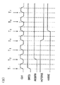
図2は、読み出し動作中のPCIバスインターフェースにおける種々の信号を示すタイミング図である。PCIバスを介してデータが伝送される周期は、バストランザクションサイクル20として既知である。バストランザクションサイクル20は、アドレスサイクル22と、例えば、24a,24b,24cのような幾つかのデータサイクルとを有する。各々のデータサイクル24a,24b,24cについては、さらに、待機(wait)サイクル26a,26b,26cと、データ転送サイクル28a,28b,28cとに分割することができる。以下に、PCI仕様にしたがう制御信号を示すために、読み出し動作中のPCIバスインターフェースについて、簡単に説明する。
【0005】
サイクルT1の間には、データトランザクションの開始を示すFRAME信号が、イニシエータにより送信され、その一方で、開始アドレスが、該トランザクションに関するターゲット装置を突き止めるために、アドレスバスAD回線上に置かれる。その間に、読み出しコマンドが、CBE回線を介して伝送される。読み出しコマンドの配信(delivery)後に、バイトイネーブル信号がCBE回線上に置かれる。バイトイネーブル信号は、(24a,24b,24cを包含する)データサイクルの始めから終わりまで送信される。サイクルT2の間には、イニシエータが、データ送信のためにイニシエータの準備ができている状態を示すイニシエータレディ信号IRDYを提示する。しかしながら、ターゲット装置の準備がまだできていない。これにより、ターゲット装置はデータを準備する状態を保持し、その一方で、イニシエータは、データサイクル24aの待機サイクル26aにおいて不働(idle)となる。サイクルT3の間には、ターゲット装置が、伝送のために必要なデータを全て準備しており、これにより、ターゲットレディTRDY信号を送出する。したがって、データサイクル28aにおいては、IDRYおよびTRDYの両方がアウト状態となり、かつこれにより、イニシエータは、ターゲット装置からデータを読み出し始めることができる。サイクルT4の間には、ターゲット装置が、もはや、ターゲットレディTRDY信号を発行せず、最初の組のデータ送信の終了を信号で通信する。その間に、1組のデータがターゲット装置内部で準備される。再び、イニシエータが、データサイクル24b内の待機サイクル26bに入る。サイクルT5の間には、第2組のデータの準備ができていることを示すターゲットレディTRDY信号が発行される。第2組のデータは、IRDY信号およびTRDY信号の両方が発行される場合のサイクル28bにおいて、イニシエータにより準備ができている。サイクルT6におけるように、イニシエータが、ターゲット装置から全てのデータを読み出すのに十分な時間を有していなければ、IRDY信号は終了する。TRDYはいまだにアウト状態なので、待機サイクル26cは、イニシエータにより活性化される。サイクルT7におけるように、再びイニシエータの準備ができると、IRDY信号が再発行される。イニシエータは、IRDY信号およびTRDY信号の両方が発行される場合のデータ伝送サイクル28cの間において、ターゲット装置からデータを読み出し、これにより、単一の読み出し動作を完了する。
【0006】
従来のPCI仕様にしたがって適切なデータトランザクションを実行するためには、複雑な制御信号と、待機状態と、アービトレーション段階とを用いる必要がある。通常は、45〜50個までの信号ピンが、PCI仕様にしたがって要求される。概して、制御チップ間の内部トランザクションのために、複雑な手順は不要である。したがって、制御チップ間の内部トランザクションの高速化を図るためには、従来のPCI仕様を固守する簡略化されたトランザクション方法が必要とされる。
【0007】
しかしながら、PCの制御チップ間のトランザクションは、概して、PCI仕様により与えられる全ての複雑な機能を用いない。制御チップ間の動作は、通常は低下する。装置の統合が進むにつれて、制御チップについては単一のチップに統合することができ、かつ、さらに多くの機能がもたらされる。例えば、CPU、北側ブリッジ(north bridge)、南側ブリッジ(south bridge)が統合されて単一チップの形に形成される。したがって、チップパッケージのピンが非常に重要なソースとなる。制御チップ間のトランザクション速度を増加させるために、制御チップ間で用いるために簡略化された特有の仕様が必要とされる。
【0008】
【発明が解決しようとする課題】
本発明は、制御チップと、制御チップセット内の制御チップ間におけるデータトランザクション方法と、制御チップセット内の制御チップ間におけるバスアービトレーション方法とを提供する。したがって、制御チップセットの性能は向上し、かつ、制御チップ間における信号線の形式および数が減少する。
【0009】
本発明は、制御チップセットの、および、該制御チップセット内の制御チップ間におけるデータトランザクション方法を提供する。データまたはコマンドについては、いかなる待機サイクル、停止または再試行も伴わずに、連続的に伝送することができる。
【0010】
本発明は、制御チップセット、および、該制御チップセット内の制御チップ間におけるデータトランザクション方法を提供し、この場合には、待機状態とデータトランザクションサイクルと停止/再試行プロトコルとのための信号線は必要とされない。
【0011】
本発明は、アービトレーション時間を減少させることができる制御チップ間におけるバスアービトレーション方法を提供する。
【0012】
本発明は、バス許可(bus grant)信号線が必要とされない、制御チップ間におけるバスアービトレーション方法を提供する。
【0013】
【課題を解決するための手段】
本発明によれば、制御チップセットの制御チップのデータバッファは一定の大きさおよび数量を有する。さらに、読み出し/書き込みコマンドにしたがって、読み出し/書き込み確認応答コマンドが示され、これにより、制御チップは、制御チップ内のバッファの状態を、互いに検出することができる。制御チップはコマンドの存在を示す(assert)ときに、これに対応するデータを予め準備する必要がある。これにより、待機状態とデータトランザクションサイクルと停止/再試行プロトコルとをもたらすための信号線を削除することができる。したがって、コマンドまたはデータを、待機、停止または再試行なしで、連続的に伝送することができ、これにより、性能が向上する。
【0014】
本発明のバストランザクション方法によれば、制御チップは、通常は、バスを用いる権限(authority)を制御するが、他のチップは、バスを用いるためのより高い優先順位を有する。待機サイクルなしのバス仕様を伴って、バスを用いる権限をアービトレートすることを、迅速にかつ誤りなしに行うことができる。したがって、いかなるGNT信号線も必要とされず、かつ、アービトレーション時間が減少する。第2制御チップにより要求されたトランザクションは常に許可されているので、全体的な性能が向上する。
【0015】
前述の一般的な説明および以下の詳細な説明は、例示的なものであり、かつ、特許請求される本発明に関するさらなる説明をもたらすために意図されていることを理解すべきである。
【0016】
【発明の実施の形態】
添付の図面は、本発明のさらなる理解をもたらすために備えられており、かつ、本明細書に組み込まれ、かつ、本明細書の一部を構成している。
【0017】
本発明は、制御チップセット間における、または、制御チップセットのチップ間におけるトランザクション方法およびアービトレーション方法を提供し、該方法は、制御チップ間におけるデータトランザクションの効率性を促進することができる。すなわち、前記方法は、制御チップ間におけるバストランザクション処理を簡略化する。パーソナルコンピュータ(PC)のようなコンピュータシステム内において北側ブリッジと南側ブリッジとからなる制御チップセットが、本発明による好ましい実施形態を説明するための例として用いられる。従来のPCI仕様により定義されるように、45のコマンド信号線が、南側ブリッジと北側ブリッジとの間で通信するために必要とされる。しかしながら、本発明の好ましい実施形態においては、15のコマンド信号線のみが、PCI仕様により定義された元の45のコマンド信号線を置き換えるために必要とされる。新たに定義された本発明の15のコマンドは、VLINKコマンドと称される。
【0018】
図3および表1を参照すると、図3は、本発明の好ましい実施形態による制御チップセットのブロック図を概略的に示し、この図においては、制御チップセットの北側ブリッジと南側ブリッジとの間における制御信号線が、詳細に示されている。表1は、図3に示される各々の制御信号線の意味を記載している。例えば、制御チップセットは、北側ブリッジ30と南側ブリッジ32とを具備する。北側ブリッジ30と南側ブリッジ32との間の通信信号線は、PCI仕様による45の信号線から、本発明による15の信号線へ減少する。したがって、北側ブリッジ30および南側ブリッジ32のさらなる30(=45−15)ピンを、他の目的のために用いることができ、これにより、チップセットの機能が促進される。
【0019】
図3および表1に示されるように、元のPCI仕様により定義されるデータおよびアドレスバス(ADバス)は、予約されているが、8つの二方向信号線まで減少され、その一方で、CBE,FRAME,IRDY,TRDY,STOP,DEVSEL,REQ,およびGNT信号線は、二方向バイトイネーブル(BE)信号線と、(両方とも南側ブリッジにより駆動される)アップリンクコマンド信号線UPCMDおよびアップリンクストローブ信号線UPSTBと、(両方とも北側ブリッジにより駆動される)ダウンリンクコマンド信号線DNCMDおよびダウンリンクストローブ信号線DNSTBと、までに簡略化される。北側ブリッジ30および南側ブリッジ32の各々は、独立したコマンド信号線を駆動させ、これらの信号線は、両方とも、バスコマンドの存在を示すことができる。さらに、1つの制御チップにより、バスコマンドの存在が示されかつバスの権限が得られれば、該制御チップは、アドレスをADバス上で送信しかつこれに対応するデータ長を送信することができるか、または、データをADバス上で送信しかつ該データのためのバイトイネーブル信号をBE信号線上で送信することができる。
【表1】

図4は、本発明による、バスクロック信号(CLK)と、ストローブ信号(STB)と、データ転送用データ回線のビットタイムとの間におけるタイミングの関係を示す。図4に示されるように、1つのクロック周期は、2つのストローブクロック周期を具備する。すなわち、アップリンクストローブ信号およびダウンリンクストローブ信号がアクティブ状態である場合の周波数は、バスクロック信号の周波数の2倍である。ストローブ信号の立ち上がりエッジと立ち下がりエッジとにより定義された4つのビットタイム0〜3が存在する。したがって、4ビットデータが、各々のデータ回線上において4つのビットタイム0〜3を用いることにより得られ、かつ、バスコマンドが符号化される。したがって、各々のクロック周期中に8つのデータ回線を用いることにより32ビットデータが得られ、これは、従来のPCI仕様において32個のデータ回線を用いてデータが伝送されることに等しい。さらに、BE信号線がデータ長を表しているかのように、1〜16(4ビット)データ長情報が1クロック周期の範囲内で得られる。
【0021】
種々の形式のデータトランザクションが、アップリンクコマンドUPCMDとダウンリンクコマンドDNCMDとを用いて定義される。南側ブリッジにより駆動されるアップリンクコマンドUPCMDは、読み出し確認応答コマンド(NB(北側ブリッジ)からSB(南側ブリッジ)へ)C2PRA、書き込み確認応答コマンド(NBからSBへ)C2PWA、読み出しコマンドP2CR(SBからNBへ)、書き込みコマンドP2CW(SBからNBへ)、などを具備する。アップリンクコマンドとビットタイム符号化との関係は表2に記載されている。要求信号REQは、他のバスコマンドとは重複していないビットタイム0においてその存在が示されている。したがって、REQ信号については、いつでも、バスコマンドの存在が示される同じクロック周期においてさえも、送信することができる。北側ブリッジにより駆動されるダウンリンクコマンドDNCMDは、入力/出力読み出しコマンド(NBからSBへ)C2PIOR、メモリ読み出しコマンド(NBからSBへ)C2PMR、入力/出力書き込みコマンド(NBからSBへ)C2PIOW、メモリ書き込みコマンド(NBからSBへ)C2PMW、読み出し確認応答コマンド(SBからNBへ)P2CRA、書き込み確認応答コマンド(SBからNBへ)P2CWA、などを具備する。ダウンリンクコマンドとビットタイム符号化との関係は表3に記載されている。本発明においては、いかなる許可信号GNTも定義されない。
【0022】
北側ブリッジにより示されるコマンドおよび南側ブリッジにより示されるコマンドは、互いに対応している。南側ブリッジが、多数のP2CRおよび/またはP2CWの存在を順次的に示すと、北側ブリッジは、南側ブリッジにより存在を示されたP2CRおよび/またはP2CWコマンドに応答して、これに対応するP2CRAおよび/またはP2CWAコマンドの存在を順次的に示す必要がある。同様に、北側ブリッジが多数のC2PIOR,C2PMR,C2PIOW,C2PMWコマンドの存在を順次的に示すと、南側ブリッジは、北側ブリッジにより存在を示されたコマンドに応答して、これに対応するC2CRAおよび/またはC2CWAの存在を順次的に示す必要がある。さらに、好ましい実施形態において説明するように、制御チップにより存在を示された各々のコマンドに対応するデータを、予め準備する必要がある。例えば、南側ブリッジがP2CWコマンドの存在を示すときには、メモリに書き込むべきデータの準備ができている必要があり、かつ、北側ブリッジがP2CRAコマンドの存在を示すときには、メモリから南側ブリッジへ読み出しデータを転送するためのデータの準備ができている必要がある。したがって、伝送されたデータについては、遮断(interrupting)や待機を回避することができる。
【表2】
図5は、本発明による書き込みトランザクションのための好ましい実施形態による制御チップセットのブロック図を概略的に示している。制御チップセットは、例えば、第1制御チップと、第2制御チップとを具備する。パーソナルコンピュータの一般的な利用において、第1制御チップおよび第2制御チップは、北側ブリッジ500および南側ブリッジ600であってもよい。第1制御チップ(北側ブリッジ500)および第2制御チップ(南側ブリッジ600)は、特別に設計されたバスにより結合されており、該バスの制御信号は、本発明のVLINKである。北側ブリッジ500は、データ送受信機510と、ターゲットコントローラ(例えば、メモリコントローラ)520と、書き込みデータキュー525と、書き込みトランザクションキュー530とを具備する。南側ブリッジ600は、データ送受信機610と、書き込みバッファサイズレジスタ535と、書き込みバッファカウントレジスタ540と、書き込みトランザクション生成器545と、書き込みトランザクション記録回路550と、書き込み比較器555とを具備する。
【0024】
本発明のVLINK仕様を満たすデータ送受信機510は、直接的にVLINKバスに結合する。VLINKバスを介して、データ送受信機510は、多数の書き込みトランザクションを完了するために、データを受信しかつ伝送することができる。ある書き込みトランザクションは、南側ブリッジ600がP2CWコマンドと該P2CWコマンドに対応するデータとを送信し、かつ次に、北側ブリッジ500が該P2CWコマンドに応答するためにP2CWAコマンドの存在を示すものとして定義されている。書き込みトランザクションキュー530は、一時的に、多数のデータ長と、全ての書き込みトランザクションの書き込みアドレスとを、順次的に記憶する。書き込みトランザクションキュー530の深度(depth)は、北側ブリッジ500が処理できる書き込みトランザクションの最大総数を決定する。書き込みデータキュー525は、ターゲットコントローラ520へ送信するための、南側ブリッジ600からのデータを記憶する。書き込みデータキュー525の深度は、北側ブリッジ500が処理できる書き込みデータの最大数を決定する。ターゲットコントローラ520は、データを、書き込みアドレスおよびデータ長にしたがってデータを受信するターゲット(例えば、外部メモリ)へ送信する。前記書き込みアドレスおよびデータ長は、最初に書き込みトランザクションキュー530に記憶され、かつ、書き込みデータキュー525に記憶されたデータは、該書き込みアドレスおよびデータ長に対応している。第1データ送受信機510は、書き込み確認応答信号(P2CWAコマンド)を送信して、対応するトランザクションが終了したことを南側ブリッジ600に知らせる。次に、書き込みデータキュー525に記憶された対応データは解放され、かつ、解放された空間は、他のデータを記憶することができる。
【0025】
前記南側ブリッジ600の書き込みバッファカウントレジスタ540および書き込みバッファサイズレジスタ535は、北側ブリッジ500の書き込みトランザクションキュー530に記憶することができる書き込みトランザクションの最大数と、北側ブリッジ500の書き込みデータキュー525に記憶することができるデータの最大数とを、それぞれ記憶する。例えば、書き込みトランザクションキュー530において受容可能な書き込みトランザクションの最大数は4であり、かつ、書き込みデータキュー525において受容可能なデータの最大数は16である。書き込みトランザクションの最大数およびデータの最大数(すなわち、書き込みバッファカウントおよび書き込みバッファサイズ)という2つのパラメータについては、ブート(booting)中にBIOS(basic input output system)構成により設定することができるか、または、チップセットの設計中に確定することができる。
【0026】
前記データ送受信機610は、全ての書き込みトランザクションを完了すべく、VLINKバスを介してデータを受信しかつ伝送するために、VLINKバスと結合されている。データ送受信機610がP2CWAコマンドを受信すると、書き込みが成功しかつバッファが解放されたことを示す信号が、現在対応している書き込みトランザクションのデータ長を記憶する空間を解放するために、書き込みトランザクション記録回路550へ送信される。次の書き込みトランザクションの新たなデータ長、書き込みアドレス、およびデータが書き込みトランザクション生成器545により生成されると、新たなデータ長が、書き込みトランザクション記録回路550へ送信される。
【0027】
前記書き込みトランザクション記録回路550は、書き込みデータキュー525において用いられるデータ数と、書き込みトランザクションキュー530において用いられる書き込みトランザクション数とを計算することが可能である。その理由は、書き込みトランザクション記録回路550が、全ての書き込みトランザクションのデータ長を順次的に記憶し、かつ、北側ブリッジ500により存在を示されるP2CWAが、南側ブリッジ600により存在を示されるP2CWコマンドの順序にしたがって応答されるためである。これにより、南側ブリッジ600は、北側ブリッジ500内のキューにおけるバッファの状態を認識することができる。
【0028】
前記書き込みトランザクション記録回路550は、書き込みデータキュー525において用いられるデータ数と、書き込みトランザクションキュー530において用いられる書き込みトランザクション数とを、書き込み比較器555へ送信することができる。次に、書き込み比較器555は、受信されたデータを、書き込みバッファサイズレジスタ535に記憶された書き込みデータキュー525のデータの最大数と、かつ、書き込みバッファカウントレジスタ540に記憶された書き込みトランザクションキュー530の書き込みトランザクションの最大数と、それぞれ比較する。書き込み比較器555により受信されたデータが最大データ数および最大書き込みトランザクション数よりも少なければ、書き込み比較器555は、データ送受信機610に、他の書き込みトランザクションを送信する能力を承認する。
【0029】
図6は、本発明による読み出しトランザクションのための好ましい実施形態による制御チップセットのブロック図を概略的に示している。制御チップセットは、例えば、第1制御チップと、第2制御チップとを具備する。パーソナルコンピュータの一般的な利用において、第1制御チップおよび第2制御チップは、北側ブリッジ500および南側ブリッジ600であってもよい。第1制御チップ(北側ブリッジ)500および第2制御チップ(南側ブリッジ)600は、特別に設計されたバスにより結合されており、該バスの制御信号は、本発明のVLINKである。北側ブリッジ500は、データ送受信機510と、ターゲットコントローラ(例えば、メモリコントローラ)520と、読み出しデータキュー625と、読み出しトランザクションキュー630とを具備する。南側ブリッジ600は、データ送受信機610と、読み出しバッファサイズレジスタ635と、読み出しバッファカウントレジスタ640と、読み出しトランザクション生成器645と、読み出しトランザクション記録回路650と、読み出し比較器655とを具備する。
【0030】
本発明のVLINK仕様を満たすデータ送受信機510は、直接的にVLINKバスに結合する。VLINKバスを介して、データ送受信機510は、多数の読み出しトランザクションを完了するために、データを受信しかつ伝送することができる。ある読み出しトランザクションは、南側ブリッジ600がP2CRコマンドを送信し、かつ次に、北側ブリッジ500が、該P2CRコマンドに応答するために、P2CRAコマンドと、これに対応するデータとを送信するものとして定義されている。読み出しトランザクションキュー630は、一時的に、多数のデータ長と、全ての読み出しトランザクションの読み出しアドレスとを、順次的に記憶する。読み出しトランザクションキュー630の深度は、北側ブリッジ500が処理できる読み出しトランザクションの最大数を決定する。読み出しデータキュー625は、ターゲットコントローラからの多数の読み出しデータ(該データは、南側ブリッジ600へ送信される)を一時的に記憶する。読み出しデータキュー625の深度は、北側ブリッジ500が処理できる読み出しデータの最大数を決定する。ターゲットコントローラ520は、データを、ターゲット(例えば、外部メモリ)から読み出し、かつ次に、読み出しアドレスおよびデータ長にしたがって、読み出しデータキュー625に記憶する。前記読み出しアドレスおよびデータ長は、最初に読み出しトランザクションキュー630に記憶され、かつ、読み出しデータキュー625に記憶されたデータは、該読み出しアドレスおよびデータ長に対応している。第1データ送受信機510は、読み出し確認応答信号(P2CRAコマンド)と、読み出しデータキュー625に記憶された読み出しデータとを送信する。次に、読み出しデータキュー625に記憶された対応データは解放され、かつ、解放された空間は、他のデータを記憶することができる。
【0031】
前記南側ブリッジ600の読み出しバッファカウントレジスタ640および読み出しバッファサイズレジスタ635は、北側ブリッジ500の読み出しトランザクションキュー630に記憶することができる読み出しトランザクションの最大数と、北側ブリッジ500の読み出しデータキュー625に記憶することができるデータの最大数とを、それぞれ記憶する。例えば、読み出しトランザクションキュー630および読み出しバッファカウントレジスタ640に記憶することができる読み出しトランザクションの最大数は4であり、かつ、読み出しデータキュー625に記憶することができるデータの最大数は16である。読み出しバッファカウントおよび読み出しバッファサイズ、という2つのパラメータについては、ブート中にBIOS(basic input output system)構成により設定することができるか、または、チップセットの設計中に確定することができる。
【0032】
前記データ送受信機610は、全ての読み出しトランザクションを完了すべく、VLINKバスを介してデータを受信しかつ伝送するために、VLINKバスと結合されている。データ送受信機610がP2CRAコマンドを受信すると、読み出しが成功しかつバッファが解放されたことを示す信号が、現在対応している読み出しトランザクションのデータ長を記憶する空間を解放するために、読み出しトランザクション記録回路650へ送信される。次の読み出しトランザクションの新たなデータ長、読み出しアドレス、およびデータが読み出しトランザクション生成器645により生成されると、新たなデータ長が、読み出しトランザクション記録回路650へ送信される。
【0033】
前記読み出しトランザクション記録回路650は、読み出しデータキュー625において用いられるデータ数と、読み出しトランザクションキュー630において用いられる読み出しトランザクション数とを計算することが可能である。その理由は、読み出しトランザクション記録回路650が、全ての読み出しトランザクションのデータ長を順次的に記憶し、かつ、北側ブリッジ500により存在を示されるP2CRAが、南側ブリッジ600により存在を示されるP2CRコマンドの順序にしたがって応答されるためである。これにより、南側ブリッジ600は、北側ブリッジ500内のキューにおけるバッファの状態を認識することができる。
【0034】
前記読み出しトランザクション記録回路650は、読み出しデータキュー625において用いられるデータ数と、読み出しトランザクションキュー630において用いられる読み出しトランザクション数とを、読み出し比較器655へ送信することができる。次に、読み出し比較器655は、受信されたデータを、読み出しバッファサイズレジスタ635に記憶された読み出しデータキュー625のデータの最大数と、かつ、読み出しバッファカウントレジスタ640に記憶された読み出しトランザクションキュー630の読み出しトランザクションの最大数と、それぞれ比較する。読み出し比較器655により受信されたデータが最大データ数および最大読み出しトランザクション数よりも少なければ、読み出し比較器655は、データ送受信機610に、他の読み出しトランザクションを開始する能力を通知する。
【0035】
前記北側ブリッジおよび南側ブリッジは、それぞれ、第1制御チップセットおよび第2制御チップセットであり、かつ、これらのコマンドは、データを読み出すかまたは書き込むべく北側ブリッジを制御するために、南側ブリッジにより送信される。しかしながら、当業者には明白なように、北側ブリッジおよび南側ブリッジの両方が対応する構造を有することができ、かつこれにより、これらのコマンドは、南側ブリッジまたは北側ブリッジにより送信されることに制約されるものではない。すなわち、南側ブリッジおよび北側ブリッジが、それぞれ、第1制御チップセットおよび第2制御チップセットであってもよい。
【0036】
上述の説明は、北側ブリッジおよび南側ブリッジがVLINKバスを用いるための権限を得る方法について述べてはいない。以下のパラグラフは、本発明による、チップセット間におけるアービトレーション方法について述べている。本発明によれば、第1制御チップは、通常は、バスを用いるための権限を制御するが、第2制御チップは、バスを用いるための、より高い優先順位を有する。第2制御チップが、バスを用いるための要求信号の存在を示す場合に、第1制御チップは、直ちにバスの権限を第2制御チップに対して解放する必要があるか、または、該第1制御チップが現在のバスコマンドサイクルを終了した後に、直ちにバスの権限を第2制御チップに対して解放する必要がある。VLINKバスのような待機サイクルを伴わないバス仕様とともに、バスを用いる権限をアービトレートすることを、迅速に、かつ、誤りなしに行うことができる。
【0037】
本発明は、制御チップセット内におけるバスアービトレーションの方法に向けられている。制御チップセットは、(北側ブリッジのような)第1制御チップと、(南側ブリッジのような)第2制御チップとを具備することができる。データは、第1制御チップと第2制御チップとの間で、待機サイクルを伴わない(VLINKバスのような)バスを介して伝送される。このバスは、さらに、図3〜図6に示されるような共通の二方向バスを具備する。
【0038】
前記第2制御チップは、一定のクロック数と、コマンドが二方向バスを用いるクロック数とを有する全てのバスコマンドを知る必要がある。第2制御チップが、第1制御チップに対して(読み出しコマンドのような)第1コマンドの存在を示すときには、第2制御チップは、確認応答コマンドのクロック数と、第1制御チップにより存在を示される、第1コマンドに対応するデータのクロック数とを記憶する必要があり、この場合には、確認応答コマンドのクロック数および第1コマンドにより応答されるデータのクロック数は、第1コマンドに包含される情報により決定される。例えば、南側ブリッジが北側ブリッジへP2CRコマンドの存在を示せば、データ長が南側ブリッジにより検出され、かつ、VLINKバスは、待機サイクルを必要とせず、したがって、南側ブリッジは、P2CRAコマンドのクロック数および北側ブリッジにより送信されるデータのクロック数を知ることができる。
【0039】
前記第2制御チップがバスを用いる必要があるときには、該第2制御チップは、直接的にバス要求信号の存在を示す。第1制御チップがバス要求信号を検出する際に、かつ、第1制御チップが二方向バスを現在用いていなければ、第1制御チップは、バスの権限を第2制御チップへ解放し、かつ、二方向バスを駆動しない。しかし、第1制御チップが二方向バスを現在用いていれば、第1制御チップは、現在のバスコマンドおよびトランザクションを終了した後に、バスの権限を第2制御チップへ直ちに解放する。
【0040】
これに対し、第2制御チップがバス要求信号の存在を示せば、該第2制御チップは、二方向バスが第1制御チップにより現在用いられているかどうかを検出する。第1制御チップが二方向バスを現在用いていることを第2制御チップが検出しなければ、該第2制御チップは、所定のサイクルだけ待機し、かつ、二方向バスを連続的に検出する。次に、第2制御チップは、所定の待機サイクルの後に、二方向バスを駆動する。所定の待機サイクルの目的は、二方向バスを介して伝送された信号を遅延させることができることである。第1制御チップによりコマンドの存在が示されている間に該第1制御チップがバスを用いていないことを第2制御チップが検出することを回避されするために、さらに、第1制御チップおよび第2制御チップが二方向バスを同時に駆動することを回避するために、バスの権限を転送するための1クロック周期のターンアラウンドサイクルが存在する必要がある。
【0041】
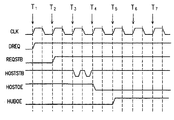
第1制御チップがバスを現在用いていることを第2制御チップが検出すると、南側ブリッジは、何のバスコマンドが第1制御チップにより現在実行されているのかと、バスコマンドを完了するために必要とされるクロック数とを検出することができる。次に、第2制御チップは、第1制御チップが現在のバスコマンドを完了した後にターンアラウンドサイクルだけ待機することにより、バスを駆動する。GNTコマンドを有する従来のバスアービトレーション方法においては、第1制御チップは、第2制御チップへGNTコマンドを駆動して、第2制御チップがバスを駆動し始めることができることを承認し、かつ次に、第2制御チップは、第1制御チップにより送信されたGNTコマンドを該第2制御チップが検出した後のターンアラウンドサイクル後に、バスを駆動する。図7(A)を参照すると、周期T1において、第2制御チップは、要求信号DREQの存在を示す。周期T2において、第2制御チップは、信号REQSTBの存在を示す。第1制御チップは、周期T4において、要求信号を受信し、かつ次に、バスを用いることができることを第2制御チップに承認するために、直ちにGNTコマンドの存在を示す。第1制御チップは、周期T5において、バスの駆動を停止する。周期T6において、第2制御チップは、GNT信号を受信し、かつ次に、バスを駆動し始める。これにより、バスの権限をアービトレートするための時間は、従来の方法にしたがってGNTコマンドを用いることにより浪費される。
【0042】
以下は、本発明の方法によるタイミングを説明するための幾つかの例である。図7(B)および図8〜図11は、バスの権限に対する許可と、バスの権限に関する要求とに関係するタイミング図を概略的に示している。以下の例において、南側ブリッジは、バスの使用のために要求信号の存在を示す。信号DREQは、南側ブリッジがバスを用いることを要求する内部信号を表す。信号DREQのハイレベルは、南側ブリッジがバスを内部的に用いることを要求していることを表す。信号REQSTBもまた内部信号であり、この信号においては、南側ブリッジが、REQSTBがハイレベルである場合に、アップリンクコマンド信号線UPCMDを用いて、ビットタイム0において、REQ信号の存在を示す。信号HOSTOEまたは信号HUBOEのハイレベルは、北側ブリッジまたは南側ブリッジが、バスを駆動させるためのバスの権限を得ることをそれぞれ表す。
【0043】
図7(B)を参照すると、周期T1において、信号DREQは、南側ブリッジがバスを用いる必要があることを意味するハイレベルに上昇する。周期T2において、要求ストローブ信号REQSTBは、ハイレベルに上昇し、かつ、南側ブリッジは、UPCMDを用いて、ビットタイム0において、真の要求信号REQの存在を示す。要求ストローブ信号REQSTBは、伝送の遅延に起因して、周期T4において受け入れられる。したがって、北側ブリッジがコマンドサイクルを開始すれば、該北側ブリッジは、周期T3において、ダウンリンクコマンドDNCMDの存在を示すことができる。また、南側ブリッジは、周期T5まで、コマンドサイクルを検出する。北側ブリッジがダウンリンクコマンドの存在を示さなければ、南側ブリッジは、周期T5において、BE/ADバスを用いる権限を有し、かつ、アップリンクコマンドの存在を示し、かつ、BE/ADバスを駆動する。この例においては、南側ブリッジは、周期T2において真のREQコマンドの存在を示し、かつ、ターンアラウンドサイクルを具備する所定のサイクル(3つのクロック数)だけ待機した後に、周期T5においてBE/ADバスを駆動する。
【0044】
図8を参照すると、周期T1において、信号DREQは、南側ブリッジがバスを用いる必要があることを意味するハイレベルに上昇する。周期T2において、信号REQSTBはハイレベルに上昇し、かつ次に、南側ブリッジは、アップリンクコマンド信号線UPCMDを介して、ビットタイム0において、真の要求信号REQの存在を示す。しかしながら、北側ブリッジは、周期T3において、P2CRAコマンドのようなダウンリンクコマンドの存在を示す。トランザクションに対応するデータ長が8ダブルワード(8DW)であると仮定する。8DWデータは、周期T3〜T10の間に転送される。南側ブリッジは、トランザクションのクロック数を知り、かつ、北側ブリッジがトランザクションの完了後にバスの権限を解放することを確認し、かつこれにより、南側ブリッジは、周期T11におけるターンアラウンドサイクル後の周期T12において、BE/ADバスを駆動することができる。
【0045】
図9を参照すると、周期T1において、DREQは、南側ブリッジがバスを用いる必要があることを表すハイレベルとなる。周期T2において、要求ストローブ信号REQSTBは、ハイレベルに変化し、かつ、南側ブリッジは、アップリンクコマンド信号線UPCMDを介して、ビットタイム0において、真の要求信号REQの存在を示す。しかしながら、北側ブリッジは、例えばC2PRコマンドのようなダウンリンクコマンドの存在を示す。C2PRコマンドのクロック数は、1クロック周期として固定され、周期T3において実行される。南側ブリッジは、一定の実行周期を有する全てのコマンドのクロック数を知り、かつ、北側ブリッジがバスの権限を解放することを確認する。これにより、南側ブリッジは、ターンアラウンドサイクル後の周期T5において、二方向BE,ADバスを駆動することができる。
【0046】
図10を参照すると、REQSTBがハイレベルであり、かつ、南側ブリッジがバスを用いることを許可されたと仮定する。南側ブリッジは、アップリンクコマンドUPCMDの存在を示し、かつ、二方向バスを駆動し始める。好ましい実施形態においては、2つの連続的なP2CRコマンドの存在が示され、かつ、周期T5,T6の間にデータが転送される。信号REQSTBは、周期T6において、ローレベルに変化する。すなわち、南側ブリッジがなおもバスを用いかつP2CRコマンドの存在を示すが、要求信号は、周期T6のビットタイム0において取り消されている。したがって、北側ブリッジは、南側ブリッジが、周期T8前にバスの使用要求を停止したことを検出し、かつ、周期T8においてBE/AD信号線を駆動する。
【0047】
図11を参照すると、周期T1において、北側ブリッジは、読み出しコマンドC2PRの存在を示す。南側ブリッジにより準備されたデータの用意ができたときに、南側ブリッジは、信号REQSTBをハイレベルとなるように駆動する。
所定の3クロック数だけ待機した後に、南側ブリッジは、ADバスを駆動して、周期T7において、北側ブリッジが要求するデータを送信し、かつ同時に、UPCMD信号線上でC2PRAコマンドの存在を示す。さらに、周期T7のビットタイム0において存在を示された要求信号REQは取り消され、かつ、北側ブリッジは、周期T9において、バスを用いる権限を得る。
【0048】
本発明の範囲から逸脱することなく、本発明の構成に対し、種々の変更がなされ得ることが、当業者には明白である。前述のことに鑑みて、本発明の修正および変更が、冒頭の特許請求の範囲およびそれらに均等なものの範囲内に収まれば、本発明は、前記修正および変更を包含するように意図されている。
【図面の簡単な説明】
【図1】従来のコンピュータシステムの種々の構成要素を接続しているPCIバスシステムを示すブロック図である。
【図2】読み出し動作中のPCIバスインターフェースにおける種々の信号を示すタイミング図である。
【図3】本発明の実施形態による、制御チップセットモジュール内部の制御チップ間におけるデータトランザクションにおいて用いられる制御信号を示すブロック図である。
【図4】本発明による、コマンド符号化のための4つのビットタイムを有するクロック周期を示す図である。
【図5】本発明による書き込みトランザクションのための好ましい実施形態による制御チップセットを概略的に示すブロック図である。
【図6】本発明による読み出しトランザクションのための好ましい実施形態による制御チップセットを概略的に示すブロック図である。
【図7】(A)は、従来のバスアービトレーション方法を示すタイミング図であり、(B)は、本発明によるバスアービトレーション方法の例を概略的に示す図である。
【図8】本発明によるバスアービトレーション方法の例を概略的に示す図である。
【図9】図8と同様の図である。
【図10】図8と同様の図である。
【図11】図8と同様の図である。
【符号の説明】
24 中央処理装置
30 北側ブリッジ
32 南側ブリッジ
36 メモリ
500 北側ブリッジ
510 データ送受信機
520 ターゲットコントローラ
525 書き込みデータキュー
530 書き込みトランザクションキュー
535 書き込みバッファサイズレジスタ
540 書き込みバッファカウントレジスタ
545 書き込みトランザクション生成器
550 書き込みトランザクション記録回路
555 書き込み比較器
600 南側ブリッジ
610 データ送受信機
625 読み出しデータキュー
630 読み出しトランザクションキュー
635 読み出しバッファサイズレジスタ
640 読み出しバッファカウントレジスタ
645 読み出しトランザクション生成器
650 読み出しトランザクション記録回路
655 読み出し比較器[0001]
BACKGROUND OF THE INVENTION
The present invention relates to a bus transaction method. More particularly, the present invention relates to a transaction method between control chipsets in a computer system.
[0002]
[Prior art]
FIG. 1 is a block diagram illustrating a PCI bus connecting various components of a conventional computer system. As shown in FIG. 1, the
[0003]
Data transmission between PCI compatible devices (such as the master controller of the control chipset or the north bridge) is controlled by a small number of interface control signals. A cycle frame (FRAME) is issued from an initiator (which may be the master controller or the north bridge) that indicates the start of the data access operation and its duration. As soon as the FRAME signal goes out, a data transaction via the PCI bus is started. The low side potential for the FRAME signal indicates that data transmission is in progress. After the start of the data transaction, the address bus AD sends out a valid address during the address cycle. Meanwhile, the command / byte enable (CBE [3: 0]) signal line sends a valid bus command (according to the PCI specification), which causes the target device to send data requested by the initiator. Know the transaction mode. Generally, 4 bits of the command / byte enable signal line can encode up to 16 different commands, and each command is defined in detail in the PCI specification. After the effective address goes out, a data cycle in which data is transmitted via the address bus AD is started. Meanwhile, a byte enable signal is transmitted, so that data can be transmitted. When transmission of the FRAME signal stops, the final set of data is transmitted and no further data is transmitted in the current transaction. Initiator ready (IRDY) and target ready (TRDY) signals are also used by the system to indicate the status of the initiator and target devices in the data transaction. . In a data read operation, the IRDY signal indicates that the initiator is ready to receive the requested data. In a data write operation, the TRDY signal indicates that the target device is ready to receive the requested data. The stop (STOP) signal is used by the target device to request the end of the data transaction from the initiator.
[0004]
FIG. 2 is a timing diagram showing various signals at the PCI bus interface during a read operation. The period in which data is transmitted over the PCI bus is known as the
[0005]
During cycle T1, a FRAME signal indicating the start of a data transaction is sent by the initiator, while the start address is placed on the address bus AD line to locate the target device for the transaction. In the meantime, a read command is transmitted via the CBE line. After delivery of the read command, a byte enable signal is placed on the CBE line. The byte enable signal is transmitted from the beginning to the end of the data cycle (including 24a, 24b, 24c). During cycle T2, the initiator presents an initiator ready signal IRDY indicating that the initiator is ready for data transmission. However, the target device is not ready yet. This keeps the target device ready for data, while the initiator is idle in the
[0006]
In order to execute an appropriate data transaction according to the conventional PCI specification, it is necessary to use complicated control signals, a standby state, and an arbitration stage. Typically, up to 45-50 signal pins are required according to the PCI specification. In general, complicated procedures are not required due to internal transactions between control chips. Therefore, in order to increase the speed of internal transactions between control chips, a simplified transaction method that adheres to the conventional PCI specifications is required.
[0007]
However, transactions between PC control chips generally do not use all the complex functions provided by the PCI specification. The operation between control chips is usually reduced. As device integration progresses, the control chip can be integrated into a single chip and provides more functionality. For example, a CPU, a north bridge, and a south bridge are integrated into a single chip. Therefore, the pin of the chip package is a very important source. In order to increase the transaction rate between control chips, simplified specific specifications are required for use between control chips.
[0008]
[Problems to be solved by the invention]
The present invention provides a control chip, a data transaction method between control chips in a control chip set, and a bus arbitration method between control chips in a control chip set. Therefore, the performance of the control chip set is improved, and the type and number of signal lines between the control chips are reduced.
[0009]
The present invention provides a data transaction method of a control chip set and between control chips in the control chip set. Data or commands can be transmitted continuously without any wait cycle, stop or retry.
[0010]
The present invention provides a control chipset and a method for data transaction between control chips in the control chipset, in which case signal lines for wait states, data transaction cycles and stop / retry protocols. Is not required.
[0011]
The present invention provides a bus arbitration method between control chips that can reduce arbitration time.
[0012]
The present invention provides a bus arbitration method between control chips that does not require a bus grant signal line.
[0013]
[Means for Solving the Problems]
According to the present invention, the data buffer of the control chip of the control chip set has a certain size and quantity. Furthermore, a read / write confirmation response command is indicated according to the read / write command, whereby the control chips can detect the states of the buffers in the control chip with each other. When the control chip indicates the presence of a command (assert), it is necessary to prepare data corresponding thereto. This eliminates signal lines for providing standby states, data transaction cycles, and stop / retry protocols. Thus, commands or data can be transmitted continuously without waiting, stopping or retrying, which improves performance.
[0014]
According to the bus transaction method of the present invention, the control chip normally controls the authority to use the bus, but the other chips have higher priority to use the bus. Arbitrating the authority to use the bus with a bus specification without a wait cycle can be done quickly and without error. Therefore, no GNT signal line is required and arbitration time is reduced. Since the transaction requested by the second control chip is always allowed, the overall performance is improved.
[0015]
It should be understood that the foregoing general description and the following detailed description are exemplary and are intended to provide further explanation of the claimed invention.
[0016]
DETAILED DESCRIPTION OF THE INVENTION
The accompanying drawings are included to provide a further understanding of the invention, and are incorporated in and constitute a part of this specification.
[0017]
The present invention provides a transaction method and arbitration method between control chipsets or between chips of a control chipset, which can facilitate the efficiency of data transactions between control chips. That is, the method simplifies bus transaction processing between control chips. A control chipset consisting of a north bridge and a south bridge in a computer system such as a personal computer (PC) is used as an example to illustrate a preferred embodiment according to the present invention. As defined by the conventional PCI specification, 45 command signal lines are required to communicate between the south bridge and the north bridge. However, in the preferred embodiment of the present invention, only 15 command signal lines are required to replace the original 45 command signal lines defined by the PCI specification. The 15 newly defined commands of the present invention are referred to as VLINK commands.
[0018]
Referring to FIG. 3 and Table 1, FIG. 3 schematically shows a block diagram of a control chipset according to a preferred embodiment of the present invention, in which between the north bridge and the south bridge of the control chipset The control signal line is shown in detail. Table 1 describes the meaning of each control signal line shown in FIG. For example, the control chipset includes a
[0019]
As shown in FIG. 3 and Table 1, the data and address bus (AD bus) defined by the original PCI specification is reserved but reduced to 8 bi-directional signal lines, while CBE , FRAME, IRDY, TRDY, STOP, DEVSEL, REQ, and GNT signal lines are bi-directional byte enable (BE) signal lines, uplink command signal lines UPCMD and uplink strobes (both driven by the south bridge). The signal line UPSTB is simplified to the downlink command signal line DNCMD and the downlink strobe signal line DNSTB (both driven by the north bridge). Each of
[Table 1]
FIG. 4 shows the timing relationship between the bus clock signal (CLK), the strobe signal (STB), and the bit time of the data line for data transfer according to the present invention. As shown in FIG. 4, one clock period comprises two strobe clock periods. That is, the frequency when the uplink strobe signal and the downlink strobe signal are in the active state is twice the frequency of the bus clock signal. There are four bit times 0 to 3 defined by the rising and falling edges of the strobe signal. Accordingly, 4-bit data is obtained by using four bit times 0-3 on each data line, and the bus command is encoded. Thus, 32 bits of data are obtained by using 8 data lines during each clock period, which is equivalent to transmitting data using 32 data lines in the conventional PCI specification. Furthermore, 1 to 16 (4 bits) data length information is obtained within a range of one clock cycle as if the BE signal line represents the data length.
[0021]
Various types of data transactions are defined using the uplink command UPCMD and the downlink command DNCMD. Uplink commands UPCMD driven by the south bridge are read acknowledge command (NB (north bridge) to SB (south bridge)) C2PRA, write acknowledge command (NB to SB) C2PWA, read command P2CR (from SB) NB), a write command P2CW (from SB to NB), and the like. The relationship between the uplink command and the bit time encoding is described in Table 2. The presence of the request signal REQ is indicated at bit time 0 which does not overlap with other bus commands. Thus, the REQ signal can be transmitted at any time, even in the same clock period where the presence of the bus command is indicated. Downlink command DNCMD driven by the north bridge is input / output read command (NB to SB) C2PIOR, memory read command (NB to SB) C2PMR, input / output write command (NB to SB) C2PIOW, memory A write command (NB to SB) C2PMW, a read confirmation response command (SB to NB) P2CRA, a write confirmation response command (SB to NB) P2CWA, and the like. The relationship between the downlink command and bittime encoding is described in Table 3. In the present invention, no grant signal GNT is defined.
[0022]
The command indicated by the north bridge and the command indicated by the south bridge correspond to each other. When the south bridge sequentially indicates the presence of multiple P2CRs and / or P2CWs, the north bridge responds to P2CR and / or P2CW commands indicated by the south bridge in response to the corresponding P2CRA and / or Or it is necessary to indicate the existence of the P2CWA command sequentially. Similarly, if the north bridge sequentially indicates the presence of a number of C2PIOR, C2PMR, C2PIOW, C2PMW commands, the south bridge responds to the commands indicated by the north bridge in response to the corresponding C2CRA and / or Or it is necessary to indicate the existence of C2CWA sequentially. Furthermore, as described in the preferred embodiment, data corresponding to each command indicated by the control chip needs to be prepared in advance. For example, when the south bridge indicates the presence of a P2CW command, the data to be written to memory must be ready, and when the north bridge indicates the presence of a P2CRA command, the read data is transferred from the memory to the south bridge. You need to be ready for data. Therefore, interrupting and waiting can be avoided for the transmitted data.
[Table 2]
FIG. 5 schematically shows a block diagram of a control chipset according to a preferred embodiment for a write transaction according to the present invention. The control chip set includes, for example, a first control chip and a second control chip. In a general use of a personal computer, the first control chip and the second control chip may be the
[0024]
A
[0025]
The write
[0026]
The
[0027]
The write
[0028]
The write
[0029]
FIG. 6 schematically shows a block diagram of a control chipset according to a preferred embodiment for a read transaction according to the present invention. The control chip set includes, for example, a first control chip and a second control chip. In a general use of a personal computer, the first control chip and the second control chip may be the
[0030]
A
[0031]
The read
[0032]
The
[0033]
The read
[0034]
The read
[0035]
The north bridge and south bridge are a first control chipset and a second control chipset, respectively, and these commands are transmitted by the south bridge to control the north bridge to read or write data. Is done. However, as will be apparent to those skilled in the art, both the north and south bridges can have a corresponding structure, and this limits these commands to be transmitted by the south or north bridge. It is not something. That is, the south side bridge and the north side bridge may be the first control chip set and the second control chip set, respectively.
[0036]
The above description does not describe how the north and south bridges are authorized to use the VLINK bus. The following paragraphs describe a method of arbitration between chipsets according to the present invention. According to the present invention, the first control chip normally controls the authority to use the bus, while the second control chip has a higher priority for using the bus. If the second control chip indicates the presence of a request signal to use the bus, the first control chip needs to immediately release the authority of the bus to the second control chip, or the first control chip Immediately after the control chip finishes the current bus command cycle, the bus authority needs to be released to the second control chip. Arbitrating the authority to use the bus along with a bus specification that does not involve a standby cycle such as the VLINK bus can be done quickly and without error.
[0037]
The present invention is directed to a method of bus arbitration within a control chipset. The control chipset can comprise a first control chip (such as the north bridge) and a second control chip (such as the south bridge). Data is transmitted between the first control chip and the second control chip via a bus (such as the VLINK bus) without a wait cycle. This bus further comprises a common bi-directional bus as shown in FIGS.
[0038]
The second control chip needs to know all bus commands that have a fixed number of clocks and a clock number of commands that use a bi-directional bus. When the second control chip indicates the presence of the first command (such as a read command) to the first control chip, the second control chip indicates the presence of the acknowledgment command clock number and the first control chip. Indicated The Data corresponding to the first command Number of clocks In this case, the number of clocks of the acknowledgment command and the response by the first command Ru The number of clocks of data is determined by information included in the first command. For example, if the south bridge indicates the presence of a P2CR command to the north bridge, the data length is detected by the south bridge, and the VLINK bus does not require a wait cycle, so the south bridge does not need the number of P2CRA command clocks and Sent by the north bridge Ru data Number of clocks Can know.
[0039]
When the second control chip needs to use a bus, the second control chip directly indicates the presence of a bus request signal. When the first control chip detects the bus request signal and if the first control chip is not currently using the bi-directional bus, the first control chip releases the authority of the bus to the second control chip; and Do not drive the two-way bus. However, if the first control chip is currently using a two-way bus, the first control chip immediately releases the bus authority to the second control chip after completing the current bus command and transaction.
[0040]
On the other hand, if the second control chip indicates the presence of the bus request signal, the second control chip detects whether the bi-directional bus is currently being used by the first control chip. If the second control chip does not detect that the first control chip is currently using the two-way bus, the second control chip waits for a predetermined cycle and continuously detects the two-way bus. . The second control chip then drives the bi-directional bus after a predetermined standby cycle. The purpose of a given waiting cycle is to be able to delay the signal transmitted over the two-way bus. In order to prevent the second control chip from detecting that the first control chip is not using the bus while the first control chip indicates the presence of a command, the first control chip and In order to avoid the second control chip driving the bi-directional bus at the same time, there must be a turnaround cycle of one clock period for transferring the authority of the bus.
[0041]
When the second control chip detects that the first control chip is currently using the bus, the south bridge is in order to complete what bus command is currently being executed by the first control chip and the bus command. The required number of clocks can be detected. The second control chip then drives the bus by waiting for a turnaround cycle after the first control chip completes the current bus command. In a conventional bus arbitration method with a GNT command, the first control chip drives the GNT command to the second control chip to acknowledge that the second control chip can begin driving the bus, and then The second control chip drives the bus after a turnaround cycle after the second control chip detects the GNT command transmitted by the first control chip. Referring to FIG. 7A, in the period T1, the second control chip indicates the presence of the request signal DREQ. In period T2, the second control chip indicates the presence of signal REQSTB. The first control chip receives a request signal in period T4 and then immediately indicates the presence of a GNT command to acknowledge to the second control chip that the bus can be used. The first control chip stops driving the bus in period T5. In period T6, the second control chip receives the GNT signal and then starts to drive the bus. Thus, the time to arbitrate bus authority is wasted by using GNT commands according to conventional methods.
[0042]
The following are some examples to illustrate timing according to the method of the present invention. FIGS. 7B and 8-11 schematically illustrate timing diagrams relating to authorization for bus authority and requests relating to bus authority. In the following example, the south bridge indicates the presence of a request signal for bus use. The signal DREQ represents an internal signal requesting that the south bridge use the bus. A high level of signal DREQ indicates that the south bridge is requesting that the bus be used internally. The signal REQSTB is also an internal signal, in which the south bridge indicates the presence of the REQ signal at bit time 0 using the uplink command signal line UPCMD when REQSTB is high. A high level of signal HOSTOE or signal HUBOE indicates that the north bridge or the south bridge obtains the authority of the bus to drive the bus, respectively.
[0043]
Referring to FIG. 7B, in period T1, signal DREQ rises to a high level, which means that the south bridge needs to use the bus. In period T2, the request strobe signal REQSTB rises to a high level, and the south bridge indicates the presence of a true request signal REQ at bit time 0 using UPCMD. The request strobe signal REQSTB is accepted in period T4 due to transmission delay. Therefore, if the north bridge starts a command cycle, the north bridge can indicate the presence of the downlink command DNCMD in period T3. Further, the south bridge detects a command cycle until the period T5. If the north bridge does not indicate the presence of a downlink command, the south bridge has authority to use the BE / AD bus in period T5, indicates the presence of an uplink command, and drives the BE / AD bus. To do. In this example, the south bridge indicates the presence of a true REQ command in period T2, and after waiting for a predetermined cycle (three clocks) with a turnaround cycle, the BE / AD bus in period T5. Drive.
[0044]
Referring to FIG. 8, in period T1, signal DREQ rises to a high level, which means that the south bridge needs to use the bus. In period T2, signal REQSTB rises to a high level, and then the south bridge indicates the presence of a true request signal REQ at bit time 0 via the uplink command signal line UPCMD. However, the north bridge indicates the presence of a downlink command, such as a P2CRA command, in period T3. Assume that the data length corresponding to the transaction is 8 double words (8 DW). The 8DW data is transferred during the period T3 to T10. The south bridge knows the number of clocks in the transaction and confirms that the north bridge releases the bus authority after the transaction is complete, and thus the south bridge is in period T12 after the turnaround cycle in period T11. The BE / AD bus can be driven.
[0045]
Referring to FIG. 9, in period T1, DREQ is at a high level indicating that the south bridge needs to use the bus. In period T2, the request strobe signal REQSTB changes to high level, and the south bridge indicates the presence of the true request signal REQ at bit time 0 via the uplink command signal line UPCMD. However, the north bridge indicates the presence of a downlink command such as a C2PR command. The number of clocks of the C2PR command is fixed as one clock period and is executed in the period T3. The south bridge knows the number of clocks of all commands with a certain execution period and confirms that the north bridge releases the bus authority. Thereby, the south side bridge can drive the bi-directional BE and AD buses in the period T5 after the turnaround cycle.
[0046]
Referring to FIG. 10, assume that REQSTB is high and the south bridge is authorized to use the bus. The south bridge indicates the presence of the uplink command UPCMD and begins to drive the bi-directional bus. In the preferred embodiment, the presence of two consecutive P2CR commands is indicated and data is transferred during periods T5, T6. The signal REQUSTB changes to a low level in the period T6. That is, the south bridge still uses the bus and indicates the presence of a P2CR command, but the request signal is canceled at bit time 0 of period T6. Therefore, the north side bridge detects that the south side bridge has stopped using the bus before the period T8, and drives the BE / AD signal line in the period T8.
[0047]
Referring to FIG. 11, in the period T1, the north bridge indicates the presence of the read command C2PR. When the data prepared by the south bridge is ready, the south bridge drives the signal REQSTB to be high level.
After waiting for a predetermined number of three clocks, the south bridge drives the AD bus, transmits data requested by the north bridge in period T7, and simultaneously indicates the presence of the C2PRA command on the UPCMD signal line. Further, the request signal REQ indicated to exist at the bit time 0 of the period T7 is canceled, and the north bridge is authorized to use the bus in the period T9.
[0048]
It will be apparent to those skilled in the art that various modifications can be made to the structure of the present invention without departing from the scope of the invention. In view of the foregoing, it is intended that the present invention cover the modifications and variations of this invention provided they come within the scope of the appended claims and their equivalents. .
[Brief description of the drawings]
FIG. 1 is a block diagram illustrating a PCI bus system connecting various components of a conventional computer system.
FIG. 2 is a timing diagram showing various signals at the PCI bus interface during a read operation.
FIG. 3 is a block diagram illustrating control signals used in a data transaction between control chips within a control chipset module according to an embodiment of the present invention.
FIG. 4 shows a clock cycle with four bit times for command coding according to the present invention.
FIG. 5 is a block diagram schematically illustrating a control chipset according to a preferred embodiment for a write transaction according to the present invention.
FIG. 6 is a block diagram schematically illustrating a control chipset according to a preferred embodiment for a read transaction according to the present invention.
FIG. 7A is a timing diagram illustrating a conventional bus arbitration method, and FIG. 7B is a diagram schematically illustrating an example of a bus arbitration method according to the present invention.
FIG. 8 is a diagram schematically showing an example of a bus arbitration method according to the present invention.
FIG. 9 is a view similar to FIG.
10 is a view similar to FIG.
11 is a view similar to FIG.
[Explanation of symbols]
24 Central processing unit
30 North Bridge
32 South Bridge
36 memory
500 North Bridge
510 Data transceiver
520 Target controller
525 Write data queue
530 Write transaction queue
535 Write buffer size register
540 Write buffer count register
545 Write Transaction Generator
550 write transaction recording circuit
555 Write Comparator
600 South Bridge
610 Data transceiver
625 Read data queue
630 Read transaction queue
635 Read buffer size register
640 Read buffer count register
645 Read transaction generator
650 read transaction recording circuit
655 readout comparator
Claims (8)
前記第2制御チップは、該第2制御チップがバスを用いる必要がある場合に、バス要求信号を送出する段階と、
前記第1制御チップは、該第1制御チップが要求信号を検出すれば、該第1制御チップが現在バスを用いていなければバスの権限を第2制御チップへ解放し、該第1制御チップが現在バスを用いていれば該第1制御チップが現在のバストランザクションを完了した後にバスの権限を第2制御チップへ直ちに解放する段階と、
前記第2制御チップは、前記第1制御チップが現在はバスを用いていないことを該第2制御チップが検出した場合に、所定時間の間待機した後にバスを使用する段階と、
前記第2制御チップは、前記第1制御チップが現在はバスを用いていることを該第2制御チップが検出した場合に、前記第1制御チップが現在に実行するバスコマンドと当該バスコマンドに必要とされるクロック数により、現在に実行するバスコマンドが完了され、かつターンアラウンドサイクルを待機した後に、バスを使用する段階と、
を具備することを特徴とする方法。The control chip set includes a first control chip and a second control chip, data is transferred between the first and second control chips via a bus, and the bus includes a bi-directional bus. A bus arbitration method in a control chip set,
The second control chip sends a bus request signal when the second control chip needs to use a bus;
If the first control chip detects a request signal, the first control chip releases the authority of the bus to the second control chip if the first control chip is not currently using the bus, and the first control chip Immediately releasing the authority of the bus to the second control chip after the first control chip completes the current bus transaction if
The second control chip uses the bus after waiting for a predetermined time when the second control chip detects that the first control chip is not currently using the bus;
When the second control chip detects that the first control chip is currently using a bus, the second control chip receives a bus command currently executed by the first control chip and the bus command. Using the bus after the currently executed bus command is completed and waiting for the turnaround cycle, depending on the number of clocks required; and
A method comprising the steps of:
前記第1制御チップは、現在のバスコマンドを実行するためのクロック数と、現在のバスコマンドに対応するデータ送信のために二方向バスを用いるクロック数とを、前記第2制御チップへ供給する段階と、
前記第2制御チップは、該第2制御チップが第1制御チップに対してコマンドを送出する場合に、確認応答のクロック数と、前記コマンドに対応する前記第1制御チップにより応答されるデータのクロック数とを記憶する段階と、
をさらに具備し、前記確認応答のクロック数と、前記第1制御チップにより応答されるデータのクロック数とは、前記確認応答が送信されるべき、前記コマンドに予め格納されているクロック数、及びデータが送信されるべき、前記コマンドに予め格納されているクロック数に基づいてコマンドにより決定されることを特徴とする請求項1に記載の方法。In order to calculate the waiting time before the second control chip drives the bus when the second control chip detects that the first control chip is currently using the bus,
The first control chip supplies a clock number for executing a current bus command and a clock number using a bidirectional bus for data transmission corresponding to the current bus command to the second control chip. Stages,
The second control chip, when the second control chip sends a command to the first control chip, confirmed the clock number of the response, the data that will be answered by the first control chip corresponding to the command Storing the number of clocks ;
Further comprising a clock speed of said acknowledgment, said the clock number of the data that will be answered by the first control chip, the confirmation response should be transmitted, the number of clocks stored in advance in said command, and The method of claim 1 , wherein data is determined by a command based on a number of clocks previously stored in the command to be transmitted.
Applications Claiming Priority (2)
| Application Number | Priority Date | Filing Date | Title |
|---|---|---|---|
| TW88121973 | 1999-12-15 | ||
| TW088121973A TW468112B (en) | 1999-12-15 | 1999-12-15 | Arbitrating method of bus between control chipsets |
Publications (3)
| Publication Number | Publication Date |
|---|---|
| JP2001216254A JP2001216254A (en) | 2001-08-10 |
| JP2001216254A5 JP2001216254A5 (en) | 2010-08-19 |
| JP4583590B2 true JP4583590B2 (en) | 2010-11-17 |
Family
ID=21643386
Family Applications (1)
| Application Number | Title | Priority Date | Filing Date |
|---|---|---|---|
| JP2000379455A Expired - Lifetime JP4583590B2 (en) | 1999-12-15 | 2000-12-13 | Control chipset arbitration in bus transactions |
Country Status (4)
| Country | Link |
|---|---|
| US (1) | US6721833B2 (en) |
| JP (1) | JP4583590B2 (en) |
| DE (1) | DE10061770B4 (en) |
| TW (1) | TW468112B (en) |
Families Citing this family (11)
| Publication number | Priority date | Publication date | Assignee | Title |
|---|---|---|---|---|
| US7085866B1 (en) * | 2002-02-19 | 2006-08-01 | Hobson Richard F | Hierarchical bus structure and memory access protocol for multiprocessor systems |
| US6959372B1 (en) * | 2002-02-19 | 2005-10-25 | Cogent Chipware Inc. | Processor cluster architecture and associated parallel processing methods |
| JP2005250671A (en) * | 2004-03-02 | 2005-09-15 | Sony Corp | Communication system, communication apparatus, communication method and program |
| CN100336045C (en) * | 2004-11-19 | 2007-09-05 | 威盛电子股份有限公司 | Multifunction chip set and relative method |
| US7174403B2 (en) * | 2005-02-24 | 2007-02-06 | Qualcomm Incorporated | Plural bus arbitrations per cycle via higher-frequency arbiter |
| US20060277444A1 (en) * | 2005-06-03 | 2006-12-07 | Nicholas Holian | Recordation of error information |
| US7467245B2 (en) * | 2005-07-22 | 2008-12-16 | Cisco Technology, Inc. | PCI arbiter |
| US7757031B2 (en) * | 2005-10-24 | 2010-07-13 | Via Technologies, Inc. | Data transmission coordinating method and system |
| US7945719B2 (en) | 2006-09-20 | 2011-05-17 | Intel Corporation | Controller link for manageability engine |
| CN104978302B (en) * | 2015-06-24 | 2018-02-23 | 山东超越数控电子股份有限公司 | A kind of intelligent and safe USB interface control method based on TCM chips |
| TWI637269B (en) * | 2017-12-26 | 2018-10-01 | 奇景光電股份有限公司 | Electronic apparatus and operation method thereof |
Family Cites Families (11)
| Publication number | Priority date | Publication date | Assignee | Title |
|---|---|---|---|---|
| JPH05324544A (en) * | 1992-05-15 | 1993-12-07 | Hitachi Ltd | Bus control method |
| TW242183B (en) * | 1993-11-26 | 1995-03-01 | United Microelectronics Corp | Chip set architecture for personal computer |
| TW400483B (en) * | 1994-03-01 | 2000-08-01 | Intel Corp | High performance symmetric arbitration protocol with support for I/O requirements |
| US5787264A (en) * | 1995-05-08 | 1998-07-28 | Apple Computer, Inc. | Method and apparatus for arbitrating access to a shared bus |
| US6058443A (en) * | 1997-02-18 | 2000-05-02 | Advanced Micro Devices, Inc. | System for partitioning PC chipset functions into logic and port integrated circuits |
| US6073199A (en) * | 1997-10-06 | 2000-06-06 | Cisco Technology, Inc. | History-based bus arbitration with hidden re-arbitration during wait cycles |
| US6195722B1 (en) * | 1998-01-26 | 2001-02-27 | Intel Corporation | Method and apparatus for deferring transactions on a host bus having a third party agent |
| US6202112B1 (en) * | 1998-12-03 | 2001-03-13 | Intel Corporation | Arbitration methods to avoid deadlock and livelock when performing transactions across a bridge |
| US6223244B1 (en) * | 1998-12-10 | 2001-04-24 | International Business Machines Corporation | Method for assuring device access to a bus having a fixed priority arbitration scheme |
| US6253270B1 (en) * | 1998-12-30 | 2001-06-26 | Intel Corporation | Method and apparatus for arbitrating ownership of an interface between hub agents |
| US6347351B1 (en) * | 1999-11-03 | 2002-02-12 | Intel Corporation | Method and apparatus for supporting multi-clock propagation in a computer system having a point to point half duplex interconnect |
-
1999
- 1999-12-15 TW TW088121973A patent/TW468112B/en not_active IP Right Cessation
-
2000
- 2000-12-12 US US09/735,412 patent/US6721833B2/en not_active Expired - Lifetime
- 2000-12-12 DE DE10061770A patent/DE10061770B4/en not_active Expired - Lifetime
- 2000-12-13 JP JP2000379455A patent/JP4583590B2/en not_active Expired - Lifetime
Also Published As
| Publication number | Publication date |
|---|---|
| US20010004749A1 (en) | 2001-06-21 |
| DE10061770B4 (en) | 2007-11-08 |
| JP2001216254A (en) | 2001-08-10 |
| TW468112B (en) | 2001-12-11 |
| DE10061770A1 (en) | 2001-08-09 |
| US6721833B2 (en) | 2004-04-13 |
Similar Documents
| Publication | Publication Date | Title |
|---|---|---|
| KR970000842B1 (en) | System direct memory access(dma)support logic for pci based computer system | |
| US5634138A (en) | Burst broadcasting on a peripheral component interconnect bus | |
| US6772254B2 (en) | Multi-master computer system with overlapped read and write operations and scalable address pipelining | |
| US5191656A (en) | Method and apparatus for shared use of a multiplexed address/data signal bus by multiple bus masters | |
| US5398244A (en) | Method and apparatus for reduced latency in hold bus cycles | |
| US5584033A (en) | Apparatus and method for burst data transfer employing a pause at fixed data intervals | |
| KR100267130B1 (en) | Pci bus system | |
| JPH08227392A (en) | Bus system with waiting time and shadow timer | |
| JP4583590B2 (en) | Control chipset arbitration in bus transactions | |
| KR930002787B1 (en) | Universal peripheral controller self-configuring bootloadable ramware | |
| US6697904B1 (en) | Preventing starvation of agents on a bus bridge | |
| US7096290B2 (en) | On-chip high speed data interface | |
| JP3602435B2 (en) | Data transaction method between control chipsets | |
| US5150466A (en) | Flexible distributed bus priority network | |
| US5974488A (en) | Method and apparatus for transmission of signals over a shared line | |
| JP4011258B2 (en) | Arbitration method of bus having interrupt function between control chip sets | |
| JPH0981507A (en) | Computer system | |
| JP4499235B2 (en) | PCI bus compatible masters and arbiters and arbitration methods | |
| US6327636B1 (en) | Ordering for pipelined read transfers | |
| US6178477B1 (en) | Method and system for pseudo delayed transactions through a bridge to guarantee access to a shared resource | |
| US6240474B1 (en) | Pipelined read transfers | |
| US7107374B1 (en) | Method for bus mastering for devices resident in configurable system logic | |
| JP5146796B2 (en) | Host controller | |
| JP2000267991A (en) | Retry processing method in reading processing of bus | |
| JPH03225458A (en) | Dma control system |
Legal Events
| Date | Code | Title | Description |
|---|---|---|---|
| A977 | Report on retrieval |
Free format text: JAPANESE INTERMEDIATE CODE: A971007 Effective date: 20060616 |
|
| A131 | Notification of reasons for refusal |
Free format text: JAPANESE INTERMEDIATE CODE: A131 Effective date: 20060704 |
|
| A521 | Request for written amendment filed |
Free format text: JAPANESE INTERMEDIATE CODE: A523 Effective date: 20061003 |
|
| A02 | Decision of refusal |
Free format text: JAPANESE INTERMEDIATE CODE: A02 Effective date: 20070417 |
|
| A521 | Request for written amendment filed |
Free format text: JAPANESE INTERMEDIATE CODE: A523 Effective date: 20070815 |
|
| A911 | Transfer to examiner for re-examination before appeal (zenchi) |
Free format text: JAPANESE INTERMEDIATE CODE: A911 Effective date: 20070821 |
|
| A912 | Re-examination (zenchi) completed and case transferred to appeal board |
Free format text: JAPANESE INTERMEDIATE CODE: A912 Effective date: 20080905 |
|
| A524 | Written submission of copy of amendment under article 19 pct |
Free format text: JAPANESE INTERMEDIATE CODE: A524 Effective date: 20100707 |
|
| A01 | Written decision to grant a patent or to grant a registration (utility model) |
Free format text: JAPANESE INTERMEDIATE CODE: A01 |
|
| A61 | First payment of annual fees (during grant procedure) |
Free format text: JAPANESE INTERMEDIATE CODE: A61 Effective date: 20100901 |
|
| R150 | Certificate of patent or registration of utility model |
Ref document number: 4583590 Country of ref document: JP Free format text: JAPANESE INTERMEDIATE CODE: R150 Free format text: JAPANESE INTERMEDIATE CODE: R150 |
|
| FPAY | Renewal fee payment (event date is renewal date of database) |
Free format text: PAYMENT UNTIL: 20130910 Year of fee payment: 3 |
|
| R250 | Receipt of annual fees |
Free format text: JAPANESE INTERMEDIATE CODE: R250 |
|
| R250 | Receipt of annual fees |
Free format text: JAPANESE INTERMEDIATE CODE: R250 |
|
| R250 | Receipt of annual fees |
Free format text: JAPANESE INTERMEDIATE CODE: R250 |
|
| R250 | Receipt of annual fees |
Free format text: JAPANESE INTERMEDIATE CODE: R250 |
|
| R250 | Receipt of annual fees |
Free format text: JAPANESE INTERMEDIATE CODE: R250 |
|
| R250 | Receipt of annual fees |
Free format text: JAPANESE INTERMEDIATE CODE: R250 |
|
| R250 | Receipt of annual fees |
Free format text: JAPANESE INTERMEDIATE CODE: R250 |
|
| R250 | Receipt of annual fees |
Free format text: JAPANESE INTERMEDIATE CODE: R250 |
|
| EXPY | Cancellation because of completion of term |