JP4579670B2 - Parts crimping apparatus and crimping method - Google Patents
Parts crimping apparatus and crimping method Download PDFInfo
- Publication number
- JP4579670B2 JP4579670B2 JP2004364745A JP2004364745A JP4579670B2 JP 4579670 B2 JP4579670 B2 JP 4579670B2 JP 2004364745 A JP2004364745 A JP 2004364745A JP 2004364745 A JP2004364745 A JP 2004364745A JP 4579670 B2 JP4579670 B2 JP 4579670B2
- Authority
- JP
- Japan
- Prior art keywords
- crimping
- circuit board
- display panel
- electronic component
- arm body
- Prior art date
- Legal status (The legal status is an assumption and is not a legal conclusion. Google has not performed a legal analysis and makes no representation as to the accuracy of the status listed.)
- Active
Links
Images


Description
この発明はたとえば液晶パネルに電子部品を介して回路基板を接続する部品の圧着装置及び圧着方法に関する。 The present invention relates to a component crimping apparatus and a crimping method for connecting a circuit board to a liquid crystal panel via an electronic component, for example.
液晶方式の表示装置の組立工程では、たとえば図8(a)に示すように、まずアウタリードボンダにより液晶パネル200の外周の4辺のうちの所定の辺に、液晶駆動用ICが搭載された第2の部品としてのタブ(TAB:Tape Automated Bonding)などの電子部品202を図8(c)に示すようにテープ状の異方性導電部材204を介して実装して電子部品付きの液晶パネル200を製造し、ついで電子部品付きの液晶パネル200の電子部品202の部分に対して図8(b)に示すように第1の部品としての回路基板203を電気的に接続して液晶パネル200を組み立てるということが行われている。上記回路基板203と電子部品202とは、図8(c)に示すように電子部品202と液晶パネル200との接続と同様、異方性導電部材204が用いられる。
In the assembly process of the liquid crystal display device, for example, as shown in FIG. 8A, first, a liquid crystal driving IC is mounted on a predetermined side of the outer periphery of the
図6は、液晶パネル200に予め接続された電子部品202に回路基板203を接続するために用いられる従来の圧着装置を示す概略的構成図である。この圧着装置には上記電子部品202を回路基板203に圧着する圧着位置Bに同図に矢印で示すX方向に沿って長い板状のバックアップツール101が設けられている。このバックアップツール101の上方には加圧ツール102が上下駆動可能、つまり同図に矢印で示すZ方向に駆動可能に設けられている。
FIG. 6 is a schematic configuration diagram showing a conventional crimping apparatus used for connecting the
電子部品202が予め圧着された液晶パネル200は搬送ステージ103に行列状に設けられた複数の吸着パッド104によって吸着保持されている。この搬送ステージ103はX、Y及びZ方向に駆動可能となっている。X方向は上記バックアップツールの長手方向に沿う方向であって、Y方向は同図に矢印で示すようにX方向に直交する方向である。
The
搬送ステージ103によって液晶パネル200を圧着位置Bに搬送する前に、この圧着位置Bには保持アーム体105が待機している。この保持アーム体105は基部106を有し、この基部106には基端を固定した複数のアーム107が上記バックアップツール101の長手方向に所定間隔で櫛刃状に設けられている。各アーム107には上記搬送ステージ103の吸着パッド104よりも背の低い複数の吸着パッド108が設けられている。上記保持アーム体105はY方向及びZ方向に駆動可能となっている。
Before the
同図中110は搬送アーム体110である。この搬送アーム体110は基部111に複数のアーム112が所定間隔で櫛刃状に設けられていて、各アーム112には複数の吸着パッド113が設けられている。この搬送アーム体110はX方向とZ方向に駆動可能であって、圧着作業が始まる前は、同図に示すようにバックアップツール101に対してX方向及びY方向に後退した位置で待機している。
In the figure,
図7(a)に示すように保持アーム体105が圧着位置Bで待機した状態で、液晶パネル200を保持した搬送ステージ103が同図に実線で示すように、上記圧着位置Bに近付くY方向に駆動される。
As shown in FIG. 7A, in the state where the
それによって、保持アーム体105の各アーム107が搬送ステージ103の吸着パッド104間に入り込み、液晶パネル200に接続された電子部品202が予めバックアップツール101上に位置決めされた回路基板203の異方性導電部材204が貼着された一端部の上方に位置決めされる。
これと同時に、搬送アーム体110は上記バックアップツール101と対向する位置まで同図に矢印で示すX方向に前進駆動されて待機する。
Thereby, each
At the same time, the
つぎに、上記搬送ステージ103が下降し、電子部品202の一端部が上記回路基板203の一端部の上面に重合するとともに、その状態で回路基板203が保持アーム体105に受け渡される。ついで、加圧ツール102が下降し、回路基板203と電子部品202との重合部分を加圧加熱する。それによって、異方性導電部材204が溶融硬化して回路基板203と電子部品202とが圧着される。
Next, the
上記加圧ツール102による加圧が開始されると、搬送ステージ103は保持アーム体105と干渉しない位置まで下降し、ついでX方向(Y方向にも駆動されることもある)に移動して液晶パネル200の供給部(図示せず)に戻る。供給部に戻った搬送ステージ103にはつぎの液晶パネル200が供給保持される。
When the pressurization by the
回路基板203と電子部品202との圧着が終了すると、上記保持アーム体105が上昇して電子部品202に圧着された回路基板203をバックアップツール101の上端面から浮上させた後、液晶パネル200とともに図7(b)に示すようにバックアップツール101から離れる、同図に矢印で示すY方向の後退方向に駆動される。
When the pressure bonding between the
上記保持アーム体105の後退位置には同図に実線で示すように搬送アーム体110が待機している。そのため、保持アーム体105がY方向に後退すると、そのアーム107が搬送アーム体110のアーム112間に入り込み、その吸着パッド108に保持された液晶パネル200が搬送アーム体110の吸着パッド113の上方に位置する。その状態で保持アーム体105が下降する。それによって、液晶パネル200は搬送アーム体110の吸着パッド113に受け渡される。
At the retracted position of the
液晶パネル200を搬送アーム体110に受け渡すと、保持アーム体105は図7(c)に示すようにY方向に前進して圧着位置Bに戻る。ついで、搬送アーム体110が同図に矢印で示すX方向の後退方向に駆動され、この搬送アーム体110に保持された液晶パネル200を次工程に受け渡す。
When the
上記搬送アーム体110がX方向の後退方向に駆動されると、新たな液晶パネル200が供給された搬送ステージ103が圧着位置Bに戻り、上述した工程が繰り返されることになる。
しかしながら、このような構成によると、回路基板203が液晶パネル200の電子部品202に圧着されたならば、圧着位置Bから保持アーム体105をY方向に後退させて液晶パネル200を搬送アーム体110に受け渡し、この搬送アーム体110をX方向に移動させて液晶パネル200を次工程に受け渡すことになる。
However, according to such a configuration, if the
そのため、回路基板203を液晶パネル200の電子部品202に圧着した後、保持アーム体105が圧着位置Bから後退し、液晶パネル200を搬送アーム体110に受け渡してから、上記圧着位置Bに戻らなければつぎの圧着作業、つまり新たな液晶パネルを保持した搬送ステージ103を圧着位置Bに移動させることができなかった。
Therefore, after the
そのため、回路基板203を液晶パネル200の電子部品202に圧着した後、つぎの液晶パネル200の電子部品202に回路基板203を圧着する作業に移行するまでに時間が掛かり、生産性の低下を招く一因となっていた。
Therefore, after the
つまり、液晶パネル200を保持アーム体105から搬送アーム体110に受け渡し、この搬送アーム体110をバックアップツール101に対向する位置から後退させてからでなければ、新たな液晶パネル200が供給された搬送ステージ103を圧着位置Bに戻ることができないため、サイクルタイムが長くなるということがあった。
In other words, the
この発明は、回路基板に表示パネルに接続された電子部品を圧着し、電子部品を介して接続された回路基板と表示パネルを圧着位置から搬出すると同時に、搬送ステージを圧着位置に戻してつぎの圧着作業を開始できるようにした部品の圧着装置及び圧着方法を提供することにある。 The present invention, crimp the electronic components connected to the circuit board to the display panel, and at the same time carrying out a connected circuit board and the display panel through the electronic component from the crimping position, the next return the carrier stage in crimping position An object of the present invention is to provide a component crimping apparatus and a crimping method capable of starting a crimping operation.
この発明は、圧着位置に回路基板と表示パネルに接続された電子部品とを位置決めし、これら回路基板と電子部品を圧着する部品の圧着装置であって、
予め上記圧着位置に位置決めされた上記回路基板に対し上記表示パネルに接続された電子部品を搬送位置決めする搬送ステージと、
この搬送ステージによって搬送された電子部品と上記回路基板を圧着する圧着手段と、
上記回路基板と電子部品を圧着している間に上記搬送ステージによって支持された上記表示パネルを受けて上記搬送ステージを退避可能とするとともに、上記圧着が終了したならば回路基板と表示パネルとを圧着位置から搬出して上記搬送ステージを圧着位置に移動可能にする搬送アーム体と
を具備したことを特徴とする部品の圧着装置にある。
The present invention is a component crimping apparatus that positions a circuit board and an electronic component connected to a display panel at a crimping position, and crimps the circuit board and the electronic component ,
A transport stage for transporting and positioning an electronic component connected to the display panel with respect to the circuit board previously positioned at the pressure-bonding position;
Crimping means for crimping the electronic component transported by the transport stage and the circuit board ;
While receiving the display panel supported by the transfer stage while crimping the circuit board and the electronic component , the transfer stage can be retracted, and when the crimping is completed, the circuit board and the display panel are moved. A component crimping apparatus comprising: a transport arm body that is unloaded from the crimping position and enables the transport stage to move to the crimping position.
上記回路基板と電子部品とは異方性導電部材によって接続固定されることが好ましい。 The circuit board and the electronic component are preferably connected and fixed by an anisotropic conductive member.
上記搬送アーム体は水平方向及び水平面に直交する軸線を中心とした回転方向に駆動可能であって、上記電子部品を介して接続された回路基板と表示パネルを上記圧着位置から搬出した後、回転駆動されることで上記回路基板と表示パネルとを方向変換可能であることが好ましい。 The transfer arm body can be driven in a horizontal direction and a rotation direction centering on an axis perpendicular to the horizontal plane, and the circuit board and the display panel connected via the electronic components are rotated from the crimping position and then rotated. It is preferable that the direction of the circuit board and the display panel can be changed by being driven.
この発明は、圧着位置に回路基板と表示パネルに接続された電子部品とを位置決めし、これら回路基板と電子部品を圧着する部品の圧着方法であって、
予め上記圧着位置に位置決めされた上記回路基板に対し上記表示パネルに接続された電子部品を搬送ステージによって搬送して位置決めする工程と、
圧着位置に搬送された表示パネルを上記搬送ステージによって支持しこの表示パネルに接続された電子部品と上記回路基板を圧着する工程と、
上記回路基板と電子部品を圧着している間に上記搬送ステージによって支持された上記表示パネルを搬送アーム体で受けて上記搬送ステージを退避させ、この搬送ステージに新たな表示パネルを供給する工程と、
上記圧着が終了したならば圧着された回路基板と表示パネルとを上記搬送アーム体によって上記圧着位置から搬出すると同時に、新たな表示パネルが供給された上記搬送ステージを圧着位置に移動させる工程と
を具備したことを特徴とする部品の圧着方法にある。
The present invention, positioning the connected electronic component on a circuit board and the display panel to the crimping position, a compression method of the part for crimping these circuit boards and electronic components,
A step of transporting and positioning an electronic component connected to the display panel with respect to the circuit board previously positioned at the crimping position by a transport stage;
A step of supporting the display panel transported to the crimping position by the transport stage and crimping the electronic component connected to the display panel and the circuit board ;
Receiving the display panel supported by the transfer stage while the circuit board and the electronic component are being crimped by a transfer arm body, retracting the transfer stage, and supplying a new display panel to the transfer stage; ,
When the crimping is finished, the crimped circuit board and the display panel are unloaded from the crimping position by the transport arm body, and at the same time, the transport stage supplied with a new display panel is moved to the crimping position. It is in the method of crimping a part characterized by comprising.
上記搬送ステージが表示パネルを上記圧着位置に供給する移動方向と、上記搬送ア−ム体が上記圧着位置から上記電子部品を介して接続された回路基板と表示パネルとを搬出する移動方向とは直交することが好ましい。 The moving direction in which the transfer stage supplies the display panel to the crimping position, and the moving direction in which the transfer arm body unloads the circuit board and the display panel connected via the electronic components from the crimping position. It is preferable to be orthogonal.
この発明によれば、圧着された回路基板と電子部品を介して接続された表示パネルとを搬送アーム体によって圧着位置から搬出すると同時に、新たな表示パネルが供給された搬送ステージを圧着位置に移動させることができるから、搬送ステージの待機時間が短縮され、生産性の向上を図ることができる。 According to the present invention, the circuit board that has been crimped and the display panel connected via the electronic component are carried out of the crimping position by the transport arm body, and at the same time, the transport stage supplied with the new display panel is moved to the crimping position. Therefore, the waiting time of the transfer stage is shortened, and productivity can be improved.
以下、この発明の一実施の形態を図1乃至図5を参照して説明する。
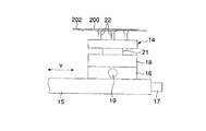
図1はこの発明の圧着装置の概略的構成を示す斜視図であって、この圧着装置は圧着位置Bにバックアップツール11が配設されている。このバックアップツール11は同図に矢印で示すX方向に沿って長い板状に形成されている。バックアップツール11の上方には図示しないZ駆動源によって上下方向である、矢印で示すZ方向に駆動される加圧ツール13が配設されている。
An embodiment of the present invention will be described below with reference to FIGS.
FIG. 1 is a perspective view showing a schematic configuration of a crimping apparatus according to the present invention. In this crimping apparatus, a
上記バックアップツール11には第1の部品としての回路基板203が図示しない搬送手段によって搬送され、その一端部をバックアップツール11の上端面に位置決め載置した状態で保持される。この回路基板203の一端部の上面には異方性導電部材204が貼着されている。
A
上記圧着位置Bには搬送ステージ14によって液晶パネル200が搬送供給される。この液晶パネル200の一端には第2の部品としての複数の電子部品202が予め異方性導電部材204によって圧着されている。
The
上記搬送ステージ14はX方向及びX方向に直交する矢印で示すY及びZ方向に駆動可能となっている。すなわち、図2に示すようにベース15の上面にはY可動体16が上記ベース15のY方向の一端に設けられたY駆動源17によって図中矢印で示すY方向に駆動可能に設けられている。このY可動体16にはX可動体18がX方向に移動可能に設けられ、上記Y可動体16に設けられたX駆動源19によってX方向に駆動されるようになっている。
The
上記X可動体18にはZ駆動源21が設けられ、このZ駆動源21によって上記搬送ステージ14がZ方向に駆動可能となっている。つまり、上記搬送ステージ14はX、Y及びZ方向に駆動可能となっている。
The X
上記搬送ステージ14には所定の高さの複数の吸着パッド22が行列状に設けられている。図示しない供給部で上記搬送ステージ14に供給された液晶パネル200は上記吸着パッド22によって下面が吸着保持される。なお、この液晶パネル200の一端には電子部品202が予め圧着されている。
The
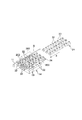
上記圧着位置Bで電子部品202に回路基板203が圧着された液晶パネル200は搬送アーム体24によって搬出される。この搬送アーム体24はX、Z及びθ方向に駆動可能となっている。すなわち、図3に示すように上記ベース15の上面にはX可動体25が設けられている。このX可動体25は上記ベース15のX方向の一端に設けられたX駆動源26によって図中矢印で示すX方向に駆動されるようになっている。
The
上記X可動体25にはθ可動体27が設けられ、上記X可動体25に設けられたθ駆動源28によって水平面に直交する軸線を中心にして回転方向に駆動可能となっている。このθ可動体27の上面にはZ駆動源29によってZ方向である上下方向に駆動される取り付け部材30が一端部をX方向に突出させて設けられている。この取り付け部材30のX方向に突出した端部には上記搬送アーム体24が取り付けられている。
The X
上記搬送アーム体24は固定部材31を有し、この固定部材31に3本のアーム32が所定間隔で一端を固定して櫛刃状に設けられている。各アーム32の上面には複数の吸着パッド33が突設されている。搬送アーム体24の吸着パッド33は、搬送ステージ14に設けられた吸着パッド22よりも高さ寸法が低くなっている。
The
上記搬送アーム体24の各アーム32はX方向に沿うとともに、先端を圧着位置Bの方向に向けて設けられている。そして、液晶パネル200を保持した搬送ステージ14が圧着位置Bで位置決めされているときに、搬送アーム体24がX方向の前進方向に駆動されて圧着位置Bに到達すると、そのアーム32は搬送ステージ14の吸着パッド22に保持された液晶パネル200の下面側に入り込むようになっている。
Each
つぎに、上記構成の圧着装置によって液晶パネル200の電子部品202に回路基板203を圧着する手順を図1、図4及び図5を参照しながら説明する。バックアップツール11には、図示せぬ搬送手段によって図1と図4に示すように回路基板203が供給される。この回路基板203には、一端部の上面に異方性導電部材204が貼着されていて、その一端部が上記バックアップツール11上に位置決め載置される。そして、その状態で上記搬送手段によって保持される。
Next, a procedure for crimping the
つぎに、予め電子部品202の一端部が圧着された液晶パネル200を保持した搬送ステージ14が図1に実線で示す位置から圧着位置Bに向かうY方向に前進駆動される。それによって、図4に示すように上記液晶パネル200に一端部が予め接続された電子部品202の他端部がバックアップツール11の上端面に位置決めされた回路基板203の一端部の上方に位置決めされる。
Next, the
電子部品202がバックアップツール11の上方に位置決めされると、上記搬送ステージ14がZ方向下方に駆動され、電子部品202の一端部が回路基板203の異方性導電部材204が貼着された一端部の上面に接触する。その状態で、加圧ツール13が下降方向に駆動され、上記電子部品202が回路基板203に圧着される。
When the
上記加圧ツール13の圧着が開始されると、搬送アーム体24は図4に鎖線で示す位置から実線で示すように圧着位置Bに向かう図中矢印で示すX方向に前進駆動され、そのアーム32が搬送ステージ14の吸着パッド22によって支持された液晶パネル200の下面側に入り込む。
When the pressurization of the pressurizing tool 13 is started, the
ついで、上記搬送アーム体24がZ方向に上昇してそのアーム32に設けられた吸着パッド33で液晶パネル200を保持したならば、搬送ステージ14の吸着パッド22による液晶パネル200の吸着状態が解除されてこの搬送ステージ14がZ方向下方に駆動される。それによって、液晶パネル200は搬送ステージ14から搬送アーム体24に受け渡される。
Next, if the
液晶パネル200の受け渡しが終了すると、搬送ステージ14は図1に示すように圧着位置Bから離れるY方向の後退方向と、必要に応じてX方向の後退方向に駆動され、図示しない液晶パネルの供給部に位置決めされる。そこで、新たな液晶パネル200が供給される。
When the delivery of the
上記供給部で新たな液晶パネル200が供給された搬送ステージ14はバックアップツール11と対向する位置に戻り、圧着位置Bで行われている液晶パネル200の電子部品202と回路基板203との圧着作業が終わるまで待機する。
The
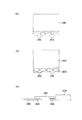
圧着作業が終了すると、加圧ツール13が上昇してから搬送アーム体24が上昇し、バックアップツール11の上端面から回路基板203を浮上させる。ついで、搬送アーム体24は図5に示すように鎖線の位置から実線で示すように、圧着位置Bから離れる図中Xで示すX方向の後退方向、つまり次工程への受け渡し位置Cに移動する。ここで、搬送アーム体24は必要に応じて図中矢印θで示すように水平方向に90度回転駆動される。それによって、搬送アーム体24は液晶パネル200の回路基板203が圧着された辺の向きを90度変え、その液晶パネル200を次工程の図示しない搬送ステージに受け渡すことができる。
When the crimping operation is completed, the
一方、上記搬送アーム体24が圧着位置Bから液晶パネル200を搬出すると、新たな液晶パネル200が供給された状態で待機していた搬送ステージ14が搬送アーム体24による搬出方向と直交するY方向の前進方向に駆動されて圧着位置Bに位置決めされる。そして、液晶パネル200に接続された電子部品203を、バックアップツール11上に位置決め保持された回路基板203に対して位置決めし、上述した圧着作業が繰り返して行われる。
On the other hand, when the
このように、この発明の圧着装置によれば、液晶パネル200を搬送ステージ14によって圧着位置Bに供給位置決めし、電子部品202に回路基板203を圧着している間に、上記液晶パネル200を搬送アーム体24に受け渡す。そして、圧着作業が終了したならば、液晶パネル200を圧着位置から搬送アーム体24によって上記搬送ステージ14による液晶パネル200の供給方向であるY方向と直交するX方向に搬出するようにした。
Thus, according to the pressure bonding apparatus of the present invention, the
そのため、上記搬送アーム体24によって圧着位置Bから液晶パネル200を搬出すると同時に、その圧着位置Bにつぎの液晶パネル200を搬送ステージ14によって供給して圧着作業を開始することが可能となる。
Therefore, the
つまり、従来のように圧着作業が終了したならば、その液晶パネル200を搬送アーム体110に受け渡すという受け渡し作業を行わずにすみ、圧着作業が終了したならば搬送アーム体24によって直接搬出することができるから、その分、サイクルタイムを短縮し、生産性を向上させることが可能となる。
That is, when the crimping operation is completed as in the prior art, it is not necessary to perform the delivery operation of delivering the
また、回路基板203が一辺に圧着された液晶パネル200の向きを、搬送アーム体24によって90度変えることができる。そのため、複数の圧着装置を並設して設け、液晶パネル200の複数の辺に回路基板203を順次圧着する場合、上記液晶パネル200の回路基板203が圧着されていない辺を順次バックアップツール11と平行になるようX方向に沿わせ、その辺に回路基板203を圧着することができる。
In addition, the orientation of the
また、液晶パネル200を持ち替える回数が2回から1回になるので、持ち替え時に液晶パネル200に与える、たとえば吸着パッドによるダメージを低減することができるから、液晶パネル200の品質低下を防止できる。
Further, since the number of times of changing the
上記一実施の形態では液晶パネルに設けられた電子部品に回路基板を圧着する例を挙げて説明したが、液晶パネルに代わりプラズマディスプレイパネルなどの他の表示パネルに電子部品を介して接続する場合などであっても、この発明を適用することができる。 Connection In the above embodiment has been described by way of example crimping the circuit board to the electronic components provided in the liquid crystal panel, via the alternative plasma display with a display on the electronic components panels such as the panel on the LCD panel The present invention can be applied even in the case of doing so.
また、圧着時に液晶パネルを搬送ステージから搬送アーム体に受け渡したならば、この搬送ステージを下降させてからX方向に後退させるようにしたが、下降後、Y方向に後退させるようにしても差し支えない。 Also, if the liquid crystal panel is transferred from the transfer stage to the transfer arm body at the time of crimping, the transfer stage is lowered and then retracted in the X direction. Absent.
11…バックアップツール、13…加圧ツール、14…搬送ステージ、24…搬送アーム体、22,33…吸着パッド、32…アーム。
DESCRIPTION OF
Claims (5)
予め上記圧着位置に位置決めされた上記回路基板に対し上記表示パネルに接続された電子部品を搬送位置決めする搬送ステージと、
この搬送ステージによって搬送された電子部品と上記回路基板を圧着する圧着手段と、
上記回路基板と電子部品を圧着している間に上記搬送ステージによって支持された上記表示パネルを受けて上記搬送ステージを退避可能とするとともに、上記圧着が終了したならば回路基板と表示パネルとを圧着位置から搬出して上記搬送ステージを圧着位置に移動可能にする搬送アーム体と
を具備したことを特徴とする部品の圧着装置。 A component crimping apparatus that positions a circuit board and an electronic component connected to a display panel at a crimping position, and crimps the circuit board and the electronic component ,
A transport stage for transporting and positioning an electronic component connected to the display panel with respect to the circuit board previously positioned at the pressure-bonding position;
Crimping means for crimping the electronic component transported by the transport stage and the circuit board ;
While receiving the display panel supported by the transfer stage while crimping the circuit board and the electronic component , the transfer stage can be retracted, and when the crimping is completed, the circuit board and the display panel are moved. A component crimping apparatus, comprising: a transport arm body that is unloaded from the crimping position and moves the transport stage to the crimping position.
予め上記圧着位置に位置決めされた上記回路基板に対し上記表示パネルに接続された電子部品を搬送ステージによって搬送して位置決めする工程と、
圧着位置に搬送された表示パネルを上記搬送ステージによって支持しこの表示パネルに接続された電子部品と上記回路基板を圧着する工程と、
上記回路基板と電子部品を圧着している間に上記搬送ステージによって支持された上記表示パネルを搬送アーム体で受けて上記搬送ステージを退避させ、この搬送ステージに新たな表示パネルを供給する工程と、
上記圧着が終了したならば圧着された回路基板と表示パネルとを上記搬送アーム体によって上記圧着位置から搬出すると同時に、新たな表示パネルが供給された上記搬送ステージを圧着位置に移動させる工程と
を具備したことを特徴とする部品の圧着方法。 Positioning the circuit board and the electronic component connected to the display panel at the crimping position, and a crimping method of the component for crimping the circuit board and the electronic component ,
A step of transporting and positioning an electronic component connected to the display panel with respect to the circuit board previously positioned at the crimping position by a transport stage;
A step of supporting the display panel transported to the crimping position by the transport stage and crimping the electronic component connected to the display panel and the circuit board ;
Receiving the display panel supported by the transfer stage while the circuit board and the electronic component are being crimped by a transfer arm body, retracting the transfer stage, and supplying a new display panel to the transfer stage; ,
When the crimping is finished, the crimped circuit board and the display panel are unloaded from the crimping position by the transport arm body, and at the same time, the transport stage supplied with a new display panel is moved to the crimping position. A method for crimping a component, comprising:
Priority Applications (1)
| Application Number | Priority Date | Filing Date | Title |
|---|---|---|---|
| JP2004364745A JP4579670B2 (en) | 2004-12-16 | 2004-12-16 | Parts crimping apparatus and crimping method |
Applications Claiming Priority (1)
| Application Number | Priority Date | Filing Date | Title |
|---|---|---|---|
| JP2004364745A JP4579670B2 (en) | 2004-12-16 | 2004-12-16 | Parts crimping apparatus and crimping method |
Publications (3)
| Publication Number | Publication Date |
|---|---|
| JP2006173396A JP2006173396A (en) | 2006-06-29 |
| JP2006173396A5 JP2006173396A5 (en) | 2009-12-03 |
| JP4579670B2 true JP4579670B2 (en) | 2010-11-10 |
Family
ID=36673803
Family Applications (1)
| Application Number | Title | Priority Date | Filing Date |
|---|---|---|---|
| JP2004364745A Active JP4579670B2 (en) | 2004-12-16 | 2004-12-16 | Parts crimping apparatus and crimping method |
Country Status (1)
| Country | Link |
|---|---|
| JP (1) | JP4579670B2 (en) |
Families Citing this family (1)
| Publication number | Priority date | Publication date | Assignee | Title |
|---|---|---|---|---|
| JP5265099B2 (en) * | 2006-09-11 | 2013-08-14 | オリンパス株式会社 | Board inspection equipment |
Citations (1)
| Publication number | Priority date | Publication date | Assignee | Title |
|---|---|---|---|---|
| JP2002057494A (en) * | 2000-08-11 | 2002-02-22 | Shibaura Mechatronics Corp | Component mounter and mounting method |
-
2004
- 2004-12-16 JP JP2004364745A patent/JP4579670B2/en active Active
Patent Citations (1)
| Publication number | Priority date | Publication date | Assignee | Title |
|---|---|---|---|---|
| JP2002057494A (en) * | 2000-08-11 | 2002-02-22 | Shibaura Mechatronics Corp | Component mounter and mounting method |
Also Published As
| Publication number | Publication date |
|---|---|
| JP2006173396A (en) | 2006-06-29 |
Similar Documents
| Publication | Publication Date | Title |
|---|---|---|
| JP4802003B2 (en) | Electronic component mounting apparatus and mounting method | |
| JPH1056259A (en) | Electronic device mounting method | |
| JP2007294826A (en) | Device and method for thermal crimping component | |
| CN106455473B (en) | Tray conveying device and mounting device | |
| JP2007311774A (en) | Different kind adhesive tape sticking method, bonding method using the same, and devices for these | |
| JP4579670B2 (en) | Parts crimping apparatus and crimping method | |
| WO2006061933A1 (en) | Component assembling device and assembling method | |
| JP2006135082A (en) | Electronic component mounting apparatus and method therefor | |
| JP4295713B2 (en) | Display device assembly apparatus and display device assembly method | |
| JP5026220B2 (en) | Component mounting method and apparatus | |
| JPWO2013141388A1 (en) | Electronic component mounting apparatus and mounting method | |
| JP7122606B2 (en) | Thermocompression bonding apparatus and thermocompression bonding method | |
| JP7122607B2 (en) | Thermocompression bonding apparatus and thermocompression bonding method | |
| CN109491111B (en) | Component mounting device and method for manufacturing mounting substrate | |
| JP6184624B1 (en) | Material pasting device | |
| JP2009099832A (en) | Component mounting device and method | |
| JP2012164706A (en) | Mounting device and mounting method of mounted member | |
| JP2009010123A (en) | Apparatus for mounting electronic component and method of manufacturing electronic component | |
| JP2008182041A (en) | Mounting device | |
| JP4537943B2 (en) | Display device assembling apparatus and assembling method | |
| JP4626278B2 (en) | Workpiece assembly device | |
| JP4579658B2 (en) | Mounting device and mounting method for mounted member | |
| JP2012123134A (en) | Fpd module assembly device | |
| KR20130004010A (en) | Module bonding method and apparatus for producing a plate type display | |
| JP7023700B2 (en) | Mounting device and mounting method |
Legal Events
| Date | Code | Title | Description |
|---|---|---|---|
| A621 | Written request for application examination |
Free format text: JAPANESE INTERMEDIATE CODE: A621 Effective date: 20071207 |
|
| A977 | Report on retrieval |
Free format text: JAPANESE INTERMEDIATE CODE: A971007 Effective date: 20090918 |
|
| A521 | Written amendment |
Free format text: JAPANESE INTERMEDIATE CODE: A523 Effective date: 20091015 |
|
| A131 | Notification of reasons for refusal |
Free format text: JAPANESE INTERMEDIATE CODE: A131 Effective date: 20100622 |
|
| A521 | Written amendment |
Free format text: JAPANESE INTERMEDIATE CODE: A523 Effective date: 20100804 |
|
| TRDD | Decision of grant or rejection written | ||
| A01 | Written decision to grant a patent or to grant a registration (utility model) |
Free format text: JAPANESE INTERMEDIATE CODE: A01 Effective date: 20100824 |
|
| A01 | Written decision to grant a patent or to grant a registration (utility model) |
Free format text: JAPANESE INTERMEDIATE CODE: A01 |
|
| A61 | First payment of annual fees (during grant procedure) |
Free format text: JAPANESE INTERMEDIATE CODE: A61 Effective date: 20100826 |
|
| FPAY | Renewal fee payment (event date is renewal date of database) |
Free format text: PAYMENT UNTIL: 20130903 Year of fee payment: 3 |
|
| R150 | Certificate of patent or registration of utility model |
Ref document number: 4579670 Country of ref document: JP Free format text: JAPANESE INTERMEDIATE CODE: R150 Free format text: JAPANESE INTERMEDIATE CODE: R150 |