JP4577891B2 - Optical recording medium - Google Patents
Optical recording medium Download PDFInfo
- Publication number
- JP4577891B2 JP4577891B2 JP2005071254A JP2005071254A JP4577891B2 JP 4577891 B2 JP4577891 B2 JP 4577891B2 JP 2005071254 A JP2005071254 A JP 2005071254A JP 2005071254 A JP2005071254 A JP 2005071254A JP 4577891 B2 JP4577891 B2 JP 4577891B2
- Authority
- JP
- Japan
- Prior art keywords
- recording
- layer
- protective layer
- atomic
- recording medium
- Prior art date
- Legal status (The legal status is an assumption and is not a legal conclusion. Google has not performed a legal analysis and makes no representation as to the accuracy of the status listed.)
- Expired - Fee Related
Links
Images


Classifications
-
- G—PHYSICS
- G11—INFORMATION STORAGE
- G11B—INFORMATION STORAGE BASED ON RELATIVE MOVEMENT BETWEEN RECORD CARRIER AND TRANSDUCER
- G11B7/00—Recording or reproducing by optical means, e.g. recording using a thermal beam of optical radiation by modifying optical properties or the physical structure, reproducing using an optical beam at lower power by sensing optical properties; Record carriers therefor
- G11B7/24—Record carriers characterised by shape, structure or physical properties, or by the selection of the material
- G11B7/241—Record carriers characterised by shape, structure or physical properties, or by the selection of the material characterised by the selection of the material
- G11B7/252—Record carriers characterised by shape, structure or physical properties, or by the selection of the material characterised by the selection of the material of layers other than recording layers
- G11B7/257—Record carriers characterised by shape, structure or physical properties, or by the selection of the material characterised by the selection of the material of layers other than recording layers of layers having properties involved in recording or reproduction, e.g. optical interference layers or sensitising layers or dielectric layers, which are protecting the recording layers
- G11B7/2578—Record carriers characterised by shape, structure or physical properties, or by the selection of the material characterised by the selection of the material of layers other than recording layers of layers having properties involved in recording or reproduction, e.g. optical interference layers or sensitising layers or dielectric layers, which are protecting the recording layers consisting essentially of inorganic materials
-
- G—PHYSICS
- G11—INFORMATION STORAGE
- G11B—INFORMATION STORAGE BASED ON RELATIVE MOVEMENT BETWEEN RECORD CARRIER AND TRANSDUCER
- G11B7/00—Recording or reproducing by optical means, e.g. recording using a thermal beam of optical radiation by modifying optical properties or the physical structure, reproducing using an optical beam at lower power by sensing optical properties; Record carriers therefor
- G11B7/004—Recording, reproducing or erasing methods; Read, write or erase circuits therefor
- G11B7/0045—Recording
- G11B7/00454—Recording involving phase-change effects
-
- G—PHYSICS
- G11—INFORMATION STORAGE
- G11B—INFORMATION STORAGE BASED ON RELATIVE MOVEMENT BETWEEN RECORD CARRIER AND TRANSDUCER
- G11B7/00—Recording or reproducing by optical means, e.g. recording using a thermal beam of optical radiation by modifying optical properties or the physical structure, reproducing using an optical beam at lower power by sensing optical properties; Record carriers therefor
- G11B7/24—Record carriers characterised by shape, structure or physical properties, or by the selection of the material
- G11B7/2407—Tracks or pits; Shape, structure or physical properties thereof
- G11B7/24085—Pits
- G11B7/24088—Pits for storing more than two values, i.e. multi-valued recording for data or prepits
-
- G—PHYSICS
- G11—INFORMATION STORAGE
- G11B—INFORMATION STORAGE BASED ON RELATIVE MOVEMENT BETWEEN RECORD CARRIER AND TRANSDUCER
- G11B7/00—Recording or reproducing by optical means, e.g. recording using a thermal beam of optical radiation by modifying optical properties or the physical structure, reproducing using an optical beam at lower power by sensing optical properties; Record carriers therefor
- G11B7/24—Record carriers characterised by shape, structure or physical properties, or by the selection of the material
- G11B7/241—Record carriers characterised by shape, structure or physical properties, or by the selection of the material characterised by the selection of the material
- G11B7/242—Record carriers characterised by shape, structure or physical properties, or by the selection of the material characterised by the selection of the material of recording layers
- G11B7/243—Record carriers characterised by shape, structure or physical properties, or by the selection of the material characterised by the selection of the material of recording layers comprising inorganic materials only, e.g. ablative layers
- G11B7/2433—Metals or elements of groups 13, 14, 15 or 16 of the Periodic System, e.g. B, Si, Ge, As, Sb, Bi, Se or Te
-
- G—PHYSICS
- G11—INFORMATION STORAGE
- G11B—INFORMATION STORAGE BASED ON RELATIVE MOVEMENT BETWEEN RECORD CARRIER AND TRANSDUCER
- G11B7/00—Recording or reproducing by optical means, e.g. recording using a thermal beam of optical radiation by modifying optical properties or the physical structure, reproducing using an optical beam at lower power by sensing optical properties; Record carriers therefor
- G11B7/24—Record carriers characterised by shape, structure or physical properties, or by the selection of the material
- G11B7/241—Record carriers characterised by shape, structure or physical properties, or by the selection of the material characterised by the selection of the material
- G11B7/242—Record carriers characterised by shape, structure or physical properties, or by the selection of the material characterised by the selection of the material of recording layers
- G11B7/243—Record carriers characterised by shape, structure or physical properties, or by the selection of the material characterised by the selection of the material of recording layers comprising inorganic materials only, e.g. ablative layers
- G11B2007/24302—Metals or metalloids
- G11B2007/24306—Metals or metalloids transition metal elements of groups 3-10
-
- G—PHYSICS
- G11—INFORMATION STORAGE
- G11B—INFORMATION STORAGE BASED ON RELATIVE MOVEMENT BETWEEN RECORD CARRIER AND TRANSDUCER
- G11B7/00—Recording or reproducing by optical means, e.g. recording using a thermal beam of optical radiation by modifying optical properties or the physical structure, reproducing using an optical beam at lower power by sensing optical properties; Record carriers therefor
- G11B7/24—Record carriers characterised by shape, structure or physical properties, or by the selection of the material
- G11B7/241—Record carriers characterised by shape, structure or physical properties, or by the selection of the material characterised by the selection of the material
- G11B7/242—Record carriers characterised by shape, structure or physical properties, or by the selection of the material characterised by the selection of the material of recording layers
- G11B7/243—Record carriers characterised by shape, structure or physical properties, or by the selection of the material characterised by the selection of the material of recording layers comprising inorganic materials only, e.g. ablative layers
- G11B2007/24302—Metals or metalloids
- G11B2007/24308—Metals or metalloids transition metal elements of group 11 (Cu, Ag, Au)
-
- G—PHYSICS
- G11—INFORMATION STORAGE
- G11B—INFORMATION STORAGE BASED ON RELATIVE MOVEMENT BETWEEN RECORD CARRIER AND TRANSDUCER
- G11B7/00—Recording or reproducing by optical means, e.g. recording using a thermal beam of optical radiation by modifying optical properties or the physical structure, reproducing using an optical beam at lower power by sensing optical properties; Record carriers therefor
- G11B7/24—Record carriers characterised by shape, structure or physical properties, or by the selection of the material
- G11B7/241—Record carriers characterised by shape, structure or physical properties, or by the selection of the material characterised by the selection of the material
- G11B7/242—Record carriers characterised by shape, structure or physical properties, or by the selection of the material characterised by the selection of the material of recording layers
- G11B7/243—Record carriers characterised by shape, structure or physical properties, or by the selection of the material characterised by the selection of the material of recording layers comprising inorganic materials only, e.g. ablative layers
- G11B2007/24302—Metals or metalloids
- G11B2007/2431—Metals or metalloids group 13 elements (B, Al, Ga, In)
-
- G—PHYSICS
- G11—INFORMATION STORAGE
- G11B—INFORMATION STORAGE BASED ON RELATIVE MOVEMENT BETWEEN RECORD CARRIER AND TRANSDUCER
- G11B7/00—Recording or reproducing by optical means, e.g. recording using a thermal beam of optical radiation by modifying optical properties or the physical structure, reproducing using an optical beam at lower power by sensing optical properties; Record carriers therefor
- G11B7/24—Record carriers characterised by shape, structure or physical properties, or by the selection of the material
- G11B7/241—Record carriers characterised by shape, structure or physical properties, or by the selection of the material characterised by the selection of the material
- G11B7/242—Record carriers characterised by shape, structure or physical properties, or by the selection of the material characterised by the selection of the material of recording layers
- G11B7/243—Record carriers characterised by shape, structure or physical properties, or by the selection of the material characterised by the selection of the material of recording layers comprising inorganic materials only, e.g. ablative layers
- G11B2007/24302—Metals or metalloids
- G11B2007/24312—Metals or metalloids group 14 elements (e.g. Si, Ge, Sn)
-
- G—PHYSICS
- G11—INFORMATION STORAGE
- G11B—INFORMATION STORAGE BASED ON RELATIVE MOVEMENT BETWEEN RECORD CARRIER AND TRANSDUCER
- G11B7/00—Recording or reproducing by optical means, e.g. recording using a thermal beam of optical radiation by modifying optical properties or the physical structure, reproducing using an optical beam at lower power by sensing optical properties; Record carriers therefor
- G11B7/24—Record carriers characterised by shape, structure or physical properties, or by the selection of the material
- G11B7/241—Record carriers characterised by shape, structure or physical properties, or by the selection of the material characterised by the selection of the material
- G11B7/242—Record carriers characterised by shape, structure or physical properties, or by the selection of the material characterised by the selection of the material of recording layers
- G11B7/243—Record carriers characterised by shape, structure or physical properties, or by the selection of the material characterised by the selection of the material of recording layers comprising inorganic materials only, e.g. ablative layers
- G11B2007/24302—Metals or metalloids
- G11B2007/24314—Metals or metalloids group 15 elements (e.g. Sb, Bi)
-
- G—PHYSICS
- G11—INFORMATION STORAGE
- G11B—INFORMATION STORAGE BASED ON RELATIVE MOVEMENT BETWEEN RECORD CARRIER AND TRANSDUCER
- G11B7/00—Recording or reproducing by optical means, e.g. recording using a thermal beam of optical radiation by modifying optical properties or the physical structure, reproducing using an optical beam at lower power by sensing optical properties; Record carriers therefor
- G11B7/24—Record carriers characterised by shape, structure or physical properties, or by the selection of the material
- G11B7/241—Record carriers characterised by shape, structure or physical properties, or by the selection of the material characterised by the selection of the material
- G11B7/242—Record carriers characterised by shape, structure or physical properties, or by the selection of the material characterised by the selection of the material of recording layers
- G11B7/243—Record carriers characterised by shape, structure or physical properties, or by the selection of the material characterised by the selection of the material of recording layers comprising inorganic materials only, e.g. ablative layers
- G11B2007/24302—Metals or metalloids
- G11B2007/24316—Metals or metalloids group 16 elements (i.e. chalcogenides, Se, Te)
-
- G—PHYSICS
- G11—INFORMATION STORAGE
- G11B—INFORMATION STORAGE BASED ON RELATIVE MOVEMENT BETWEEN RECORD CARRIER AND TRANSDUCER
- G11B7/00—Recording or reproducing by optical means, e.g. recording using a thermal beam of optical radiation by modifying optical properties or the physical structure, reproducing using an optical beam at lower power by sensing optical properties; Record carriers therefor
- G11B7/24—Record carriers characterised by shape, structure or physical properties, or by the selection of the material
- G11B7/241—Record carriers characterised by shape, structure or physical properties, or by the selection of the material characterised by the selection of the material
- G11B7/252—Record carriers characterised by shape, structure or physical properties, or by the selection of the material characterised by the selection of the material of layers other than recording layers
- G11B7/257—Record carriers characterised by shape, structure or physical properties, or by the selection of the material characterised by the selection of the material of layers other than recording layers of layers having properties involved in recording or reproduction, e.g. optical interference layers or sensitising layers or dielectric layers, which are protecting the recording layers
- G11B2007/25705—Record carriers characterised by shape, structure or physical properties, or by the selection of the material characterised by the selection of the material of layers other than recording layers of layers having properties involved in recording or reproduction, e.g. optical interference layers or sensitising layers or dielectric layers, which are protecting the recording layers consisting essentially of inorganic materials
- G11B2007/25706—Record carriers characterised by shape, structure or physical properties, or by the selection of the material characterised by the selection of the material of layers other than recording layers of layers having properties involved in recording or reproduction, e.g. optical interference layers or sensitising layers or dielectric layers, which are protecting the recording layers consisting essentially of inorganic materials containing transition metal elements (Zn, Fe, Co, Ni, Pt)
-
- G—PHYSICS
- G11—INFORMATION STORAGE
- G11B—INFORMATION STORAGE BASED ON RELATIVE MOVEMENT BETWEEN RECORD CARRIER AND TRANSDUCER
- G11B7/00—Recording or reproducing by optical means, e.g. recording using a thermal beam of optical radiation by modifying optical properties or the physical structure, reproducing using an optical beam at lower power by sensing optical properties; Record carriers therefor
- G11B7/24—Record carriers characterised by shape, structure or physical properties, or by the selection of the material
- G11B7/241—Record carriers characterised by shape, structure or physical properties, or by the selection of the material characterised by the selection of the material
- G11B7/252—Record carriers characterised by shape, structure or physical properties, or by the selection of the material characterised by the selection of the material of layers other than recording layers
- G11B7/257—Record carriers characterised by shape, structure or physical properties, or by the selection of the material characterised by the selection of the material of layers other than recording layers of layers having properties involved in recording or reproduction, e.g. optical interference layers or sensitising layers or dielectric layers, which are protecting the recording layers
- G11B2007/25705—Record carriers characterised by shape, structure or physical properties, or by the selection of the material characterised by the selection of the material of layers other than recording layers of layers having properties involved in recording or reproduction, e.g. optical interference layers or sensitising layers or dielectric layers, which are protecting the recording layers consisting essentially of inorganic materials
- G11B2007/25708—Record carriers characterised by shape, structure or physical properties, or by the selection of the material characterised by the selection of the material of layers other than recording layers of layers having properties involved in recording or reproduction, e.g. optical interference layers or sensitising layers or dielectric layers, which are protecting the recording layers consisting essentially of inorganic materials containing group 13 elements (B, Al, Ga)
-
- G—PHYSICS
- G11—INFORMATION STORAGE
- G11B—INFORMATION STORAGE BASED ON RELATIVE MOVEMENT BETWEEN RECORD CARRIER AND TRANSDUCER
- G11B7/00—Recording or reproducing by optical means, e.g. recording using a thermal beam of optical radiation by modifying optical properties or the physical structure, reproducing using an optical beam at lower power by sensing optical properties; Record carriers therefor
- G11B7/24—Record carriers characterised by shape, structure or physical properties, or by the selection of the material
- G11B7/241—Record carriers characterised by shape, structure or physical properties, or by the selection of the material characterised by the selection of the material
- G11B7/252—Record carriers characterised by shape, structure or physical properties, or by the selection of the material characterised by the selection of the material of layers other than recording layers
- G11B7/257—Record carriers characterised by shape, structure or physical properties, or by the selection of the material characterised by the selection of the material of layers other than recording layers of layers having properties involved in recording or reproduction, e.g. optical interference layers or sensitising layers or dielectric layers, which are protecting the recording layers
- G11B2007/25705—Record carriers characterised by shape, structure or physical properties, or by the selection of the material characterised by the selection of the material of layers other than recording layers of layers having properties involved in recording or reproduction, e.g. optical interference layers or sensitising layers or dielectric layers, which are protecting the recording layers consisting essentially of inorganic materials
- G11B2007/2571—Record carriers characterised by shape, structure or physical properties, or by the selection of the material characterised by the selection of the material of layers other than recording layers of layers having properties involved in recording or reproduction, e.g. optical interference layers or sensitising layers or dielectric layers, which are protecting the recording layers consisting essentially of inorganic materials containing group 14 elements except carbon (Si, Ge, Sn, Pb)
-
- G—PHYSICS
- G11—INFORMATION STORAGE
- G11B—INFORMATION STORAGE BASED ON RELATIVE MOVEMENT BETWEEN RECORD CARRIER AND TRANSDUCER
- G11B7/00—Recording or reproducing by optical means, e.g. recording using a thermal beam of optical radiation by modifying optical properties or the physical structure, reproducing using an optical beam at lower power by sensing optical properties; Record carriers therefor
- G11B7/24—Record carriers characterised by shape, structure or physical properties, or by the selection of the material
- G11B7/241—Record carriers characterised by shape, structure or physical properties, or by the selection of the material characterised by the selection of the material
- G11B7/252—Record carriers characterised by shape, structure or physical properties, or by the selection of the material characterised by the selection of the material of layers other than recording layers
- G11B7/257—Record carriers characterised by shape, structure or physical properties, or by the selection of the material characterised by the selection of the material of layers other than recording layers of layers having properties involved in recording or reproduction, e.g. optical interference layers or sensitising layers or dielectric layers, which are protecting the recording layers
- G11B2007/25705—Record carriers characterised by shape, structure or physical properties, or by the selection of the material characterised by the selection of the material of layers other than recording layers of layers having properties involved in recording or reproduction, e.g. optical interference layers or sensitising layers or dielectric layers, which are protecting the recording layers consisting essentially of inorganic materials
- G11B2007/25711—Record carriers characterised by shape, structure or physical properties, or by the selection of the material characterised by the selection of the material of layers other than recording layers of layers having properties involved in recording or reproduction, e.g. optical interference layers or sensitising layers or dielectric layers, which are protecting the recording layers consisting essentially of inorganic materials containing carbon
-
- G—PHYSICS
- G11—INFORMATION STORAGE
- G11B—INFORMATION STORAGE BASED ON RELATIVE MOVEMENT BETWEEN RECORD CARRIER AND TRANSDUCER
- G11B7/00—Recording or reproducing by optical means, e.g. recording using a thermal beam of optical radiation by modifying optical properties or the physical structure, reproducing using an optical beam at lower power by sensing optical properties; Record carriers therefor
- G11B7/24—Record carriers characterised by shape, structure or physical properties, or by the selection of the material
- G11B7/241—Record carriers characterised by shape, structure or physical properties, or by the selection of the material characterised by the selection of the material
- G11B7/252—Record carriers characterised by shape, structure or physical properties, or by the selection of the material characterised by the selection of the material of layers other than recording layers
- G11B7/257—Record carriers characterised by shape, structure or physical properties, or by the selection of the material characterised by the selection of the material of layers other than recording layers of layers having properties involved in recording or reproduction, e.g. optical interference layers or sensitising layers or dielectric layers, which are protecting the recording layers
- G11B2007/25705—Record carriers characterised by shape, structure or physical properties, or by the selection of the material characterised by the selection of the material of layers other than recording layers of layers having properties involved in recording or reproduction, e.g. optical interference layers or sensitising layers or dielectric layers, which are protecting the recording layers consisting essentially of inorganic materials
- G11B2007/25713—Record carriers characterised by shape, structure or physical properties, or by the selection of the material characterised by the selection of the material of layers other than recording layers of layers having properties involved in recording or reproduction, e.g. optical interference layers or sensitising layers or dielectric layers, which are protecting the recording layers consisting essentially of inorganic materials containing nitrogen
-
- G—PHYSICS
- G11—INFORMATION STORAGE
- G11B—INFORMATION STORAGE BASED ON RELATIVE MOVEMENT BETWEEN RECORD CARRIER AND TRANSDUCER
- G11B7/00—Recording or reproducing by optical means, e.g. recording using a thermal beam of optical radiation by modifying optical properties or the physical structure, reproducing using an optical beam at lower power by sensing optical properties; Record carriers therefor
- G11B7/24—Record carriers characterised by shape, structure or physical properties, or by the selection of the material
- G11B7/241—Record carriers characterised by shape, structure or physical properties, or by the selection of the material characterised by the selection of the material
- G11B7/252—Record carriers characterised by shape, structure or physical properties, or by the selection of the material characterised by the selection of the material of layers other than recording layers
- G11B7/257—Record carriers characterised by shape, structure or physical properties, or by the selection of the material characterised by the selection of the material of layers other than recording layers of layers having properties involved in recording or reproduction, e.g. optical interference layers or sensitising layers or dielectric layers, which are protecting the recording layers
- G11B2007/25705—Record carriers characterised by shape, structure or physical properties, or by the selection of the material characterised by the selection of the material of layers other than recording layers of layers having properties involved in recording or reproduction, e.g. optical interference layers or sensitising layers or dielectric layers, which are protecting the recording layers consisting essentially of inorganic materials
- G11B2007/25715—Record carriers characterised by shape, structure or physical properties, or by the selection of the material characterised by the selection of the material of layers other than recording layers of layers having properties involved in recording or reproduction, e.g. optical interference layers or sensitising layers or dielectric layers, which are protecting the recording layers consisting essentially of inorganic materials containing oxygen
-
- G—PHYSICS
- G11—INFORMATION STORAGE
- G11B—INFORMATION STORAGE BASED ON RELATIVE MOVEMENT BETWEEN RECORD CARRIER AND TRANSDUCER
- G11B7/00—Recording or reproducing by optical means, e.g. recording using a thermal beam of optical radiation by modifying optical properties or the physical structure, reproducing using an optical beam at lower power by sensing optical properties; Record carriers therefor
- G11B7/24—Record carriers characterised by shape, structure or physical properties, or by the selection of the material
- G11B7/241—Record carriers characterised by shape, structure or physical properties, or by the selection of the material characterised by the selection of the material
- G11B7/252—Record carriers characterised by shape, structure or physical properties, or by the selection of the material characterised by the selection of the material of layers other than recording layers
- G11B7/257—Record carriers characterised by shape, structure or physical properties, or by the selection of the material characterised by the selection of the material of layers other than recording layers of layers having properties involved in recording or reproduction, e.g. optical interference layers or sensitising layers or dielectric layers, which are protecting the recording layers
- G11B2007/25705—Record carriers characterised by shape, structure or physical properties, or by the selection of the material characterised by the selection of the material of layers other than recording layers of layers having properties involved in recording or reproduction, e.g. optical interference layers or sensitising layers or dielectric layers, which are protecting the recording layers consisting essentially of inorganic materials
- G11B2007/25716—Record carriers characterised by shape, structure or physical properties, or by the selection of the material characterised by the selection of the material of layers other than recording layers of layers having properties involved in recording or reproduction, e.g. optical interference layers or sensitising layers or dielectric layers, which are protecting the recording layers consisting essentially of inorganic materials containing sulfur
-
- G—PHYSICS
- G11—INFORMATION STORAGE
- G11B—INFORMATION STORAGE BASED ON RELATIVE MOVEMENT BETWEEN RECORD CARRIER AND TRANSDUCER
- G11B7/00—Recording or reproducing by optical means, e.g. recording using a thermal beam of optical radiation by modifying optical properties or the physical structure, reproducing using an optical beam at lower power by sensing optical properties; Record carriers therefor
- G11B7/24—Record carriers characterised by shape, structure or physical properties, or by the selection of the material
- G11B7/241—Record carriers characterised by shape, structure or physical properties, or by the selection of the material characterised by the selection of the material
- G11B7/252—Record carriers characterised by shape, structure or physical properties, or by the selection of the material characterised by the selection of the material of layers other than recording layers
- G11B7/253—Record carriers characterised by shape, structure or physical properties, or by the selection of the material characterised by the selection of the material of layers other than recording layers of substrates
- G11B7/2533—Record carriers characterised by shape, structure or physical properties, or by the selection of the material characterised by the selection of the material of layers other than recording layers of substrates comprising resins
- G11B7/2534—Record carriers characterised by shape, structure or physical properties, or by the selection of the material characterised by the selection of the material of layers other than recording layers of substrates comprising resins polycarbonates [PC]
-
- G—PHYSICS
- G11—INFORMATION STORAGE
- G11B—INFORMATION STORAGE BASED ON RELATIVE MOVEMENT BETWEEN RECORD CARRIER AND TRANSDUCER
- G11B7/00—Recording or reproducing by optical means, e.g. recording using a thermal beam of optical radiation by modifying optical properties or the physical structure, reproducing using an optical beam at lower power by sensing optical properties; Record carriers therefor
- G11B7/24—Record carriers characterised by shape, structure or physical properties, or by the selection of the material
- G11B7/241—Record carriers characterised by shape, structure or physical properties, or by the selection of the material characterised by the selection of the material
- G11B7/252—Record carriers characterised by shape, structure or physical properties, or by the selection of the material characterised by the selection of the material of layers other than recording layers
- G11B7/256—Record carriers characterised by shape, structure or physical properties, or by the selection of the material characterised by the selection of the material of layers other than recording layers of layers improving adhesion between layers
-
- G—PHYSICS
- G11—INFORMATION STORAGE
- G11B—INFORMATION STORAGE BASED ON RELATIVE MOVEMENT BETWEEN RECORD CARRIER AND TRANSDUCER
- G11B7/00—Recording or reproducing by optical means, e.g. recording using a thermal beam of optical radiation by modifying optical properties or the physical structure, reproducing using an optical beam at lower power by sensing optical properties; Record carriers therefor
- G11B7/24—Record carriers characterised by shape, structure or physical properties, or by the selection of the material
- G11B7/241—Record carriers characterised by shape, structure or physical properties, or by the selection of the material characterised by the selection of the material
- G11B7/252—Record carriers characterised by shape, structure or physical properties, or by the selection of the material characterised by the selection of the material of layers other than recording layers
- G11B7/258—Record carriers characterised by shape, structure or physical properties, or by the selection of the material characterised by the selection of the material of layers other than recording layers of reflective layers
- G11B7/259—Record carriers characterised by shape, structure or physical properties, or by the selection of the material characterised by the selection of the material of layers other than recording layers of reflective layers based on silver
Description
本発明は、相変化型光記録媒体に関する。 The present invention relates to a phase change optical recording medium.
現在実用化されている光記録媒体として結晶状態と非晶質(アモルファス)状態の可逆的相変化を利用した、いわゆる相変化型光記録媒体がある。その記録材料としてはSb、Teを母体としAg、In、Ge等を添加したAgInSbTe系、AgInSbTeGe系材料がある。これらはCD−RW、DVD−RW、DVD+RW媒体に用いられる。これらの相変化型光記録媒体は、何れも螺旋状又は同心円状の溝を有するプラスチック基板上に、下部保護層、記録層、上部保護層、反射層を基本とする積層構造を有し、2値情報の記録・再生を行うものである。そして高密度、大容量化のため、媒体に照射する光の波長を、DVDで用いられている650〜660nmから、青紫色領域である405nmのLDに変えたり、NA0.85の高NAレンズを用いることにより、片面20GB以上の容量が可能になっている。
一方、DVDを記録再生可能とするために、NAを同じ0.65とする方式も考えられる。しかし、容量がNA0.85の場合より小さくなるため、本出願人は、アモルファス記録マークの周辺結晶部に対する占有率の違いで多値情報を記録し、記録容量20GB以上を達成する方法について既に提案している(非特許文献1、特許文献1〜2)。
There is a so-called phase change type optical recording medium that uses a reversible phase change between a crystalline state and an amorphous state as an optical recording medium that is currently in practical use. As the recording material, there are AgInSbTe-based materials and AgInSbTeGe-based materials in which Sb and Te are used as base materials and Ag, In, Ge, etc. are added. These are used for CD-RW, DVD-RW, and DVD + RW media. Each of these phase-change optical recording media has a laminated structure based on a lower protective layer, a recording layer, an upper protective layer, and a reflective layer on a plastic substrate having spiral or concentric grooves. Value information is recorded / reproduced. In order to increase the density and capacity, the wavelength of the light irradiating the medium is changed from 650 to 660 nm used in DVD to a 405 nm LD in the blue-violet region, or a high NA lens with NA 0.85 is used. By using it, a capacity of 20 GB or more on one side is possible.
On the other hand, in order to enable recording / reproduction of a DVD, a method of setting NA to the same 0.65 is also conceivable. However, since the capacity is smaller than that in the case of NA 0.85, the present applicant has already proposed a method for recording multi-value information with a difference in the occupation ratio of the amorphous recording mark with respect to the peripheral crystal part and achieving a recording capacity of 20 GB or more. (Non-Patent
この非特許文献1の技術について説明する。
図1に、マーク占有率とRf信号の概念図を示す。記録マークは各セルの略中心に位置している。記録マークが書換え可能な相変化材料の相状態或いは基板の凹凸形状として記録された位相ピットでも同じ関係となる。記録マークが基板の凹凸形状として記録された位相ピットの場合は、Rf信号の信号利得が最大となるように位相ピットの光学的溝深さをλ/4(λは記録再生レーザの波長)とする必要がある。Rf信号値は、記録再生用の集光ビームがセルの中心に位置する場合の値で与えられ、1つのセルに占める記録マークの占有率の大小によって変化する。一般的にRf信号値は、記録マークが存在しないときに最大となり、記録マークの占有率が最も高いときに最小となる。
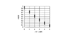
このような面積変調方式により、例えば、記録マークパタン数(多値レベル数)=6で多値記録を行うと、各記録マークパタンからのRf信号値は図2のような分布を示す。Rf信号値は、その最大値と最小値の幅(ダイナミックレンジ、DR)を1として正規化された数値で表記されている。記録再生は、λ=650nm、NA=0.65(集光ビーム径=約0.8μm)の光学系を用いて行い、セルの円周方向長さ(以下、セル長と記す)を約0.6μmとした。このような多値記録マークは、図3のような記録ストラテジで、記録パワーPw、消去パワーPe、ボトムパワーPbのパワー及びその開始時間をパラメータとしてレーザ変調することにより形成できる。
The technique of this
FIG. 1 is a conceptual diagram of mark occupancy and Rf signal. The recording mark is located at the approximate center of each cell. The same relationship applies to phase pits recorded as phase states of rewritable phase change materials or irregularities on the substrate. In the case of a phase pit in which the recording mark is recorded as an uneven shape of the substrate, the optical groove depth of the phase pit is λ / 4 (λ is the wavelength of the recording / reproducing laser) so that the signal gain of the Rf signal is maximized. There is a need to. The Rf signal value is given as a value when the recording / reproducing focused beam is located at the center of the cell, and changes depending on the occupation ratio of the recording mark in one cell. Generally, the Rf signal value becomes maximum when no recording mark exists, and becomes minimum when the occupation ratio of the recording mark is the highest.
For example, when multi-value recording is performed with the number of recording mark patterns (number of multi-value levels) = 6 by such an area modulation method, Rf signal values from the respective recording mark patterns show a distribution as shown in FIG. The Rf signal value is represented by a numerical value normalized with the width (dynamic range, DR) of the maximum value and the minimum value being 1. Recording / reproduction is performed using an optical system with λ = 650 nm and NA = 0.65 (condensed beam diameter = about 0.8 μm), and the circumferential length of the cell (hereinafter referred to as cell length) is about 0. .6 μm. Such a multi-value recording mark can be formed by laser modulation using the recording strategy as shown in FIG. 3 with the recording power Pw, the erasing power Pe, the power of the bottom power Pb, and the start time thereof as parameters.
上記のような多値記録方式においては、記録線密度を上げていく(=セル長を短くしていく)と、次第に集光ビーム径に対してセル長の方が短くなり、対象となるセルを再生するとき、集光ビームが前後のセルにはみ出すようになる。そのため対象となるセルのマーク占有率が同じでも、前後のセルのマーク占有率の組合せにより、対象となるセルから再生されるRf信号値が影響を受ける。即ち、前後のマークとの符号間干渉が起こるようになる。この影響で、図2に示すように、各パタンにおけるRf信号値は偏差を持った分布になる。即ち、対象となるセルがどの記録マークのパタンであるかを判定するためには、各記録マークから再生されるRf信号値の間隔が、前記偏差以上に離れている必要がある。図2の場合、各パターン番号の記録マークのRf信号値の間隔と偏差はほぼ同等であり、記録マークパタンの判定ができる限界になっている。 In the multi-value recording method as described above, as the recording linear density is increased (= the cell length is shortened), the cell length gradually becomes shorter than the focused beam diameter, and the target cell When reproducing the light, the focused beam protrudes to the front and rear cells. Therefore, even if the mark occupancy of the target cell is the same, the Rf signal value reproduced from the target cell is affected by the combination of the mark occupancy of the preceding and subsequent cells. That is, intersymbol interference occurs with the preceding and following marks. Due to this influence, as shown in FIG. 2, the Rf signal value in each pattern has a distribution with a deviation. That is, in order to determine which recording mark pattern the target cell has, the interval between the Rf signal values reproduced from each recording mark needs to be larger than the deviation. In the case of FIG. 2, the intervals and deviations of the Rf signal values of the recording marks of the respective pattern numbers are almost the same, which is a limit for determining the recording mark pattern.
この限界を打破する技術として提案されたのが、非特許文献1に開示された、連続する3つのデータセルを用いた多値判定技術である。この技術は、連続する3つのデータセルの組み合わせパターン(8値記録時、83=512通り)からなる多値信号分布を学習し、そのパターンテーブルを作成するステップと、未知データの再生信号結果から3連続マークパターンを予測した後、前記パターンテーブルを参照して再生対象となる未知信号を多値判定するステップとからなる。これにより、再生時に符号間干渉が生じるような従来のセル密度或いはSDR値においても、多値信号判定のエラー率を低くすることが可能になった。ここでSDR値とは、多値階調数をnとした時の各多値信号の標準偏差σiの平均値と、多値Rf信号のダイナミックレンジ(DR)との比=Σσi/(n×DR)で表され、2値記録におけるジッターに相当する信号品質である。一般に、多値階調数nを一定とすると、多値信号の標準偏差σiが小さいほど、且つダイナミックレンジ(DR)が大きいほどSDR値は小さくなり、多値信号の分別性が良くなってエラー率は低くなる。逆に、多値階調数nを大きくすると、SDR値は大きくなりエラー率は高くなる。
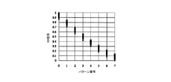
このような多値判定技術を用いると、例えば多値階調数を8に増やして、各Rf信号値の分布が重なり合ってしまう図4のような場合でも、8値の多値判定が可能となる。
A multi-value determination technique using three consecutive data cells disclosed in
When such a multi-value determination technique is used, for example, even when the number of multi-value gradations is increased to 8 and the distributions of the Rf signal values overlap each other, 8-value multi-value determination can be performed. Become.
上記多値記録方式においても、前述の相変化記録材料を用いることができる。しかし、今後は、書き換え可能或いは1回記録可能なDVD−R/RW、DVD+R/RW媒体、青色LDにより記録再生する書き換え可能な相変化媒体(Blu−ray規格)、多値記録用相変化媒体おいて高速記録再生が要求される。これを可能にするためには、相変化記録材料の結晶化速度の高速化とマークの長期保存性の両立が課題となってくる。これまで用いられてきたSb70Te30共晶組成を母体とするAgInSbTe系では限界がある。実際にDVDでは、8倍速相当乃至それ以上の記録線速ではマークの長期保存性が問題となり用いることができない。そこで、Sb、Teを母体とする材料ではなく、Sbを含む他の材料系を用いることで高速化及び保存安定性の両立が模索されている。これらの材料系としては、GaSb系、GeSb系がある。例えば特許文献3には、GeSb系にInを加えた材料が開示されており、添加元素として、Sn、Bi、Zn、Ga等を10原子%以下添加すると良いことも記載されている。このような材料としては、GaSb系、GeSb系がある。その他にGeSbSnIn系(特許文献4)、GeMnSb系(特許文献5)、GeSbSnにTe、In、Gaを添加する(特許文献6)が挙げられるが、本発明の課題を解決するに足る材料ではない。
Also in the multi-value recording method, the above-described phase change recording material can be used. However, in the future, rewritable or once recordable DVD-R / RW, DVD + R / RW media, rewritable phase change media (Blu-ray standard) for recording / reproducing with blue LD, phase change media for multi-value recording In this case, high-speed recording / reproduction is required. In order to make this possible, it is necessary to increase both the crystallization speed of the phase change recording material and the long-term storage stability of the mark. There is a limit in the AgInSbTe system based on the Sb 70 Te 30 eutectic composition used so far. Actually, DVD cannot be used at a recording linear velocity equivalent to or higher than 8 × speed because of the problem of long-term mark storability. Therefore, not only materials based on Sb and Te but also other material systems containing Sb are being sought to achieve both high speed and storage stability. These materials include GaSb and GeSb. For example,
任意の長さのマーク長を制御よく記録でき、高線速記録が可能でしかも長期保存性の優れた相変化記録材料が、今後、高速化、大容量化の要求に伴って必要になってくる。特に、大容量になればなるほど高速記録再生の要求が高くなる。非晶質相であるマークの長さが0.1μm付近で、しかもこの長さ近傍でマーク長をより制御良く記録することは、2値及び多値記録に必須である。特に、多値記録では最短マークと最長マークの長さの差が小さく、しかもその間を細かくマーク長制御しなければならない。
また、多値記録方式においては、記録される溝の中でマークの面積を変化させ、そこから再生される反射信号電圧を等間隔に分割して情報を読み取るため、高温高湿環境下でのマークの消失やマーク長の変化だけでなく、マーク間の結晶状態の変化による反射率変動があっても、再生された信号のエラーが増大し情報が読めなくなってしまう。更に、光の波長が650nmと青紫色の405nmの両方の領域において、非晶質相と結晶相の光学定数の差が大きく取れる材料であることも、2値及び多値記録に要求される。特に、多値記録は反射信号のレベルで情報を読み取るため、未記録状態である0レベルの反射率が高く、レベル間の反射信号電圧差が大きく、かつ最大レベル(例えば8値目の信号)と0レベルの信号差(いわゆる変調度)が大きいほど良い。
本発明は、これらの要求を満たす相変化記録材料及び最適な構成の相変化光記録媒体の提供を目的とする。
Phase change recording materials that can record arbitrarily long mark lengths with high controllability, are capable of high linear velocity recording, and have excellent long-term storability will become necessary in the future as demands for higher speeds and larger capacities increase. come. In particular, the higher the capacity, the higher the demand for high-speed recording / reproduction. It is indispensable for binary and multi-level recording that the mark which is an amorphous phase has a length of about 0.1 μm, and that the mark length is recorded with better control in the vicinity of this length. In particular, in multi-level recording, the difference between the lengths of the shortest mark and the longest mark is small, and the mark length must be finely controlled between them.
In the multi-value recording method, the area of the mark is changed in the groove to be recorded, and the reflected signal voltage reproduced therefrom is divided into equal intervals to read the information. Even if the reflectance fluctuates due not only to the disappearance of the mark or the change in the mark length but also due to the change in the crystal state between the marks, the error of the reproduced signal increases and the information cannot be read. Furthermore, it is also required for binary recording and multi-value recording that the material has a large difference in optical constant between the amorphous phase and the crystalline phase in both the light wavelength region of 650 nm and blue-violet 405 nm. In particular, since multilevel recording reads information at the level of the reflected signal, the reflectivity of the 0 level, which is an unrecorded state, is high, the reflected signal voltage difference between the levels is large, and the maximum level (for example, the eighth value signal). And 0 level signal difference (so-called modulation factor) is larger.
It is an object of the present invention to provide a phase change recording material that satisfies these requirements and a phase change optical recording medium having an optimum configuration.
上記課題は、次の1)〜6)の発明によって解決される。
1) 基板上に、少なくとも、下部保護層、光照射による非晶質相と結晶相の可逆的相変化に伴う光学定数の変化を利用した相変化記録層、上部保護層、反射層を有し、相変化記録層が、GeαSbβSnγMnδXε〔5≦α≦25、45≦β≦75、10≦γ≦30、0.5≦δ≦20、0≦ε≦15、α+β+γ+δ+ε=100(原子%)、XはIn、Bi、Te、Ag、Al、Zn、Co、Ni、Cuから選ばれる少なくとも一つの元素〕からなることを特徴とする光記録媒体。
2) 相変化記録層が更にGaを7原子%以下含有することを特徴とする1)記載の光記録媒体。
3) 基板上に、Ag又はAg合金反射層、下部保護層、相変化記録層、上部保護層、接着層、カバー基板をこの順に有するか、或いは、Ag又はAg合金反射層、硫化防止層、下部保護層、相変化記録層、上部保護層、接着層、カバー基板をこの順に有することを特徴とする1)又は2)記載の光記録媒体。
4) 下部保護層と相変化記録層の間に膜厚1〜10nmの界面層を有し、界面層がZrO2とY2O3とTiO2の混合物、SiO2とNb2O5の混合物、又はSiO2とTa2O5の混合物からなることを特徴とする1)〜3)の何れかに記載の光記録媒体。
5) 相変化記録層と上部保護層の間に界面層を有することを特徴とする1)〜4)の何れかに記載の光記録媒体。
6) 光入射側の保護層材料が、ZnS:SiO2=60〜85:40〜15(モル%)からなり、反射層側の保護層材料が、ZnS:SiO2=30〜85:70〜15(モル%)からなることを特徴とする1)〜5)の何れかに記載の光記録媒体。
The above problems are solved by the following inventions 1) to 6).
1) At least a lower protective layer, a phase change recording layer using an optical constant change accompanying a reversible phase change between an amorphous phase and a crystalline phase by light irradiation, an upper protective layer, and a reflective layer on a substrate , GeαSbβSnγMnδXε [5 ≦ α ≦ 25, 45 ≦ β ≦ 75, 10 ≦ γ ≦ 30, 0.5 ≦ δ ≦ 20, 0 ≦ ε ≦ 15, α + β + γ + δ + ε = 100 (atomic%), Is an at least one element selected from In, Bi, Te, Ag, Al, Zn, Co, Ni, and Cu].
2) The optical recording medium according to 1), wherein the phase change recording layer further contains 7 atomic% or less of Ga.
3) The substrate has an Ag or Ag alloy reflective layer, a lower protective layer, a phase change recording layer, an upper protective layer, an adhesive layer, and a cover substrate in this order, or an Ag or Ag alloy reflective layer, an anti-sulfurization layer, The optical recording medium according to 1) or 2), comprising a lower protective layer, a phase change recording layer, an upper protective layer, an adhesive layer, and a cover substrate in this order.
4) has a surface layer having a
5) The optical recording medium according to any one of 1) to 4), wherein an interface layer is provided between the phase change recording layer and the upper protective layer.
6) The protective layer material on the light incident side is made of ZnS: SiO 2 = 60 to 85:40 to 15 (mol%), and the protective layer material on the reflective layer side is ZnS: SiO 2 = 30 to 85:70 to The optical recording medium according to any one of 1) to 5), comprising 15 (mol%).
以下、上記本発明について詳しく説明する。
本発明の光記録媒体は2値及び多値記録が可能であるが、多値記録には、前述した非特許文献1の多値記録方法を採用することができる。
光記録媒体の構成例としては、図5に示すように、透明基板上に下部保護層、レーザー光の照射による非晶質相と結晶相の可逆的相変化に伴う光学定数の変化を利用した相変化記録層、上部保護層、反射層の順に積層したものが挙げられる。
透明基板は、レーザー光の波長帯域である少なくとも400〜800nmの範囲で透明であり、複屈折がより小さいことが望ましい。また、基板成形過程においても基板の半径位置毎に複屈折の分布を生じることがあるため、材料の複屈折がより小さく成形後の分布も小さいことが要求される。複屈折が無いということではガラス基板が好ましいが、より安価なポリカーカーボネート製基板を用いることが多い。
また、基板には、一般に、溝深さ20〜35nm、溝幅0.2〜0.3μm、溝ピッチ0.40〜0.50μmの案内溝を設ける。
Hereinafter, the present invention will be described in detail.
The optical recording medium of the present invention can perform binary and multi-value recording, and the multi-value recording method of
As an example of the configuration of the optical recording medium, as shown in FIG. 5, a lower protective layer is used on a transparent substrate, and a change in optical constant accompanying a reversible phase change between an amorphous phase and a crystalline phase due to laser light irradiation is used. Examples include a layer in which a phase change recording layer, an upper protective layer, and a reflective layer are laminated in this order.
The transparent substrate is preferably transparent in the range of at least 400 to 800 nm, which is the wavelength band of laser light, and preferably has a smaller birefringence. Also, in the substrate molding process, birefringence distribution may occur for each radial position of the substrate, so that the birefringence of the material is smaller and the distribution after molding is required to be small. A glass substrate is preferred because it has no birefringence, but a cheaper polycarbonate substrate is often used.
The substrate is generally provided with guide grooves having a groove depth of 20 to 35 nm, a groove width of 0.2 to 0.3 μm, and a groove pitch of 0.40 to 0.50 μm.
下部保護層材料としては、酸化物、窒化物、炭化物、及びこれらの混合物が挙げられるが、波長400nm付近での透過率がより高い材料が適している。SiCなどの炭化物で光吸収が大きいものは適さないが、数nmの薄い膜厚とし、酸化物、窒化物の保護層と組み合わせて光吸収機能を持たせるための層として用いることはできる。中でも、ZnSとSiO2の混合物(ZnSSiO2)であって、ZnS:SiO2=30〜90:70〜10(モル%)のものが好ましく、ZnS:SiO2=60〜85:40〜15がより好ましい。この材料を用いれば、繰り返し記録、高温環境下での膜自身の結晶化が抑制され、高い記録感度を維持でき、繰り返し記録時の膜変形も抑えられる。
また、下部保護層を2層又は多層にする場合もある。繰り返し記録を行なった場合に、記録回数が増えるにつれて、記録層と下部保護層の間で保護層を構成する元素の記録層内への拡散が起きるため、図6に示すように、下部保護層と記録層の間に界面層を設けてもよい。更に記録層と上部保護層の間にも界面層を設けることができる(図示せず)。
Examples of the lower protective layer material include oxides, nitrides, carbides, and mixtures thereof, but materials having higher transmittance near a wavelength of 400 nm are suitable. A carbide such as SiC having a large light absorption is not suitable, but it can be used as a layer having a thin film thickness of several nanometers and having a light absorption function in combination with a protective layer of oxide or nitride. Among them, a mixture of ZnS and SiO 2 (ZnSSiO 2 ), preferably ZnS: SiO 2 = 30 to 90:70 to 10 (mol%), and ZnS: SiO 2 = 60 to 85:40 to 15 is preferable. More preferred. By using this material, repeated recording and crystallization of the film itself under a high temperature environment can be suppressed, high recording sensitivity can be maintained, and film deformation during repeated recording can also be suppressed.
In some cases, the lower protective layer has two layers or multiple layers. When repeated recording is performed, as the number of times of recording increases, diffusion of elements constituting the protective layer into the recording layer occurs between the recording layer and the lower protective layer. Therefore, as shown in FIG. An interface layer may be provided between the recording layer and the recording layer. Further, an interface layer can be provided between the recording layer and the upper protective layer (not shown).
更に別の構成としては、基板上にZnSSiO2以外の酸化物、窒化物、又はそれらの混合物を用いて、その上にZnSSiO2層、記録層の順に積層する構成がある。この層構成は、繰り返し記録時のレーザー光の放熱、つまり、熱が基板に到達する前に溝周辺部に放熱させることを目的とする。また界面層を敷く場合は、繰り返し記録特性の向上以外の目的として、用いる記録層材料によって、消去特性を向上させるための結晶化促進補助層の働きを持たせることもある。この場合は界面層が結晶状態(多結晶状態)にあって、記録層の核形成・成長を助ける作用がある。材料としては酸化物、炭化物、窒化物を用いるが、高温高湿下の長期保存性(アーカイバル保存)を損なわないようにするためには、膜厚は数nmの厚さが良い。
本発明では界面層は主に繰り返し記録特性を劣化させないことを目的として用い、特に青紫色レーザーを使用し、ZnSSiO2の膜厚が30〜100nmの範囲にあるときに用いる。下部保護層と記録層の間に界面層を設けることにより、下部保護層が記録時の高温の熱により劣化し、屈折率の減少による反射率の低下及び記録特性の劣化が起こることを防止できる。
As yet another configuration, there is a configuration in which an oxide other than ZnSSiO 2 , a nitride, or a mixture thereof is used on a substrate, and a ZnSSiO 2 layer and a recording layer are stacked in that order. The purpose of this layer structure is to dissipate laser light during repeated recording, that is, to dissipate heat to the periphery of the groove before the heat reaches the substrate. When the interface layer is laid, for the purpose other than the improvement of the repetitive recording characteristics, depending on the recording layer material to be used, there may be a function of a crystallization promotion auxiliary layer for improving the erasing characteristics. In this case, the interface layer is in a crystalline state (polycrystalline state), and has an effect of assisting nucleation / growth of the recording layer. Oxides, carbides, and nitrides are used as materials. In order not to impair long-term storage under high temperature and high humidity (archival storage), the film thickness is preferably several nm.
In the present invention, the interface layer is used mainly for the purpose of not deteriorating the repetitive recording characteristics. In particular, a blue-violet laser is used, and is used when the film thickness of ZnSSiO 2 is in the range of 30 to 100 nm. By providing an interface layer between the lower protective layer and the recording layer, it is possible to prevent the lower protective layer from being deteriorated due to high-temperature heat during recording, resulting in a decrease in reflectance and a deterioration in recording characteristics due to a decrease in refractive index. .
界面層の材料としては、透明でしかも屈折率がZnSSiO2と同じ2.3前後(波長405nmにおいて)が良い。その原材料としてはSiO2、Al2O3、ZrO2、MgO、ZnO、Nb2O5、Ta2O5、Y2O3、TiO2、AlN、SiNなどが挙げられるが、融点が高く、屈折率が約2.3のZrO2とTiO2の混合物、これに更にY2O3を加えたもの、SiO2とNb2O5の混合物、SiO2とTa2O5の混合物が良い。スパッタ法で成膜する場合のターゲット材として用いるには、ZrO2にY2O3を3〜8原子%混合すれば大面積のターゲットを用いても割れないようにできる。ZrO2、Y2O3、TiO2の混合物における各酸化物の割合(モル%)は、〔(ZrO2)1−x(Y2O3)x〕1−y(TiO2)yとして、2≦x≦8、10≦y≦70の範囲が良い。In2O3とZnOの混合物やIn2O3とMgOの混合物も光透過性、放熱性の面で好ましい。
界面層の膜厚は1〜10nmが良い。1nm未満の膜を製膜することは難しく、10nmを超えると、熱伝導率が高くなって周辺に熱が広がり易くなり、記録感度が低下し記録特性が劣化する。更に、高温環境下に放置しておくと、結晶核生成・成長により記録マークが小さくなり、材料によっては消えてしまうことがある。
As the material of the interfacial layer, transparent yet refractive index (at a wavelength of 405 nm) same as 2.3 before and after the ZnSSiO 2 is good. The raw materials include SiO 2 , Al 2 O 3 , ZrO 2 , MgO, ZnO, Nb 2 O 5 , Ta 2 O 5 , Y 2 O 3 , TiO 2 , AlN, SiN, etc., but the melting point is high, A mixture of ZrO 2 and TiO 2 having a refractive index of about 2.3, a mixture obtained by further adding Y 2 O 3 , a mixture of SiO 2 and Nb 2 O 5, and a mixture of SiO 2 and Ta 2 O 5 are preferable. For use as a target material in the case of forming a film by sputtering, if ZrO 2 is mixed with 3 to 8 atomic% of Y 2 O 3 , it can be prevented from cracking even if a large area target is used. The ratio (mol%) of each oxide in the mixture of ZrO 2 , Y 2 O 3 , and TiO 2 is [(ZrO 2 ) 1−x (Y 2 O 3 ) x] 1−y (TiO 2 ) y, A range of 2 ≦ x ≦ 8 and 10 ≦ y ≦ 70 is preferable. A mixture of In 2 O 3 and ZnO or a mixture of In 2 O 3 and MgO is also preferable in terms of light transmittance and heat dissipation.
The film thickness of the interface layer is preferably 1 to 10 nm. It is difficult to form a film with a thickness of less than 1 nm, and when it exceeds 10 nm, the thermal conductivity increases and heat easily spreads to the periphery, so that the recording sensitivity decreases and the recording characteristics deteriorate. Furthermore, when left in a high temperature environment, the recording mark becomes small due to crystal nucleation / growth and may disappear depending on the material.
上部保護層も下部保護層と同じZnSSiO2を用いるのが良い。但し、下部保護層よりも熱伝導率が低い方が記録感度が向上するので、混合割合としてはZnS:SiO2=30〜85:70〜15(モル%)が好ましい。例えば、下部保護層側をZnS:SiO2=70:30、上部保護層側をZnS:SiO2=80:20とすることが好ましい。
なお、ここで言う下部保護層とは、光入射面側の保護層のことであり、反射層側の保護層を上部保護層と呼ぶ。
The upper protective layer may be made of the same ZnSSiO 2 as the lower protective layer. However, since the recording sensitivity is improved when the thermal conductivity is lower than that of the lower protective layer, the mixing ratio is preferably ZnS: SiO 2 = 30 to 85:70 to 15 (mol%). For example, it is preferable that the lower protective layer side is ZnS: SiO 2 = 70: 30, and the upper protective layer side is ZnS: SiO 2 = 80: 20.
The lower protective layer referred to here is a protective layer on the light incident surface side, and the protective layer on the reflective layer side is called an upper protective layer.
反射層にはAl、Ag、Cu、Pd、Nd、Ni、Ti、Au、Bi、In及びこれらの合金を用いる。高線速記録を行うためには、より熱伝導率が高い材料が適している。中でもAgが良いが、Ag95原子%以上の合金でも良い。Ag合金の場合はAgと熱伝導率が近い材料との合金が良く、Nd、Cu、Bi、Inの少なくとも1種を用い、添加量は高々2原子%、好ましくは1原子%以下が良い。また、構造的にもレーザー光の波長が短くなると、膜表面の凹凸が反射信号の減少や信号のノイズの原因になることから、Ag合金にした方が良い。
上部保護層にZnSSiO2を用い、その上にAg又はAg合金反射層を設けると、高温環境下でAgとSの化合物が形成され易く、特性が劣化してしまうので、両層の間に酸化物、窒化物、炭化物層を硫化防止層として設ける必要がある。
硫化防止層は、SiOC、SiC、ZnO、MgO、TiO2、TiO2とTiCの混合物、ZrO2とZrCの混合物、Ta2O5とTaC、Nb2O5とSiO2の混合物が適している。或いは、前述した界面層材料をそのまま用いても良い。
下部保護層、上部保護層、硫化防止層、反射層の膜厚は、各々40〜250nm、5〜20nm、1〜5nm、100〜180nmが良い。
Al, Ag, Cu, Pd, Nd, Ni, Ti, Au, Bi, In, and alloys thereof are used for the reflective layer. In order to perform high linear velocity recording, a material having higher thermal conductivity is suitable. Among these, Ag is good, but an alloy of 95 atomic% or more of Ag may be used. In the case of an Ag alloy, an alloy of a material having a thermal conductivity close to that of Ag is preferable, and at least one of Nd, Cu, Bi, and In is used, and the addition amount is at most 2 atomic%, preferably 1 atomic% or less. Also, structurally, when the wavelength of the laser beam is shortened, the unevenness of the film surface causes a decrease in the reflected signal and causes noise in the signal, so it is better to use an Ag alloy.
If ZnSSiO 2 is used for the upper protective layer and an Ag or Ag alloy reflective layer is provided on the upper protective layer, a compound of Ag and S is easily formed in a high temperature environment, and the characteristics deteriorate. It is necessary to provide an oxide, nitride, and carbide layer as an antisulfuration layer.
As the anti-sulfurization layer, SiOC, SiC, ZnO, MgO, TiO 2 , a mixture of TiO 2 and TiC, a mixture of ZrO 2 and ZrC, a mixture of Ta 2 O 5 and TaC, and a mixture of Nb 2 O 5 and SiO 2 are suitable. . Alternatively, the interface layer material described above may be used as it is.
The film thicknesses of the lower protective layer, the upper protective layer, the sulfidation preventing layer, and the reflective layer are preferably 40 to 250 nm, 5 to 20 nm, 1 to 5 nm, and 100 to 180 nm, respectively.
記録層材料としては、Sb、Teからなり、Sb:Te=70:30(原子%)近傍の共晶組成を元にして、Ge、Ag、In、Ga、Sn、Zn、希土類元素を添加した系として、Ag−In−Sb−Te、Ge−In−Sb−Te、Ge−Sb−Te、Ge−Ag−In−Sb−Te、Ge−Sn−Sb−Te、Ge−Zn−Sb−Te、Ga−Ge−Sb−Te、Ga−Sb−Teがある。何れも組成は、60≦Sb≦80(原子%)、10≦Te≦30(原子%)、添加元素が5〜15原子%である。
記録線速が低い場合は、これらの材料で十分な特性が得られるが、高い記録線速になってくると、初期の特性が良くても、高温環境下の保存特性が悪くなってしまう。この現象は、DVDの場合には記録線速14m/sよりも線速が高くなると現れるが、DVDに限らず、青色レーザーを用いた記録媒体でも同じである。
The recording layer material is composed of Sb and Te, and Ge, Ag, In, Ga, Sn, Zn, and a rare earth element are added based on the eutectic composition in the vicinity of Sb: Te = 70: 30 (atomic%). As the system, Ag-In-Sb-Te, Ge-In-Sb-Te, Ge-Sb-Te, Ge-Ag-In-Sb-Te, Ge-Sn-Sb-Te, Ge-Zn-Sb-Te , Ga—Ge—Sb—Te, and Ga—Sb—Te. In any case, the composition is 60 ≦ Sb ≦ 80 (atomic%), 10 ≦ Te ≦ 30 (atomic%), and the additive element is 5 to 15 atomic%.
When the recording linear velocity is low, sufficient characteristics can be obtained with these materials. However, when the recording linear velocity is increased, the storage characteristic under a high temperature environment is deteriorated even if the initial characteristic is good. This phenomenon appears when the linear velocity is higher than the recording linear velocity of 14 m / s in the case of DVD, but is the same not only for DVD but also for a recording medium using a blue laser.
一方、多値記録の場合は、反射率の階調を利用して記録再生する方式であり、最低レベルの反射信号と最高レベルの反射率の差、即ちダイナミックレンジが大きいことが要求される。上記SbTe系の材料は、青色波長帯域では、赤色波長帯域に比べてダイナミックレンジが小さくなるため、青色レーザーを用いて多値記録する場合は、この値を大きくする材料が必要になってくる。従って、ダイナミックレンジと信頼性の向上が要求される。ダイナミックレンジを大きくするには、基本的に記録材料の結晶相とアモルファス相の光学定数(屈折率)の差が大きいほど良い。これに適した記録材料としてSbをベースとしたGaSb、GeSb、InSb、SnSb、ZnSb等がある。
光学定数に屈折率nと吸収係数kがあるが、Ga:Sb=14:86の場合の波長650nm付近の光学定数は、結晶状態のn、kをnc、kcとし、アモルファス状態のn、kをna、kaとすると、各々、nc=3.41、kc=4.67、na=4.36、ka=2.81である。一方、波長405nm付近ではnc=1.38、kc=3.28、na=2.63、ka=3.12である。従って、650nm付近でのΔn=(na−nc)は0.95、405nm付近でのΔn=(na−nc)は1.25である。405nmでは、ka、kcの差は0.16と小さい。
On the other hand, multi-level recording is a method of recording and reproducing using the gradation of reflectance, and it is required that the difference between the lowest level reflected signal and the highest level reflectance, that is, the dynamic range is large. Since the SbTe-based material has a smaller dynamic range in the blue wavelength band than in the red wavelength band, a material that increases this value is necessary for multilevel recording using a blue laser. Therefore, improvement in dynamic range and reliability is required. To increase the dynamic range, basically, the larger the difference in the optical constant (refractive index) between the crystalline phase and the amorphous phase of the recording material, the better. Suitable recording materials include GaSb, GeSb, InSb, SnSb, and ZnSb based on Sb.
The optical constant includes a refractive index n and an absorption coefficient k. When Ga: Sb = 14: 86, the optical constant near a wavelength of 650 nm is n and k in the crystalline state are nc and kc, and n and k in the amorphous state. Are na and ka, nc = 3.41, kc = 4.67, na = 4.36, and ka = 2.81, respectively. On the other hand, in the vicinity of the wavelength of 405 nm, nc = 1.38, kc = 3.28, na = 2.63, and ka = 3.12. Therefore, Δn = (na−nc) near 650 nm is 0.95, and Δn = (na−nc) near 405 nm is 1.25. At 405 nm, the difference between ka and kc is as small as 0.16.
また、Ge:Sb=50:50の場合は、650nm付近では、nc=3.48、kc=4.53、na=4.31、ka=2.61、405nm付近では、nc=1.37、kc=3.29、na=2.53、ka=2.98である。Δnは650nm付近で0.83、405nm付近で1.16である。
従って、最大記録線速35m/s程度までであれば、GaSb、GeSbは好ましい材料である。Sb、Ga、Geの組成は、50≦Sb≦95(原子%)、Ga≦5(原子%)又はGe≦50(原子%)の範囲が良い。
しかし、GeやGaは結晶化速度を下げる効果があり、更に組成の変化に対する速度変化の範囲が広い。また、Sb量が80原子%を超えると、初期化即ち媒体を作成した後に記録層を結晶相に相変化させるプロセスにおいて、媒体全体を均一に結晶化することが難しくなってくるため相が不均一になり、特に多値記録には用いることができない。高温環境下での信頼性もなくなり、書いた記録マークの端部が結晶化し劣化してしまう。
In the case of Ge: Sb = 50: 50, nc = 3.48, kc = 4.53, na = 4.31, ka = 2.61, and nc = 1.37 near 650 nm. , Kc = 3.29, na = 2.53, and ka = 2.98. Δn is 0.83 around 650 nm and 1.16 around 405 nm.
Therefore, GaSb and GeSb are preferable materials up to a maximum recording linear velocity of about 35 m / s. The composition of Sb, Ga, and Ge is preferably in the range of 50 ≦ Sb ≦ 95 (atomic%), Ga ≦ 5 (atomic%), or Ge ≦ 50 (atomic%).
However, Ge and Ga have the effect of lowering the crystallization rate, and further, the range of the rate change with respect to the change in composition is wide. On the other hand, if the Sb content exceeds 80 atomic%, it becomes difficult to uniformly crystallize the entire medium in the process of initializing, that is, the process of changing the recording layer to the crystalline phase after the medium is formed. It becomes uniform and cannot be used especially for multi-value recording. The reliability under high temperature environment is lost, and the end of the recorded mark is crystallized and deteriorated.
GaSbは、Ga:Sb=12:88に共晶組成を持つ。この組成の記録層を下部保護層と上部保護層で挟み、上部保護層の上にAg合金反射層を設けて記録媒体とし、記録層を結晶相にしてから、盤面に15mWのパワーで660nmのレーザー光を照射すると、線速15m/s付近から部分的にアモルファス相を形成し始める。Gaを更に多く入れるとアモルファス相を形成し始める線速が急激に下がり、しかも初期化が更に難しくなる。従って、Ga、Sbの2元だけでは、より低い記録線速である10m/sまで記録するのに十分な記録特性は得られない。
一方、GeSbは、Ge:Sb=16:84に共晶組成を持っている。先に述べたアモルファス相形成開始線速は20m/sである。しかし、この材料でもGe、Sbの2元だけでは、線速10m/sまで記録するのに十分な記録特性が得られない。
GaSb has a eutectic composition at Ga: Sb = 12: 88. A recording layer having this composition is sandwiched between a lower protective layer and an upper protective layer, and an Ag alloy reflective layer is provided on the upper protective layer to form a recording medium. After the recording layer is made into a crystalline phase, the recording surface has a power of 15 mW and a power of 660 nm. When the laser beam is irradiated, an amorphous phase starts to be partially formed from the vicinity of a linear velocity of 15 m / s. If more Ga is added, the linear velocity at which an amorphous phase starts to form is drastically reduced, and initialization becomes more difficult. Therefore, the recording characteristics sufficient for recording up to 10 m / s, which is a lower recording linear velocity, cannot be obtained by using only Ga and Sb.
On the other hand, GeSb has a eutectic composition at Ge: Sb = 16: 84. The linear velocity for starting the formation of the amorphous phase described above is 20 m / s. However, even with this material, recording characteristics sufficient for recording up to a linear velocity of 10 m / s cannot be obtained with only Ge and Sb.
そこで、第3の添加元素により、初期化し易く記録線速が低速から高速まで調整でき、しかも結晶とアモルファル相の光学定数が大きい材料について検討した。
具体的には、Ge:Sb=16:84(原子%)、Ga:Sb=12:88(原子%)を元に、Snを添加した場合について調べた。
(Ge16Sb84)100−xSnx、(Ga12Sb88)100−ySnyとして、x、yを変えた。x、y共に、0、5、10、15、20、25(原子%)と変えたところ、GeSnSb系は、Sn15原子%まではアモルファス相形成開始速度が2m/s程しか速くならなかったが、20原子%以上では更に5m/s以上速くなった。一方、GaSnSb系は、Snを5原子%添加しただけで、10m/s以上速くなった。
In view of this, a third additive element was examined for a material that can be easily initialized and the recording linear velocity can be adjusted from low to high and that the optical constants of the crystal and the amorphal phase are large.
Specifically, the case of adding Sn based on Ge: Sb = 16: 84 (atomic%) and Ga: Sb = 12: 88 (atomic%) was examined.
(Ge 16 Sb 84) 100- xSnx, as (Ga 12 Sb 88) 100- ySny, changing the x, y. When both x and y were changed to 0, 5, 10, 15, 20, 25 (atomic%), the GeSnSb system had an amorphous phase formation start speed of only 2 m / s up to Sn 15 atomic%. Further, at 20 atomic% or more, the speed was further increased by 5 m / s or more. On the other hand, the GaSnSb system was accelerated by 10 m / s or more only by adding 5 atomic% of Sn.
更に、記録媒体を高温環境下(80℃、85%RH)に200時間保持して、結晶化後の未記録状態の反射率の変化を調べたところ、Snの添加量が増えるにつれて反射率が減少し、特にGaSnSb系の減少が大きかった。20原子%添加した場合は、約5%の反射率低下があった。一方、GeSnSb系は、反射率は2%以下であった。
多値記録の場合、情報を反射率の大きさで判別するので、このような変動は特性劣化になるため変化は小さい方が良い。しかしGeSnSbをそのまま用いる場合は、線速10m/sを超える高線速では適しているが、より低い線速では、Geを25原子%よりも多く入れないと、良好な記録特性が得られない。一方、結晶相とアモルファス相の光学定数の差は、Snを添加すると大きくなるので、2値記録及び多値記録にとってダイナミックレンジが大きくなるため好ましい。
Furthermore, when the recording medium was kept in a high temperature environment (80 ° C., 85% RH) for 200 hours and the change in reflectance in an unrecorded state after crystallization was examined, the reflectance increased as the amount of Sn added increased. In particular, the decrease of the GaSnSb system was large. When 20 atomic% was added, the reflectivity decreased by about 5%. On the other hand, the reflectance of the GeSnSb system was 2% or less.
In the case of multi-value recording, information is discriminated by the magnitude of the reflectance, so that such fluctuations are characteristic deteriorations, so it is better that the change is small. However, when GeSnSb is used as it is, it is suitable for a high linear velocity exceeding 10 m / s, but at a lower linear velocity, good recording characteristics cannot be obtained unless Ge is added more than 25 atomic%. . On the other hand, the difference between the optical constants of the crystalline phase and the amorphous phase is increased when Sn is added, and therefore, the dynamic range is preferably increased for binary recording and multilevel recording.
そこで、上記知見を元に、各合金の特徴を生かしつつ、より低い記録線速に対応する方策を検討した結果、本発明者等は、GeSnSb系にMnを添加し、その量を調整すれば広い線速に対応できることを見出した。
即ち、組成式をGeαSbβSnγMnδとして、5≦α≦25、45≦β≦75、10≦γ≦30、0.5≦δ≦20(原子%)である材料が好ましいことを見出した。この系では光学定数の差も大きく保たれる。更にMnを添加しても反射率は下がらず、しかも高温環境下の保存信頼性を向上させる。
Geは、25原子%を超えるとデータの保存信頼性は向上するが、繰り返しオーバーライト回数1000回以上の特性が悪くなる。また、最適な特性が得られる記録線速が遅くなり高線速化には適さなくなる。一方、5原子%未満になると、高速記録には適するが、データ保存性が悪化する。好ましくは10原子%以上である。
Sbは、45原子%未満では高線速記録に適さず、75原子%を超えると高線速記録には適するが、データ保存性が悪くなる。50〜70原子%が好ましい範囲である。
Therefore, based on the above findings, while taking advantage of the characteristics of each alloy, and as a result of studying measures to cope with a lower recording linear velocity, the present inventors added Mn to the GeSnSb system and adjusted the amount thereof. It was found that it can cope with a wide linear velocity.
That is, it was found that a material having a composition formula of GeαSbβSnγMnδ and having 5 ≦ α ≦ 25, 45 ≦ β ≦ 75, 10 ≦ γ ≦ 30, and 0.5 ≦ δ ≦ 20 (atomic%) is preferable. In this system, the difference in optical constant is also kept large. Furthermore, even if Mn is added, the reflectance is not lowered, and the storage reliability in a high temperature environment is improved.
When the Ge content exceeds 25 atomic%, the data storage reliability is improved, but the characteristic of 1000 times or more of repeated overwriting deteriorates. In addition, the recording linear velocity at which optimum characteristics can be obtained becomes slow and is not suitable for increasing the linear velocity. On the other hand, if it is less than 5 atomic%, it is suitable for high-speed recording, but the data storability deteriorates. Preferably it is 10 atomic% or more.
If Sb is less than 45 atomic%, it is not suitable for high linear velocity recording, and if it exceeds 75 atomic%, it is suitable for high linear velocity recording, but the data storage stability is deteriorated. 50 to 70 atomic% is a preferred range.
Snは、10原子%未満では、高線速記録に適さず結晶状態の反射率も低くなる上に、結晶と非晶質相の光学定数差が小さくなり再生信号のSN比が下がる。30原子%を超えると、記録材料の融点、結晶化温度が下がり、信頼性が低下する。
Mnは、20原子%より多くなると、高線速化に適さなくなるし記録感度が悪くなる。好ましくは5原子%以下である。また、線速20m/sを超える高線速記録に用いる場合は、0.5原子%未満では添加効果が明らかでなく、好ましくは0.5原子%以上である。0.5原子%から1原子%の間の効果は、線速30m/s付近、DVDの場合では、8倍速にあたる28m/sを超える線速で明らかである。また、Mnは、他の添加元素Co、Ni、Alの金属元素やBi、Inに比べて、広い線速に適用できることも特徴である。
また、上記組成の材料にGaを5原子%以下添加することにより、結晶化温度が下がり、相変化記録媒体の製造過程、初期の記録再生評価を行う前に、アモルファス相である記録層を結晶相にする初期化工程において、記録に適した状態によりし易くすることができる。
更に、信頼性の向上、DOW向上のために元素Xとして、In、Bi、Te、Ag、Al、Zn、Co、Ni、Cuから選ばれる少なくとも一つの元素を添加する。その添加量ε(原子%)は、0≦ε≦15が良い。その他に、Tb、Dy、Nd、Gd、Ti、Zr、Cr、Fe、Siの少なくとも1つの元素を添加しても良い。
記録層の膜厚は10〜20nmが良い。
If Sn is less than 10 atomic%, it is not suitable for high linear velocity recording, the reflectance in the crystalline state is lowered, and the difference in optical constant between the crystal and the amorphous phase is reduced and the SN ratio of the reproduction signal is lowered. When it exceeds 30 atomic%, the melting point and crystallization temperature of the recording material are lowered, and the reliability is lowered.
If Mn exceeds 20 atomic%, it will not be suitable for increasing the linear velocity and the recording sensitivity will deteriorate. Preferably it is 5 atomic% or less. In addition, when used for high linear velocity recording exceeding a linear velocity of 20 m / s, the effect of addition is not clear if it is less than 0.5 atomic percent, preferably 0.5 atomic percent or more. The effect between 0.5 atomic% and 1 atomic% is apparent at a linear speed exceeding about 30 m / s, and in the case of DVD, a linear speed exceeding 28 m / s, which is 8 times the speed. Further, Mn can be applied to a wider linear velocity than other additive elements Co, Ni, Al metal elements, Bi, and In.
In addition, by adding 5 atomic% or less of Ga to the material having the above composition, the crystallization temperature is lowered, and the recording layer in the amorphous phase is crystallized before the phase change recording medium manufacturing process and initial recording / reproduction evaluation. In the initialization step of making the phase, it is possible to facilitate the state suitable for recording.
Furthermore, at least one element selected from In, Bi, Te, Ag, Al, Zn, Co, Ni, and Cu is added as the element X to improve reliability and DOW. The addition amount ε (atomic%) is preferably 0 ≦ ε ≦ 15. In addition, at least one element of Tb, Dy, Nd, Gd, Ti, Zr, Cr, Fe, and Si may be added.
The film thickness of the recording layer is preferably 10 to 20 nm.
本発明の他の媒体構成として、図5、図6の各層の順序を逆にした構成がある。即ち、案内溝が設けられた基板の上に、反射層、上部保護層、記録層、下部保護層の順に積層するか(図5の逆)、或いは反射層、上部保護層、記録層、界面層、下部保護層の順に積層する(図7)。また、反射層にAg合金を用いる場合には、上部保護層との間に硫化防止層を設けてもよい。
この構成の場合の特徴は、基板の溝の角が鋭角ではなく、丸くなっていたり、トラック一周で、この状態が不均一になっていても、その上に積層した反射層を付けることによって、その影響が小さくなり、マークが均一に記録できること、及び上部保護層の上に溝がなく、しかも複屈折の小さなカバー基板を貼ることで、カバー基板側から光を入射しても、複屈折の影響が小さく、特性が改善できる利点がある。ガラス基板を用いれば、機械特性も良くなるのでなお良い。しかし、厚さ0.6mmの基板を用いたとして、貼り合わせる接着層の厚さと基板の厚さを最適にしないと波面収差によりフォーカスがずれてしまう。
As another medium configuration of the present invention, there is a configuration in which the order of each layer in FIGS. 5 and 6 is reversed. That is, the reflective layer, the upper protective layer, the recording layer, and the lower protective layer are laminated in this order on the substrate provided with the guide groove (the reverse of FIG. 5), or the reflective layer, the upper protective layer, the recording layer, and the interface. The layers and the lower protective layer are laminated in this order (FIG. 7). When an Ag alloy is used for the reflective layer, an antisulfurization layer may be provided between the upper protective layer.
The feature of this configuration is that the corner of the substrate groove is not an acute angle, but is rounded, or even if this state is non-uniform around the track, by attaching a reflective layer laminated on it, The effect is reduced, the mark can be recorded uniformly, and there is no groove on the upper protective layer, and a cover substrate with a small birefringence is pasted. The effect is small and the characteristics can be improved. If a glass substrate is used, the mechanical properties are also improved, which is even better. However, if a substrate having a thickness of 0.6 mm is used, the focus will shift due to wavefront aberration unless the thickness of the adhesive layer to be bonded and the thickness of the substrate are optimized.
本発明によれば、任意の長さのマークを制御よく記録でき、高線速記録が可能でしかも長期保存性の優れた相変化記録材料、更には波長650nmと405nmの両方の領域において、非晶質相と結晶相の光学定数の差が大きく取れる相変化記録材料を用いることにより、波長405nmのレーザーを用いてもダイナミックレンジが大きくとれ、多値記録特性が向上し、しかも信頼性の向上した光記録媒体を提供できる。
また、界面層の採用により繰り返し記録特性が向上した光記録媒体を提供できる。
また、従来と逆の層構成にすることにより記録特性が向上した光記録媒体を提供できる。
また、2値記録においても良好な特性が得られ、信頼性の高い大容量光記録媒体を提供できる。
According to the present invention, a mark of any length can be recorded with good control, a high linear velocity recording is possible, and a phase change recording material having excellent long-term storage stability. Further, in both regions of wavelengths of 650 nm and 405 nm, non- By using a phase change recording material that allows a large difference in optical constant between the crystalline phase and the crystalline phase, the dynamic range can be increased even when a laser with a wavelength of 405 nm is used, the multilevel recording characteristics are improved, and the reliability is improved. An optical recording medium can be provided.
In addition, it is possible to provide an optical recording medium having improved repeated recording characteristics by employing an interface layer.
In addition, an optical recording medium having improved recording characteristics can be provided by using a layer structure opposite to that of the conventional one.
Also, good characteristics can be obtained in binary recording, and a high-capacity optical recording medium with high reliability can be provided.
以下、実施例により本発明を更に具体的に説明するが、本発明は、これらの実施例により限定されるものではない。 EXAMPLES Hereinafter, although an Example demonstrates this invention further more concretely, this invention is not limited by these Examples.
実施例1〜3
溝深さ21nm、溝幅0.30μm、溝ピッチ0.45μmの案内溝を有する厚さ0.6mmの低複屈折のポリカーボネート基板(製品名ST3000、帝人バイエルポリテック社製)の上に、ZnSSiO2(70:30モル%)からなる膜厚41nmの下部保護層、表1の実施例1〜3に示す各組成の材料からなる膜厚14nmの記録層、ZnSSiO2(80:20モル%)からなる膜厚6nmの上部保護層、Nb2O5:SiO2=80:20(モル%)からなる膜厚4nmの硫化防止層、Ag99.5Bi0.5(原子%)からなる膜厚140nmの反射層を順次スパッタリングにより積層した。
次いでその上に、膜厚7μmの紫外線硬化樹脂(大日本インキ製SD318)をスピンコート法で設けて環境保護層とし、更にその上に、膜のない厚さ0.6mmのカバー基板を厚さ10μmの紫外線硬化型樹脂(日本化薬DVD003)で貼り合わせ、実施例1〜3の光記録媒体を得た。
これらの光記録媒体の記録層をLD波長800nm、ビーム径200μm×1μm(半径方向×トラック方向)の大口径LDを用いた初期化装置で結晶化した。CLV(constant linear velocity)方式を採用し、線速3.0m/sで媒体を回転させ、一回転させる毎に36μm送りながら行なった。
別に、記録層の光学定数を測定するために、記録層の上下にZnSSiO2の保護層を設けたサンプルを作製し、同様に初期化装置で初期化した。実施例1で用いた記録層の初期化前後の光学定数はna=1.09、ka=3.32、nc=2.36、kc=3.19であった。また、Δn=1.27であった。
Examples 1-3
ZnSSiO 2 on a low birefringence polycarbonate substrate (product name ST3000, manufactured by Teijin Bayer Polytech) having a guide groove with a groove depth of 21 nm, a groove width of 0.30 μm, and a groove pitch of 0.45 μm. A lower protective layer having a thickness of 41 nm made of (70:30 mol%), a recording layer having a thickness of 14 nm made of a material having each composition shown in Examples 1 to 3 in Table 1, and ZnSSiO 2 (80:20 mol%). 6 nm thick upper protective layer, Nb 2 O 5 : SiO 2 = 80: 20 (mol%) 4 nm thick sulfidation prevention layer, Ag 99.5 Bi 0.5 (atomic%) film thickness A 140 nm reflective layer was sequentially laminated by sputtering.
Next, an ultraviolet curing resin (SD318 made by Dainippon Ink) with a film thickness of 7 μm is provided thereon as an environmental protection layer, and a 0.6 mm thick cover substrate without a film is further formed thereon. The optical recording media of Examples 1 to 3 were obtained by bonding with a 10 μm ultraviolet curable resin (Nippon Kayaku DVD003).
The recording layer of these optical recording media was crystallized by an initialization apparatus using a large-diameter LD having an LD wavelength of 800 nm and a beam diameter of 200 μm × 1 μm (radial direction × track direction). A CLV (constant linear velocity) method was adopted, the medium was rotated at a linear velocity of 3.0 m / s, and the feed was performed while feeding 36 μm every rotation.
Separately, in order to measure the optical constant of the recording layer, a sample in which a protective layer of ZnSSiO 2 was provided on the top and bottom of the recording layer was prepared and similarly initialized with an initialization apparatus. The optical constants of the recording layer used in Example 1 before and after initialization were na = 1.09, ka = 3.32, nc = 2.36, and kc = 3.19. In addition, Δn = 1.27.
これらの光記録媒体の記録再生は、波長405nmのLD(レーザーダイオード)、対物レンズの開口率(NA)0.65、ビーム径0.54μmのピックアップヘッドが搭載された装置を用いて行った。媒体の盤面に照射される記録パワー(Pw)は最大10mW、消去パワー(Pe1、Pe2)は記録パワーの40〜60%の大きさとした。ボトムパワー(Pb)は、信号再生パワー0.6mWより低い0.1mWとした。
基本セル長を0.24μmとし、この中に8値の多値記録を行なった。記録線速は6m/sとした。記録マークを形成するための記録方法は、図8のように、短いマーク、即ちレベル“1”(以下M1と呼ぶ。同様にレベル“7”をM7と呼ぶ。)のマークを記録する場合は、記録パワーの照射開始を基本セルの先頭からTms遅らせて照射した。記録パワー照射時間Tmpとその後のボトムパワー照射時間Tclで調整して、マーク面積を制御した。Tmpは各レベルとも同じにして、Tclをレベル毎に変えた。
表2にM1〜M7の各設定時間を示す。記録パワーPwと消去パワーPeの比Pe/Pwは0.62とした。記録するためのクロック周波数は25MHzとした。
M1〜M7のマーク及びマークなしのM0からなる8値の情報をランダムに記録した。各レベルの反射信号の変動の揺らぎ、即ちSDRを測定するために、39セクタ(セクタ当り1221個のセル数とする)分のデータを取り込んだ。
再生した信号は、フィルターを通して、トラック1周に存在する数kHzレベル以下の大きな反射信号の変動を除去した後に、先に記録したM0〜M7の連続データを用いてAGC処理を行なった。このAGC処理とはM0〜M7の振幅を基準に、その後に記録されているランダム信号の振幅変動差をなくし、一定レベルの振幅を持った信号に加工することである。更にその後、波形等価(EQ)回路を通して、特にM1、M2マークのように振幅の小さな信号を増幅させた。この信号を、取り込んで各レベルの反射電位の標準偏差を求め、SDR値を求めた。
図9に、実施例2の光記録媒体の記録層を用いて隣接する3トラックを記録し、中心トラックの記録信号を再生した場合のSDR及びダイナミックレンジ(DR)の記録パワー依存性を示す。
実施例1〜3の媒体を80℃、85%RHの高温環境下に200時間放置して、未記録及び記録後の反射率を調べた。試験前と試験後で、変化は何れも1%以下の減少であった。予め最適な記録パワーで記録した場合(Archival)、及び保存試験後に記録した場合(Shelf)のSDR、ダイナミックレンジ(DR)の変化を表1に示すが、何れも劣化は小さく抑えられていた。
実施例2の媒体について、更に繰り返し再生特性を調べた結果を図10に示すが、100万回後も劣化は0.05%以下であった。
Recording and reproduction of these optical recording media was performed using an apparatus in which an LD (laser diode) having a wavelength of 405 nm, an aperture ratio (NA) of an objective lens of 0.65, and a pickup head having a beam diameter of 0.54 μm were mounted. The recording power (Pw) applied to the disk surface of the medium was 10 mW at the maximum, and the erasing power (Pe1, Pe2) was 40-60% of the recording power. The bottom power (Pb) was set to 0.1 mW which is lower than the signal reproduction power of 0.6 mW.
The basic cell length was 0.24 μm, and 8-level multi-value recording was performed. The recording linear velocity was 6 m / s. As shown in FIG. 8, the recording method for forming the recording mark is to record a short mark, that is, a mark of level “1” (hereinafter referred to as M1. Similarly, level “7” is referred to as M7). The recording power irradiation was delayed by Tms from the top of the basic cell. The mark area was controlled by adjusting the recording power irradiation time Tmp and the subsequent bottom power irradiation time Tcl. Tmp was the same for each level, and Tcl was changed for each level.
Table 2 shows the set times for M1 to M7. The ratio Pe / Pw between the recording power Pw and the erasing power Pe was 0.62. The clock frequency for recording was 25 MHz.
Eight-valued information consisting of M1 to M7 marks and M0 without marks was recorded at random. In order to measure the fluctuation of the reflected signal at each level, that is, SDR, data for 39 sectors (the number of cells is 1221 per sector) was acquired.
The reproduced signal was subjected to AGC processing using a continuous data of M0 to M7 previously recorded after removing fluctuations of a large reflected signal of several kHz level or less existing around one track through a filter. The AGC process is to process a signal having a certain level of amplitude by eliminating the amplitude fluctuation difference of a random signal recorded thereafter with reference to the amplitude of M0 to M7. Thereafter, a signal having a small amplitude, such as M1 and M2 marks, was amplified through a waveform equivalent (EQ) circuit. This signal was taken in, the standard deviation of the reflected potential at each level was determined, and the SDR value was determined.
FIG. 9 shows the recording power dependence of SDR and dynamic range (DR) when recording three adjacent tracks using the recording layer of the optical recording medium of Example 2 and reproducing the recording signal of the center track.
The media of Examples 1 to 3 were left in a high temperature environment of 80 ° C. and 85% RH for 200 hours, and the reflectance after recording and after recording was examined. Before and after the test, the change was a decrease of 1% or less. Table 1 shows changes in SDR and dynamic range (DR) when recording was performed in advance with an optimal recording power (Achival) and when recording was performed after a storage test (Shelf).
FIG. 10 shows the results of further repeated reproduction characteristics of the medium of Example 2. The deterioration was 0.05% or less even after 1,000,000 times.
実施例4〜19、比較例1〜8
溝深さ22nm、記録する溝幅0.20μm、溝ピッチ0.32μmの案内溝を有する厚さ1.1mmの低複屈折のポリカーボネート基板(製品名ST3000、帝人バイエルポリテック社製)の上に、Ag99.5Bi0.5(原子%)からなる膜厚140nmの反射層、SiCからなる膜厚2nmの硫化防止層、ZnSSiO2(80:20モル%)からなる膜厚10nmの上部保護層、表3の実施例4〜19及び比較例1〜8に示す各組成の材料からなる膜厚14nmの記録層、ZnSSiO2(70:30モル%)からなる膜厚40nmの下部保護層を順次スパッタリングにより積層し、その上に、厚さ0.1mmの粘着シートを貼って厚さ1.2mmの光記録媒体を得た。次いで、実施例1と同様にして初期化した。
これらの光記録媒体を用いて、構成元素の組成と記録特性の関係を調べた。
上記各光記録媒体に対し、波長405nm、NA0.85のピックアップヘッドを用いて、最短マーク長0.149μm、変調方式(1−7)RLL、再生パワー0.30mWで記録再生した。記録線速は、表3に示すとおりであり、記録パワー/消去パワーは線速9.8m/s、29.5m/s、39.4m/sに対して各々、5.5mW/3.2mW、12mW/3mW、15mW/2.5mWで記録した。1トラック11回記録し、3track連続記録した後、2番目のトラックを再生した。
20m/sを越える記録線速において、記録時の記録パワー、ボトムパワーの照射時間を最適化して、マーク長nT(n=2〜8)に対して、記録パワー照射パルスとボトムパワー照射パルスの組み合わせの数を2Tと3Tマークは1個、4Tと5Tマークは2個、6Tと7Tマークは3個、8Tマークは4個で記録した。
再生評価は、4.9m/sで再生し、ジッターを測定した。更に、媒体によっては記録後、80℃85%RHの高温環境下に放置し、200時間後に取り出し再評価を行った。評価基準は、初期ジッターについては8.0%以下の場合を許容範囲とし、高温環境下に放置した後のジッターについては、初期ジッターからの変化量(Δジッタ)が2%以下の場合を許容範囲とした。
表3の結果から、本発明で用いる相変化材料GeαSbβSnγMnδXεのα、β、γについては、本発明1で規定する組成範囲を満足する必要があることが分かる。また、δについては、1〜20原子%ならば問題ないことが分かる。
Examples 4-19, Comparative Examples 1-8
On a low-birefringence polycarbonate substrate (product name ST3000, manufactured by Teijin Bayer Polytech) having a guide groove with a groove depth of 22 nm, a recording groove width of 0.20 μm, and a groove pitch of 0.32 μm, 140 nm thick reflective layer made of Ag 99.5 Bi 0.5 (atomic%), 2 nm thick anti-sulfurization layer made of SiC, 10 nm thick upper protective layer made of ZnSSiO 2 (80:20 mol%) Then, a recording layer having a film thickness of 14 nm made of materials having the respective compositions shown in Examples 4 to 19 and Comparative Examples 1 to 8 in Table 3, and a lower protective layer having a film thickness of 40 nm made of ZnSSiO 2 (70:30 mol%) are sequentially formed. Lamination was performed by sputtering, and an adhesive sheet having a thickness of 0.1 mm was pasted thereon to obtain an optical recording medium having a thickness of 1.2 mm. Subsequently, initialization was performed in the same manner as in Example 1.
Using these optical recording media, the relationship between the composition of the constituent elements and the recording characteristics was examined.
The above optical recording media were recorded and reproduced with a shortest mark length of 0.149 μm, a modulation method (1-7) RLL, and a reproduction power of 0.30 mW using a pickup head having a wavelength of 405 nm and NA of 0.85. The recording linear velocity is as shown in Table 3, and the recording power / erasing power is 5.5 mW / 3.2 mW with respect to the linear velocity of 9.8 m / s, 29.5 m / s, and 39.4 m / s, respectively. , 12 mW / 3 mW, 15 mW / 2.5 mW. One track was recorded 11 times, 3 tracks were continuously recorded, and then the second track was reproduced.
At recording linear velocities exceeding 20 m / s, the recording power and bottom power irradiation time at the time of recording is optimized, and the recording power irradiation pulse and the bottom power irradiation pulse for the mark length nT (n = 2 to 8). The number of combinations was 1 for 2T and 3T marks, 2 for 4T and 5T marks, 3 for 6T and 7T marks, and 4 for 8T marks.
Reproduction evaluation was performed at 4.9 m / s, and jitter was measured. Further, depending on the medium, after recording, it was left in a high temperature environment of 80 ° C. and 85% RH, taken out after 200 hours, and re-evaluated. The evaluation criterion is that the initial jitter is 8.0% or less, and the jitter after being left in a high temperature environment is acceptable when the change from the initial jitter (Δ jitter) is 2% or less. The range.
From the results in Table 3, it can be seen that α, β, and γ of the phase change material GeαSbβSnγMnδXε used in the present invention must satisfy the composition range defined in the
実施例20〜23、比較例9〜10
溝深さ27nm、記録する溝幅0.25μm、溝ピッチ0.74μmの案内溝を有する厚さ0.6mmのポリカーボネート基板の上に、ZnSSiO2(80:20モル%)からなる膜厚58nmの下部保護層、表3の実施例20〜23及び比較例9〜10に示す各組成の材料からなる膜厚14nmの記録層、ZnSSiO2(80:20モル%)からなる膜厚16nmの上部保護層、Nb2O5:SiO2=80:20(モル%)からなる膜厚4nmの硫化防止層、Agからなる膜厚140nmの反射層を順次スパッタリングにより積層し、その上に、膜厚7μmの紫外線硬化樹脂(大日本インキ製SD318)をスピンコート法で設けて環境保護層とし、更にその上に、厚さ0.6mmのカバー基板を、膜厚15μmの紫外線硬化型樹脂(日本化薬DVD003)で貼り合わせて厚さ1.2mmの光記録媒体を得た。次いで、実施例1と同様にして初期化した。
これらの光記録媒体に対し、記録パワー35mW、消去パワー8.3mW、記録線速27.9m/sとし、マーク長nT(n=3〜14)に対して、記録パワー照射パルスとボトムパワー照射パルスの組み合わせの数を3Tマークは1個、4Tと5Tマークは2個、6Tと7Tマークは3個、8Tと9Tマークは4個、10Tと11Tマークは5個、14Tマークは7個で各パルス時間を最適化して記録した。1トラックの記録回数11回とし、5トラック連続記録した後、再生パワー0.7mW、線速3.5m/sで再生した。
そのときの初期ジッターの測定結果を表3に示すが、Mnについては、実施例20〜21と比較例9から、0.5原子%までは許容範囲であることが分かった。また、Gaについては、7原子%以下ならば初期ジッタが許容範囲に収まることが分った。
Examples 20-23, Comparative Examples 9-10
On a polycarbonate substrate having a groove depth of 27 nm, a groove width of 0.25 μm for recording and a groove having a groove pitch of 0.74 μm and a thickness of 0.6 mm, a film thickness of 58 nm made of ZnSSiO 2 (80:20 mol%) is formed. Lower protective layer, recording layer with a film thickness of 14 nm made of the materials shown in Examples 20 to 23 and Comparative Examples 9 to 10 in Table 3, upper protective film with a thickness of 16 nm made of ZnSSiO 2 (80:20 mol%) A 4 nm thick anti-sulfurization layer made of Nb 2 O 5 : SiO 2 = 80: 20 (mol%) and a reflective layer made of Ag having a thickness of 140 nm are sequentially laminated by sputtering, and a film thickness of 7 μm is formed thereon. UV curable resin (Dainippon Ink SD318) is provided by spin coating to form an environmental protection layer, and a 0.6 mm thick cover substrate is further formed on the UV curable type with a film thickness of 15 μm. Bonded with fat (Nippon Kayaku DVD003) to obtain an optical recording medium having a thickness of 1.2 mm. Subsequently, initialization was performed in the same manner as in Example 1.
For these optical recording media, the recording power is 35 mW, the erasing power is 8.3 mW, the recording linear velocity is 27.9 m / s, and the recording power irradiation pulse and the bottom power irradiation are applied to the mark length nT (n = 3 to 14). The number of pulse combinations is 1 for 3T marks, 2 for 4T and 5T marks, 3 for 6T and 7T marks, 4 for 8T and 9T marks, 5 for 10T and 11T marks, and 7 for 14T marks. Each pulse time was optimized and recorded. Recording was performed 11 times per track, 5 tracks were continuously recorded, and then playback was performed at a playback power of 0.7 mW and a linear velocity of 3.5 m / s.
The measurement results of the initial jitter at that time are shown in Table 3. As for Mn, it was found from Examples 20 to 21 and Comparative Example 9 that the allowable range is 0.5 atomic%. As for Ga, it was found that the initial jitter is within the allowable range if it is 7 atomic% or less.
実施例24〜35
溝深さ22nm、記録する溝幅0.20μm、溝ピッチ0.32μmの案内溝を有する厚さ1.1mmの低複屈折のポリカーボネート基板(製品名ST3000、帝人バイエルポリテック社製)の上に、Ag99.5Bi0.5(原子%)からなる膜厚160nmの反射層、SiCからなる膜厚3nmの硫化防止層、ZnSSiO2(80:20モル%)からなる膜厚5nmの上部保護層、表4の実施例24〜35に示す各組成の材料からなる膜厚14nmの記録層、ZnSSiO2(70:30モル%)からなる膜厚40nmの下部保護層を順次スパッタリングにより積層し、その上に、厚さ0.1mmの粘着シートを貼って厚さ1.2mmの光記録媒体を得た。次いで、実施例1と同様にして初期化した。
これらの光記録媒体に対し、波長405nm、NA0.85のピックアップヘッドを用いて、記録線速19.6m/s、クロック周波数264MHz、最短マーク長0.149μm、変調方式(1−7)RLL、再生パワー0.35mW、記録パワー(Pw)9mW、消去パワー(Pe)3mWで記録した。記録時の記録パワー、ボトムパワーの照射時間を最適化して、マーク長nT(n=2〜8)に対して、記録パワー照射パルスとボトムパワー照射パルスの組み合わせの数を2Tと3Tマークは1個、4Tと5Tマークは2個、6Tと7Tマークは3個、8Tマークは4個記録した。Limit EQにより、各トラックを11回記録し、3トラックを連続記録した2番目のトラックの記録を4.9m/sで再生し、初期ジッタを測定した。
結果を表4に示すが、何れも初期ジッタが8.0%以下であった。
Examples 24-35
On a low-birefringence polycarbonate substrate (product name ST3000, manufactured by Teijin Bayer Polytech) having a guide groove with a groove depth of 22 nm, a recording groove width of 0.20 μm, and a groove pitch of 0.32 μm, A reflective layer made of Ag 99.5 Bi 0.5 (atomic%) with a thickness of 160 nm, an anti-sulfurization layer made of SiC with a thickness of 3 nm, and an upper protective layer made of ZnSSiO 2 (80:20 mol%) with a thickness of 5 nm. A recording layer having a thickness of 14 nm made of a material having each composition shown in Examples 24 to 35 of Table 4 and a lower protective layer having a thickness of 40 nm made of ZnSSiO 2 (70:30 mol%) were sequentially laminated by sputtering. An adhesive sheet having a thickness of 0.1 mm was pasted thereon to obtain an optical recording medium having a thickness of 1.2 mm. Subsequently, initialization was performed in the same manner as in Example 1.
For these optical recording media, using a pickup head with a wavelength of 405 nm and NA of 0.85, a recording linear velocity of 19.6 m / s, a clock frequency of 264 MHz, a shortest mark length of 0.149 μm, a modulation method (1-7) RLL, Recording was performed with a reproduction power of 0.35 mW, a recording power (Pw) of 9 mW, and an erasing power (Pe) of 3 mW. By optimizing the recording power and bottom power irradiation time during recording, the number of combinations of the recording power irradiation pulse and the bottom power irradiation pulse is 1 for the 2T and 3T marks with respect to the mark length nT (n = 2 to 8). 2 pieces, 4T and 5T marks, 3 pieces of 6T and 7T marks, and 4 pieces of 8T marks were recorded. Each track was recorded 11 times by Limit EQ, and the recording of the second track in which 3 tracks were continuously recorded was reproduced at 4.9 m / s, and the initial jitter was measured.
The results are shown in Table 4. In all cases, the initial jitter was 8.0% or less.
実施例36
記録層と下部保護層の間に、〔(ZrO2)97(Y2O3)3〕80(TiO2)20(モル%)からなる膜厚3nmの界面層を設けた点以外は、実施例2と同様にして光記録媒体を作成し初期化したのち、実施例2と同じ記録再生装置を用いて、記録線速6m/s、記録パワー8mW、消去パワー5mWでオーバーライトを行った後のSDRの測定結果を図11に示す。
Example 36
Except that a 3 nm-thickness interface layer made of [(ZrO 2 ) 97 (Y 2 O 3 ) 3 ] 80 (TiO 2 ) 20 (mol%) was provided between the recording layer and the lower protective layer. After creating and initializing an optical recording medium in the same manner as in Example 2, after overwriting at a recording linear velocity of 6 m / s, a recording power of 8 mW, and an erasing power of 5 mW, using the same recording / reproducing apparatus as in Example 2. FIG. 11 shows the measurement results of SDR.
実施例37
溝深さ21nm、溝幅0.30μm、溝ピッチ0.45μmの案内溝を有する厚さ0.6mmの低複屈折のポリカーボネート基板(製品名ST3000、帝人バイエルポリテック社製)の上に、Ag99.5Bi0.5(原子%)からなる膜厚140nmの反射層、Nb2O5:SiO2=80:20(モル%)からなる膜厚3nmの硫化防止層、ZnSSiO2(80:20モル%)からなる膜厚12nmの上部保護層、実施例2と同じ材料からなる膜厚14nmの記録層、Nb2O5:SiO2=80:20(モル%)からなる膜厚3nmの界面層、ZnSSiO2(70:30モル%)からなる膜厚42nmの下部保護層を順次スパッタリングにより積層し、その上に、溝のない同じ基板(厚さ0.6mmのカバー基板)を膜厚15μmの紫外線硬化型樹脂(日本化薬DVD003)で貼り合わせて光記録媒体を得た。次いで実施例1と同様にして初期化した後、実施例1と同様にして記録線速6m/sで多値記録を行いSDRを評価した。図12にSDRの記録パワー依存性を示す。
Example 37
On a low birefringence polycarbonate substrate (product name ST3000, manufactured by Teijin Bayer Polytech) having a groove depth of 21 nm, a groove width of 0.30 μm, and a groove pitch of 0.45 μm, Ag 99 thickness 140nm of the reflective layer of .5 Bi 0.5 (atomic%), Nb 2 O 5: SiO 2 = 80: 20 consisting of (mol%) film thickness 3nm sulfuration prevention layer, ZnSSiO 2 (80:20 A 12 nm thick upper protective layer made of the same material as in Example 2, a 14 nm thick recording layer, and a 3 nm thick interface made of Nb 2 O 5 : SiO 2 = 80: 20 (mol%). layer, ZnSSiO 2 a lower protective layer having a thickness of 42nm made of (70:30 mol%) were laminated in this order by sputtering, on the same substrate without grooves (cover substrate thickness 0.6 mm) To obtain an optical recording medium by bonding a film thickness 15μm ultraviolet curable resin (by Nippon Kayaku DVD003). Subsequently, after initialization as in Example 1, multi-value recording was performed at a recording linear velocity of 6 m / s as in Example 1, and SDR was evaluated. FIG. 12 shows the recording power dependence of SDR.
実施例38
記録層材料のGeを3原子%分Gaに置き換えた点以外は、実施例2と同様にして光記録媒体を作成し評価したところ、記録パワー7.5mWでSDRが2.6%に減少した。
Example 38
An optical recording medium was prepared and evaluated in the same manner as in Example 2 except that Ge of the recording layer material was replaced with Ga for 3 atomic%, and the SDR decreased to 2.6% at a recording power of 7.5 mW. .
実施例39
溝深さ22nm、記録する溝幅0.20μm、溝ピッチ0.32μmの案内溝を有する厚さ1.1mmの低複屈折のポリカーボネート基板(製品名ST3000、帝人バイエルポリテック社製)の上に、Ag99.5Bi0.5(原子%)からなる膜厚140nmの反射層、SiCからなる膜厚2nmの硫化防止層、ZnSSiO2(80:20モル%)からなる膜厚10nmの上部保護層、実施例1と同じ材料からなる膜厚14nmの記録層、ZnSSiO2(70:30モル%)からなる膜厚40nmの下部保護層を順次スパッタリングにより積層し、その上に、厚さ0.1mmの粘着シートを貼って厚さ1.2mmの光記録媒体を得た。次いで、実施例1と同様にして初期化した。
この光記録媒体に対し、波長405nm、NA0.85のピックアップヘッドを用いて、記録線速4.9m/s、クロック周波数66MHz、最短マーク長0.149μm、変調方式(1−7)RLL、再生パワー0.35mW、記録パワー(Pw)4.5mW、消去パワー(Pe)3.2mWで記録した。記録時の記録パワー、ボトムパワーの照射時間を最適化して、マーク長nT(n=2〜8)に対して、記録パワー照射パルスとボトムパワー照射パルスの組み合わせの数を(n−1)個として記録した。
信号再生を行う際に、波形等価方法としてLimit EQにより、ジッターを測定したところ、3トラックを連続記録した2番目のトラックの記録ジッターが4.5%、変調度0.61、反射率17%となった。繰り返し記録を行ったところ、1000回連続オーバーライト後のジッター増加は、2.0%であった。
Example 39
On a low-birefringence polycarbonate substrate (product name ST3000, manufactured by Teijin Bayer Polytech) having a guide groove with a groove depth of 22 nm, a recording groove width of 0.20 μm, and a groove pitch of 0.32 μm, 140 nm thick reflective layer made of Ag 99.5 Bi 0.5 (atomic%), 2 nm thick anti-sulfurization layer made of SiC, 10 nm thick upper protective layer made of ZnSSiO 2 (80:20 mol%) Then, a 14 nm-thick recording layer made of the same material as in Example 1 and a 40 nm-thick lower protective layer made of ZnSSiO 2 (70:30 mol%) were sequentially laminated by sputtering, and a thickness of 0.1 mm was formed thereon. An optical recording medium having a thickness of 1.2 mm was obtained. Subsequently, initialization was performed in the same manner as in Example 1.
For this optical recording medium, using a pickup head with a wavelength of 405 nm and NA of 0.85, a recording linear velocity of 4.9 m / s, a clock frequency of 66 MHz, a shortest mark length of 0.149 μm, a modulation method (1-7) RLL, reproduction Recording was performed with a power of 0.35 mW, a recording power (Pw) of 4.5 mW, and an erasing power (Pe) of 3.2 mW. By optimizing the recording power and bottom power irradiation time during recording, the number of combinations of the recording power irradiation pulse and the bottom power irradiation pulse is (n-1) for the mark length nT (n = 2 to 8). As recorded.
When performing signal reproduction, jitter was measured by Limit EQ as a waveform equivalent method. As a result, the recording jitter of the second track in which three tracks were continuously recorded was 4.5%, the modulation factor was 0.61, and the reflectance was 17%. It became. When repeated recording was performed, the increase in jitter after 1000 consecutive overwritings was 2.0%.
実施例40
溝深さ22nm、記録する溝幅0.20μm、溝ピッチ0.32μmの案内溝を有する厚さ1.1mmの低複屈折のポリカーボネート基板(製品名ST3000、帝人バイエルポリテック社製)の上に、Ag99.5Bi0.5(原子%)からなる膜厚140nmの反射層、SiCからなる膜厚2nmの硫化防止層、ZnSSiO2(80:20モル%)からなる膜厚10nmの上部保護層、Ge:Sb:Sn:Mn:Te=8:63:22:5:2の組成、膜厚14nmの記録層、ZnSSiO2(70:30モル%)からなる膜厚40nmの下部保護層をスパッタリングにより順次積層し、その上に、厚さ0.1mmの粘着シートを貼って厚さ1.2mmの光記録媒体を得た。次いで、実施例1と同様にして初期化した。
この光記録媒体に対し、波長405nm、NA0.85のピックアップヘッドを用いて、記録線速19.6m/s、クロック周波数264MHz、最短マーク長0.149μm、変調方式(1−7)RLL、再生パワー0.35mW、記録パワー(Pw)9mW、消去パワー(Pe)5mWで記録した。記録時の記録パワー、ボトムパワーの照射時間を最適化して、マーク長nT(n=2〜8)に対して、記録パワー照射パルスとボトムパワー照射パルスの組み合わせの数を(n−1)個として記録した。
信号再生を4.9m/sで行い、Limit EQにより、ジッターを測定したところ、3トラックを連続記録した2番目のトラックの記録ジッターが6.0%、変調度0.61、反射率20%となった。繰り返し記録を行ったところ、1000回連続オーバーライト後のジッター増加は、1%であった。
Example 40
On a low-birefringence polycarbonate substrate (product name ST3000, manufactured by Teijin Bayer Polytech) having a guide groove with a groove depth of 22 nm, a recording groove width of 0.20 μm, and a groove pitch of 0.32 μm, 140 nm thick reflective layer made of Ag 99.5 Bi 0.5 (atomic%), 2 nm thick anti-sulfurization layer made of SiC, 10 nm thick upper protective layer made of ZnSSiO 2 (80:20 mol%) , Ge: Sb: Sn: Mn: Te = 8: 63: 22: 5: 2 composition, 14 nm thick recording layer, 40 nm thick lower protective layer made of ZnSSiO 2 (70:30 mol%) is sputtered. Then, an adhesive sheet having a thickness of 0.1 mm was pasted thereon to obtain an optical recording medium having a thickness of 1.2 mm. Subsequently, initialization was performed in the same manner as in Example 1.
For this optical recording medium, using a pickup head with a wavelength of 405 nm and NA of 0.85, a recording linear velocity of 19.6 m / s, a clock frequency of 264 MHz, a shortest mark length of 0.149 μm, a modulation method (1-7) RLL, reproduction Recording was performed with a power of 0.35 mW, a recording power (Pw) of 9 mW, and an erasing power (Pe) of 5 mW. By optimizing the recording power and bottom power irradiation time during recording, the number of combinations of the recording power irradiation pulse and the bottom power irradiation pulse is (n-1) for the mark length nT (n = 2 to 8). As recorded.
When signal reproduction was performed at 4.9 m / s and jitter was measured by Limit EQ, the recording jitter of the second track in which 3 tracks were continuously recorded was 6.0%, the modulation factor was 0.61, and the reflectance was 20%. It became. When repeated recording was performed, the increase in jitter after 1000 consecutive overwritings was 1%.

Pw 記録パワー
Pe 消去パワー
Pb ボトムパワー
Tms 記録パワー照射開始時間
Tmp 記録パワー照射時間
Tcl ボトムパワー照射時間
Pw Recording power Pe Erase power Pb Bottom power Tms Recording power irradiation start time Tmp Recording power irradiation time Tcl Bottom power irradiation time
Claims (6)
The light incident side protective layer material is made of ZnS: SiO 2 = 60 to 85:40 to 15 (mol%), and the reflective layer side protective layer material is ZnS: SiO 2 = 30 to 85:70 to 15 ( The optical recording medium according to claim 1, wherein the optical recording medium comprises:
Priority Applications (7)
| Application Number | Priority Date | Filing Date | Title |
|---|---|---|---|
| JP2005071254A JP4577891B2 (en) | 2004-07-16 | 2005-03-14 | Optical recording medium |
| DE602005024689T DE602005024689D1 (en) | 2004-07-16 | 2005-07-14 | OPTICAL RECORDING MEDIUM |
| KR1020077002705A KR100858952B1 (en) | 2004-07-16 | 2005-07-14 | Optical recording medium |
| EP05762069A EP1773601B1 (en) | 2004-07-16 | 2005-07-14 | Optical recording medium |
| US11/632,626 US20080037406A1 (en) | 2004-07-16 | 2005-07-14 | Optical Recording Medium |
| PCT/JP2005/013437 WO2006009234A1 (en) | 2004-07-16 | 2005-07-14 | Optical recording medium |
| TW094124151A TWI304585B (en) | 2004-07-16 | 2005-07-15 | Optical recording medium |
Applications Claiming Priority (4)
| Application Number | Priority Date | Filing Date | Title |
|---|---|---|---|
| JP2004210343 | 2004-07-16 | ||
| JP2004210553 | 2004-07-16 | ||
| JP2004366839 | 2004-12-17 | ||
| JP2005071254A JP4577891B2 (en) | 2004-07-16 | 2005-03-14 | Optical recording medium |
Publications (3)
| Publication Number | Publication Date |
|---|---|
| JP2006192876A JP2006192876A (en) | 2006-07-27 |
| JP2006192876A5 JP2006192876A5 (en) | 2007-03-08 |
| JP4577891B2 true JP4577891B2 (en) | 2010-11-10 |
Family
ID=35785340
Family Applications (1)
| Application Number | Title | Priority Date | Filing Date |
|---|---|---|---|
| JP2005071254A Expired - Fee Related JP4577891B2 (en) | 2004-07-16 | 2005-03-14 | Optical recording medium |
Country Status (7)
| Country | Link |
|---|---|
| US (1) | US20080037406A1 (en) |
| EP (1) | EP1773601B1 (en) |
| JP (1) | JP4577891B2 (en) |
| KR (1) | KR100858952B1 (en) |
| DE (1) | DE602005024689D1 (en) |
| TW (1) | TWI304585B (en) |
| WO (1) | WO2006009234A1 (en) |
Families Citing this family (11)
| Publication number | Priority date | Publication date | Assignee | Title |
|---|---|---|---|---|
| JP4403413B2 (en) * | 2005-05-11 | 2010-01-27 | ソニー株式会社 | Phase change optical information recording medium |
| KR20080033422A (en) * | 2005-08-25 | 2008-04-16 | 가부시키가이샤 리코 | Optical recording medium |
| KR20080095303A (en) | 2006-03-10 | 2008-10-28 | 가부시키가이샤 리코 | Optical recording medium |
| JP4550042B2 (en) * | 2006-03-13 | 2010-09-22 | 株式会社リコー | Optical recording medium |
| US7976922B2 (en) | 2006-12-12 | 2011-07-12 | Ricoh Company, Ltd. | Optical recording medium |
| ES2374686T3 (en) * | 2007-05-14 | 2012-02-21 | Historx, Inc. | SEPARATION IN COMPARTMENTS BY CHARACTERIZATION OF PIXEL USING CLOTHING OF IMAGE DATA. |
| TWI349283B (en) * | 2007-08-16 | 2011-09-21 | Ind Tech Res Inst | Inorganic resist material and nano-fabrication method by utilizing the same |
| EP2447945A4 (en) * | 2009-06-24 | 2015-09-02 | Mitsubishi Kagaku Media Co Ltd | Optical recording medium |
| TWI402829B (en) * | 2010-10-29 | 2013-07-21 | Nat Univ Tsing Hua | Multilevel recording method and system thereof |
| CN108615811A (en) * | 2018-04-27 | 2018-10-02 | 江苏理工学院 | A kind of lanthanide-doped ZnSb nano phase change materials and preparation method thereof |
| JP7209228B2 (en) | 2018-08-09 | 2023-01-20 | パナソニックIpマネジメント株式会社 | Information recording medium and manufacturing method thereof |
Citations (8)
| Publication number | Priority date | Publication date | Assignee | Title |
|---|---|---|---|---|
| JP2001322357A (en) * | 2000-03-10 | 2001-11-20 | Matsushita Electric Ind Co Ltd | Information recording medium and its manufacturing method |
| JP2002144736A (en) * | 2000-08-31 | 2002-05-22 | Matsushita Electric Ind Co Ltd | Information recording medium and its manufacturing method as well as method for recording and reproducing the same |
| JP2003305955A (en) * | 2001-05-21 | 2003-10-28 | Ricoh Co Ltd | Optical recording medium and recording method |
| JP2003331467A (en) * | 2002-05-07 | 2003-11-21 | Ricoh Co Ltd | Optical recording medium |
| JP2004022007A (en) * | 2002-06-12 | 2004-01-22 | Ricoh Co Ltd | Optical recording method and optical information recording medium |
| JP2004178779A (en) * | 2002-10-02 | 2004-06-24 | Ricoh Co Ltd | Optical recording medium |
| WO2005044578A1 (en) * | 2003-11-10 | 2005-05-19 | Ricoh Company, Ltd. | Optical recoding medium and its manufacturing method, sputtering target, usage of optical recording medium, and optical recorder |
| JP2005153338A (en) * | 2003-11-26 | 2005-06-16 | Ricoh Co Ltd | Optical recording medium |
Family Cites Families (8)
| Publication number | Priority date | Publication date | Assignee | Title |
|---|---|---|---|---|
| TW519637B (en) * | 2000-03-10 | 2003-02-01 | Matsushita Electric Ind Co Ltd | Information recording medium and its manufacturing method |
| TWI233098B (en) * | 2000-08-31 | 2005-05-21 | Matsushita Electric Ind Co Ltd | Data recoding medium, the manufacturing method thereof, and the record reproducing method thereof |
| US6846611B2 (en) * | 2001-02-28 | 2005-01-25 | Ricoh Company, Ltd. | Phase-change optical recording medium |
| TW527592B (en) * | 2001-03-19 | 2003-04-11 | Matsushita Electric Ind Co Ltd | Optical information recording media, and the manufacturing method and record regeneration method of the same |
| JP2003211849A (en) * | 2002-01-25 | 2003-07-30 | Ricoh Co Ltd | Optical recoding medium |
| JP4427261B2 (en) | 2002-03-05 | 2010-03-03 | 三菱化学メディア株式会社 | Phase change recording material used for information recording medium and information recording medium using the same |
| DE60309232T2 (en) * | 2002-03-05 | 2007-09-06 | Mitsubishi Kagaku Media Co. Ltd. | A phase change recording material for an information recording medium and an information recording medium using the same |
| JP2004005767A (en) * | 2002-04-02 | 2004-01-08 | Ricoh Co Ltd | Optical recording medium |
-
2005
- 2005-03-14 JP JP2005071254A patent/JP4577891B2/en not_active Expired - Fee Related
- 2005-07-14 KR KR1020077002705A patent/KR100858952B1/en not_active IP Right Cessation
- 2005-07-14 DE DE602005024689T patent/DE602005024689D1/en active Active
- 2005-07-14 EP EP05762069A patent/EP1773601B1/en not_active Not-in-force
- 2005-07-14 WO PCT/JP2005/013437 patent/WO2006009234A1/en active Application Filing
- 2005-07-14 US US11/632,626 patent/US20080037406A1/en not_active Abandoned
- 2005-07-15 TW TW094124151A patent/TWI304585B/en not_active IP Right Cessation
Patent Citations (8)
| Publication number | Priority date | Publication date | Assignee | Title |
|---|---|---|---|---|
| JP2001322357A (en) * | 2000-03-10 | 2001-11-20 | Matsushita Electric Ind Co Ltd | Information recording medium and its manufacturing method |
| JP2002144736A (en) * | 2000-08-31 | 2002-05-22 | Matsushita Electric Ind Co Ltd | Information recording medium and its manufacturing method as well as method for recording and reproducing the same |
| JP2003305955A (en) * | 2001-05-21 | 2003-10-28 | Ricoh Co Ltd | Optical recording medium and recording method |
| JP2003331467A (en) * | 2002-05-07 | 2003-11-21 | Ricoh Co Ltd | Optical recording medium |
| JP2004022007A (en) * | 2002-06-12 | 2004-01-22 | Ricoh Co Ltd | Optical recording method and optical information recording medium |
| JP2004178779A (en) * | 2002-10-02 | 2004-06-24 | Ricoh Co Ltd | Optical recording medium |
| WO2005044578A1 (en) * | 2003-11-10 | 2005-05-19 | Ricoh Company, Ltd. | Optical recoding medium and its manufacturing method, sputtering target, usage of optical recording medium, and optical recorder |
| JP2005153338A (en) * | 2003-11-26 | 2005-06-16 | Ricoh Co Ltd | Optical recording medium |
Also Published As
| Publication number | Publication date |
|---|---|
| EP1773601A4 (en) | 2009-01-21 |
| US20080037406A1 (en) | 2008-02-14 |
| DE602005024689D1 (en) | 2010-12-23 |
| EP1773601B1 (en) | 2010-11-10 |
| JP2006192876A (en) | 2006-07-27 |
| EP1773601A1 (en) | 2007-04-18 |
| TWI304585B (en) | 2008-12-21 |
| KR100858952B1 (en) | 2008-09-18 |
| KR20070029839A (en) | 2007-03-14 |
| TW200617942A (en) | 2006-06-01 |
| WO2006009234A1 (en) | 2006-01-26 |
Similar Documents
| Publication | Publication Date | Title |
|---|---|---|
| JP4577891B2 (en) | Optical recording medium | |
| US20070037093A1 (en) | Information-recording medium | |
| US7626915B2 (en) | Phase-change optical recording medium and recording and reproducing method thereof | |
| KR100944477B1 (en) | Information recording method, information recording medium, and information recording apparatus | |
| JP4607062B2 (en) | Optical recording medium | |
| US20030186164A1 (en) | Information recording medium, a method for recording information and a method for manufacturing a medium | |
| JP2006099927A (en) | Phase transition type optical recording medium | |
| JP2007157258A (en) | Optical recording medium | |
| JP2006289940A (en) | Phase change-type optical information recording medium | |
| JP3786665B2 (en) | Information recording medium | |
| JP4393806B2 (en) | Optical recording medium | |
| JP3654897B2 (en) | Information recording medium | |
| JP3655298B2 (en) | Information recording medium | |
| JP3912954B2 (en) | Information recording medium | |
| JP4282706B2 (en) | Information recording medium | |
| JP3877756B2 (en) | Information recording medium | |
| JP3881215B2 (en) | Optical information recording method | |
| JP3620597B1 (en) | Optical information recording medium | |
| KR100628100B1 (en) | Optical record medium of high resolution | |
| JP2006351080A (en) | Optical information recording medium, its manufacturing method, and its recording method | |
| JP2007118557A (en) | Multi-layer phase changing type optical recording medium | |
| JP2005093027A (en) | Recording medium and recording method of optical data | |
| JP2006252600A (en) | Optical recording medium | |
| JP2006079696A (en) | Optical information recording medium | |
| JP2006260699A (en) | Information recording medium |
Legal Events
| Date | Code | Title | Description |
|---|---|---|---|
| A521 | Request for written amendment filed |
Free format text: JAPANESE INTERMEDIATE CODE: A523 Effective date: 20070116 |
|
| A521 | Request for written amendment filed |
Free format text: JAPANESE INTERMEDIATE CODE: A523 Effective date: 20070227 |
|
| A521 | Request for written amendment filed |
Free format text: JAPANESE INTERMEDIATE CODE: A821 Effective date: 20070227 |
|
| A621 | Written request for application examination |
Free format text: JAPANESE INTERMEDIATE CODE: A621 Effective date: 20070702 |
|
| RD02 | Notification of acceptance of power of attorney |
Free format text: JAPANESE INTERMEDIATE CODE: A7422 Effective date: 20100415 |
|
| TRDD | Decision of grant or rejection written | ||
| A01 | Written decision to grant a patent or to grant a registration (utility model) |
Free format text: JAPANESE INTERMEDIATE CODE: A01 Effective date: 20100818 |
|
| A01 | Written decision to grant a patent or to grant a registration (utility model) |
Free format text: JAPANESE INTERMEDIATE CODE: A01 |
|
| A61 | First payment of annual fees (during grant procedure) |
Free format text: JAPANESE INTERMEDIATE CODE: A61 Effective date: 20100823 |
|
| FPAY | Renewal fee payment (event date is renewal date of database) |
Free format text: PAYMENT UNTIL: 20130903 Year of fee payment: 3 |
|
| R150 | Certificate of patent or registration of utility model |
Ref document number: 4577891 Country of ref document: JP Free format text: JAPANESE INTERMEDIATE CODE: R150 Free format text: JAPANESE INTERMEDIATE CODE: R150 |
|
| LAPS | Cancellation because of no payment of annual fees |