JP4568286B2 - Vertical field effect transistor and manufacturing method thereof - Google Patents
Vertical field effect transistor and manufacturing method thereof Download PDFInfo
- Publication number
- JP4568286B2 JP4568286B2 JP2006539239A JP2006539239A JP4568286B2 JP 4568286 B2 JP4568286 B2 JP 4568286B2 JP 2006539239 A JP2006539239 A JP 2006539239A JP 2006539239 A JP2006539239 A JP 2006539239A JP 4568286 B2 JP4568286 B2 JP 4568286B2
- Authority
- JP
- Japan
- Prior art keywords
- upper electrode
- electrode
- active region
- field effect
- dielectric portion
- Prior art date
- Legal status (The legal status is an assumption and is not a legal conclusion. Google has not performed a legal analysis and makes no representation as to the accuracy of the status listed.)
- Expired - Fee Related
Links
- 238000004519 manufacturing process Methods 0.000 title claims description 40
- 238000002353 field-effect transistor method Methods 0.000 title 1
- 238000000034 method Methods 0.000 claims description 61
- 230000005669 field effect Effects 0.000 claims description 51
- 238000005530 etching Methods 0.000 claims description 46
- 239000000758 substrate Substances 0.000 claims description 45
- 239000004020 conductor Substances 0.000 claims description 44
- 239000004065 semiconductor Substances 0.000 claims description 20
- VYPSYNLAJGMNEJ-UHFFFAOYSA-N Silicium dioxide Chemical compound O=[Si]=O VYPSYNLAJGMNEJ-UHFFFAOYSA-N 0.000 claims description 14
- 239000003054 catalyst Substances 0.000 claims description 14
- OKTJSMMVPCPJKN-UHFFFAOYSA-N Carbon Chemical compound [C] OKTJSMMVPCPJKN-UHFFFAOYSA-N 0.000 claims description 13
- 230000002093 peripheral effect Effects 0.000 claims description 13
- 229910052814 silicon oxide Inorganic materials 0.000 claims description 12
- 239000011521 glass Substances 0.000 claims description 9
- 238000000151 deposition Methods 0.000 claims description 8
- 239000002245 particle Substances 0.000 claims description 8
- 238000000059 patterning Methods 0.000 claims description 8
- 229910052581 Si3N4 Inorganic materials 0.000 claims description 7
- 238000005229 chemical vapour deposition Methods 0.000 claims description 7
- HQVNEWCFYHHQES-UHFFFAOYSA-N silicon nitride Chemical compound N12[Si]34N5[Si]62N3[Si]51N64 HQVNEWCFYHHQES-UHFFFAOYSA-N 0.000 claims description 7
- 238000001039 wet etching Methods 0.000 claims description 7
- XUIMIQQOPSSXEZ-UHFFFAOYSA-N Silicon Chemical compound [Si] XUIMIQQOPSSXEZ-UHFFFAOYSA-N 0.000 claims description 5
- 229910052710 silicon Inorganic materials 0.000 claims description 5
- 239000010703 silicon Substances 0.000 claims description 5
- 229910052732 germanium Inorganic materials 0.000 claims description 4
- GNPVGFCGXDBREM-UHFFFAOYSA-N germanium atom Chemical compound [Ge] GNPVGFCGXDBREM-UHFFFAOYSA-N 0.000 claims description 4
- 239000011159 matrix material Substances 0.000 claims description 4
- 239000004033 plastic Substances 0.000 claims description 4
- 239000013078 crystal Substances 0.000 claims description 3
- 229910052799 carbon Inorganic materials 0.000 claims description 2
- 230000008021 deposition Effects 0.000 claims description 2
- 239000002019 doping agent Substances 0.000 claims description 2
- 239000012777 electrically insulating material Substances 0.000 claims description 2
- 239000010408 film Substances 0.000 description 95
- 239000002070 nanowire Substances 0.000 description 79
- 239000010409 thin film Substances 0.000 description 21
- 108091006146 Channels Proteins 0.000 description 20
- 230000008569 process Effects 0.000 description 17
- 239000002041 carbon nanotube Substances 0.000 description 14
- 229910021393 carbon nanotube Inorganic materials 0.000 description 10
- 238000000206 photolithography Methods 0.000 description 10
- 238000001459 lithography Methods 0.000 description 9
- 239000000463 material Substances 0.000 description 9
- 229910052751 metal Inorganic materials 0.000 description 9
- 239000002184 metal Substances 0.000 description 9
- 239000004973 liquid crystal related substance Substances 0.000 description 8
- 239000010419 fine particle Substances 0.000 description 6
- BASFCYQUMIYNBI-UHFFFAOYSA-N platinum Chemical compound [Pt] BASFCYQUMIYNBI-UHFFFAOYSA-N 0.000 description 6
- PXHVJJICTQNCMI-UHFFFAOYSA-N Nickel Chemical compound [Ni] PXHVJJICTQNCMI-UHFFFAOYSA-N 0.000 description 5
- 239000003989 dielectric material Substances 0.000 description 5
- 238000005516 engineering process Methods 0.000 description 5
- 239000012535 impurity Substances 0.000 description 5
- 239000007772 electrode material Substances 0.000 description 4
- PCHJSUWPFVWCPO-UHFFFAOYSA-N gold Chemical compound [Au] PCHJSUWPFVWCPO-UHFFFAOYSA-N 0.000 description 4
- 229910052737 gold Inorganic materials 0.000 description 4
- 239000010931 gold Substances 0.000 description 4
- 239000012212 insulator Substances 0.000 description 4
- 229910052723 transition metal Inorganic materials 0.000 description 4
- 150000003624 transition metals Chemical class 0.000 description 4
- QVGXLLKOCUKJST-UHFFFAOYSA-N atomic oxygen Chemical compound [O] QVGXLLKOCUKJST-UHFFFAOYSA-N 0.000 description 3
- 230000003197 catalytic effect Effects 0.000 description 3
- 239000007789 gas Substances 0.000 description 3
- 230000010354 integration Effects 0.000 description 3
- 229910052759 nickel Inorganic materials 0.000 description 3
- 239000001301 oxygen Substances 0.000 description 3
- 229910052760 oxygen Inorganic materials 0.000 description 3
- 238000001020 plasma etching Methods 0.000 description 3
- 229910052697 platinum Inorganic materials 0.000 description 3
- 229910021420 polycrystalline silicon Inorganic materials 0.000 description 3
- 229910052709 silver Inorganic materials 0.000 description 3
- 239000004332 silver Substances 0.000 description 3
- 238000004544 sputter deposition Methods 0.000 description 3
- KRHYYFGTRYWZRS-UHFFFAOYSA-N Fluorane Chemical compound F KRHYYFGTRYWZRS-UHFFFAOYSA-N 0.000 description 2
- XEEYBQQBJWHFJM-UHFFFAOYSA-N Iron Chemical compound [Fe] XEEYBQQBJWHFJM-UHFFFAOYSA-N 0.000 description 2
- NBIIXXVUZAFLBC-UHFFFAOYSA-N Phosphoric acid Chemical compound OP(O)(O)=O NBIIXXVUZAFLBC-UHFFFAOYSA-N 0.000 description 2
- BQCADISMDOOEFD-UHFFFAOYSA-N Silver Chemical compound [Ag] BQCADISMDOOEFD-UHFFFAOYSA-N 0.000 description 2
- 229910045601 alloy Inorganic materials 0.000 description 2
- 239000000956 alloy Substances 0.000 description 2
- 230000015572 biosynthetic process Effects 0.000 description 2
- 239000003990 capacitor Substances 0.000 description 2
- 229910017052 cobalt Inorganic materials 0.000 description 2
- 239000010941 cobalt Substances 0.000 description 2
- GUTLYIVDDKVIGB-UHFFFAOYSA-N cobalt atom Chemical compound [Co] GUTLYIVDDKVIGB-UHFFFAOYSA-N 0.000 description 2
- 230000005684 electric field Effects 0.000 description 2
- 229910000449 hafnium oxide Inorganic materials 0.000 description 2
- WIHZLLGSGQNAGK-UHFFFAOYSA-N hafnium(4+);oxygen(2-) Chemical compound [O-2].[O-2].[Hf+4] WIHZLLGSGQNAGK-UHFFFAOYSA-N 0.000 description 2
- 238000010438 heat treatment Methods 0.000 description 2
- 238000003384 imaging method Methods 0.000 description 2
- 239000011810 insulating material Substances 0.000 description 2
- 239000002071 nanotube Substances 0.000 description 2
- TWNQGVIAIRXVLR-UHFFFAOYSA-N oxo(oxoalumanyloxy)alumane Chemical compound O=[Al]O[Al]=O TWNQGVIAIRXVLR-UHFFFAOYSA-N 0.000 description 2
- 239000004925 Acrylic resin Substances 0.000 description 1
- 229920000178 Acrylic resin Polymers 0.000 description 1
- KZBUYRJDOAKODT-UHFFFAOYSA-N Chlorine Chemical compound ClCl KZBUYRJDOAKODT-UHFFFAOYSA-N 0.000 description 1
- ZAMOUSCENKQFHK-UHFFFAOYSA-N Chlorine atom Chemical compound [Cl] ZAMOUSCENKQFHK-UHFFFAOYSA-N 0.000 description 1
- VYZAMTAEIAYCRO-UHFFFAOYSA-N Chromium Chemical compound [Cr] VYZAMTAEIAYCRO-UHFFFAOYSA-N 0.000 description 1
- ZOKXTWBITQBERF-UHFFFAOYSA-N Molybdenum Chemical compound [Mo] ZOKXTWBITQBERF-UHFFFAOYSA-N 0.000 description 1
- 108090000699 N-Type Calcium Channels Proteins 0.000 description 1
- 102000004129 N-Type Calcium Channels Human genes 0.000 description 1
- 108010075750 P-Type Calcium Channels Proteins 0.000 description 1
- 239000004642 Polyimide Substances 0.000 description 1
- BLRPTPMANUNPDV-UHFFFAOYSA-N Silane Chemical compound [SiH4] BLRPTPMANUNPDV-UHFFFAOYSA-N 0.000 description 1
- GWEVSGVZZGPLCZ-UHFFFAOYSA-N Titan oxide Chemical compound O=[Ti]=O GWEVSGVZZGPLCZ-UHFFFAOYSA-N 0.000 description 1
- 229910000147 aluminium phosphate Inorganic materials 0.000 description 1
- 230000003321 amplification Effects 0.000 description 1
- 239000000969 carrier Substances 0.000 description 1
- 230000008859 change Effects 0.000 description 1
- 239000000460 chlorine Substances 0.000 description 1
- 229910052801 chlorine Inorganic materials 0.000 description 1
- 229910052804 chromium Inorganic materials 0.000 description 1
- 239000011651 chromium Substances 0.000 description 1
- 238000004140 cleaning Methods 0.000 description 1
- 229910052681 coesite Inorganic materials 0.000 description 1
- 150000001875 compounds Chemical class 0.000 description 1
- 238000007796 conventional method Methods 0.000 description 1
- 229910052906 cristobalite Inorganic materials 0.000 description 1
- 238000010586 diagram Methods 0.000 description 1
- PZPGRFITIJYNEJ-UHFFFAOYSA-N disilane Chemical compound [SiH3][SiH3] PZPGRFITIJYNEJ-UHFFFAOYSA-N 0.000 description 1
- 239000003822 epoxy resin Substances 0.000 description 1
- 229910000078 germane Inorganic materials 0.000 description 1
- YBMRDBCBODYGJE-UHFFFAOYSA-N germanium oxide Inorganic materials O=[Ge]=O YBMRDBCBODYGJE-UHFFFAOYSA-N 0.000 description 1
- 229910021389 graphene Inorganic materials 0.000 description 1
- CJNBYAVZURUTKZ-UHFFFAOYSA-N hafnium(IV) oxide Inorganic materials O=[Hf]=O CJNBYAVZURUTKZ-UHFFFAOYSA-N 0.000 description 1
- 238000011065 in-situ storage Methods 0.000 description 1
- 238000009413 insulation Methods 0.000 description 1
- 238000005468 ion implantation Methods 0.000 description 1
- 229910052742 iron Inorganic materials 0.000 description 1
- 230000007246 mechanism Effects 0.000 description 1
- 238000002844 melting Methods 0.000 description 1
- 230000008018 melting Effects 0.000 description 1
- 150000002739 metals Chemical class 0.000 description 1
- 229910052750 molybdenum Inorganic materials 0.000 description 1
- 239000011733 molybdenum Substances 0.000 description 1
- 239000002048 multi walled nanotube Substances 0.000 description 1
- 238000003199 nucleic acid amplification method Methods 0.000 description 1
- PVADDRMAFCOOPC-UHFFFAOYSA-N oxogermanium Chemical compound [Ge]=O PVADDRMAFCOOPC-UHFFFAOYSA-N 0.000 description 1
- 230000010287 polarization Effects 0.000 description 1
- 238000005498 polishing Methods 0.000 description 1
- 229920000647 polyepoxide Polymers 0.000 description 1
- 229920001721 polyimide Polymers 0.000 description 1
- 229920005591 polysilicon Polymers 0.000 description 1
- 239000011347 resin Substances 0.000 description 1
- 229920005989 resin Polymers 0.000 description 1
- 238000004904 shortening Methods 0.000 description 1
- 229910000077 silane Inorganic materials 0.000 description 1
- 229910021332 silicide Inorganic materials 0.000 description 1
- FVBUAEGBCNSCDD-UHFFFAOYSA-N silicide(4-) Chemical compound [Si-4] FVBUAEGBCNSCDD-UHFFFAOYSA-N 0.000 description 1
- 239000000377 silicon dioxide Substances 0.000 description 1
- 235000012239 silicon dioxide Nutrition 0.000 description 1
- 239000002109 single walled nanotube Substances 0.000 description 1
- 239000007787 solid Substances 0.000 description 1
- 239000002904 solvent Substances 0.000 description 1
- 229910052682 stishovite Inorganic materials 0.000 description 1
- 239000000126 substance Substances 0.000 description 1
- 238000007736 thin film deposition technique Methods 0.000 description 1
- OGIDPMRJRNCKJF-UHFFFAOYSA-N titanium oxide Inorganic materials [Ti]=O OGIDPMRJRNCKJF-UHFFFAOYSA-N 0.000 description 1
- 229910052905 tridymite Inorganic materials 0.000 description 1
- 238000007740 vapor deposition Methods 0.000 description 1
- 238000004804 winding Methods 0.000 description 1
Images


Classifications
-
- H—ELECTRICITY
- H01—ELECTRIC ELEMENTS
- H01L—SEMICONDUCTOR DEVICES NOT COVERED BY CLASS H10
- H01L29/00—Semiconductor devices adapted for rectifying, amplifying, oscillating or switching, or capacitors or resistors with at least one potential-jump barrier or surface barrier, e.g. PN junction depletion layer or carrier concentration layer; Details of semiconductor bodies or of electrodes thereof ; Multistep manufacturing processes therefor
- H01L29/66—Types of semiconductor device ; Multistep manufacturing processes therefor
- H01L29/68—Types of semiconductor device ; Multistep manufacturing processes therefor controllable by only the electric current supplied, or only the electric potential applied, to an electrode which does not carry the current to be rectified, amplified or switched
- H01L29/76—Unipolar devices, e.g. field effect transistors
- H01L29/772—Field effect transistors
- H01L29/78—Field effect transistors with field effect produced by an insulated gate
- H01L29/786—Thin film transistors, i.e. transistors with a channel being at least partly a thin film
- H01L29/78696—Thin film transistors, i.e. transistors with a channel being at least partly a thin film characterised by the structure of the channel, e.g. multichannel, transverse or longitudinal shape, length or width, doping structure, or the overlap or alignment between the channel and the gate, the source or the drain, or the contacting structure of the channel
-
- B—PERFORMING OPERATIONS; TRANSPORTING
- B82—NANOTECHNOLOGY
- B82Y—SPECIFIC USES OR APPLICATIONS OF NANOSTRUCTURES; MEASUREMENT OR ANALYSIS OF NANOSTRUCTURES; MANUFACTURE OR TREATMENT OF NANOSTRUCTURES
- B82Y10/00—Nanotechnology for information processing, storage or transmission, e.g. quantum computing or single electron logic
-
- H—ELECTRICITY
- H01—ELECTRIC ELEMENTS
- H01L—SEMICONDUCTOR DEVICES NOT COVERED BY CLASS H10
- H01L29/00—Semiconductor devices adapted for rectifying, amplifying, oscillating or switching, or capacitors or resistors with at least one potential-jump barrier or surface barrier, e.g. PN junction depletion layer or carrier concentration layer; Details of semiconductor bodies or of electrodes thereof ; Multistep manufacturing processes therefor
- H01L29/02—Semiconductor bodies ; Multistep manufacturing processes therefor
- H01L29/06—Semiconductor bodies ; Multistep manufacturing processes therefor characterised by their shape; characterised by the shapes, relative sizes, or dispositions of the semiconductor regions ; characterised by the concentration or distribution of impurities within semiconductor regions
- H01L29/0657—Semiconductor bodies ; Multistep manufacturing processes therefor characterised by their shape; characterised by the shapes, relative sizes, or dispositions of the semiconductor regions ; characterised by the concentration or distribution of impurities within semiconductor regions characterised by the shape of the body
- H01L29/0665—Semiconductor bodies ; Multistep manufacturing processes therefor characterised by their shape; characterised by the shapes, relative sizes, or dispositions of the semiconductor regions ; characterised by the concentration or distribution of impurities within semiconductor regions characterised by the shape of the body the shape of the body defining a nanostructure
- H01L29/0669—Nanowires or nanotubes
- H01L29/0673—Nanowires or nanotubes oriented parallel to a substrate
-
- H—ELECTRICITY
- H01—ELECTRIC ELEMENTS
- H01L—SEMICONDUCTOR DEVICES NOT COVERED BY CLASS H10
- H01L29/00—Semiconductor devices adapted for rectifying, amplifying, oscillating or switching, or capacitors or resistors with at least one potential-jump barrier or surface barrier, e.g. PN junction depletion layer or carrier concentration layer; Details of semiconductor bodies or of electrodes thereof ; Multistep manufacturing processes therefor
- H01L29/02—Semiconductor bodies ; Multistep manufacturing processes therefor
- H01L29/06—Semiconductor bodies ; Multistep manufacturing processes therefor characterised by their shape; characterised by the shapes, relative sizes, or dispositions of the semiconductor regions ; characterised by the concentration or distribution of impurities within semiconductor regions
- H01L29/0657—Semiconductor bodies ; Multistep manufacturing processes therefor characterised by their shape; characterised by the shapes, relative sizes, or dispositions of the semiconductor regions ; characterised by the concentration or distribution of impurities within semiconductor regions characterised by the shape of the body
- H01L29/0665—Semiconductor bodies ; Multistep manufacturing processes therefor characterised by their shape; characterised by the shapes, relative sizes, or dispositions of the semiconductor regions ; characterised by the concentration or distribution of impurities within semiconductor regions characterised by the shape of the body the shape of the body defining a nanostructure
- H01L29/0669—Nanowires or nanotubes
- H01L29/0676—Nanowires or nanotubes oriented perpendicular or at an angle to a substrate
-
- H—ELECTRICITY
- H01—ELECTRIC ELEMENTS
- H01L—SEMICONDUCTOR DEVICES NOT COVERED BY CLASS H10
- H01L29/00—Semiconductor devices adapted for rectifying, amplifying, oscillating or switching, or capacitors or resistors with at least one potential-jump barrier or surface barrier, e.g. PN junction depletion layer or carrier concentration layer; Details of semiconductor bodies or of electrodes thereof ; Multistep manufacturing processes therefor
- H01L29/02—Semiconductor bodies ; Multistep manufacturing processes therefor
- H01L29/12—Semiconductor bodies ; Multistep manufacturing processes therefor characterised by the materials of which they are formed
- H01L29/16—Semiconductor bodies ; Multistep manufacturing processes therefor characterised by the materials of which they are formed including, apart from doping materials or other impurities, only elements of Group IV of the Periodic System
- H01L29/1606—Graphene
-
- H—ELECTRICITY
- H01—ELECTRIC ELEMENTS
- H01L—SEMICONDUCTOR DEVICES NOT COVERED BY CLASS H10
- H01L29/00—Semiconductor devices adapted for rectifying, amplifying, oscillating or switching, or capacitors or resistors with at least one potential-jump barrier or surface barrier, e.g. PN junction depletion layer or carrier concentration layer; Details of semiconductor bodies or of electrodes thereof ; Multistep manufacturing processes therefor
- H01L29/40—Electrodes ; Multistep manufacturing processes therefor
- H01L29/41—Electrodes ; Multistep manufacturing processes therefor characterised by their shape, relative sizes or dispositions
- H01L29/423—Electrodes ; Multistep manufacturing processes therefor characterised by their shape, relative sizes or dispositions not carrying the current to be rectified, amplified or switched
- H01L29/42312—Gate electrodes for field effect devices
- H01L29/42316—Gate electrodes for field effect devices for field-effect transistors
- H01L29/4232—Gate electrodes for field effect devices for field-effect transistors with insulated gate
- H01L29/42384—Gate electrodes for field effect devices for field-effect transistors with insulated gate for thin film field effect transistors, e.g. characterised by the thickness or the shape of the insulator or the dimensions, the shape or the lay-out of the conductor
-
- H—ELECTRICITY
- H01—ELECTRIC ELEMENTS
- H01L—SEMICONDUCTOR DEVICES NOT COVERED BY CLASS H10
- H01L29/00—Semiconductor devices adapted for rectifying, amplifying, oscillating or switching, or capacitors or resistors with at least one potential-jump barrier or surface barrier, e.g. PN junction depletion layer or carrier concentration layer; Details of semiconductor bodies or of electrodes thereof ; Multistep manufacturing processes therefor
- H01L29/66—Types of semiconductor device ; Multistep manufacturing processes therefor
- H01L29/68—Types of semiconductor device ; Multistep manufacturing processes therefor controllable by only the electric current supplied, or only the electric potential applied, to an electrode which does not carry the current to be rectified, amplified or switched
- H01L29/76—Unipolar devices, e.g. field effect transistors
- H01L29/772—Field effect transistors
- H01L29/778—Field effect transistors with two-dimensional charge carrier gas channel, e.g. HEMT ; with two-dimensional charge-carrier layer formed at a heterojunction interface
- H01L29/7781—Field effect transistors with two-dimensional charge carrier gas channel, e.g. HEMT ; with two-dimensional charge-carrier layer formed at a heterojunction interface with inverted single heterostructure, i.e. with active layer formed on top of wide bandgap layer, e.g. IHEMT
-
- H—ELECTRICITY
- H01—ELECTRIC ELEMENTS
- H01L—SEMICONDUCTOR DEVICES NOT COVERED BY CLASS H10
- H01L29/00—Semiconductor devices adapted for rectifying, amplifying, oscillating or switching, or capacitors or resistors with at least one potential-jump barrier or surface barrier, e.g. PN junction depletion layer or carrier concentration layer; Details of semiconductor bodies or of electrodes thereof ; Multistep manufacturing processes therefor
- H01L29/66—Types of semiconductor device ; Multistep manufacturing processes therefor
- H01L29/68—Types of semiconductor device ; Multistep manufacturing processes therefor controllable by only the electric current supplied, or only the electric potential applied, to an electrode which does not carry the current to be rectified, amplified or switched
- H01L29/76—Unipolar devices, e.g. field effect transistors
- H01L29/772—Field effect transistors
- H01L29/78—Field effect transistors with field effect produced by an insulated gate
- H01L29/786—Thin film transistors, i.e. transistors with a channel being at least partly a thin film
- H01L29/78642—Vertical transistors
-
- Y—GENERAL TAGGING OF NEW TECHNOLOGICAL DEVELOPMENTS; GENERAL TAGGING OF CROSS-SECTIONAL TECHNOLOGIES SPANNING OVER SEVERAL SECTIONS OF THE IPC; TECHNICAL SUBJECTS COVERED BY FORMER USPC CROSS-REFERENCE ART COLLECTIONS [XRACs] AND DIGESTS
- Y10—TECHNICAL SUBJECTS COVERED BY FORMER USPC
- Y10S—TECHNICAL SUBJECTS COVERED BY FORMER USPC CROSS-REFERENCE ART COLLECTIONS [XRACs] AND DIGESTS
- Y10S977/00—Nanotechnology
- Y10S977/902—Specified use of nanostructure
- Y10S977/932—Specified use of nanostructure for electronic or optoelectronic application
- Y10S977/936—Specified use of nanostructure for electronic or optoelectronic application in a transistor or 3-terminal device
- Y10S977/938—Field effect transistors, FETS, with nanowire- or nanotube-channel region
Landscapes
- Engineering & Computer Science (AREA)
- Microelectronics & Electronic Packaging (AREA)
- Power Engineering (AREA)
- Physics & Mathematics (AREA)
- Condensed Matter Physics & Semiconductors (AREA)
- General Physics & Mathematics (AREA)
- Ceramic Engineering (AREA)
- Computer Hardware Design (AREA)
- Chemical & Material Sciences (AREA)
- Nanotechnology (AREA)
- Crystallography & Structural Chemistry (AREA)
- Materials Engineering (AREA)
- Mathematical Physics (AREA)
- Theoretical Computer Science (AREA)
- Thin Film Transistor (AREA)
Description
本発明は、チャネル領域として機能するナノワイヤやカーボンナノチューブなどの線状構造物の束から形成した活性領域を備えた縦型電界効果トランジスタに関する。また本発明は、活性領域が形成されるべき領域上にナノワイヤを自己整合的に形成することができる縦型電界効果型トランジスタの製造方法に関している。 The present invention relates to a vertical field effect transistor having an active region formed from a bundle of linear structures such as nanowires and carbon nanotubes functioning as a channel region. The present invention also relates to a method for manufacturing a vertical field effect transistor capable of forming nanowires in a self-aligned manner on a region where an active region is to be formed.
大規模集積回路(LSI)におけるトランジスタや、フラットパネルディスプレイなどにおける薄膜トランジスタ(TFT)は、いずれも、電界効果トランジスタ(FET)であり、その高性能化は、素子を微細化することによって進められてきた。シリコン半導体プロセスでは、フォトリソグラフィ工程における露光用光源の波長を短くすることにより、最小寸法が0.1μm以下の微細加工を実現している。 Transistors in large scale integrated circuits (LSIs) and thin film transistors (TFTs) in flat panel displays are all field effect transistors (FETs), and higher performance has been promoted by miniaturizing the elements. It was. In the silicon semiconductor process, fine processing with a minimum dimension of 0.1 μm or less is realized by shortening the wavelength of the light source for exposure in the photolithography process.
しかしながら、フォトリソグラフィ技術による微細化は限界が迫ってきており、露光装置やフォトマスクの価格も増大している。 However, miniaturization by photolithography technology is approaching its limit, and the price of exposure apparatuses and photomasks is also increasing.
近年、歪みシリコンやゲルマニウム(非特許文献1)のような新材料やFinFET(非特許文献2)のような新規構造を採用することにより、FETを高性能化する試みが活発化している。中でも、カーボンナノチューブ(CNT)や半導体ナノワイヤなどの線状構造物を用いてトランジスタを製造する技術が注目されている。CNTやナノワイヤは、直径が数nmの微細な柱状構造を有しているため、ナノメーターサイズのトランジスタを実現できる可能性を有している。常温でCNTを用いたトランジスタの常温での動作が非特許文献3に報告され、また、ナノワイヤを用いたトランジスタの常温での動作が非特許文献4に報告されている。しかし、非特許文献3や非特許文献4に開示されているトラジスタでは、そのチャネル長がフォトリソグラフィ技術によって規定されるため、フォトリソグラフィ技術によらず、自己組織化によってナノメートルオーダのFETを形成することが検討されている。
In recent years, attempts have been made to increase the performance of FETs by adopting new materials such as strained silicon and germanium (Non-Patent Document 1) and new structures such as FinFET (Non-Patent Document 2). Among them, a technique for manufacturing a transistor using a linear structure such as a carbon nanotube (CNT) or a semiconductor nanowire has attracted attention. Since CNTs and nanowires have a fine columnar structure with a diameter of several nanometers, there is a possibility that nanometer-sized transistors can be realized. The operation at normal temperature of a transistor using CNT at normal temperature is reported in Non-Patent
CNTまたはナノワイヤを縦方向に成長させたトランジスタが特許文献1に開示されている。このトランジスタは、絶縁膜に設けたスルーホール内の各々に1本のCNTを成長させ、このCNTをチャネル領域として利用する縦型電界効果トランジスタである。
なお、CNTについては、グラフェンシートの巻き方によって導電性が変化することが知られている。現在のCNT成長法では、ランダムに導電性の異なるナノチューブが形成されるため、選択的に目的の導電性を示すナノチューブを形成することが困難である。 In addition, about CNT, it is known that electroconductivity will change with the winding method of a graphene sheet. In the current CNT growth method, nanotubes having different conductivity are randomly formed, and it is difficult to selectively form nanotubes that exhibit the desired conductivity.
一方、ナノワイヤでは、材料を適切に選択することによって目的の導電性を得ることができる。また、ナノワイヤに対する不純物のドーピングは、既存のイオン注入法や、成長中に行なうIn−situドーピング法によって行なうことが可能である。 On the other hand, with nanowires, desired conductivity can be obtained by appropriately selecting materials. Further, doping of impurities into the nanowire can be performed by an existing ion implantation method or an in-situ doping method performed during growth.
このように、ナノワイヤは容易に導電性や不純物濃度を制御できるため、デバイスに導入し、自己組織化プロセスを確立することで高性能化のみならず、プロセスを複雑化することなく、低いコストで製造可能な将来の高性能デバイスとして期待されている。
しかしながら、非特許文献1〜4に記載する従来技術では、ナノワイヤの成長方向や成長位置を制御することが困難であった。
However, in the conventional techniques described in
なお、CNTについては、電場や磁場を利用することによって成長方向を制御することが報告されているが、これらの方法は、制御範囲が狭く、製造工程が複雑であり、LSIやTFTへの応用には適していない。一方、ナノワイヤの位置制御に関しては、STMやAFMを用いたマニピュレーションや、リソグラフィ技術を用いた触媒位置制御による報告がなされている。しかし、マニピュレーションによる位置制御は、各デバイス単位で移動させる必要があるため、大規模な回路や素子を複数個配置した回路への量産性が乏しい。リソグラフィ技術による位置制御は、露光限界以上の微細化が困難であるため、ナノメールサイズのデバイス形成には向かない。 For CNT, it has been reported that the growth direction is controlled by using an electric field or a magnetic field, but these methods have a narrow control range and a complicated manufacturing process, and can be applied to LSI and TFT. Not suitable for. On the other hand, regarding the position control of nanowires, reports have been made by manipulation using STM or AFM and catalyst position control using lithography technology. However, since the position control by manipulation needs to be moved for each device, mass productivity to a circuit in which a plurality of large-scale circuits and elements are arranged is poor. Position control by lithography technology is not suitable for forming nano-mail-sized devices because it is difficult to make finer than the exposure limit.
また、ナノワイヤをブランケット状に成長させた後、不要なナノワイヤを選択的に除去することは非常に困難である。この理由は、ナノワイヤの束からなる層の上にレジストパターンを形成しようとすると、ナノワイヤの隙間にレジスト材料が侵入するためである。 Further, it is very difficult to selectively remove unnecessary nanowires after the nanowires are grown in a blanket shape. This is because when a resist pattern is formed on a layer composed of a bundle of nanowires, the resist material enters the gaps between the nanowires.
更に、特許文献1に開示されている製造方法では、チャネル領域の形状および位置が、絶縁膜に設けたスルーホールの形状および位置によって規定されるため、微細なチャネル領域を形成するためには、これに対応した微細なスルーホールを絶縁膜に形成する必要があった。このため、フォトリソグラフ工程における限界を超えてトランジスタのサイズを縮小させることができないという問題がある。
Furthermore, in the manufacturing method disclosed in
本発明は、上記事情に鑑みてなされたものであり、その主たる目的は、高集積化に適した縦型電界効果トランジスタおよびその製造方法を提供することにある。 The present invention has been made in view of the above circumstances, and a main object thereof is to provide a vertical field effect transistor suitable for high integration and a method for manufacturing the same.
本発明の縦型電界効果トランジスタは、荷電粒子を走行させるチャネル領域として機能する複数の線状構造物の束を有する活性領域と、前記活性領域の下端に接続され、ソース領域およびドレイン領域の一方として機能する下部電極と、前記活性領域の上端に接続され、前記ソース領域およびドレイン領域の他方として機能する上部電極と、前記活性領域に含まれる線状構造物の束の少なくとも一部における導電性を制御するゲート電極と、前記活性領域と前記ゲート電極との間に配置され、前記ゲート電極を前記線状構造物の束から電気的に絶縁するゲート絶縁膜とを備えた縦型電界効果トランジスタであって、前記上部電極と前記下部電極との間に配置され、前記上部電極の側面に対して内側に外周側面を有した誘電体部を更に備え、前記上部電極は、前記誘電体部を介して、前記下部電極の上に位置し、しかも、前記誘電体部の上面から横方向に突出し、前記誘電体部とは離間したオーバーハング部分を有しており、前記活性領域は前記誘電体部の外周側面の外側で前記上部電極のオーバーハング部分の真下に配置されている。 The vertical field effect transistor of the present invention includes an active region having a bundle of a plurality of linear structures functioning as channel regions for running charged particles, and one of a source region and a drain region connected to the lower end of the active region. A lower electrode functioning as an electrode, an upper electrode connected to the upper end of the active region and functioning as the other of the source region and the drain region, and conductivity in at least a part of a bundle of linear structures included in the active region A vertical field effect transistor comprising: a gate electrode for controlling the gate electrode; and a gate insulating film disposed between the active region and the gate electrode to electrically insulate the gate electrode from the bundle of linear structures a is, wherein the upper electrode is disposed between the lower electrode, further comprising a dielectric portion having an outer peripheral side to the inner side to the side surface of the upper electrode, before The upper electrode via said dielectric portion located on the lower electrode, moreover, the projecting from the upper surface of the dielectric body portion laterally, wherein the dielectric portion has an overhang portion spaced The active region is disposed outside the outer peripheral side surface of the dielectric portion and directly below the overhang portion of the upper electrode.
好ましい実施形態において、前記複数の線状構造物の束は、それぞれ、前記下部電極上に成長した柱状半導体から構成されている。 In a preferred embodiment, each of the bundles of the plurality of linear structures is composed of a columnar semiconductor grown on the lower electrode.
好ましい実施形態において、前記柱状半導体は単結晶構造を有している。 In a preferred embodiment, the columnar semiconductor has a single crystal structure.
好ましい実施形態において、前記活性領域の外周側面の位置は、前記上部電極の側面の位置に整合している。 In a preferred embodiment, the position of the outer peripheral side surface of the active region is aligned with the position of the side surface of the upper electrode.
好ましい実施形態において、前記誘電体部は、前記上部電極を支持する電気絶縁材料から形成されており、前記上部電極の下面は、前記誘電体部または前記活性領域と接触している。 In a preferred embodiment, the dielectric portion is made of an electrically insulating material that supports the upper electrode, and a lower surface of the upper electrode is in contact with the dielectric portion or the active region.
好ましい実施形態において、前記柱状半導体は、シリコン、ゲルマニウム、及び炭素からなる群から選択された少なくとも1つの元素を含有している。 In a preferred embodiment, the columnar semiconductor contains at least one element selected from the group consisting of silicon, germanium, and carbon.
好ましい実施形態において、前記柱状半導体には、導電型を規定するドーパントが含有されている。 In a preferred embodiment, the columnar semiconductor contains a dopant that defines a conductivity type.
好ましい実施形態において、前記基板は、半導体基板またはSOI基板である。 In a preferred embodiment, the substrate is a semiconductor substrate or an SOI substrate.
本発明の電子装置は、基板と、前記基板上に形成された複数の電界効果トランジスタとを備える電子装置であって、前記複数の電界効果トランジスタの少なくとも1つは、荷電粒子を走行させるチャネル領域として機能する複数の線状構造物の束を有する活性領域と、前記活性領域の下端に接続され、ソース領域およびドレイン領域の一方として機能する下部電極と、前記活性領域の上端に接続され、前記ソース領域およびドレイン領域の他方として機能する上部電極と、前記活性領域に含まれる線状構造物の束の少なくとも一部における導電性を制御するゲート電極と、前記活性領域と前記ゲート電極との間に配置され、前記ゲート電極を前記線状構造物の束から電気的に絶縁するゲート絶縁膜とを備えた縦型電界効果トランジスタであって、前記上部電極と前記下部電極との間に配置され、前記上部電極の側面に対して内側に外周側面を有した誘電体部を更に備え、前記上部電極は、前記誘電体部を介して、前記下部電極の上に位置し、しかも、前記誘電体部の上面から横方向に突出し、前記誘電体部とは離間したオーバーハング部分を有しており、前記活性領域は前記誘電体部の外周側面の外側で前記上部電極のオーバーハング部分の真下に配置されている。 The electronic device of the present invention is an electronic device comprising a substrate and a plurality of field effect transistors formed on the substrate, wherein at least one of the plurality of field effect transistors is a channel region in which charged particles travel. An active region having a bundle of a plurality of linear structures that function as: a lower electrode connected to a lower end of the active region; a lower electrode functioning as one of a source region and a drain region; and an upper end of the active region; An upper electrode that functions as the other of the source region and the drain region, a gate electrode that controls conductivity in at least a part of a bundle of linear structures included in the active region, and between the active region and the gate electrode And a gate insulating film that electrically isolates the gate electrode from the bundle of linear structures. , Wherein the upper electrode is disposed between the lower electrode, further comprising a dielectric portion having an outer peripheral side to the inner side to the side surface of the upper electrode, the upper electrode, via the dielectric portion, The active region has an overhang portion located on the lower electrode and projecting laterally from the upper surface of the dielectric portion and spaced from the dielectric portion, and the active region is an outer periphery of the dielectric portion It is arranged directly under the overhang portion of the upper electrode outside the side surface .
好ましい実施形態において、前記複数の電界効果トランジスタはCMOS回路を形成している。 In a preferred embodiment, the plurality of field effect transistors form a CMOS circuit.
好ましい実施形態において、前記電子装置は大規模集積回路として動作する。 In a preferred embodiment, the electronic device operates as a large scale integrated circuit.
好ましい実施形態において、前記基板は、ガラス基板またはプラスチック基板である。 In a preferred embodiment, the substrate is a glass substrate or a plastic substrate.
好ましい実施形態において、前記電界効果トランジスタは、前記基板上において画素ごとにマトリクス状に配置されており、前記電子装置は表示装置として動作する。 In a preferred embodiment, the field effect transistors are arranged in a matrix for each pixel on the substrate, and the electronic device operates as a display device.
本発明による縦型電界効果トランジスタの製造方法は、荷電粒子を走行させるナノワイヤから構成された領域と、前記領域の下端に接続され、ソース領域およびドレイン領域の一方として機能する下部電極と、前記領域の上端に接続され、前記ソース領域およびドレイン領域の他方として機能する上部電極と、前記領域の少なくとも一部における導電性を制御するゲート電極と、前記ゲート電極を前記ナノワイヤから電気的に絶縁するゲート絶縁膜とを備えた縦型電界効果トランジスタの製造方法であって、荷電粒子を走行させるチャネル領域として機能する複数の線状構造物の束を有する活性領域と、前記活性領域の下端に接続され、ソース領域およびドレイン領域の一方として機能する下部電極と、前記活性領域の上端に接続され、前記ソース領域およびドレイン領域の他方として機能する上部電極と、前記活性領域に含まれる線状構造物の束の少なくとも一部における導電性を制御するゲート電極と、前記活性領域と前記ゲート電極との間に配置され、前記ゲート電極を前記線状構造物の束から電気的に絶縁するゲート絶縁膜とを備えた縦型電界効果トランジスタの製造方法であって、前記上部電極と前記下部電極との間に誘電体部が挟まれ、前記上部電極が前記誘電体部の上面から横方向に突出したオーバーハング部分を有している構造を形成する工程(A)と、前記下部電極の上面において前記誘電体部が存在していない領域から前記上部電極におけるオーバーハング部分の下面に達するように複数の線状構造物の束を成長させる工程(B)とを含む。 A method of manufacturing a vertical field effect transistor according to the present invention includes a region composed of nanowires for running charged particles, a lower electrode connected to the lower end of the region and functioning as one of a source region and a drain region, and the region An upper electrode that functions as the other of the source region and the drain region, a gate electrode that controls conductivity in at least a part of the region, and a gate that electrically insulates the gate electrode from the nanowire A method of manufacturing a vertical field effect transistor comprising an insulating film, wherein the active region has a bundle of a plurality of linear structures that function as channel regions for running charged particles, and is connected to a lower end of the active region. A lower electrode functioning as one of a source region and a drain region, and connected to an upper end of the active region, An upper electrode that functions as the other of the source region and the drain region, a gate electrode that controls conductivity in at least a part of a bundle of linear structures included in the active region, and the active region and the gate electrode. A vertical field effect transistor manufacturing method comprising a gate insulating film disposed between and electrically insulating the gate electrode from the bundle of linear structures, wherein the upper electrode and the lower electrode A step (A) of forming a structure in which a dielectric portion is sandwiched therebetween and the upper electrode has an overhang portion protruding laterally from the upper surface of the dielectric portion; And a step (B) of growing a bundle of a plurality of linear structures so as to reach the lower surface of the overhang portion of the upper electrode from a region where no dielectric portion is present.
好ましい実施形態において、前記工程(A)は、前記上部電極と前記下部電極との間に誘電体部が挟まれた構造を形成する工程(a1)と、前記誘電体部の側面の少なくとも一部をサイドエッチによってセットバックさせる工程(a2)とを含む。 In a preferred embodiment, the step (A) includes a step (a1) of forming a structure in which a dielectric portion is sandwiched between the upper electrode and the lower electrode, and at least a part of a side surface of the dielectric portion. Step (a2) of setting back by side etching.
好ましい実施形態において、前記工程(a2)は、ウェットエッチングによって前記誘電体部の側面をエッチングする工程を含む。 In a preferred embodiment, the step (a2) includes a step of etching a side surface of the dielectric portion by wet etching.
好ましい実施形態において、前記工程(a1)は、前記下部電極のための第1導電体膜を形成する工程と、絶縁膜を前記第1導電体膜上に形成する工程と、前記上部電極のための第2導電体膜を前記絶縁膜上に形成する工程と、前記上部電極の位置および形状を規定するマスク層を前記第2導電体膜上に形成する工程と、前記第2導電体膜のうち前記マスク層で覆われてない部分をエッチングすることにより、前記第2導電体膜から前記上部電極を形成する工程と、前記絶縁膜をエッチングすることにより、前記誘電体部を形成する工程と、前記第1導電体膜をパターニングすることにより、前記第1導電体膜から前記下部電極を形成する工程とを含む。 In a preferred embodiment, the step (a1) includes a step of forming a first conductor film for the lower electrode, a step of forming an insulating film on the first conductor film, and for the upper electrode. Forming a second conductive film on the insulating film, forming a mask layer defining the position and shape of the upper electrode on the second conductive film, and A step of forming the upper electrode from the second conductor film by etching a portion not covered with the mask layer, and a step of forming the dielectric part by etching the insulating film. And forming the lower electrode from the first conductor film by patterning the first conductor film.
好ましい実施形態において、前記工程(a1)は、前記下部電極のための第1導電体膜を形成する工程と、絶縁膜を前記第1導電体膜上に形成する工程と、前記上部電極のための第2導電体膜を前記絶縁膜上に形成する工程と、前記上部電極の位置および形状を規定するマスク層を前記第2導電体膜上に形成する工程と、前記第2導電体膜のうち前記マスク層で覆われていない部分をエッチングすることにより、前記第2導電体膜から前記上部電極を形成する工程と、前記上部電極をマスクとして前記絶縁膜をエッチングすることにより、前記誘電体部を形成する工程とを含む。 In a preferred embodiment, the step (a1) includes a step of forming a first conductor film for the lower electrode, a step of forming an insulating film on the first conductor film, and for the upper electrode. Forming a second conductive film on the insulating film, forming a mask layer defining the position and shape of the upper electrode on the second conductive film, and Of these, the step of forming the upper electrode from the second conductor film by etching a portion not covered with the mask layer, and the dielectric film by etching the insulating film using the upper electrode as a mask Forming a portion.
好ましい実施形態において、前記絶縁膜は酸化シリコンまたは窒化シリコンから形成されている。 In a preferred embodiment, the insulating film is made of silicon oxide or silicon nitride.
好ましい実施形態において、前記上部電極をマスクとする異方性エッチングを行なうことにより、前記複数の線状構造物のうち前記上部電極によって覆われていない部分を選択的に除去する工程(C)を更に含む。 In a preferred embodiment, the step (C) of selectively removing portions of the plurality of linear structures not covered by the upper electrode by performing anisotropic etching using the upper electrode as a mask. In addition.
好ましい実施形態において、前記工程(B)は、CVD法により、前記線状構造物を成長させる工程を含む。 In a preferred embodiment, the step (B) includes a step of growing the linear structure by a CVD method.
好ましい実施形態において、前記工程(A)は、前記第1導電体膜の堆積後に、線状構造物成長の触媒を付着させる工程を含む。 In a preferred embodiment, the step (A) includes a step of depositing a linear structure growth catalyst after the deposition of the first conductor film.
好ましい実施形態において、前記工程(A)は、前記絶縁膜の堆積後に、線状構造物成長の触媒を付着させる工程を含む。 In a preferred embodiment, the step (A) includes a step of attaching a linear structure growth catalyst after the insulating film is deposited.
本発明によれば、ナノワイヤやCNTなどの線状構造物の束からなる活性領域を上部電極に対して自己整合的に形成することで、所望の位置に選択的に線状構造物を形成することができ、更にフォトリソグラフィによらずチャネル長を規定した縦型電界効果トランジスタを提供することができる。 According to the present invention, an active region composed of a bundle of linear structures such as nanowires and CNTs is formed in a self-aligned manner with respect to the upper electrode, thereby selectively forming a linear structure at a desired position. In addition, it is possible to provide a vertical field-effect transistor having a defined channel length regardless of photolithography.
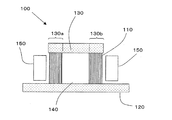
まず、図1を参照しながら、本発明による縦型電界効果トランジスタの基本的な構成を説明する。 First, a basic configuration of a vertical field effect transistor according to the present invention will be described with reference to FIG.
図1に示す縦型電界効果トランジスタ100は、荷電粒子(電子または正孔)を走行させる複数の線状構造物の束から構成された活性領域110を有している。活性領域110を構成する複数の線状構造物の間には隙間が存在する。この隙間は、樹脂などの誘電体材料によって充填されていても良い。活性領域111に含まれる線状構造物の束が全体として、チャネル領域として機能する。線状構造物は、好ましくは、直径がナノメートルオーダのサイズを有するナノワイヤやCNTである。
A vertical
活性領域110は、ソース領域およびドレイン領域として機能する一対の電極(下部電極120および上部電極130)を縦方向に接続している。ソース領域またはドレイン領域として機能する上部電極130は、誘電体部140を介して下部電極120の上に位置しており、誘電体部140の上面から横方向に突出したオーバーハング部分130a、130bを有している。活性領域110の側面部分には、不図示のゲート絶縁膜を介してゲート電極150が対向している。ゲート電極150は、不図示のゲート配線を介して駆動回路に接続されている。駆動回路を用いてゲート電極150の電位を上下させることにより、活性領域110の導電性を制御し、トランジスタ動作(スイッチングや増幅)を実行することができる。
The
本発明による縦型電界効果トランジスタの主たる特徴点は、線状構造物の束から構成された活性領域110が、誘電体部140に支持された上部電極130のオーバーハング部分130a、130bの真下に配置されていることにある。各線状構造物は、好ましくは下部電極120上に成長した柱状半導体から構成されており、活性領域110の外周側面の位置は、上部電極130の側面の位置に整合している。
The main feature of the vertical field effect transistor according to the present invention is that the
本発明による縦型電界効果トランジスタの製造方法によれば、活性領域110の外周側面の位置が、上部電極130の側面の位置に対して自己整合的に規定される。
According to the vertical field effect transistor manufacturing method of the present invention, the position of the outer peripheral side surface of the
次に、図2(a)から(d)を参照しながら、ナノワイヤの束から構成された活性領域110の自己整合的な形成方法の一例を説明する。
Next, an example of a self-aligned formation method of the
まず、図2(a)に示すように、上部電極130が誘電体部140によって下部電極120上に支持された構造を形成する。図2(a)に示される状態において、上部電極130は、誘電体部140の上面よりも横方向に突出したオーバーハング部分130a、130bを有している。誘電体部140は、好適には、パターニングされた絶縁膜から構成される。誘電体部140は、円柱形状、矩形形状、その他の任意の孤立したパターンを有し得るが、基板表面に沿って長く延びた配線形状を有していてもよい。ここで、「孤立したパターン」とは、トランジスタ毎に分離された形状を意味するものとする。
First, as shown in FIG. 2A, a structure in which the
図2(a)に示す構造の形成は、種々の方法によって可能であるが、好ましい形成方法の詳細は後に説明する。 Although the structure shown in FIG. 2A can be formed by various methods, details of a preferable forming method will be described later.
次に、図2(b)に示すように、ナノワイヤ110'を下部電極120上に成長させる。ナノワイヤ110'の成長方法や成長条件の具体例は後に詳述する。ナノワイヤ110'の成長は、図2(c)に示すように、ナノワイヤ110'の上端部が上部電極130の下面に達するまで行なう。図2(b)および(c)に示す例では、ナノワイヤ110'が下部電極120上に選択的に成長している。
Next, as shown in FIG. 2B,
次に、図2(d)に示すように、ナノワイヤ110'のうち、上部電極120で覆われていない部分をエッチングによって除去し、ナノワイヤ110'の束から構成された活性領域110を形成する。このエッチングは、上部電極130をマスクとして行なう。このため、上部電極120は、ナノワイヤ110'に対するエッチャントによってエッチングされにくい材料から形成されていることが好ましい。例えば、上部電極120に白金を用いた時のエッチャントとしては、HBRや塩素ガスが好ましい。また、ナノワイヤ110'の下に位置する下部電極120をエッチングしないようにするためには、下部電極130も、上記のエッチャントに対してエッチングされにくい材料から形成されていることが好ましい。ナノワイヤ110'の不要部分は、異方性エッチングによって除去されることが好ましいが、等方的なエッチングが生じても、それによるエッチング量が少なければ問題は無い。完全な異方性エッチングを行なわなかった場合、活性領域110の外周側面の位置は、上部電極130のオーバーハング部130a、130bのエッジの位置よりも内側にシフトする。本明細書における「整合」は、このようなシフトが発生している状態をも含むものとする。
Next, as shown in FIG. 2D, a portion of the
図2(a)から(d)に示す方法によれば、上部電極130および誘電体部140の形状および配置関係により、活性領域110の形状を規定することができる。図3から図5を参照しながら、このことを説明する。
According to the method shown in FIGS. 2A to 2D, the shape of the
図3(a)は、上部電極130および誘電体部140の配置関係を模式的に示す平面図である。この平面図は、図1に示す下部電極120の側から上部電極130および誘電体部140を見た図面であり、簡単のため、下部電極120の記載は省略している。上部電極130の下面のうち、誘電体部140の上面と接触している部分は図3(a)には現れておらず、上部電極130のうち、誘電体部140の背後に隠れていない部分(はみ出し部分)が、上部電極130のオーバーハング部分である。
FIG. 3A is a plan view schematically showing the positional relationship between the
上部電極130および誘電体部140が図3(a)に示す配置関係を有している場合、活性領域110は、最終的に、図3(b)に示す平面形状を有することになる。すなわち、活性領域110は、上部電極130の真下のうち、誘電体部140が存在していない領域にのみ存在することになる。活性領域110が上部電極130の外側に位置していない理由は、図2(d)を参照して説明したように、上部電極130をマスクとするエッチングによって活性領域110を構成するナノワイヤをエッチングするからである。
When the
本発明で用いる上部電極130および誘電体部140は、図3に示すものに限定されない。図4や図5に示す配置関係であってもよい。
The
図4(a)に示す配置関係によれば、図4(b)に示す活性領域110が形成される。また、図5(a)に示す配置関係によれば、図5(b)に示す活性領域110が形成される。このように、上部電極130および誘電体部140の形状と配置関係を調節することにより、所望の平面形状を有する活性領域110を形成することができる。
According to the arrangement relationship shown in FIG. 4A, the
以下、本発明の好ましい実施形態を説明する。 Hereinafter, preferred embodiments of the present invention will be described.
(実施形態1)
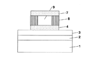
図6(a)および(b)を参照しながら、本発明による縦型電界効果トランジスタの第1の実施形態を説明する。図6(a)は、実施形態の縦型電界効果トランジスタの構成を模式的に示す上面図(上部電極7の記載を省略している)であり、図6(b)は、そのB−B'線断面図である。
(Embodiment 1)
A first embodiment of a vertical field effect transistor according to the present invention will be described with reference to FIGS. FIG. 6A is a top view (illustration of the
本実施形態のトランジスタは、ガラス基板1上に形成された縦型薄膜電界効果型トランジスタ(以下縦型TFTと略す)であり、活性領域8のナノワイヤをキャリアがガラス基板1の主面に垂直な方向に走行する。
The transistor of this embodiment is a vertical thin film field effect transistor (hereinafter abbreviated as vertical TFT) formed on the
本実施形態における活性領域8は、p型不純物がドープされたGeナノワイヤの束から構成されており、この活性領域8は、ドレイン電極として機能する下部電極4と、ソース領域として機能する上部電極7とを縦方向に接続している。
The
下部電極4は、ガラス基板1上に積層された酸化シリコン膜2および透明導電膜3の上に設けられている。透明導電膜3は典型的にはITOから形成されている。なお、酸化シリコン膜2や透明導電膜3は本発明のトランジスタにとって不可欠の構成要素ではない。
The
上部電極7は、誘電体部9を介して下部電極4の上に位置しており、誘電体部9の上面から横方向に突出したオーバーハング部分7a、7bを有している。活性領域8の外周側面には、ゲート絶縁膜6を介してゲート電極5が対向している。
The
このTFTのゲート電極5および上部電極7は、それぞれ、図7に示すように、ゲート配線10およびデータ配線11に接続され、例えば、表示装置などのスイッチング素子として機能させることができる。本実施形態のTFTを、液晶表示装置におけるアクティブマトリクス基板上のTFTとして用いる場合は、図7に示すゲート配線10が走査線(ケートバス)として機能し、ゲートバス・ドライバからの信号によってTFTのオン・オフを制御する。一方、データ配線11は、ソースバスとして機能し、ソースバス・ドライバからの信号によって透明導電膜3の電位を変化させる。透明導電膜3は、個々の画素を規定し、不図示の対向電極との間でキャパシタを形成する。このキャパシタに蓄えられる電荷の量によって透明導電膜3と対向電極との間に画素毎に異なる電界が形成され、液晶の配向状態が制御させることになる。液晶の配向状態を画素単位で調節することにより、液晶層を透過する光の偏光状態が変化するため、画素配列によって構成される2次元的な像を形成することが可能になる。
As shown in FIG. 7, the
上記の説明では、透過型の液晶表示装置に本実施形態のTFTを用いているが、このTFTは、反射型液晶表示装置や有機ELのTFTとしても用いることができ、また、撮像装置や集積回路におけるTFTとしても用いることが可能である。なお、撮像装置や集積回路を形成する場合、図6(b)に示す透明導電膜3は不要である。
In the above description, the TFT of this embodiment is used for a transmissive liquid crystal display device. However, this TFT can also be used as a reflective liquid crystal display device or an organic EL TFT, and can also be used as an imaging device or an integrated device. It can also be used as a TFT in a circuit. When forming an imaging device or an integrated circuit, the transparent
本実施形態では、TFTを支持する基板としてガラス基板1を用いているが、基板は、ガラス基板に限定されず、例えば、酸化シリコン、窒化シリコン、酸化アルミニウム、酸化チタン、アクリル樹脂、エポキシ樹脂、ポリイミド等などの絶縁物から形成された任意の基板を用いることが可能である。なお、基板の全体が絶縁物から形成されている必要はないため、基板は、シリコン基板、SOI基板、化合物半導体基板であってもよい。
In this embodiment, the
再び、図6(b)を参照する。 Reference is again made to FIG.
上部電極7のうち、誘電体部9の上面から横方向に延びるオーバーハング部7a、7bの各々の横方向サイズは、10nm以上であることが好ましく、50〜100nm程度の範囲内にあることが更に好ましい。誘電体部9の高さは、活性領域8の高さ(基板主面に垂直方向のサイズ)を規定しており、必要なチャネル長に応じて任意の大きさに設計され得る。本実施形態では、誘電体部9の高さを例えば50nm以上1μm以下の大きさに設定する。
Of the
活性領域8を構成するナノワイヤは、種々の半導体材料から形成され得るが、本実施形態では、Geから形成されたナノワイヤを用いて活性領域8を形成している。Geのナノワイヤは、VLS(Vapor−Liquid−Solid)成長メカニズムにより、CVD法によって触媒金属から好適に成長させられる。この方法によれば、直径が1nm〜100nmの範囲内に制御されたナノワイヤを成長させることができる。
The nanowires constituting the
Geナノワイヤの成長に適した触媒金属は、たとえば、金、鉄、コバルト、ニッケルのような遷移金属、または、それら遷移金属の合金である。触媒金属は、任意の方法で形成され得るが、たとえば、基板上に堆積した触媒金属薄膜に対して熱処理を施すことにより形成された触媒微粒子を用いても良い。本実施形態では、1つの活性領域を構成するナノワイヤの束は、10本から10万本程度のナノワイヤから構成される。 Suitable catalytic metals for the growth of Ge nanowires are, for example, transition metals such as gold, iron, cobalt, nickel, or alloys of these transition metals. The catalyst metal can be formed by any method. For example, catalyst fine particles formed by performing a heat treatment on the catalyst metal thin film deposited on the substrate may be used. In the present embodiment, the bundle of nanowires constituting one active region is composed of about 100,000 to 100,000 nanowires.
下部電極4および上部電極7は、種々の導電材料から形成され得る。下部電極4の上にGeナノワイヤを成長させるという観点からは、下部電極4を例えば金、銀、白金のような金属やコバルトやニッケルとのシリサイドから形成することが好ましい。触媒として機能しない導電性材料から下部電極4を形成する場合は、下部電極4の表面に触媒金属の微粒子を配置することが望ましい。
The
活性領域8とゲート電極5とを絶縁するゲート絶縁膜6の材料は、たとえば、酸化シリコン、窒化シリコン、酸化アルミニウム、酸化ゲルマニウム、酸化ハフニウムなどの絶縁材料から形成される。ゲート電極5は、例えば金、銀、白金、モリブデン、クロム、多結晶シリコンなどの導電性材料から形成される。
The material of the
本実施形態では、上部電極7のオーバーハング部分7a、7bの真下に自己整合的に配置したGeナノワイヤを用いて縦型の活性領域8を形成しているため、上部電極7を支持する誘電体部9の高さを調節することにより、TFTのチャネル長を制御することができる。誘電体部9は、堆積した絶縁膜をパターニングすることによって好適に作製され得る。この方法によって誘電体部9を形成する場合、誘電体部9の高さは堆積する絶縁膜の厚さによって規定される。堆積する絶縁膜の厚さは、高精度で制御できるため、本実施形態におけるTFTのチャネル長も高精度で制御され得る。このため、リソグラフィ技術の微細化可能限界に制約されることなく、トランジスタのチャネル長を短縮し、集積度の向上をはかることが可能になる。さらに、縦型TFT構造によれば、従来の横型TFTに比べ、TFTの占有面積を縮小できるため、透過型液晶表に装置のスイッチング素子に用いた場合、開口率を向上させることができる。
In the present embodiment, since the vertical
[製造方法]
以下、図8〜図10を参照しながら、本実施形態のTFTを製造する方法の好ましい実施形態を説明する。
[Production method]
Hereinafter, a preferred embodiment of a method for manufacturing the TFT of this embodiment will be described with reference to FIGS.
まず、図8(a)に示すように、ガラス基板1上に酸化シリコン膜2、ITO膜3、下部電極(ドレイン電極)4となる第1導電体膜4'、誘電体部9となる絶縁膜9'、および上部電極(ソース電極)7となる第2導電体膜7'をこの順番で積層する。下部電極4および上部電極7は、金、銀、多結晶シリコンのような導電性材料をスパッタリング法やCVD法によって堆積することによって形成される。また、誘電体部8は、例えば酸化シリコンや窒化シリコンなどの絶縁材料をスパッタリング法やCVD法によって堆積することによって形成される。
First, as shown in FIG. 8A, on a
次に、フォトリソグラフィ技術により、第2導電体膜7'の上にレジストマスク(不図示)を形成した後、異方性エッチング技術により、第2導電体膜7'をパターニングして、図8(b)に示す上部電極(ソース電極)7および誘電体部9を形成する。
Next, after forming a resist mask (not shown) on the
レジストマスクを酸素系プラズマエッチングによって除去した後、ウェットエッチングにより、誘電体部9に対するサイドエッチを行ない、図9(a)に示す構造を得る。誘電体部9のサイドエッチは、下部電極4となる第1導電体膜4'および上部電極7をほとんどエッチングしないエッチング条件のもとで誘電体部9を優先的にエッチングすることが好ましい。誘電体部9のサイドエッチは等方的に進行するため、誘電体部9の側面を部分的にマスクしない限り、誘電体部9の側面は均一にエッチングされ、例えば図3に示すような構造が形成される。したがって、図4および図5に示すような構造を形成するためには、誘電体部9の側面の一部をマスクし、マスクされていない部分からサイドエッチを進行させる必要がある。
After removing the resist mask by oxygen-based plasma etching, side etching is performed on the
このようなサイドエッチは、ウェットエッチングによって行なうことが好ましい。誘電体部9が酸化シリコンから形成されている場合、エッチャントとしてはフッ酸溶液を用いることができる。誘電体部9が窒化シリコンから形成されている場合は、熱リン酸を用いることができる。エッチングレート及びエッチング時間を制御することにより、サイドエッチの深さ(横方向のエッチング深さ)を調節することができる。本実施形態では、このサイドエッチの深さを調節することにより、オーバーハング部分7a、7bのサイズを、10nm以上、例えば50〜100nm程度に設定する。
Such side etching is preferably performed by wet etching. When the
次に、図9(b)に示すように、CVD法によって下部電極4の表面上にナノワイヤ8'を成長させる。Geナノワイヤを成長させる場合は、ゲルマンガスを使用するが、Siナノワイヤを成長させる場合、シランやジシランガスを使用する。
Next, as shown in FIG. 9B,
下部電極4を触媒金属から形成しない場合は、CVD法によるナノワイヤの成長を開始する前、触媒として、例えばNi、Coなどの遷移金属微粒子、または、そのような遷移金属の合金の微粒子を下地表面上に堆積しておくことが好ましい。このような触媒の堆積法としては、例えば、ナノワイヤ成長前に、溶媒中にある金属微粒子を分散させる方法や、触媒となる金属薄膜に熱処理を行うことで凝集させ、微粒子化する方法を用いることができる。
In the case where the
次に、図10(a)に示すように、異方性のエッチングを行なうことにより、ナノワイヤ8'のうち、上部電極7によって覆われていない部分を選択的に除去する。上部電極7をエッチングマスクとして用いるため、残ったナノワイヤ8'によって構成される活性領域8の外側面は、上部電極7のエッジに自己整合する。活性領域8の横方向サイズは、上部電極7のオーバーハング部分7a、7bの横方向サイズによって規定されるため、フォトリソグラフィ技術による微細化の限界に制約されることなく、活性領域8を小さくすることが可能である。
Next, as shown in FIG. 10A, anisotropic etching is performed to selectively remove portions of the
なお、ナノワイヤ8'のうち、活性領域8として機能させるべき部分以外の部分を選択的に除去するには、まず、基板全面に塩素系ガスを用いた異方性エッチ処理を行った後、洗浄等を行えばよい。
In order to selectively remove a portion of the
次に、ゲート絶縁膜6を堆積した後、図10(b)に示すように、ゲート電極形成領域を規定する開口部を有するレジストパターン15を形成する。ゲート絶縁膜6は、例えば酸化シリコン、窒化シリコン、または酸化ハフニウムのような絶縁体から形成され得る。ゲート電極5を形成するための電極材料をレジストバターン15上に堆積すると、レジストパターン15の開口部内では、ゲート電極5が形成されるべき位置に電極材料が堆積する。この後、レジストパターン15を除去することにより、ゲート電極材料からなる膜の不要部分をリフトオフして、図11(a)に示すゲート電極5を形成することができる。次に、第1導電体膜4'および上部電極7の上に存在するゲート絶縁膜6の不要部分をウェットエッチングによって除去する。
Next, after depositing the
なお、本実施形態では、リフトオフによってゲート電極5を形成しているが、ゲート絶縁膜6上にゲート電極材料からなる膜を堆積した後、この膜に対してエッチバックや研磨処理を行うことにより、ゲート電極5を形成してもよい。
In this embodiment, the
次に、図11(b)に示すように、第1導電体膜4'をパターニングすることにより、ドレイン電極として機能する下部電極4を形成する。その後、リソグラフィおよびエッチング技術により、透明導電膜3をパターニングして、例えば図7に示すように画素電極の形状に加工する。本実施形態では、上部電極7およびゲート電極5をマスクとして第1導電体膜4'をパターニンングしているため、下部電極4のためのフォトマスクが不要である。ただし、下部電極4の形状を規定するフォトマスクを用意し、任意の形状を有するように下部電極4をパターニングしてもよい。
Next, as shown in FIG. 11B, the
以上説明してきたように、本実施形態による縦型TFTの製造法によれば、ナノワイヤ8'を成長させた後、リソグラフィ工程を行なうことなく、ナノワイヤ8'のうち不要な部分を上部電極7に対して「自己整合的」に除去することができる。このため、ナノワイヤ8'からなる活性領域8の位置および形状を高い精度で制御できる。また、マスクアライメント用のマージンを設ける必要がなくなるため、更なる微細化が可能になる。
As described above, according to the method of manufacturing the vertical TFT according to the present embodiment, after the
なお、ナノワイヤ8'を成長させた後、その上に上部電極7となる第2導電体膜7'を堆積しようとすると、多数のナノワイヤ8'の隙間に第2導電体膜を構成する導電材料が進入するため、半導体特性を示す活性領域8を形成できない。これに対し、本実施形態では、ナノワイヤ8'の成長に先立って上部電極7を形成しているため、このような問題を回避できる。
When the
このように本実施形態によれば、チャネル長がフォトリソグラフィの精度に依存しないため、微細なチャネルを高い制度で実現できる。その結果、チャネル長のバラツキに起因するトラジスタ特性の変動を抑制することもできる。 As described above, according to this embodiment, since the channel length does not depend on the accuracy of photolithography, a fine channel can be realized with a high system. As a result, it is possible to suppress fluctuations in transistor characteristics due to variations in channel length.
図12は、本実施形態のTFTが複数配列された半導体集積回路装置の一部を模式的に示す断面図である。図12では、2種類のトランジスタが図示されているが、好ましい例では、多数のトランジスタが同一基板上に集積される。図12に示す装置では、透明導電膜3が設けられておらず、各トランジスタは、不図示の配線によって相互接続される。このような半導体集積回路装置は、例えば表示装置の駆動回路などに好適に用いられる。
FIG. 12 is a cross-sectional view schematically showing a part of a semiconductor integrated circuit device in which a plurality of TFTs of this embodiment are arranged. Although two types of transistors are shown in FIG. 12, in a preferred example, a large number of transistors are integrated on the same substrate. In the apparatus shown in FIG. 12, the transparent
図12に示す2つのトランジスタは、それぞれ、n型不純物がドープされた半導体ナノワイヤからなるn型活性領域13およびp型不純物がドープされた半導体ナノワイヤからなるp型活性領域14を有しており、不図示の配線を介してCMOS回路を形成するように相互接続されている。
Each of the two transistors shown in FIG. 12 has an n-type
(実施形態2)
以下、図13から図15を参照しながら、本発明による縦型電界効果トランジスタの第2の実施形態を説明する。
(Embodiment 2)
Hereinafter, a vertical field effect transistor according to a second embodiment of the present invention will be described with reference to FIGS.
図13に示す縦型電界効果トランジスタは、基本的には、実施形態1における縦型電界効果トランジスタの構成と同様の構成を有しており、異なる点は、下部電極4の形状およびそのパターニング方法の差異にある。
The vertical field effect transistor shown in FIG. 13 basically has the same configuration as that of the vertical field effect transistor in the first embodiment, except that the shape of the
以下、図面を参照しながら、本実施形態の製造方法を説明する。 Hereinafter, the manufacturing method of the present embodiment will be described with reference to the drawings.
まず、図14(a)に示すように、酸化シリコン膜2、透明導電膜3、下部電極4となる第1導電体膜4'、絶縁膜9'、および上部電極7となる第2導電体膜7'を、この順序で絶縁基板1上に堆積する。
First, as shown in FIG. 14A, the
次に、図14(b)に示すように、リソグラフィおよび異方性エッチング技術により、第2導電体膜7'、絶縁膜9'、および第1導電体膜4'をパターニングし、それによって上部電極7、誘電体部9、および下部電極4を形成する。このパターニングに際しては、上部電極7の形状および位置を規定するレジストパターン(不図示)を第2導電体膜7'上に形成するが、このレジストパターンは、パターニングが終了した後、酸素系プラズマエッチングによって除去される。
Next, as shown in FIG. 14B, the
次に、図15(a)に示すように、ウェットエッチングにより、誘電体部9に対するサイドエッチを行ない、上部電極7のオーバーハング部7a、7bを形成する。ウェットエッチングのための薬液や、絶縁膜9'の材料を適切に選択することにより、上記のパターンに際して透明導電膜3を殆んどエッチングしないようにすることができる。具体的には、透明導電膜3のエッチングレートは、下部電極4'のエッチングの1/10以下に抑えることが好ましい。
Next, as shown in FIG. 15A, side etching is performed on the
次に、図15(b)に示すように、実施形態1で行なったナノワイヤ8'の成長と同様の方法によってナノワイヤ8'を成長させる。ただし、本実施形態では、上部電極7と同様の形状を有するようにパターニングされた下部電極4の表面に対して、ナノワイヤを選択的に成長させている。このため、透明導電膜3上にはナノワイヤ8'がほとんど成長しない。図15(b)に示すように、下部電極4の側面から横方向に成長するナノワイヤ8'も存在するが、下部電極4の側面のサイズ(下部電極4の厚さ)は50〜200nm程度であるため、下部電極4の側面上に成長するナノワイヤ8'の量は相対的に少ない。また、この不要なナノワイヤは、上部電極7によって覆われていない領域に存在するため、上部電極7をマスクとする異方性エッチングを行なうことにより、容易に除去することができる。こうして不要なナノワイヤをエッチングすることにより、図13に示す構造を形成ができる。この後、実施形態1における製造方法と同様の製造方法を実施すれば、最終的な縦型薄膜トランジスタを得ることができる。
Next, as shown in FIG. 15B, the
ナノワイヤ8'の成長に必要な触媒は、下部電極4となる第1導電体膜4'を堆積した後、第1導電体膜4'の上面に配置してもよい。このようにすると、図15(a)に示すようにパターニングされた下部電極4の上面に存在するが、その側面には、ほとんど存在しななくなる。このため、ナノワイヤ8'は下部電極4の上面に選択的に成長し、下部電極4の側面には殆んど成長しなくなり、図15(b)を参照しながら説明した特別のエッチングが不要になる。
The catalyst necessary for the growth of the
本実施形態の製造方法によれば、下部電極4のパターニングを、上部電極7に対して自己整合的に行なうことができるため、下部電極4のためのフォトマスクを別途用意する必要が無くなり、また、そのようなフォトマスクのためのマスクアライメント工程も不要になる。
According to the manufacturing method of this embodiment, since the patterning of the
(実施形態3)
次に、図16を参照しながら、本発明による縦型電界効果トランジスタの第3の実施形態を説明する。
(Embodiment 3)
Next, a third embodiment of the vertical field effect transistor according to the present invention will be described with reference to FIG.
図16に示す縦型電界効果トランジスタ160が図1の縦型電界効果トランジスタ100と異なる点は、円柱状のゲート電極150が誘電体部140の中央部に位置している点にある。この点を除いて、トランジスタ160とトランジスタ100は同一の構成を有している。
The vertical
上部電極130が誘電体部140を介して下部電極120の上に位置しており、誘電体部140の上面から横方向に突出したオーバーハング部130aを有している点は、図1の上部電極130と同様である。しかし、図16に示す上部電極130の中央部には、ゲート電極150を不図示の配線に接続するための開口部が設けられている。この開口部は、活性領域110を構成するナノワイヤ110'の成長を行う前において、上部電極130のパターニングを行なうときに形成することが好ましい。
The
なお、1つの縦型電界効果トランジスタ160が、図16に示すゲート電極150に加えて、図1に示すゲート電極150を備えていても良い。
Note that one vertical
以下に、図17(a)から(c)を参照しながら、本実施形態の製造方法の一例を説明する。 Below, an example of the manufacturing method of this embodiment is demonstrated, referring FIG. 17 (a) to (c).
まず、前述の実施形態について説明した方法と同様の方法により、図17(a)に示すように上部電極130が誘電体部140によって下部電極120上に支持された構造を形成する。
First, a structure in which the
次に、図17(b)に示すように、上部電極130の中央部をエッチングすることにより、上部電極130の中央に円柱状の第1開口部を形成する。この開口部は、例えば公知のリソグラフィ技術および異方性エッチング技術によって形成できる。エッチングの前には、開口部の位置および形状を規定するレジストパターン(不図示)を上部電極130上に形成するが、このレジストパターンは、エッチングが終了した後、酸素系プラズマエッチングによって除去される。
Next, as shown in FIG. 17B, a cylindrical first opening is formed in the center of the
次に、図17(c)に示すように、誘電体部140の中央部にゲート電極を形成する。具体的には、リソグラフィ技術およびエッチング技術により、誘電体部140の中央部を異方的にエッチングし、誘電体部140の中央に円柱状の第2開口部を形成する。第2開口部の直径は、上部電極130の中央部に形成した第1開口部の直径よりも、例えば200nmから400nm程度は小さく設定することが好ましい。
Next, as shown in FIG. 17C, a gate electrode is formed at the center of the
その後、例えばリフトオフ法などにより、上記第1および第2開口部に円柱状のゲート電極150を形成することができる。
Thereafter, the
図17(c)に示す工程の後は、前述した実施形態で用いた方法と同様の方法により、ナノワイヤ110'を所望の領域に成長させることにより、図16のトランジスタ160を形成することができる。
After the step shown in FIG. 17C, the
(実施形態4)
次に、図18を参照しながら、本発明による縦型電界効果トランジスタの第4の実施形態を説明する。
(Embodiment 4)
Next, a fourth embodiment of the vertical field effect transistor according to the present invention will be described with reference to FIG.
図18に示すトランジスタ170が図16のトランジスタ160と異なる点は、トランジスタ160では、誘電体部140がゲート絶縁膜として機能するのに対して、本実施形態のトランジスタ170では、誘電体部140とは別にゲート絶縁膜180を備えている点にある。この点を除けば、トランジスタ170およびトランジスタ160は、実質的に同一の構成を有している。
The
図18(a)に示されるように、本実施形態における上部電極130も、誘電体部140を介して下部電極120の上に位置しており、誘電体部140の上面から横方向に突出したオーバーハング部130aを有している。また、図18(b)に示されるように、上部電極130は、活性領域110の外側に広がる誘電体部140の上面を覆っている。
As shown in FIG. 18A, the
以下に、図19(a)から(c)を参照しながら、本実施形態の製造方法の一例を説明する。 Below, an example of the manufacturing method of this embodiment is demonstrated, referring FIG. 19 (a) to (c).
まず、前述の実施形態について説明した方法と同様の方法により、図19(a)に示すように上部電極130が誘電体部140によって下部電極120上に支持された構造を形成する。ただし、複数の円柱状開口部が設けられた一枚の絶縁層パターンを有するように加工されている。
First, a structure in which the
次に、図19(b)に示すように、円柱状の開口部の内部を埋めるようにゲート絶縁膜180およびゲート電極150の材料となる膜を、この順序で堆積する。これらの膜は、蒸着法、スパッタ法、またはCVD法などの各種の薄膜堆積方法で堆積され得る。
Next, as shown in FIG. 19B, films serving as materials for the
次に、図19(c)に示すように、ゲート電極150およびゲート絶縁膜180のうち、上部電極130の上に存在する部分をエッチバック法または研磨法によって除去・平坦化し、ゲート電極150およびゲート絶縁膜180を最終的な形状に加工する。
Next, as shown in FIG. 19C, portions of the
上記いずれの実施形態においても、VLS法によってナノワイヤを成長させるため、その成長温度を低温ポリシリコンの成長温度に比べて低下できる。このため、耐熱性の高い高価な基板を用いることなく、薄膜トランジスタを製造することが可能になる。また、ナノワイヤの成長温度を更に低下させることができれば、プラスチック基板のような低融点基板上にナノワイヤを形成することも可能となり、フレキシブルディスプレイや有機ELの駆動回路を実現できる可能性がある。 In any of the above embodiments, since the nanowire is grown by the VLS method, the growth temperature can be lowered as compared with the growth temperature of the low-temperature polysilicon. Therefore, a thin film transistor can be manufactured without using an expensive substrate with high heat resistance. Further, if the growth temperature of the nanowire can be further lowered, it is possible to form the nanowire on a low melting point substrate such as a plastic substrate, and there is a possibility that a flexible display or an organic EL drive circuit can be realized.
なお、VLS法によって成長させたナノワイヤは、単結晶構造を有しているため、高移動度の実現が期待でき、高速動作が求められる駆動回路の形成も可能となり、高性能なシステムオンディスプレイを実現することもできる。 Since nanowires grown by the VLS method have a single crystal structure, high mobility can be expected, and drive circuits that require high-speed operation can be formed. It can also be realized.
以上説明してきたように、本発明によれば、ナノワイヤからなる活性領域を必要な領域に自己整合的に形成することができる。また、チャネル長の制御がリソグラフィの精度に依存しないため、フォトリソグラフィでは実現が困難な微細チャネル長を実現することができる。また、トランジスタとして縦型構造を採用しているため、個々のトランジスタ素子のサイズを縮小し、集積度を向上させやすい。 As described above, according to the present invention, an active region made of nanowires can be formed in a necessary region in a self-aligned manner. In addition, since the control of the channel length does not depend on the accuracy of lithography, it is possible to realize a fine channel length that is difficult to realize by photolithography. Further, since a vertical structure is adopted as the transistor, the size of each transistor element can be reduced and the degree of integration can be easily improved.
以上の各実施形態では、線状構造物としてナノワイヤを用いたトランジスタを説明してきたが、ナノワイヤに代えてCNTを用いても良い。 In the above embodiments, transistors using nanowires as linear structures have been described, but CNTs may be used instead of nanowires.
本発明による縦型電界効果トランジスタは、高移動度チャネルを実現でき、システムLSI等のロジックICとして有用である。さらにナノワイヤの成長は低温成長可能なため、ガラスやプラスチック基板上に成長し、システムオンディスプレイやシートディスプレイ等として有用である。 The vertical field effect transistor according to the present invention can realize a high mobility channel and is useful as a logic IC such as a system LSI. Furthermore, since nanowires can be grown at low temperatures, they grow on glass or plastic substrates and are useful as system-on-displays, sheet displays, and the like.
1 基板
2 酸化シリコン膜
3 透明導電膜
4 下部電極
4' 第1導電体膜
5 ゲート電極
6 ゲート絶縁膜
7 上部電極
7' 第2導電体膜
7a 上部電極7のオーバーハング部分
7b 上部電極7のオーバーハング部分
8 活性領域
8' ナノワイヤ
9 誘電体部
9' 絶縁膜
13 n型チャネル領域
14 p型チャネル領域
15 レジストパターン
100 縦型電界効果トランジスタ
110 活性領域
120 下部電極
130 上部電極
140 誘電体部
130a オーバーハング部分
130b オーバーハング部分
150 ゲート電極
160 縦型電界効果トランジスタ
DESCRIPTION OF
Claims (23)
前記活性領域の下端に接続され、ソース領域およびドレイン領域の一方として機能する下部電極と、
前記活性領域の上端に接続され、前記ソース領域およびドレイン領域の他方として機能する上部電極と、
前記活性領域に含まれる線状構造物の束の少なくとも一部における導電性を制御するゲート電極と、
前記活性領域と前記ゲート電極との間に配置され、前記ゲート電極を前記線状構造物の束から電気的に絶縁するゲート絶縁膜と、
を備えた縦型電界効果トランジスタであって、
前記上部電極と前記下部電極との間に配置され、前記上部電極の側面に対して内側に外周側面を有した誘電体部を更に備え、
前記上部電極は、前記誘電体部を介して、前記下部電極の上に位置し、しかも、前記誘
電体部の上面から横方向に突出し、前記誘電体部とは離間したオーバーハング部分を有しており、
前記活性領域は前記誘電体部の外周側面の外側で前記上部電極のオーバーハング部分の真下に配置されている、縦型電界効果トランジスタ。An active region having a bundle of a plurality of linear structures that function as channel regions for running charged particles;
A lower electrode connected to the lower end of the active region and functioning as one of a source region and a drain region;
An upper electrode connected to an upper end of the active region and functioning as the other of the source region and the drain region;
A gate electrode for controlling conductivity in at least a part of a bundle of linear structures included in the active region;
A gate insulating film disposed between the active region and the gate electrode to electrically insulate the gate electrode from the bundle of linear structures;
A vertical field effect transistor comprising:
Further comprising a dielectric part disposed between the upper electrode and the lower electrode and having an outer peripheral side surface on the inner side with respect to the side surface of the upper electrode ;
The upper electrode is located on the lower electrode through the dielectric portion, and has an overhang portion protruding laterally from the upper surface of the dielectric portion and spaced apart from the dielectric portion. And
The vertical field effect transistor, wherein the active region is disposed outside an outer peripheral side surface of the dielectric portion and immediately below an overhang portion of the upper electrode.
前記上部電極の下面は、前記誘電体部または前記活性領域と接触している、請求項1から4の何れかに記載の縦型電界効果トランジスタ。The dielectric part is formed of an electrically insulating material that supports the upper electrode,
The vertical field effect transistor according to any one of claims 1 to 4, wherein a lower surface of the upper electrode is in contact with the dielectric portion or the active region.
前記複数の電界効果トランジスタの少なくとも1つは、
荷電粒子を走行させるチャネル領域として機能する複数の線状構造物の束を有する活性領域と、
前記活性領域の下端に接続され、ソース領域およびドレイン領域の一方として機能する下部電極と、
前記活性領域の上端に接続され、前記ソース領域およびドレイン領域の他方として機能する上部電極と、
前記活性領域に含まれる線状構造物の束の少なくとも一部における導電性を制御するゲート電極と、
前記活性領域と前記ゲート電極との間に配置され、前記ゲート電極を前記線状構造物の束から電気的に絶縁するゲート絶縁膜と、
を備えた縦型電界効果トランジスタであって、
前記上部電極と前記下部電極との間に配置され、前記上部電極の側面に対して内側に外周側面を有した誘電体部を更に備え、
前記上部電極は、前記誘電体部を介して、前記下部電極の上に位置し、しかも、前記誘電体部の上面から横方向に突出し、前記誘電体部とは離間したオーバーハング部分を有しており、
前記活性領域は前記誘電体部の外周側面の外側で前記上部電極のオーバーハング部分の真下に配置されている、電子装置。An electronic device comprising a substrate and a plurality of field effect transistors formed on the substrate,
At least one of the plurality of field effect transistors is:
An active region having a bundle of a plurality of linear structures that function as channel regions for running charged particles;
A lower electrode connected to the lower end of the active region and functioning as one of a source region and a drain region;
An upper electrode connected to an upper end of the active region and functioning as the other of the source region and the drain region;
A gate electrode for controlling conductivity in at least a part of a bundle of linear structures included in the active region;
A gate insulating film disposed between the active region and the gate electrode to electrically insulate the gate electrode from the bundle of linear structures;
A vertical field effect transistor comprising:
Further comprising a dielectric part disposed between the upper electrode and the lower electrode and having an outer peripheral side surface on the inner side with respect to the side surface of the upper electrode ;
The upper electrode is located on the lower electrode through the dielectric portion, and has an overhang portion protruding laterally from the upper surface of the dielectric portion and spaced apart from the dielectric portion. And
The electronic device is an electronic device, wherein the active region is disposed outside an outer peripheral side surface of the dielectric portion and immediately below an overhang portion of the upper electrode.
表示装置として動作する請求項9に記載の電子装置。The field effect transistors are arranged in a matrix for each pixel on the substrate,
The electronic device according to claim 9, which operates as a display device.
前記上部電極と前記下部電極との間に誘電体部が挟まれ、前記上部電極が前記誘電体部の上面から横方向に突出したオーバーハング部分を有している構造を形成する工程(A)と、
前記下部電極の上面において前記誘電体部が存在していない領域から前記上部電極におけるオーバーハング部分の下面に達するように複数の線状構造物の束を成長させる工程(B)と、
を含む、製造方法。An active region having a bundle of a plurality of linear structures functions as a channel region for running a load conductive particles, connected to the lower end of the active region, and a lower electrode functioning as one of a source region and a drain region, the active An upper electrode connected to the upper end of the region and functioning as the other of the source region and the drain region; a gate electrode for controlling conductivity in at least a part of a bundle of linear structures included in the active region; A method of manufacturing a vertical field-effect transistor comprising a gate insulating film disposed between a region and the gate electrode, and electrically insulating the gate electrode from the bundle of linear structures,
A step of forming a structure in which a dielectric portion is sandwiched between the upper electrode and the lower electrode, and the upper electrode has an overhang portion protruding laterally from the upper surface of the dielectric portion (A) When,
A step (B) of growing a bundle of a plurality of linear structures so as to reach a lower surface of an overhang portion in the upper electrode from a region where the dielectric portion does not exist on the upper surface of the lower electrode;
Manufacturing method.
前記上部電極と前記下部電極との間に誘電体部が挟まれた構造を形成する工程(a1)と、
前記誘電体部の側面の少なくとも一部をサイドエッチによってセットバックさせる工程(a2)と、
を含む、請求項14に記載の製造方法。The step (A)
Forming a structure in which a dielectric portion is sandwiched between the upper electrode and the lower electrode (a1);
A step (a2) of setting back at least a part of the side surface of the dielectric portion by side etching;
The manufacturing method of Claim 14 containing these.
前記下部電極のための第1導電体膜を形成する工程と、
絶縁膜を前記第1導電体膜上に形成する工程と、
前記上部電極のための第2導電体膜を前記絶縁膜上に形成する工程と、
前記上部電極の位置および形状を規定するマスク層を前記第2導電体膜上に形成する工程と、
前記第2導電体膜のうち前記マスク層で覆われてない部分をエッチングすることにより、前記第2導電体膜から前記上部電極を形成する工程と、
前記絶縁膜をエッチングすることにより、前記誘電体部を形成する工程と、
前記第1導電体膜をパターニングすることにより、前記第1導電体膜から前記下部電極を形成する工程と、
を含む、請求項14に記載の製造方法。The step (a1)
Forming a first conductor film for the lower electrode;
Forming an insulating film on the first conductor film;
Forming a second conductor film for the upper electrode on the insulating film;
Forming a mask layer defining the position and shape of the upper electrode on the second conductor film;
Forming the upper electrode from the second conductor film by etching a portion of the second conductor film that is not covered with the mask layer;
Etching the insulating film to form the dielectric portion;
Forming the lower electrode from the first conductor film by patterning the first conductor film;
The manufacturing method of Claim 14 containing these.
前記下部電極のための第1導電体膜を形成する工程と、
絶縁膜を前記第1導電体膜上に形成する工程と、
前記上部電極のための第2導電体膜を前記絶縁膜上に形成する工程と、
前記上部電極の位置および形状を規定するマスク層を前記第2導電体膜上に形成する工程と、
前記第2導電体膜のうち前記マスク層で覆われていない部分をエッチングすることにより、前記第2導電体膜から前記上部電極を形成する工程と、
前記上部電極をマスクとして前記絶縁膜をエッチングすることにより、前記誘電体部を形成する工程と、
を含む、請求項14に記載の製造方法。The step (a1)
Forming a first conductor film for the lower electrode;
Forming an insulating film on the first conductor film;
Forming a second conductor film for the upper electrode on the insulating film;
Forming a mask layer defining the position and shape of the upper electrode on the second conductor film;
Forming the upper electrode from the second conductor film by etching a portion of the second conductor film that is not covered with the mask layer;
Etching the insulating film using the upper electrode as a mask to form the dielectric portion; and
The manufacturing method of Claim 14 containing these.
Applications Claiming Priority (3)
| Application Number | Priority Date | Filing Date | Title |
|---|---|---|---|
| JP2004291170 | 2004-10-04 | ||
| JP2004291170 | 2004-10-04 | ||
| PCT/JP2005/017830 WO2006038504A1 (en) | 2004-10-04 | 2005-09-28 | Vertical field effect transistor and method for making the same |
Publications (2)
| Publication Number | Publication Date |
|---|---|
| JPWO2006038504A1 JPWO2006038504A1 (en) | 2008-05-15 |
| JP4568286B2 true JP4568286B2 (en) | 2010-10-27 |
Family
ID=34956325
Family Applications (1)
| Application Number | Title | Priority Date | Filing Date |
|---|---|---|---|
| JP2006539239A Expired - Fee Related JP4568286B2 (en) | 2004-10-04 | 2005-09-28 | Vertical field effect transistor and manufacturing method thereof |
Country Status (4)
| Country | Link |
|---|---|
| US (1) | US7586130B2 (en) |
| JP (1) | JP4568286B2 (en) |
| CN (1) | CN100490180C (en) |
| WO (1) | WO2006038504A1 (en) |
Cited By (1)
| Publication number | Priority date | Publication date | Assignee | Title |
|---|---|---|---|---|
| US9679965B1 (en) | 2015-12-07 | 2017-06-13 | Samsung Electronics Co., Ltd. | Semiconductor device having a gate all around structure and a method for fabricating the same |
Families Citing this family (71)
| Publication number | Priority date | Publication date | Assignee | Title |
|---|---|---|---|---|
| KR100574317B1 (en) * | 2004-02-19 | 2006-04-26 | 삼성전자주식회사 | Gate structure, semiconductor device having the same and methods of forming the gate structure and semiconductor device |
| CN101010780B (en) * | 2004-04-30 | 2012-07-25 | 纳米系统公司 | Systems and methods for nanowire growth and harvesting |
| US7230286B2 (en) * | 2005-05-23 | 2007-06-12 | International Business Machines Corporation | Vertical FET with nanowire channels and a silicided bottom contact |
| US20060281321A1 (en) * | 2005-06-13 | 2006-12-14 | Conley John F Jr | Nanowire sensor device structures |
| US7446372B2 (en) * | 2005-09-01 | 2008-11-04 | Micron Technology, Inc. | DRAM tunneling access transistor |
| TWI300251B (en) * | 2006-07-14 | 2008-08-21 | Ind Tech Res Inst | Manufacturing method of vertical thin film transistor |
| KR20090057089A (en) * | 2006-09-04 | 2009-06-03 | 코닌클리즈케 필립스 일렉트로닉스 엔.브이. | Control of carbon nanostructure growth in an interconnect structure |
| US7573420B2 (en) * | 2007-05-14 | 2009-08-11 | Infineon Technologies Ag | RF front-end for a radar system |
| JP4531850B2 (en) * | 2007-03-23 | 2010-08-25 | パイオニア株式会社 | Organic transistor and manufacturing method thereof |
| WO2009023304A2 (en) * | 2007-05-02 | 2009-02-19 | Atomate Corporation | High density nanotube devices |
| EP2019313B1 (en) * | 2007-07-25 | 2015-09-16 | Stichting IMEC Nederland | Sensor device comprising elongated nanostructures, its use and manufacturing method |
| KR100900148B1 (en) * | 2007-10-31 | 2009-06-01 | 주식회사 하이닉스반도체 | Semicoductor device and method of fabricating the same |
| WO2009064842A1 (en) * | 2007-11-13 | 2009-05-22 | William Marsh Rice Unvirsity | Vertically-stacked electronic devices having conductive carbon films |
| FR2924108B1 (en) * | 2007-11-28 | 2010-02-12 | Commissariat Energie Atomique | PROCESS FOR PRODUCING, ON DIELECTRIC MATERIAL, NANOWELS OF SEMICONDUCTOR MATERIALS CONNECTING TWO ELECTRODES |
| WO2009087623A1 (en) * | 2008-01-07 | 2009-07-16 | Ramot At Tel Aviv University Ltd. | Electric nanodevice and method of manufacturing same |
| TWI368315B (en) * | 2008-08-27 | 2012-07-11 | Nanya Technology Corp | Transistor structure, dynamic random access memory containing the transistor structure, and method of making the same |
| US8384007B2 (en) * | 2009-10-07 | 2013-02-26 | Zena Technologies, Inc. | Nano wire based passive pixel image sensor |
| KR101579135B1 (en) * | 2008-12-03 | 2015-12-22 | 삼성디스플레이 주식회사 | Thin film transistor substrate and method of manufacturing the same |
| KR101539669B1 (en) * | 2008-12-16 | 2015-07-27 | 삼성전자주식회사 | Method of forming core-shell type structure and method of manufacturing transistor using the same |
| FR2949278B1 (en) * | 2009-08-18 | 2012-11-02 | Commissariat Energie Atomique | METHOD FOR MANUFACTURING A LIGHT EMITTING DEVICE BASED ON LIGHT EMITTING DIODES |
| TWI406419B (en) * | 2009-11-06 | 2013-08-21 | Chunghwa Picture Tubes Ltd | Vertical thin film transistor and method for manufacturing the same and display device including the vertical thin film transistor and method for manufacturing the same |
| US8269209B2 (en) * | 2009-12-18 | 2012-09-18 | Intel Corporation | Isolation for nanowire devices |
| KR101914651B1 (en) * | 2009-12-22 | 2018-11-05 | 큐나노에이비 | Method for manufacturing a nanowire structure |
| US7923313B1 (en) | 2010-02-26 | 2011-04-12 | Eastman Kodak Company | Method of making transistor including reentrant profile |
| US8803203B2 (en) * | 2010-02-26 | 2014-08-12 | Eastman Kodak Company | Transistor including reentrant profile |
| AU2011258422C1 (en) | 2010-05-24 | 2017-03-30 | Lummus Technology Llc | Nanowire catalysts |
| FR2962595B1 (en) | 2010-07-06 | 2015-08-07 | Commissariat Energie Atomique | MICROELECTRONIC DEVICE WITH METALLIC INTERCONNECTION LEVELS CONNECTED BY PROGRAMMABLE VIAS |
| US8901537B2 (en) | 2010-12-21 | 2014-12-02 | Intel Corporation | Transistors with high concentration of boron doped germanium |
| US9484432B2 (en) | 2010-12-21 | 2016-11-01 | Intel Corporation | Contact resistance reduction employing germanium overlayer pre-contact metalization |
| US8847232B2 (en) | 2011-01-07 | 2014-09-30 | Eastman Kodak Company | Transistor including reduced channel length |
| US7985684B1 (en) | 2011-01-07 | 2011-07-26 | Eastman Kodak Company | Actuating transistor including reduced channel length |
| US8304347B2 (en) | 2011-01-07 | 2012-11-06 | Eastman Kodak Company | Actuating transistor including multiple reentrant profiles |
| US8492769B2 (en) | 2011-01-07 | 2013-07-23 | Eastman Kodak Company | Transistor including multi-layer reentrant profile |
| US8383469B2 (en) | 2011-01-07 | 2013-02-26 | Eastman Kodak Company | Producing transistor including reduced channel length |
| US8847226B2 (en) | 2011-01-07 | 2014-09-30 | Eastman Kodak Company | Transistor including multiple reentrant profiles |
| US8409937B2 (en) | 2011-01-07 | 2013-04-02 | Eastman Kodak Company | Producing transistor including multi-layer reentrant profile |
| US8338291B2 (en) | 2011-01-07 | 2012-12-25 | Eastman Kodak Company | Producing transistor including multiple reentrant profiles |
| US9431400B2 (en) | 2011-02-08 | 2016-08-30 | Semiconductor Energy Laboratory Co., Ltd. | Semiconductor memory device and method for manufacturing the same |
| US8669552B2 (en) | 2011-03-02 | 2014-03-11 | Applied Materials, Inc. | Offset electrode TFT structure |
| US8686486B2 (en) * | 2011-03-31 | 2014-04-01 | Semiconductor Energy Laboratory Co., Ltd. | Memory device |
| WO2012162526A2 (en) | 2011-05-24 | 2012-11-29 | Siluria Technologies, Inc. | Catalysts for petrochemical catalysis |
| CN102299260B (en) * | 2011-06-27 | 2013-12-25 | 福州华映视讯有限公司 | Manufacturing method of vertical organic thin film transistor |
| US8617942B2 (en) | 2011-08-26 | 2013-12-31 | Eastman Kodak Company | Producing transistor including single layer reentrant profile |
| US8592909B2 (en) | 2011-08-26 | 2013-11-26 | Eastman Kodak Company | Transistor including single layer reentrant profile |
| US8637355B2 (en) | 2011-08-26 | 2014-01-28 | Eastman Kodak Company | Actuating transistor including single layer reentrant profile |
| US8803227B2 (en) | 2011-09-29 | 2014-08-12 | Eastman Kodak Company | Vertical transistor having reduced parasitic capacitance |
| US8865576B2 (en) | 2011-09-29 | 2014-10-21 | Eastman Kodak Company | Producing vertical transistor having reduced parasitic capacitance |
| JP5591784B2 (en) * | 2011-11-25 | 2014-09-17 | 株式会社東芝 | Wiring and semiconductor device |
| EP2785458A2 (en) | 2011-11-29 | 2014-10-08 | Siluria Technologies, Inc. | Nanowire catalysts and methods for their use and preparation |
| US20140121433A1 (en) | 2012-05-24 | 2014-05-01 | Siluria Technologies, Inc. | Catalytic forms and formulations |
| CN102842601B (en) * | 2012-08-17 | 2015-05-13 | 京东方科技集团股份有限公司 | Array substrate and manufacture method thereof |
| JP6003460B2 (en) * | 2012-09-24 | 2016-10-05 | 株式会社デンソー | Method for manufacturing vertical transistor |
| KR102050561B1 (en) * | 2012-12-18 | 2020-01-09 | 삼성디스플레이 주식회사 | Vertical thin film transistor and fabrivating method thereof |
| US20160107143A1 (en) | 2013-03-15 | 2016-04-21 | Siluria Technologies, Inc. | Catalysts for petrochemical catalysis |
| WO2015140806A1 (en) * | 2014-03-20 | 2015-09-24 | Skokie Swift Corporation | Vertical field effect transistor having a disc shaped gate |
| US9956544B2 (en) | 2014-05-02 | 2018-05-01 | Siluria Technologies, Inc. | Heterogeneous catalysts |
| EP3194070B1 (en) | 2014-09-17 | 2020-12-23 | Lummus Technology LLC | Catalysts for oxidative coupling of methane and oxidative dehydrogenation of ethane |
| US9263260B1 (en) | 2014-12-16 | 2016-02-16 | International Business Machines Corporation | Nanowire field effect transistor with inner and outer gates |
| US9799655B1 (en) | 2016-04-25 | 2017-10-24 | International Business Machines Corporation | Flipped vertical field-effect-transistor |
| US9755073B1 (en) | 2016-05-11 | 2017-09-05 | International Business Machines Corporation | Fabrication of vertical field effect transistor structure with strained channels |
| US9917196B1 (en) | 2016-10-14 | 2018-03-13 | International Business Machines Corporation | Semiconductor device and method of forming the semiconductor device |
| US10396208B2 (en) | 2017-01-13 | 2019-08-27 | International Business Machines Corporation | Vertical transistors with improved top source/drain junctions |
| US10332840B2 (en) | 2017-03-21 | 2019-06-25 | Macronix International Co., Ltd. | Semiconductor device with physically unclonable function (PUF) and apparatus including the same |
| US10020381B1 (en) * | 2017-05-17 | 2018-07-10 | International Business Machines Corporation | Embedded bottom metal contact formed by a self-aligned contact process for vertical transistors |
| CN107195687B (en) * | 2017-06-07 | 2019-07-09 | 京东方科技集团股份有限公司 | A kind of TFT and preparation method thereof, array substrate, display panel and display device |
| US10121877B1 (en) | 2017-09-13 | 2018-11-06 | International Business Machines Corporation | Vertical field effect transistor with metallic bottom region |
| KR102337408B1 (en) | 2017-09-13 | 2021-12-10 | 삼성전자주식회사 | Semiconductor devices having a vertical channel and method of manufacturing the same |
| WO2019055027A1 (en) | 2017-09-15 | 2019-03-21 | Intel Corporation | Thin film tunnel field effect transistors having relatively increased width |
| KR102465533B1 (en) * | 2017-11-21 | 2022-11-11 | 삼성전자주식회사 | Semiconductor devices having a vertical channel |
| US10396151B1 (en) | 2018-06-14 | 2019-08-27 | International Business Machines Corporation | Vertical field effect transistor with reduced gate to source/drain capacitance |
| WO2024033742A1 (en) * | 2022-08-10 | 2024-02-15 | 株式会社半導体エネルギー研究所 | Shift register |
Citations (3)
| Publication number | Priority date | Publication date | Assignee | Title |
|---|---|---|---|---|
| JP2003086796A (en) * | 2001-09-11 | 2003-03-20 | Fujitsu Ltd | Semiconductor device consisting of cylindrical multilayer structure |
| JP2004165297A (en) * | 2002-11-11 | 2004-06-10 | Fujitsu Ltd | Semiconductor device |
| JP2005159332A (en) * | 2003-10-28 | 2005-06-16 | Semiconductor Energy Lab Co Ltd | Semiconductor device and its manufacturing method |
Family Cites Families (16)
| Publication number | Priority date | Publication date | Assignee | Title |
|---|---|---|---|---|
| EP0178649B1 (en) * | 1984-10-17 | 1991-07-24 | Hitachi, Ltd. | Complementary semiconductor device |
| US5106778A (en) * | 1988-02-02 | 1992-04-21 | Massachusetts Institute Of Technology | Vertical transistor device fabricated with semiconductor regrowth |
| US5362972A (en) | 1990-04-20 | 1994-11-08 | Hitachi, Ltd. | Semiconductor device using whiskers |
| KR100480773B1 (en) * | 2000-01-07 | 2005-04-06 | 삼성에스디아이 주식회사 | Method for fabricating triode-structure carbon nanotube field emitter array |
| EP1129990A1 (en) | 2000-02-25 | 2001-09-05 | Lucent Technologies Inc. | Process for controlled growth of carbon nanotubes |
| US6509586B2 (en) | 2000-03-31 | 2003-01-21 | Fujitsu Limited | Semiconductor device, method for fabricating the semiconductor device and semiconductor integrated circuit |
| DE10036897C1 (en) | 2000-07-28 | 2002-01-03 | Infineon Technologies Ag | Field effect transistor used in a switching arrangement comprises a gate region between a source region and a drain region |
| US7301199B2 (en) | 2000-08-22 | 2007-11-27 | President And Fellows Of Harvard College | Nanoscale wires and related devices |
| EP2360298A3 (en) | 2000-08-22 | 2011-10-05 | President and Fellows of Harvard College | Method for depositing a semiconductor nanowire |
| US7084507B2 (en) | 2001-05-02 | 2006-08-01 | Fujitsu Limited | Integrated circuit device and method of producing the same |
| JP4234348B2 (en) | 2001-09-06 | 2009-03-04 | 日本電信電話株式会社 | Inter-pattern wiring formation method |
| CN1615537A (en) | 2001-12-12 | 2005-05-11 | 宾夕法尼亚州立大学 | Chemical reactor templates: sacrificial layer fabrication and template use |
| GB2384008B (en) | 2001-12-12 | 2005-07-20 | Electrovac | Method of synthesising carbon nano tubes |
| DE10250868B8 (en) * | 2002-10-31 | 2008-06-26 | Qimonda Ag | Vertically integrated field effect transistor, field effect transistor arrangement and method for producing a vertically integrated field effect transistor |
| US7405129B2 (en) * | 2004-11-18 | 2008-07-29 | International Business Machines Corporation | Device comprising doped nano-component and method of forming the device |
| US7230286B2 (en) * | 2005-05-23 | 2007-06-12 | International Business Machines Corporation | Vertical FET with nanowire channels and a silicided bottom contact |
-
2005
- 2005-09-28 JP JP2006539239A patent/JP4568286B2/en not_active Expired - Fee Related
- 2005-09-28 WO PCT/JP2005/017830 patent/WO2006038504A1/en active Application Filing
- 2005-09-28 CN CNB2005800017622A patent/CN100490180C/en not_active Expired - Fee Related
-
2006
- 2006-02-01 US US11/344,574 patent/US7586130B2/en not_active Expired - Fee Related
Patent Citations (3)
| Publication number | Priority date | Publication date | Assignee | Title |
|---|---|---|---|---|
| JP2003086796A (en) * | 2001-09-11 | 2003-03-20 | Fujitsu Ltd | Semiconductor device consisting of cylindrical multilayer structure |
| JP2004165297A (en) * | 2002-11-11 | 2004-06-10 | Fujitsu Ltd | Semiconductor device |
| JP2005159332A (en) * | 2003-10-28 | 2005-06-16 | Semiconductor Energy Lab Co Ltd | Semiconductor device and its manufacturing method |
Cited By (1)
| Publication number | Priority date | Publication date | Assignee | Title |
|---|---|---|---|---|
| US9679965B1 (en) | 2015-12-07 | 2017-06-13 | Samsung Electronics Co., Ltd. | Semiconductor device having a gate all around structure and a method for fabricating the same |
Also Published As
| Publication number | Publication date |
|---|---|
| US7586130B2 (en) | 2009-09-08 |
| CN1906771A (en) | 2007-01-31 |
| WO2006038504A1 (en) | 2006-04-13 |
| CN100490180C (en) | 2009-05-20 |
| JPWO2006038504A1 (en) | 2008-05-15 |
| US20060125025A1 (en) | 2006-06-15 |
Similar Documents
| Publication | Publication Date | Title |
|---|---|---|
| JP4568286B2 (en) | Vertical field effect transistor and manufacturing method thereof | |
| US7109072B2 (en) | Semiconductor material, field effect transistor and manufacturing method thereof | |
| US8471249B2 (en) | Carbon field effect transistors having charged monolayers to reduce parasitic resistance | |
| JP5312938B2 (en) | Field effect transistor | |
| JP5186831B2 (en) | Electronic device manufacturing method using graphene | |
| JP5553266B2 (en) | Fabrication method of nanowire field effect transistor | |
| KR100387122B1 (en) | Fabrication Method of Poly-Si Thin Film Transistor Having Back Bias Effects | |
| US7906803B2 (en) | Nano-wire capacitor and circuit device therewith | |
| JP4597901B2 (en) | Thin film transistor and manufacturing method thereof | |
| US8053846B2 (en) | Field effect transistor (FET) having nano tube and method of manufacturing the FET | |
| WO2010032386A1 (en) | Semiconductor device | |
| KR20060117692A (en) | Si nanowire substrate and fabrication method of the same, and fabrication method of thin film transistor using the same | |
| JP2011044575A (en) | Semiconductor device and method of manufacturing the same | |
| US9466699B2 (en) | Manufacturing method for vertical channel gate-all-around MOSFET by epitaxy processes | |
| JP2005197612A (en) | Integrated quantum thin-line transistor, manufacturing method thereof, integrated thin-line transistor, manufacturing method thereof, and electronic application device | |
| JP2010129881A (en) | Thin-film transistor and active matrix substrate | |
| JP2009164161A (en) | Field effect transistor | |
| JP5069842B2 (en) | Thin film transistor | |
| KR100779300B1 (en) | Vertical field effect transistor and method for making the same | |
| JPH08330593A (en) | Manufacture of thin film transistor | |
| KR100990579B1 (en) | Semiconductor device and method for fabricating the same | |
| JP2009218406A (en) | Organic field-effect transistor, and manufacturing method thereof | |
| WO2020228421A1 (en) | Array substrate and manufacturing method therefor, and display panel | |
| JP3980117B2 (en) | Method for manufacturing semiconductor device | |
| JPH11154752A (en) | Thin film transistor, liquid crystal display device using the same and manufacture of tft array substrate |
Legal Events
| Date | Code | Title | Description |
|---|---|---|---|
| A131 | Notification of reasons for refusal |
Free format text: JAPANESE INTERMEDIATE CODE: A131 Effective date: 20091222 |
|
| A521 | Written amendment |
Free format text: JAPANESE INTERMEDIATE CODE: A523 Effective date: 20100209 |
|
| TRDD | Decision of grant or rejection written | ||
| A01 | Written decision to grant a patent or to grant a registration (utility model) |
Free format text: JAPANESE INTERMEDIATE CODE: A01 Effective date: 20100720 |
|
| A01 | Written decision to grant a patent or to grant a registration (utility model) |
Free format text: JAPANESE INTERMEDIATE CODE: A01 |
|
| A61 | First payment of annual fees (during grant procedure) |
Free format text: JAPANESE INTERMEDIATE CODE: A61 Effective date: 20100806 |
|
| R150 | Certificate of patent or registration of utility model |
Free format text: JAPANESE INTERMEDIATE CODE: R150 |
|
| FPAY | Renewal fee payment (event date is renewal date of database) |
Free format text: PAYMENT UNTIL: 20130813 Year of fee payment: 3 |
|
| S111 | Request for change of ownership or part of ownership |
Free format text: JAPANESE INTERMEDIATE CODE: R313111 |
|
| R350 | Written notification of registration of transfer |
Free format text: JAPANESE INTERMEDIATE CODE: R350 |
|
| R250 | Receipt of annual fees |
Free format text: JAPANESE INTERMEDIATE CODE: R250 |
|
| LAPS | Cancellation because of no payment of annual fees |