JP4565459B2 - Method for serial transmission of data between two electronic bus stations and bus station used in the method - Google Patents
Method for serial transmission of data between two electronic bus stations and bus station used in the method Download PDFInfo
- Publication number
- JP4565459B2 JP4565459B2 JP2001034866A JP2001034866A JP4565459B2 JP 4565459 B2 JP4565459 B2 JP 4565459B2 JP 2001034866 A JP2001034866 A JP 2001034866A JP 2001034866 A JP2001034866 A JP 2001034866A JP 4565459 B2 JP4565459 B2 JP 4565459B2
- Authority
- JP
- Japan
- Prior art keywords
- line
- bus
- data
- master
- transmission
- Prior art date
- Legal status (The legal status is an assumption and is not a legal conclusion. Google has not performed a legal analysis and makes no representation as to the accuracy of the status listed.)
- Expired - Fee Related
Links
- 230000005540 biological transmission Effects 0.000 title claims description 83
- 238000000034 method Methods 0.000 title claims description 14
- 230000001360 synchronised effect Effects 0.000 claims description 8
- 230000004044 response Effects 0.000 claims description 7
- 230000004913 activation Effects 0.000 claims description 3
- 230000000977 initiatory effect Effects 0.000 claims 1
- 238000010586 diagram Methods 0.000 description 6
- 230000000630 rising effect Effects 0.000 description 4
- 230000008901 benefit Effects 0.000 description 2
- 230000001419 dependent effect Effects 0.000 description 2
- 238000002360 preparation method Methods 0.000 description 2
- 230000002457 bidirectional effect Effects 0.000 description 1
- 238000001514 detection method Methods 0.000 description 1
- 238000011161 development Methods 0.000 description 1
- 230000000694 effects Effects 0.000 description 1
- 238000011156 evaluation Methods 0.000 description 1
- 230000004048 modification Effects 0.000 description 1
- 238000012986 modification Methods 0.000 description 1
- 230000008569 process Effects 0.000 description 1
- 238000005070 sampling Methods 0.000 description 1
- 230000011664 signaling Effects 0.000 description 1
- 238000012546 transfer Methods 0.000 description 1
Images


Classifications
-
- G—PHYSICS
- G06—COMPUTING; CALCULATING OR COUNTING
- G06F—ELECTRIC DIGITAL DATA PROCESSING
- G06F13/00—Interconnection of, or transfer of information or other signals between, memories, input/output devices or central processing units
- G06F13/38—Information transfer, e.g. on bus
- G06F13/42—Bus transfer protocol, e.g. handshake; Synchronisation
- G06F13/4282—Bus transfer protocol, e.g. handshake; Synchronisation on a serial bus, e.g. I2C bus, SPI bus
- G06F13/4291—Bus transfer protocol, e.g. handshake; Synchronisation on a serial bus, e.g. I2C bus, SPI bus using a clocked protocol
Landscapes
- Engineering & Computer Science (AREA)
- Theoretical Computer Science (AREA)
- Physics & Mathematics (AREA)
- General Engineering & Computer Science (AREA)
- General Physics & Mathematics (AREA)
- Information Transfer Systems (AREA)
- Small-Scale Networks (AREA)
- Communication Control (AREA)
- Synchronisation In Digital Transmission Systems (AREA)
Description
【0001】
【発明の属する技術分野】
本発明は、2つの電子的バス局でデータをシリアル伝送する方法及び、前記方法で使用するバス局に関する。
【0002】
【従来の技術】
民生電子製品は、しばしば、2つの部分に分けられる。これらはフロントエンドとバックエンドである。この種の構造を伴なう民生電子製品の例は、CDプレーヤ(コンパクトディスク)、MDプレーヤ(ミニディスク)、DVDプレーヤ(ディジタル多目的ディスク)のような全ての種類のディスクプレーヤと、ビデオCDプレーヤ、CDレコーダ等のその全ての派生製品である。フロントエンドでは、ユーザ命令がキー入力又は遠隔制御装置を介して受信される。命令はバックエンド部に送られ、ここで、関連する制御動作を行うために実行される。フロントエンドとバックエンドを伴なう2つの部分の構造は、両部分が互いに独立して開発されることができるという優位点を有する。もちろん2つの部分の間のインターフェースは必要である。このインターフェースは、種々のアプリケーションで使用され得る。
【0003】
2つの電子装置間のデータ交換に関する既知のインターフェースは、フィリップス社からの”ビデオ6001DSAインターフェース7003”である。それは、2つの電子的構成要素間のデータのシリアル伝送を行うシリアルバスインターフェースである。例によって、各電子装置内には、内部側で、内部アドレス、データ及び制御バスに接続され、外部側でシリアルバス接続のバスラインに接続されたインターフェース電子回路がある。3つのデータバスは、フィリップス社のDSAバス記述に従ってシリアルデータ伝送をするために必要とされる。1つのラインはデータ信号に専用であり、第2のラインはSTBそして第3のラインはSCKに、制御のために予約されている。特にこれらのラインはハンドシェーク信号のために使用される。送信器が、あるデータを送信したい場合には、最初にデータを送信したいことを示すためにデータラインをクリアする。そして、受信器により設定されるACKラインがローレベルとなるのを待つ。この後に送信器はデータラインをハイレベルに設定しそして、同期開始の終了を知らせる、受信器からのACKラインがハイレベルとなるのを待つ。
【0004】
この後に、送信器はDATAラインを介して受信器へデータを送信する。データは各伝送フェーズ毎に16ビットデータワードの単位で送信される。送信器は送信されるべきビットに従ってデータラインをセットする。DATAラインが安定になった時に、受信器にDATAライン上の情報が有効であることを知らせるために、送信器はSTBラインをクリアする。受信器は、STBラインがロー状態であることを認識した後に、DATAラインを読みこむ。そして、受信器はACKラインをクリアし、受信器にビットが読まれたことを送信器に知らせる。送信器はSTBラインをハイレベルに設定し、ACKラインがハイ状態になるのを待つ。ACKラインがハイになると、1つのデータビットが完全に伝送される。
【0005】
【発明が解決しようとする課題】
上述のように、フィリップス社のDSAバスプロトコルでは、データ伝送の各データビットが有効であると宣言され、そして、STBとACKライン上のハンドシェーク信号で通知される。これは、バス伝送を比較的遅くする第1の理由である。更に、各16ビットデータ伝送に対して、比較的長い同期開始処理が行われることを必要とする。これが、データ伝送レートを小さくする第2の理由である。
【0006】
これらの不利な点認識したのち、本発明の目的は、バスラインの数を増加せずにより高いデータ伝送レートを達成できる、変更されたバスプロトコルを提供することである。
【0007】
【課題を解決するための手段】
この目的は、独立請求項1に定義された解決方法で達成される。本発明に従った新たなバスプロトコルは、非同期と同期データ伝送の組み合わせに基づいている。データワードのビットは、送信器から受信器へ同期して伝送される。これは、各ビットの伝送に付随するハンドシェーク信号がないことを意味する。代わりに、送信器/受信器は、並行して専用のバスラインで伝送されるデータ伝送クロックを発生する。これにより、受信器に対するサンプリング点は、既知の同期シリアル伝送モードで良く知られるように、このクロック信号により予め定義される。この種の同期データ伝送で、非常に高速なデータ伝送レートが達成可能である。
【0008】
バスプロトコルでは、マスタからスレーブへのデータ伝送はマスタに関するデータラインであるように構成されたバスライン上にエッジ信号を送信することにより通知されることが規定される。他のバスラインはマスタからスレーブへの伝送のための制御線であるように構成される。スレーブからマスタへのデータ伝送に関しては、異なるバスラインがスレーブのデータラインとして構成され、他のバスラインは、スレーブからマスタへの伝送のための制御線であるように構成される。クロック信号を担う専用のバスラインがある。これは、アプリケーションにより、マスタからスレーブへ及びその逆の、両伝送方向へ有効である。このバスラインの構成で、2つのバス局が同時点で同時にバスにアクセスしようとする場合のバスの競合が、繰返し伝送の必要なしに、伝送中に、簡単に解決することができる。
【0009】
そのような場合には、両方の局に専用の開始エッジ信号が、異なるバスラインで伝送されることにより、マスタがこの競合に常に勝ち、そして、スレーブはマスタからの開始エッジ信号に関連する時間期間中に、その状態を受信モードへ変更するということが簡単に達成される。そして、マスタは、自身をスレーブにより活性化された制御ライン上のエッジ信号へ同期し、それにより、同期データ伝送が起こる。再構成が開始ビットの時間期間中に既に行われたということにより、同期、即ち、送信器/受信器内で発生されるクロック信号の正しい位相を選択することのための比較的短い固定の遅延時間を規定することが可能である。この時間期間後に、データラインとクロックラインを介したデータ伝送が開始される。
【0010】
優位に、本発明の更なる実施例が、従属請求項に開示されている。
【0011】
マスタからスレーブへの方向のデータ伝送は、請求項2を参照し、スレーブからマスタへのデータ伝送と同様な方法で簡単に行うことができる。
【0012】
バス局に8ビットマイクロコントローラが使用された場合には、マスタからスレーブへの又はその逆の2つの部分での16ビットデータワードの伝送は有利である。内部データバスは、8ビットのみであるので、16ビットデータはメモリへ伝送されるのに2つの異なるバス周期を必要とする。他の優位点は、ある種のバイトハンドシェークは各バイトが正しく伝送されるのを確実にするという他の優位点がある。例えば、第1の伝送フェーズにエラーがが発生した場合には、データ伝送をすぐに中断することができ、これにより、データ伝送の高速な繰返しができる。
【0013】
本発明に従った方法で使用するバス局に関しては、他のバス局から送られる開始エッジ信号に瞬時の反応を保証するために、データ入力に加えて外部割り込み入力へ、データ信号に専用のバスラインを接続することが有利である。これは、特にスレーブ局に関して優位である。そのようにすることにより、バスの競合は、伝送の中止と繰返しのための待ちの必要なしに、伝送中内で、即時に解決される。
【0014】
【発明の実施の形態】
本発明に従ったバスプロトコルを2つの例により説明する。
【0015】
最初にスレーブ装置からマスタ装置へのデータ伝送について説明する。図1は、データ伝送動作に関する3つのバスライン上の信号を示す。データ伝送前に、全ての3つのバスラインは、この例では”ハイ”状態であるアイドル状態に置かれる。もちろん、他の実施例ではアイドル状態は、それぞれ、バスライン上の”ロー”状態でそして、活性化状態は”ハイ”状態も良い。スレーブからマスタへのデータ伝送は、バスラインSDを介してスレーブからマスタにエッジ信号を送信することにより開始する。ここで、SDは”スレーブデータ”を意味する。エッジ信号を送信するために、バスラインSDは活性化状態にされる。次に、同期のための時間期間Tm.syncが続く。マスタ装置は、バスラインSD上のエッジ信号を検出し、そして、それに従って反応する。特に、開始ビットの検出に応答して、受信モードになる。これは、次のデータ伝送期間中は受信モードにいることを意味し、そして、アプリケーションマイクロコントローラから伝送要求を受けてもバスにアクセスしない。マスタ装置で受信モードの準備が完了後、マスタ装置はバスラインMDをアイドルから活性化状態へ設定する。ここで、MDはマスタデータを意味する。このように発生されたエッジ信号は、スレーブに対して、マスタが既に受信状態であることを知らせる。バスラインMD上のエッジ信号の後に特徴的な時間期間T1があり、ここでは、マスタは、内部的に発生されたデータ伝送のためのフリーランのクロック信号の正しい位相を選択する。これは、フリーランクロック信号を入力として受信する制御可能な遅延線で行うことができるバスラインMD上のエッジ信号は、基準として使用される。そのような制御可能な遅延線の例は、EP−A−0303494に開示されている。この制御可能な遅延線の説明のために、特にこの文書を参照する。この実施例では、マスタがクロック信号を発生し、送信器であるスレーブは発生しない。従ってクロック信号は、受信器により供給される。
【0016】
クロック信号は、時間T1の経過後に、正しい位相でデータラインCLK上に発生する。クロック信号の開始で、第1のデータビットH7がバスラインSD上に設定される。各ビットは伝送されるクロックの立ち上りエッジでマスタ内で評価される。この動作は、第1の伝送フェーズのH7からH0の8ビットの各々で繰り返される。ビットH0の伝送後、第1の伝送フェーズはタイムアウト期間T5で終了する。バスラインCLKは、この期間でアイドル状態に設定される。これは、マスタ装置に、データを8ビット受信シフトレジスタからメモリへ伝送するための時間を与える。
【0017】
データ伝送動作の第2の伝送フェーズがバスラインMDの立ち上りエッジで開始する。このように、第2のフェーズに関しては、マスタ装置はバスラインMDにアイドル状態を設定する。このようにすることによって、マスタ装置は、スレーブ装置に、第2のデータバイトの受信の準備が完了したことを知らせる。バスラインMD上の立ち上りエッジから時間期間T6の経過後に、クロック信号と第2の伝送フェーズの第1のビットがバスラインCLKとSD上に発生する。時間期間T6は、時間期間T1と比べて非常に短い時間期間とすることができる。この時間期間中に、フリーランクロック信号の再同期が、上述の制御可能な遅延線で行われる。
【0018】
ビットA7からA0は、バスラインSDを介して、クロック信号と同期して伝送される。ビットの評価は、各場合に、クロック信号の立ち上りエッジで行われる。最後のビットA0の評価後に、データ伝送は停止され、そして、全てのデータラインはアイドル状態とされる。時間期間T7は、ビットA0の最後のホールド時間を示す。
【0019】
図1は、正しく縮尺しておらず、それゆえに時間周期の継続時間は図1内で直接的には比較できないということに注意する。この目的のために、異なる時間期間の正確な値のテーブルを本説明で後に示す。
【0020】
次に、マスタ装置からスレーブ装置へのデータ伝送について説明する。このために、図2を参照する。図1と同一の構成要素は、同一の参照記号を付す。図1との大きな差は、マスタからスレーブへのデータビットの伝送に対して、バスラインMDが使用され、そして、バスラインSDは伝送フェーズの指示と同期のために使用されることである。バスラインCLKは、再び、マスタからスレーブへクロックを送るのに使用される。
【0021】
その他の違いは、時間期間Ts.syncは、時間期間Tm.syncと異なる長さを有することである。時間期間Ts.syncは、後に説明するが同時にマスタとスレーブの両装置が、バスラインにアクセスするときにバス競合を回避するために有利に、時間期間Tm.syncよりも短く規定される。
【0022】
図2内の時間期間T2は、対応する時間期間T1と僅かに異なる。しかし、他の実施例では、時間期間T1と同じでも良い。従って、この差は、本発明の説明のためには関連しない。
【0023】
マスタからスレーブへのデータ伝送も、各フェーズ及び第1のフェーズの再同期後の8データビットの2つのフェーズで行われる。この目的のために、図1をの参照する。
【0024】
次に、両方のバス局がバスアクセスのためのアービトレーション(仲裁)を行っている場合について更に詳細に説明する。2つのバス局があるだけなので、競合は比較的簡単に解決される。マスタは、バスアクセスの意思を、バスラインMD上にエッジ信号を送ることにより示す。スレーブは、バスアクセスの意思を、バスラインSD上にエッジ信号を送ることにより示す。マスタは、支配することが規定され、そして、それゆえに、アービトレーションフェーズに勝つ。これは、スレーブが、バスラインSDを介して開始ビットを送るときに、バスラインMDをモニタするということを規定することにより保証される。スレーブが、最小同期時間期間Tm.sync、Ts.sync(以下のテーブルの例では10μsec)中にバスラインMD上の活性化状態を検出する場合には、データ伝送を中止し、そして、すぐに受信モードに再設定する。このタスクは、Ts.sync内で行われ、それによって、マスタからスレーブへのデータ伝送の中断は必要ない。従って、バスの競合は開始する時間期間Ts.sync内で解決される。
マスタは、スレーブ装置を支配し、そして、割り込まれないので、マスタは、この最小時間期間内でバスラインSDをモニタする必要がない。
【0025】
時間期間Tm.syncはTs.syncより長いという仕様は、バスの競合が解消する前にはスレーブ装置によりバスラインMDは駆動されないということを保証する。これは、バスラインの過負荷によるハードウェアの故障を避ける。
【0026】
図3は、マスタからスレーブへの幾つかの連続するデータ伝送を示す。2つの伝送間にはタイムアウトがあることを示す。対応する時間期間は参照記号Ttimeoutを有する。このタイムアウトは、受信器は最新の受信したデータをメモリに書きこみそして、次の伝送のために受信シフトレジスタがクリアされることを保証する。同様な動作が、送信器で行われることも必要である。ここで、伝送シフトレジスタはクリアされ、そして、次の8ビットデータワードが伝送シフトレジスタにロードされることを必要とする。もちろん、伝送シフトレジスタの再ローディングは、アプリケーションマイクロコントローラから伝送要求が既に受信されているときに、のみ行われる。マスタがデータの伝送を望まない場合には、伝送シフトレジスタの再ローディングは行われないが、しかし、受信シフトレジスタは、スレーブからマスタへの可能なデータ伝送の準備のためにクリアされることを必要とする。従って、伝送シフトレジスタは、スレーブのバスインターフェース装置内で受信された場合に、この時間期間にロードされることを必要とする。
【0027】
他の実施例についての1つの可能な変更は、各バス局内で1つの8ビットレジスタのみを設けることである。ここでは、それぞれのシフトレジスタの出力は、受信モードから伝送モードへ又は、その逆の再構成中に1つのバスラインから他のバスラインへ切り替えられることが必要である。従って、対応する制御論理は実行されることを必要とする。
【0028】
図4は、クロック信号に関するデータビット伝送のセットアップ時間とホールド時間を示す。
【0029】
以下の表では、前述しそして図に示した種々の時間期間に関する典型的な値と許容値を示す。
【0030】
【表2】

【0031】
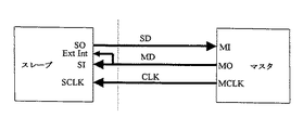
図5では、どのようにマスタとスレーブ装置の入力/出力へ、3つのバスラインを接続することができるかを示す。この例では、バスラインSDは、スレーブ装置のSOピンとマスタ装置のMIピンにに接続される。バスラインCLKはスレーブ装置のSCLKピンとマスタ装置のMCLKピンへ接続される。バスラインMDは、スレーブ装置のSIピンに接続され且つマスタ装置のMOピンに接続される。更に、バスラインMDは、スレーブ装置の外部割り込み入力Ext Intに接続される。スレーブの外部割り込み入力を伴なうバスラインMDの接続は、バスラインMD上の立下りエッジへのスレーブ装置の即時の応答が要求される、アービトレーションフェーズのために有利である。上述のようにマスタはアービトレーションフェーズで常に勝つので、そのような即時応答は、マスタ装置では要求されない。スレーブの外部割り込み入力とバスラインMDの接続は、代わりとして、スレーブ装置の内部でなされ得る。好ましい実施例では、図5に示すように、バスラインは単一方向であるが、しかし、バスラインCLKは、開発エンジニアの嗜好により変更することもできる。図示された場合では、クロック信号CLKはマスタから独占的に両方向に対して設けられる。しかし、これは、アプリケーションに依存し、そして、スレーブからマスタでも良い。
【0032】
図6では、どのようにマスタとスレーブ装置の入力へ、3つのバスラインを接続することができるかを示す。この実施例では、バスラインSDは更に、ラインSD上のエッジ信号の高速な応答のために、マスタの外部割り込み入力Ext Intへ接続される。
【0033】
代わりの実施例では、バスラインは双方向でも良い。
【0034】
新たなバスプロトコルで、2つの電子的構成要素間のデータ伝送は、非常に高速に、3つのバスラインを介して両方向になされることができる。上述の例では、1ms以下で16ビットデータ伝送が行われる。もちろん上述の表内にある値は、更に高速なデータ伝送が可能なように、実施に対応して変更を受け得る。
【0035】
【発明の効果】
本発明によって、バスラインの数を増加せずにより高いデータ伝送レートを達成できる、変更されたバスプロトコルを提供できる。
【図面の簡単な説明】
【図1】スレーブからマスタへのデータの伝送の信号を示す図である。
【図2】マスタからスレーブへのデータの伝送の信号を示す図である。
【図3】マスタからスレーブへの幾つかのデータ伝送を示す信号図である。
【図4】データビットの伝送のためのセットアップ時間とホールド時間機関を示す信号図である。
【図5】どのようにマスタとスレーブ装置の入力へバスラインを接続するかについての第1の例を示す図である。
【図6】どのようにマスタとスレーブ装置の入力へバスラインを接続するかについての第2の例を示す図である。
【符号の説明】
SD スレーブデータ
MD マスタデータ
CLK バスライン[0001]
BACKGROUND OF THE INVENTION
The present invention relates to a method for serial transmission of data between two electronic bus stations and to a bus station used in said method.
[0002]
[Prior art]
Consumer electronic products are often divided into two parts. These are the front end and the back end. Examples of consumer electronic products with this type of structure include all types of disc players, such as CD players (compact discs), MD players (mini discs), DVD players (digital multipurpose discs), and video CD players. And all its derivatives such as CD recorders. At the front end, user commands are received via keystrokes or remote controls. The instructions are sent to the backend section where they are executed to perform the associated control actions. The two part structure with front end and back end has the advantage that both parts can be developed independently of each other. Of course, an interface between the two parts is necessary. This interface can be used in a variety of applications.
[0003]
A known interface for data exchange between two electronic devices is the “Video 6001 DSA Interface 7003” from Philips. It is a serial bus interface that provides serial transmission of data between two electronic components. By way of example, within each electronic device is an interface electronic circuit that is internally connected to an internal address, data and control bus and externally connected to a serial bus connection bus line. Three data buses are required for serial data transmission according to the Philips DSA bus description. One line is dedicated to the data signal, the second line is reserved for control, the second line is STB, and the third line is SCK. In particular, these lines are used for handshaking signals. If the transmitter wants to send some data, it first clears the data line to indicate that it wants to send data. Then, it waits for the ACK line set by the receiver to become low level. After this, the transmitter sets the data line high and then waits for the ACK line from the receiver to go high, signaling the end of synchronization start.
[0004]
After this, the transmitter transmits data to the receiver via the DATA line. Data is transmitted in units of 16-bit data words for each transmission phase. The transmitter sets the data line according to the bit to be transmitted. When the DATA line becomes stable, the transmitter clears the STB line to inform the receiver that the information on the DATA line is valid. The receiver reads the DATA line after recognizing that the STB line is low. The receiver then clears the ACK line and informs the transmitter that the bit has been read. The transmitter sets the STB line high and waits for the ACK line to go high. When the ACK line goes high, one data bit is completely transmitted.
[0005]
[Problems to be solved by the invention]
As described above, in the Philips DSA bus protocol, each data bit of the data transmission is declared valid and is notified by handshake signals on the STB and ACK lines. This is the first reason for relatively slow bus transmission. Furthermore, a relatively long synchronization start process needs to be performed for each 16-bit data transmission. This is the second reason for reducing the data transmission rate.
[0006]
After recognizing these disadvantages, it is an object of the present invention to provide a modified bus protocol that can achieve higher data transmission rates without increasing the number of bus lines.
[0007]
[Means for Solving the Problems]
This object is achieved with the solution defined in the independent claim 1. The new bus protocol according to the invention is based on a combination of asynchronous and synchronous data transmission. The bits of the data word are transmitted synchronously from the transmitter to the receiver. This means that there is no handshake signal associated with the transmission of each bit. Instead, the transmitter / receiver generates a data transmission clock that is transmitted in parallel on a dedicated bus line. Thereby, the sampling point for the receiver is predefined by this clock signal, as is well known in the known synchronous serial transmission mode. With this type of synchronous data transmission, very high data transmission rates can be achieved.
[0008]
The bus protocol stipulates that data transmission from a master to a slave is notified by sending an edge signal on a bus line configured to be a data line for the master. The other bus lines are configured to be control lines for transmission from the master to the slave. For data transmission from the slave to the master, different bus lines are configured as slave data lines, and the other bus lines are configured as control lines for transmission from the slave to the master. There is a dedicated bus line that carries the clock signal. This is valid in both transmission directions, depending on the application, from master to slave and vice versa. With this bus line configuration, bus contention when two bus stations attempt to access the bus at the same time can be easily resolved during transmission without the need for repeated transmission.
[0009]
In such a case, a dedicated start edge signal is transmitted to both stations on different bus lines, so that the master always wins this contention, and the slave has time associated with the start edge signal from the master. During the period, changing the state to receive mode is easily achieved. The master then synchronizes itself to the edge signal on the control line activated by the slave, thereby causing synchronous data transmission. A relatively short fixed delay for selecting the correct phase of the clock signal generated within the transmitter / receiver because the reconfiguration has already taken place during the start bit time period It is possible to define the time. After this time period, data transmission via the data line and the clock line is started.
[0010]
Advantageously, further embodiments of the invention are disclosed in the dependent claims.
[0011]
Data transmission in the direction from the master to the slave can be easily performed in the same manner as the data transmission from the slave to the master with reference to
[0012]
If an 8-bit microcontroller is used for the bus station, transmission of a 16-bit data word in two parts from the master to the slave or vice versa is advantageous. Since the internal data bus is only 8 bits, 16-bit data requires two different bus periods to be transmitted to the memory. Another advantage is that certain byte handshakes ensure that each byte is transmitted correctly. For example, if an error occurs in the first transmission phase, the data transmission can be interrupted immediately, whereby the data transmission can be repeated at a high speed.
[0013]
As for the bus station used in the method according to the present invention, in order to guarantee an instantaneous response to the start edge signal sent from another bus station, in addition to the data input, to the external interrupt input, the bus dedicated to the data signal It is advantageous to connect the lines. This is particularly advantageous for slave stations. By doing so, bus contention is resolved immediately within the transmission without having to wait for the transmission to be aborted and repeated.
[0014]
DETAILED DESCRIPTION OF THE INVENTION
The bus protocol according to the present invention is illustrated by two examples.
[0015]
First, data transmission from the slave device to the master device will be described. FIG. 1 shows signals on three bus lines for data transmission operations. Prior to data transmission, all three bus lines are placed in an idle state, which in this example is a “high” state. Of course, in other embodiments, the idle state may be a “low” state on the bus line, and the activated state may be a “high” state. Data transmission from the slave to the master is started by transmitting an edge signal from the slave to the master via the bus line SD. Here, SD means “slave data”. In order to transmit an edge signal, the bus line SD is activated. Next, the time period Tm. followed by sync. The master device detects the edge signal on the bus line SD and reacts accordingly. In particular, the reception mode is entered in response to detection of the start bit. This means that it is in the reception mode during the next data transmission period, and the bus is not accessed even if a transmission request is received from the application microcontroller. After the master device is ready for the reception mode, the master device sets the bus line MD from idle to an activated state. Here, MD means master data. The edge signal thus generated informs the slave that the master is already in the receiving state. There is a characteristic time period T1 after the edge signal on the bus line MD, where the master selects the correct phase of the free-running clock signal for internally generated data transmission. This can be done with a controllable delay line that receives a free-run clock signal as input, and the edge signal on the bus line MD is used as a reference. An example of such a controllable delay line is disclosed in EP-A-0303494. Reference is made in particular to this document for an explanation of this controllable delay line. In this embodiment, the master generates the clock signal, and the slave that is the transmitter does not. The clock signal is thus supplied by the receiver.
[0016]
The clock signal is generated on the data line CLK with the correct phase after the time T1 has elapsed. At the start of the clock signal, the first data bit H7 is set on the bus line SD. Each bit is evaluated in the master at the rising edge of the transmitted clock. This operation is repeated for each of the 8 bits from H7 to H0 in the first transmission phase. After transmission of bit H0, the first transmission phase ends with a timeout period T5. The bus line CLK is set to an idle state during this period. This gives the master device time to transfer data from the 8-bit receive shift register to the memory.
[0017]
The second transmission phase of the data transmission operation starts at the rising edge of the bus line MD. Thus, for the second phase, the master device sets an idle state on the bus line MD. By doing so, the master device informs the slave device that the preparation for receiving the second data byte is completed. After the elapse of time period T6 from the rising edge on the bus line MD, the clock signal and the first bit of the second transmission phase are generated on the bus lines CLK and SD. The time period T6 can be a very short time period compared to the time period T1. During this time period, the resynchronization of the free-run clock signal takes place with the controllable delay line described above.
[0018]
Bits A7 to A0 are transmitted via the bus line SD in synchronization with the clock signal. Bit evaluation is performed at each rising edge of the clock signal in each case. After the last bit A0 is evaluated, data transmission is stopped and all data lines are idle. Time period T7 indicates the last hold time of bit A0.
[0019]
Note that FIG. 1 is not drawn to scale and therefore the duration of the time period cannot be directly compared in FIG. For this purpose, a table of exact values for different time periods is given later in this description.
[0020]
Next, data transmission from the master device to the slave device will be described. For this purpose, reference is made to FIG. Components identical to those in FIG. 1 are given the same reference symbols. The major difference from FIG. 1 is that the bus line MD is used for the transmission of data bits from the master to the slave, and the bus line SD is used for indication and synchronization of the transmission phase. The bus line CLK is again used to send a clock from the master to the slave.
[0021]
The other difference is the time period Ts. sync is the time period Tm. It has a length different from sync. Time period Ts. The sync is advantageous for avoiding bus contention when both the master and slave devices simultaneously access the bus line, as will be described later. It is defined to be shorter than sync.
[0022]
The time period T2 in FIG. 2 is slightly different from the corresponding time period T1. However, in other embodiments, it may be the same as the time period T1. This difference is therefore not relevant for the description of the invention.
[0023]
Data transmission from the master to the slave is also performed in two phases of 8 data bits after resynchronization of each phase and the first phase. For this purpose, reference is made to FIG.
[0024]
Next, the case where both bus stations are performing arbitration for bus access will be described in more detail. Since there are only two bus stations, the conflict is resolved relatively easily. The master indicates the intention of bus access by sending an edge signal on the bus line MD. The slave indicates the intention to access the bus by sending an edge signal on the bus line SD. The master is defined to dominate and therefore wins the arbitration phase. This is ensured by specifying that the slave monitors the bus line MD when it sends a start bit via the bus line SD. If the slave has a minimum synchronization time period Tm. sync, Ts. When the activation state on the bus line MD is detected during sync (10 μsec in the following table example), the data transmission is stopped, and the reception mode is immediately set again. This task is Ts. There is no need to interrupt the data transmission from the master to the slave, which takes place within the sync. Therefore, the bus contention is the time period Ts. Resolved within sync.
Since the master dominates the slave device and is not interrupted, the master does not need to monitor the bus line SD within this minimum time period.
[0025]
Time period Tm. sync is Ts. The specification longer than sync ensures that the bus line MD is not driven by the slave device before bus contention is resolved. This avoids hardware failure due to bus line overload.
[0026]
FIG. 3 shows several consecutive data transmissions from the master to the slave. Indicates that there is a timeout between the two transmissions. The corresponding time period has the reference symbol Ttimeout. This timeout ensures that the receiver writes the latest received data into memory and the receive shift register is cleared for the next transmission. A similar operation needs to be performed at the transmitter. Here, the transmission shift register is cleared and requires the next 8-bit data word to be loaded into the transmission shift register. Of course, reloading of the transmission shift register only takes place when a transmission request has already been received from the application microcontroller. If the master does not want to transmit data, the transmission shift register is not reloaded, but the receive shift register is cleared in preparation for possible data transmission from the slave to the master. I need. Thus, the transmission shift register needs to be loaded during this time period when received in the slave bus interface device.
[0027]
One possible modification for other embodiments is to provide only one 8-bit register within each bus station. Here, the output of each shift register needs to be switched from one bus line to another during reconfiguration from the reception mode to the transmission mode or vice versa. Accordingly, the corresponding control logic needs to be executed.
[0028]
FIG. 4 shows the setup time and hold time of data bit transmission related to the clock signal.
[0029]
The following table shows typical values and tolerances for the various time periods described above and shown in the figures.
[0030]
[Table 2]
[0031]
FIG. 5 shows how three bus lines can be connected to the inputs / outputs of the master and slave devices. In this example, the bus line SD is connected to the SO pin of the slave device and the MI pin of the master device. The bus line CLK is connected to the SCLK pin of the slave device and the MCLK pin of the master device. The bus line MD is connected to the SI pin of the slave device and to the MO pin of the master device. Further, the bus line MD is connected to the external interrupt input Ext Int of the slave device. Connection of the bus line MD with the slave's external interrupt input is advantageous for the arbitration phase, where an immediate response of the slave device to the falling edge on the bus line MD is required. As mentioned above, since the master always wins in the arbitration phase, such an immediate response is not required at the master device. The connection between the slave external interrupt input and the bus line MD can alternatively be made inside the slave device. In the preferred embodiment, the bus line is unidirectional, as shown in FIG. 5, but the bus line CLK can be changed according to the preference of the development engineer. In the illustrated case, the clock signal CLK is provided exclusively in both directions from the master. However, this is application dependent and can be slave to master.
[0032]
FIG. 6 shows how three bus lines can be connected to the inputs of the master and slave devices. In this embodiment, the bus line SD is further connected to the master's external interrupt input Ext Int for fast response of edge signals on the line SD.
[0033]
In an alternative embodiment, the bus line may be bidirectional.
[0034]
With the new bus protocol, data transmission between two electronic components can be done in both directions via three bus lines at very high speed. In the above example, 16-bit data transmission is performed in 1 ms or less. Of course, the values in the above table can be modified according to implementation so that higher speed data transmission is possible.
[0035]
【The invention's effect】
The present invention can provide a modified bus protocol that can achieve a higher data transmission rate without increasing the number of bus lines.
[Brief description of the drawings]
FIG. 1 is a diagram illustrating a signal for data transmission from a slave to a master.
FIG. 2 is a diagram illustrating a signal for data transmission from a master to a slave.
FIG. 3 is a signal diagram illustrating several data transmissions from a master to a slave.
FIG. 4 is a signal diagram illustrating a setup time and hold time engine for transmission of data bits.
FIG. 5 is a diagram showing a first example of how to connect a bus line to inputs of a master and a slave device.
FIG. 6 is a diagram showing a second example of how to connect a bus line to inputs of a master and a slave device.
[Explanation of symbols]
SD Slave data MD Master data CLK Bus line
Claims (9)
(i)送信局(SLAVE)から受信局(MASTER)へ、前記第2のライン(SD)上で、第1の方向へ第1のエッジ信号を送信することによりデータ伝送を開始するステップと、
(ii)第1のエッジ信号に応答して、前記第1のエッジ信号の発生から第1の量の時間(Tm.sync)の経過後に、第3のライン(MD)をアイドル状態から活性化状態へ切換えるステップと、
(iii)第3のライン(MD)の活性化状態の発生から第2の量の時間(T1)の経過後に、前記第2と第1のライン(SD,CLK)を介して同期データ伝送を開始するステップとを有する方法。The first line (CLK) is dedicated to the clock signal and the second and third lines (SD, MD) are dedicated to the data signal or the control signal, two electronic via a three-line bus connection A method for serial transmission of data between bus stations,
(I) starting data transmission by transmitting a first edge signal in a first direction on the second line (SD) from a transmitting station (SLAVE) to a receiving station (MASTER);
(Ii) In response to the first edge signal, the third line (MD) is activated from the idle state after a first amount of time (Tm.sync) has elapsed since the generation of the first edge signal. A step to switch to a state;
(Iii) Synchronous data transmission via the second and first lines (SD, CLK) after a second amount of time (T1) has elapsed since the activation of the third line (MD). And a step of starting.
(i)前記第3のライン(MD)上で、送信局(MASTER)から受信局(SLAVE)へ、第2のエッジ信号を送信するステップと、
(ii)第2のエッジ信号に応答して、前記第2のエッジ信号の発生から第3の量の時間(Ts.sync)の経過後に、第2のライン(SD)をアイドル状態から活性化状態へ切換えるステップと、
(iii)第2のライン(SD)の活性化状態の発生から第4の量の時間(T2)の経過後に、前記第2と第1のライン(MD,CLK)を介して同期データ伝送を開始するステップにより行われる請求項1に記載の方法。The data transmission in the second direction opposite to the first direction is as follows:
(I) transmitting a second edge signal from the transmitting station (MASTER) to the receiving station (SLAVE) on the third line (MD);
(Ii) In response to the second edge signal, the second line (SD) is activated from the idle state after a third amount of time (Ts.sync) has elapsed since the generation of the second edge signal. A step to switch to a state;
(Iii) After a fourth amount of time (T2) has elapsed since the activation of the second line (SD), the synchronous data transmission is performed via the second and first lines (MD, CLK). The method of claim 1, wherein the method is performed by an initiating step.
Applications Claiming Priority (2)
| Application Number | Priority Date | Filing Date | Title |
|---|---|---|---|
| EP00250058.5 | 2000-02-22 | ||
| EP00250058A EP1128271A1 (en) | 2000-02-22 | 2000-02-22 | Method for the serial transfer of data between two electronic bus stations and bus station for use in said method |
Publications (2)
| Publication Number | Publication Date |
|---|---|
| JP2001274862A JP2001274862A (en) | 2001-10-05 |
| JP4565459B2 true JP4565459B2 (en) | 2010-10-20 |
Family
ID=8172592
Family Applications (1)
| Application Number | Title | Priority Date | Filing Date |
|---|---|---|---|
| JP2001034866A Expired - Fee Related JP4565459B2 (en) | 2000-02-22 | 2001-02-13 | Method for serial transmission of data between two electronic bus stations and bus station used in the method |
Country Status (7)
| Country | Link |
|---|---|
| US (1) | US6763413B2 (en) |
| EP (1) | EP1128271A1 (en) |
| JP (1) | JP4565459B2 (en) |
| CN (1) | CN1170234C (en) |
| DE (1) | DE60119805T2 (en) |
| HK (1) | HK1037755A1 (en) |
| TW (1) | TWI220828B (en) |
Families Citing this family (20)
| Publication number | Priority date | Publication date | Assignee | Title |
|---|---|---|---|---|
| US7594026B1 (en) * | 2001-04-25 | 2009-09-22 | Zarlink Semiconductor (U.S.) Inc. | Method and apparatus for multi-phy communication without an ATM bus master |
| JP2002351825A (en) * | 2001-05-29 | 2002-12-06 | Rohm Co Ltd | Communication system |
| ES2238665T3 (en) * | 2003-03-11 | 2005-09-01 | Alcatel | SYSTEM FOR AUTOMATICALLY CONFIGURING A TRANSCEIVER AS A CENTRAL UNIT OR A REMOTE UNIT, IN A COMMUNICATIONS SYSTEM. |
| US20040200896A1 (en) * | 2003-04-14 | 2004-10-14 | Marcus Eckerl | Apparatus for storing and transferring personal data |
| JP2005301963A (en) * | 2003-07-08 | 2005-10-27 | Ricoh Co Ltd | Data transfer device, image forming device, data transfer method, computer program and recording medium |
| US7308516B2 (en) * | 2004-04-26 | 2007-12-11 | Atmel Corporation | Bi-directional serial interface for communication control |
| US9047415B2 (en) | 2005-06-10 | 2015-06-02 | Freescale Semiconductor, Inc. | Device and method for media access control |
| WO2006131142A1 (en) | 2005-06-10 | 2006-12-14 | Freescale Semiconductor, Inc. | Method and device for frame synchronization |
| WO2007063482A2 (en) * | 2005-11-29 | 2007-06-07 | Nxp B.V. | Bus station and system and method of maintaining synchronizing of a bus station |
| JP4759494B2 (en) * | 2006-11-13 | 2011-08-31 | パナソニック株式会社 | Serial data communication system and serial data communication device |
| CN101296405B (en) * | 2007-04-25 | 2012-05-09 | 中兴通讯股份有限公司 | Method for wireless communication of main unit to multiple mobile terminals |
| JP5241625B2 (en) * | 2009-06-15 | 2013-07-17 | ルネサスエレクトロニクス株式会社 | Serial communication system |
| CN102147778B (en) * | 2010-02-05 | 2013-09-11 | 杭州华三通信技术有限公司 | Data transmission system based on half-duplex serial bus and transmission control method |
| US8959268B2 (en) * | 2012-03-09 | 2015-02-17 | Canon Kabushiki Kaisha | Information processing apparatus, serial communication system, method of initialization of communication therefor and serial communication apparatus |
| CN104350700B (en) * | 2012-05-29 | 2017-05-31 | 飞思卡尔半导体公司 | For the clock of serial communication device |
| JP6201890B2 (en) * | 2014-05-16 | 2017-09-27 | 株式会社デンソー | Slave communication device and bus communication system |
| JP2017063375A (en) * | 2015-09-25 | 2017-03-30 | 富士ゼロックス株式会社 | Data communication control device, image reading device and image formation device |
| GB2555601A (en) * | 2016-11-02 | 2018-05-09 | Roli Ltd | Data flow control |
| US10606794B1 (en) * | 2019-05-14 | 2020-03-31 | Infineon Technologies Ag | Clock signal monitor for slave device on a master-slave bus |
| US10958412B1 (en) | 2020-01-22 | 2021-03-23 | Infineon Technologies Ag | Communication using edge timing in a signal |
Citations (4)
| Publication number | Priority date | Publication date | Assignee | Title |
|---|---|---|---|---|
| JPH01205647A (en) * | 1988-02-12 | 1989-08-18 | Nec Corp | Serial communication system |
| JPH06209348A (en) * | 1992-08-12 | 1994-07-26 | Philips Electron Nv | Multiplex station communication bus system |
| JPH10334044A (en) * | 1997-06-03 | 1998-12-18 | Oki Electric Ind Co Ltd | Serial interface method |
| JPH11234364A (en) * | 1998-02-18 | 1999-08-27 | Fuji Xerox Co Ltd | Communication control method and communication module |
Family Cites Families (8)
| Publication number | Priority date | Publication date | Assignee | Title |
|---|---|---|---|---|
| US4369516A (en) * | 1980-09-15 | 1983-01-18 | Motorola, Inc. | Self-clocking data transmission system |
| US4654655A (en) * | 1984-03-02 | 1987-03-31 | Motorola, Inc. | Multi-user serial data bus |
| JPS6280755A (en) * | 1985-10-04 | 1987-04-14 | Minolta Camera Co Ltd | Data transmission control system |
| US5146567A (en) * | 1989-08-22 | 1992-09-08 | Acer Incorporated | Keyboard interface |
| EP0589499B1 (en) * | 1992-08-12 | 1999-04-07 | Koninklijke Philips Electronics N.V. | A multistation communication bus system, and a master station and a slave station for use in such system |
| US5758098A (en) * | 1994-05-12 | 1998-05-26 | Apple Computer, Inc. | Method and apparatus for providing a high throughput two-conductor serial interface with support for slave device detection |
| DE69515147T2 (en) * | 1994-07-15 | 2000-09-21 | Thomson Consumer Electronics | Multiple protocol data bus system |
| US5848072A (en) * | 1995-08-10 | 1998-12-08 | Motorola, Inc. | Method of and apparatus for communicating messages |
-
2000
- 2000-02-22 EP EP00250058A patent/EP1128271A1/en not_active Withdrawn
-
2001
- 2001-01-19 TW TW090101225A patent/TWI220828B/en not_active IP Right Cessation
- 2001-02-09 DE DE60119805T patent/DE60119805T2/en not_active Expired - Lifetime
- 2001-02-12 CN CNB011037288A patent/CN1170234C/en not_active Expired - Fee Related
- 2001-02-13 JP JP2001034866A patent/JP4565459B2/en not_active Expired - Fee Related
- 2001-02-21 US US09/790,121 patent/US6763413B2/en not_active Expired - Lifetime
- 2001-12-05 HK HK01108528A patent/HK1037755A1/en not_active IP Right Cessation
Patent Citations (4)
| Publication number | Priority date | Publication date | Assignee | Title |
|---|---|---|---|---|
| JPH01205647A (en) * | 1988-02-12 | 1989-08-18 | Nec Corp | Serial communication system |
| JPH06209348A (en) * | 1992-08-12 | 1994-07-26 | Philips Electron Nv | Multiplex station communication bus system |
| JPH10334044A (en) * | 1997-06-03 | 1998-12-18 | Oki Electric Ind Co Ltd | Serial interface method |
| JPH11234364A (en) * | 1998-02-18 | 1999-08-27 | Fuji Xerox Co Ltd | Communication control method and communication module |
Also Published As
| Publication number | Publication date |
|---|---|
| JP2001274862A (en) | 2001-10-05 |
| DE60119805D1 (en) | 2006-06-29 |
| EP1128271A1 (en) | 2001-08-29 |
| US6763413B2 (en) | 2004-07-13 |
| HK1037755A1 (en) | 2002-02-15 |
| DE60119805T2 (en) | 2006-10-12 |
| US20010023468A1 (en) | 2001-09-20 |
| TWI220828B (en) | 2004-09-01 |
| CN1170234C (en) | 2004-10-06 |
| CN1310403A (en) | 2001-08-29 |
Similar Documents
| Publication | Publication Date | Title |
|---|---|---|
| JP4565459B2 (en) | Method for serial transmission of data between two electronic bus stations and bus station used in the method | |
| KR102445344B1 (en) | Receive clock calibration for a serial bus | |
| US7328399B2 (en) | Synchronous serial data communication bus | |
| JP6061868B2 (en) | Serial interface | |
| KR20030033040A (en) | Generalized i2c slave transmitter/receiver state machine | |
| EP0522763B1 (en) | High performance asynchronous bus interface | |
| JP2002232508A (en) | Electronic device and method for automatically selecting interface protocol used by the electronic device | |
| US20060277339A1 (en) | Communication apparatus, switching method, and switching program | |
| JPH06324977A (en) | Data transfer method | |
| US6170027B1 (en) | LPC/ISA bridge and its bridging method | |
| JP4160068B2 (en) | Digital programming interface between baseband processor and radio frequency integrated module | |
| CN111221769A (en) | Single wire read-write communication method | |
| CN116126771A (en) | Communication system and method for two-wire SPI | |
| EP1128272B1 (en) | Method for the serial transfer of data between two electronic bus stations and bus station for use in said method | |
| Jyothi et al. | Implementation of SPI Communication Protocol for Multipurpose Applications with I2C Power and Area Reduction | |
| JP2958601B2 (en) | Data communication method | |
| KR100266963B1 (en) | Method and apparatus for reducing latency rime on an interface by overlapping transmitted packets | |
| TWI818834B (en) | Microcontroller and serial peripheral interface system using the same | |
| JP4290412B2 (en) | Data transfer device | |
| US20030053573A1 (en) | Microcontroller having a transmission-bus-interface | |
| JP3580763B2 (en) | Data transceiver | |
| KR0184402B1 (en) | Interrupt generating apparatus for i bus | |
| JP4140753B2 (en) | Synchronous data transmission method | |
| KR100295683B1 (en) | General call acknowledge apparatus and method for inter-integrated circuit | |
| CN117033292A (en) | I based on APB bus control 2 C interrupt method |
Legal Events
| Date | Code | Title | Description |
|---|---|---|---|
| A621 | Written request for application examination |
Free format text: JAPANESE INTERMEDIATE CODE: A621 Effective date: 20080212 |
|
| A977 | Report on retrieval |
Free format text: JAPANESE INTERMEDIATE CODE: A971007 Effective date: 20100623 |
|
| TRDD | Decision of grant or rejection written | ||
| A01 | Written decision to grant a patent or to grant a registration (utility model) |
Free format text: JAPANESE INTERMEDIATE CODE: A01 Effective date: 20100629 |
|
| A01 | Written decision to grant a patent or to grant a registration (utility model) |
Free format text: JAPANESE INTERMEDIATE CODE: A01 |
|
| A61 | First payment of annual fees (during grant procedure) |
Free format text: JAPANESE INTERMEDIATE CODE: A61 Effective date: 20100728 |
|
| R150 | Certificate of patent or registration of utility model |
Free format text: JAPANESE INTERMEDIATE CODE: R150 |
|
| FPAY | Renewal fee payment (event date is renewal date of database) |
Free format text: PAYMENT UNTIL: 20130813 Year of fee payment: 3 |
|
| R250 | Receipt of annual fees |
Free format text: JAPANESE INTERMEDIATE CODE: R250 |
|
| LAPS | Cancellation because of no payment of annual fees |