JP4550160B2 - Compound for organic electroluminescent device and organic electroluminescent device - Google Patents
Compound for organic electroluminescent device and organic electroluminescent device Download PDFInfo
- Publication number
- JP4550160B2 JP4550160B2 JP2009516335A JP2009516335A JP4550160B2 JP 4550160 B2 JP4550160 B2 JP 4550160B2 JP 2009516335 A JP2009516335 A JP 2009516335A JP 2009516335 A JP2009516335 A JP 2009516335A JP 4550160 B2 JP4550160 B2 JP 4550160B2
- Authority
- JP
- Japan
- Prior art keywords
- group
- organic electroluminescent
- light emitting
- ring
- compound
- Prior art date
- Legal status (The legal status is an assumption and is not a legal conclusion. Google has not performed a legal analysis and makes no representation as to the accuracy of the status listed.)
- Active
Links
- 0 C*(C(C=C1)=CC(C=C2)=*(C)C2=C(C(*2)=CC[C@]2C=C2*([*+])=C3C=C2)C2=CC=CCC2C)C1=C3C1=CCC(C)C=C1 Chemical compound C*(C(C=C1)=CC(C=C2)=*(C)C2=C(C(*2)=CC[C@]2C=C2*([*+])=C3C=C2)C2=CC=CCC2C)C1=C3C1=CCC(C)C=C1 0.000 description 2
Images

Classifications
-
- C—CHEMISTRY; METALLURGY
- C07—ORGANIC CHEMISTRY
- C07D—HETEROCYCLIC COMPOUNDS
- C07D487/00—Heterocyclic compounds containing nitrogen atoms as the only ring hetero atoms in the condensed system, not provided for by groups C07D451/00 - C07D477/00
- C07D487/02—Heterocyclic compounds containing nitrogen atoms as the only ring hetero atoms in the condensed system, not provided for by groups C07D451/00 - C07D477/00 in which the condensed system contains two hetero rings
- C07D487/04—Ortho-condensed systems
-
- C—CHEMISTRY; METALLURGY
- C09—DYES; PAINTS; POLISHES; NATURAL RESINS; ADHESIVES; COMPOSITIONS NOT OTHERWISE PROVIDED FOR; APPLICATIONS OF MATERIALS NOT OTHERWISE PROVIDED FOR
- C09K—MATERIALS FOR MISCELLANEOUS APPLICATIONS, NOT PROVIDED FOR ELSEWHERE
- C09K11/00—Luminescent, e.g. electroluminescent, chemiluminescent materials
- C09K11/06—Luminescent, e.g. electroluminescent, chemiluminescent materials containing organic luminescent materials
-
- H—ELECTRICITY
- H10—SEMICONDUCTOR DEVICES; ELECTRIC SOLID-STATE DEVICES NOT OTHERWISE PROVIDED FOR
- H10K—ORGANIC ELECTRIC SOLID-STATE DEVICES
- H10K50/00—Organic light-emitting devices
-
- H—ELECTRICITY
- H10—SEMICONDUCTOR DEVICES; ELECTRIC SOLID-STATE DEVICES NOT OTHERWISE PROVIDED FOR
- H10K—ORGANIC ELECTRIC SOLID-STATE DEVICES
- H10K85/00—Organic materials used in the body or electrodes of devices covered by this subclass
- H10K85/60—Organic compounds having low molecular weight
- H10K85/649—Aromatic compounds comprising a hetero atom
- H10K85/654—Aromatic compounds comprising a hetero atom comprising only nitrogen as heteroatom
-
- H—ELECTRICITY
- H10—SEMICONDUCTOR DEVICES; ELECTRIC SOLID-STATE DEVICES NOT OTHERWISE PROVIDED FOR
- H10K—ORGANIC ELECTRIC SOLID-STATE DEVICES
- H10K85/00—Organic materials used in the body or electrodes of devices covered by this subclass
- H10K85/60—Organic compounds having low molecular weight
- H10K85/649—Aromatic compounds comprising a hetero atom
- H10K85/657—Polycyclic condensed heteroaromatic hydrocarbons
- H10K85/6572—Polycyclic condensed heteroaromatic hydrocarbons comprising only nitrogen in the heteroaromatic polycondensed ring system, e.g. phenanthroline or carbazole
-
- C—CHEMISTRY; METALLURGY
- C09—DYES; PAINTS; POLISHES; NATURAL RESINS; ADHESIVES; COMPOSITIONS NOT OTHERWISE PROVIDED FOR; APPLICATIONS OF MATERIALS NOT OTHERWISE PROVIDED FOR
- C09K—MATERIALS FOR MISCELLANEOUS APPLICATIONS, NOT PROVIDED FOR ELSEWHERE
- C09K2211/00—Chemical nature of organic luminescent or tenebrescent compounds
- C09K2211/10—Non-macromolecular compounds
- C09K2211/1018—Heterocyclic compounds
- C09K2211/1025—Heterocyclic compounds characterised by ligands
- C09K2211/1029—Heterocyclic compounds characterised by ligands containing one nitrogen atom as the heteroatom
-
- C—CHEMISTRY; METALLURGY
- C09—DYES; PAINTS; POLISHES; NATURAL RESINS; ADHESIVES; COMPOSITIONS NOT OTHERWISE PROVIDED FOR; APPLICATIONS OF MATERIALS NOT OTHERWISE PROVIDED FOR
- C09K—MATERIALS FOR MISCELLANEOUS APPLICATIONS, NOT PROVIDED FOR ELSEWHERE
- C09K2211/00—Chemical nature of organic luminescent or tenebrescent compounds
- C09K2211/18—Metal complexes
- C09K2211/185—Metal complexes of the platinum group, i.e. Os, Ir, Pt, Ru, Rh or Pd
-
- H—ELECTRICITY
- H10—SEMICONDUCTOR DEVICES; ELECTRIC SOLID-STATE DEVICES NOT OTHERWISE PROVIDED FOR
- H10K—ORGANIC ELECTRIC SOLID-STATE DEVICES
- H10K50/00—Organic light-emitting devices
- H10K50/10—OLEDs or polymer light-emitting diodes [PLED]
- H10K50/11—OLEDs or polymer light-emitting diodes [PLED] characterised by the electroluminescent [EL] layers
-
- H—ELECTRICITY
- H10—SEMICONDUCTOR DEVICES; ELECTRIC SOLID-STATE DEVICES NOT OTHERWISE PROVIDED FOR
- H10K—ORGANIC ELECTRIC SOLID-STATE DEVICES
- H10K85/00—Organic materials used in the body or electrodes of devices covered by this subclass
- H10K85/30—Coordination compounds
- H10K85/341—Transition metal complexes, e.g. Ru(II)polypyridine complexes
- H10K85/342—Transition metal complexes, e.g. Ru(II)polypyridine complexes comprising iridium
-
- H—ELECTRICITY
- H10—SEMICONDUCTOR DEVICES; ELECTRIC SOLID-STATE DEVICES NOT OTHERWISE PROVIDED FOR
- H10K—ORGANIC ELECTRIC SOLID-STATE DEVICES
- H10K85/00—Organic materials used in the body or electrodes of devices covered by this subclass
- H10K85/30—Coordination compounds
- H10K85/341—Transition metal complexes, e.g. Ru(II)polypyridine complexes
- H10K85/346—Transition metal complexes, e.g. Ru(II)polypyridine complexes comprising platinum
-
- H—ELECTRICITY
- H10—SEMICONDUCTOR DEVICES; ELECTRIC SOLID-STATE DEVICES NOT OTHERWISE PROVIDED FOR
- H10K—ORGANIC ELECTRIC SOLID-STATE DEVICES
- H10K85/00—Organic materials used in the body or electrodes of devices covered by this subclass
- H10K85/60—Organic compounds having low molecular weight
- H10K85/615—Polycyclic condensed aromatic hydrocarbons, e.g. anthracene
- H10K85/626—Polycyclic condensed aromatic hydrocarbons, e.g. anthracene containing more than one polycyclic condensed aromatic rings, e.g. bis-anthracene
Description
本発明は新規な有機電界発光素子用化合物及び有機電界発光素子(以下、有機EL素子という)に関するものであり、詳しくは、燐光発光ドーパントと特定の構造を有するホスト化合物を併用することにより、高輝度を示す有機EL素子に関するものである。 The present invention relates to a novel compound for an organic electroluminescent device and an organic electroluminescent device (hereinafter referred to as an organic EL device), and more specifically, by combining a phosphorescent dopant and a host compound having a specific structure, The present invention relates to an organic EL element exhibiting luminance.
一般に、有機EL素子は、その最も簡単な構造としては発光層及び該層を挟んだ一対の対向電極から構成されている。すなわち、有機EL素子では、両電極間に電界が印加されると、陰極から電子が注入され、陽極から正孔が注入され、これらが発光層において再結合エネルギー準位が伝導帯から価電子帯に戻る際にエネルギーとして光を放出する現象を利用する。 In general, the organic EL element has a light emitting layer and a pair of counter electrodes sandwiching the layer as its simplest structure. That is, in an organic EL element, when an electric field is applied between both electrodes, electrons are injected from the cathode and holes are injected from the anode. These recombination energy levels in the light emitting layer change from the conduction band to the valence band. Utilizing the phenomenon of emitting light as energy when returning to.
近年、有機薄膜を用いたEL素子の開発が行われるようになった。特に発光効率を高めるため、電極からキャリアー注入の効率向上を目的として電極の種類の最適化を行い、芳香族ジアミンからなる正孔輸送層と8−ヒドロキシキノリンアルミニウム錯体(以下、Alq3という)からなる発光層とを電極間に薄膜として設けた素子の開発により、従来のアントラセン等の単結晶を用いた素子と比較して大幅な発光効率の改善がなされたことから、自発光・高速応答性といった特徴を持つ高性能フラットパネルへの実用を目指して進められてきた。 In recent years, EL devices using organic thin films have been developed. In particular, in order to improve luminous efficiency, the type of electrode is optimized for the purpose of improving the efficiency of carrier injection from the electrode, and consists of a hole transport layer made of aromatic diamine and 8-hydroxyquinoline aluminum complex (hereinafter referred to as Alq3). The development of a device with a light emitting layer as a thin film between the electrodes has greatly improved the light emission efficiency compared to conventional devices using single crystals such as anthracene. It has been promoted aiming at practical application to high-performance flat panels with features.
また、素子の発光効率を上げる試みとして、蛍光ではなく燐光を用いることも検討されている。上記の芳香族ジアミンからなる正孔輸送層とAlq3からなる発光層とを設けた素子をはじめとした多くの素子が蛍光発光を利用したものであったが、燐光発光を用いる、すなわち、三重項励起状態からの発光を利用すれば、従来の蛍光(一重項)を用いた素子と比べて、3倍程度の効率向上が期待される。この目的のためにクマリン誘導体やベンゾフェノン誘導体を発光層とすることが検討されてきたが、極めて低い輝度しか得られなかった。その後、三重項状態を利用する試みとして、ユーロピウム錯体を用いることが検討されてきたが、これも高効率の発光には至らなかった。燐光発光ドーパントとしては、特許文献1に挙げられるような提案が多数行われている。
In addition, as an attempt to increase the light emission efficiency of the device, the use of phosphorescence instead of fluorescence has been studied. Many devices, including those provided with the hole transport layer composed of the above aromatic diamine and the light emitting layer composed of Alq3, used fluorescence emission, but use phosphorescence emission, that is, triplet. If light emission from an excited state is used, an efficiency improvement of about three times is expected compared to a conventional device using fluorescence (singlet). For this purpose, it has been studied to use a coumarin derivative or a benzophenone derivative as a light emitting layer, but only an extremely low luminance was obtained. Thereafter, the use of a europium complex has been studied as an attempt to utilize the triplet state, but this also did not lead to highly efficient light emission. As a phosphorescent dopant, many proposals such as those described in
有機EL素子開発において発光層に用いるホスト材料として提案されているのは、特許文献2で紹介されているカルバゾール化合物のCBPである。緑色燐光発光材料のトリス(2-フェニルピリジン)イリジウム錯体(以下、Ir(ppy)3という)のホスト材としてCBPを用いると、CBPは正孔を流し易く電子を流しにくい特性上、電荷注入バランスが崩れ、過剰の正孔は電子輸送側に流出し、結果としてIr(ppy)3からの発光効率が低下する。
A carbazole compound CBP introduced in
上記の解決手段として、例えば特許文献3のように、発光層と電子輸送層の間に正孔阻止層を設ける手段がある。この正孔阻止層により正孔を発光層中に効率よく蓄積することによって、発光層中での電子との再結合確率を向上させ、発光の高効率化を達成することができる。現状一般的に用いられている正孔阻止材料として、2,9-ジメチル-4,7-ジフェニル-1,10-フェナントロリン(以下、BCPという)及びp-フェニルフェノラート-ビス(2-メチル-8-キノリノラート-N1,O8)アルミニウム(以下、BAlqという)が挙げられる。これにより電子輸送層で電子と正孔の再結合が起こることを防止できるが、BCPは室温でも結晶化し易く材料としての信頼性に欠けるため、素子寿命が極端に短い。また、BAlqはTgが約100℃と比較的良好な素子寿命結果が報告されているが、正孔阻止能力が十分でなく、Ir(ppy)3からの発光効率は低下する。
As said solution means, there exists a means which provides a hole-blocking layer between a light emitting layer and an electron carrying layer like
一方、特許文献4で紹介されている3-フェニル-4-(1'-ナフチル)-5-フェニル- 1,2,4-トリアゾール(以下、TAZという)も燐光有機EL素子のホスト材として提案されているが、電子を流しやすく正孔を流しにくい特性上、発光領域が正孔輸送層側となる。従って、正孔輸送層の材料によってはIr(ppy)3との相性問題により、Ir(ppy)3からの発光効率が低下することも考えられる。例えば、正孔輸送層として高性能、高信頼性、高寿命の点から最も良く使用されている4,4'-ビス(N-(1-ナフチル)-N-フェニルアミノ)ビフェニル(以下、NPBという)は、Ir(ppy)3との相性が悪く、Ir(ppy)3からNPBにエネルギー遷移が起き、発光効率が低下するという問題がある。
また、特許文献7では、適度な電子輸送能力を有する上記BAlqを燐光有機EL素子のホスト材料として用いることが提案されている。本文献によれば、層構成を複雑にすることなく長寿命な燐光有機EL素子が実現できるとされているが、実用上十分なものとはいえない。On the other hand, 3-phenyl-4- (1'-naphthyl) -5-phenyl-1,2,4-triazole (hereinafter referred to as TAZ) introduced in Patent Document 4 is also proposed as a host material for phosphorescent organic EL devices. However, the light emitting region is on the side of the hole transport layer because of the characteristic that electrons easily flow and holes do not easily flow. Therefore, depending on the material of the hole transport layer, the light emission efficiency from Ir (ppy) 3 may be lowered due to a compatibility problem with Ir (ppy) 3. For example, 4,4'-bis (N- (1-naphthyl) -N-phenylamino) biphenyl (hereinafter referred to as NPB), which is most often used as a hole transport layer in terms of high performance, high reliability, and long life Is not compatible with Ir (ppy) 3, and there is a problem in that energy transition occurs from Ir (ppy) 3 to NPB, resulting in a decrease in luminous efficiency.
また、特許文献5及び6でインドロカルバゾール化合物の開示がなされているが、本発明の化合物に関しては、開示されていない。また、特許文献5及び6で開示されているインドロカルバゾール化合物は、正孔輸送材料としての使用が推奨されており、化合物の安定性も謳われているが、燐光ホスト材料としての使用を教えるものはない。
有機EL素子をフラットパネル・ディスプレイ等の表示素子に応用するためには、素子の発光効率を改善すると同時に駆動時の安定性を十分に確保する必要がある。本発明は、上記現状に鑑み、高効率かつ高い駆動安定性を有した実用上有用な有機EL素子及びそれに適する化合物を提供することを目的とする。 In order to apply the organic EL element to a display element such as a flat panel display, it is necessary to improve the light emission efficiency of the element and at the same time to ensure sufficient stability during driving. An object of this invention is to provide the practically useful organic EL element which has high efficiency and high drive stability in view of the said present condition, and a compound suitable for it.
本発明者らは、鋭意検討した結果、特定のインドロカルバゾール骨格又はそれに類似の骨格を有する化合物を有機EL素子に使用することで、上記課題を解決することができることを見出し、本発明を完成するに至った。 As a result of intensive studies, the present inventors have found that the above problems can be solved by using a compound having a specific indolocarbazole skeleton or a similar skeleton in an organic EL device, and completed the present invention. It came to do.
本発明の有機電界発光素子用化合物は、下記一般式(I)で表される。
ここで、
環aは、2つの隣接環と縮合する式(a1)で表される芳香環を示し、XはCHを示す。環bは、2つの隣接環と縮合する式(b1)で表される複素環を示す。
Ar1は、芳香族複素環基からなるm+n価の基を示す。
Lは独立に、置換若しくは未置換の芳香族炭化水素基又は芳香族複素環基を示し、少なくとも一つは縮環構造を有する。
Rは独立に、水素、アルキル基、アラルキル基、アルケニル基、アルキニル基、シアノ基、ジアルキルアミノ基、ジアリールアミノ基、ジアラルキルアミノ基、アミノ基、ニトロ基、アシル基、アルコキシカルボニル基、カルボキシル基、アルコキシル基、アルキルスルホニル基、ハロアルキル基、水酸基、アミド基、又は置換若しくは未置換の芳香族炭化水素基若しくは芳香族複素環基を示す。
mは1を示し、nは1又は2を示す。
here,
Ring a represents an aromatic ring represented by the formula (a1) fused with two adjacent rings, and X represents CH . Ring b represents a heterocycle represented by the formula (b1) that is condensed with two adjacent rings.
Ar 1 represents an m + n-valent group consisting of an aromatic heterocyclic group.
L independently represents a substituted or unsubstituted aromatic hydrocarbon group or aromatic heterocyclic group, and at least one has a condensed ring structure.
R is independently hydrogen, alkyl group, aralkyl group, alkenyl group, alkynyl group, cyano group, dialkylamino group, diarylamino group, diaralkylamino group, amino group, nitro group, acyl group, alkoxycarbonyl group, carboxyl group Represents an alkoxyl group, an alkylsulfonyl group, a haloalkyl group, a hydroxyl group, an amide group, or a substituted or unsubstituted aromatic hydrocarbon group or aromatic heterocyclic group.
m represents 1 and n represents 1 or 2.
一般式(I)で表される有機電界発光素子用化合物には、一般式(II)〜(IV)で表される化合物がある。 The compounds for organic electroluminescent elements represented by the general formula (I) include compounds represented by the general formulas (II) to (IV).
環a、環b、L及びRは、一般式(I)の環a、環b、L及びRと同じ意味を有する。
Ar2は式(c1)で表される3価の基であり、Yは独立にCH又はNを示し、少なくとも一つはNである。
Ring a, ring b, L and R have the same meaning as ring a, ring b, L and R in formula (I).
Ar 2 is a trivalent group represented by the formula (c 1), Y independently represents CH or N, and at least one is N.
L、R及びAr2は、一般式(II)のL、R及びAr2と同じ意味を有する。
L, R and Ar 2 have the same meaning as L, R and Ar 2 in formula (II).
また、本発明は、基板上に積層された陽極と陰極の間に、発光層を有する有機電界発光素子であって、該発光層が、燐光発光性ドーパントと上記の有機電界発光素子用化合物をホスト材料として含有することを特徴とする有機電界発光素子に関する。 The present invention also provides an organic electroluminescent device having a light emitting layer between an anode and a cathode laminated on a substrate, wherein the light emitting layer comprises a phosphorescent dopant and the above compound for organic electroluminescent device. The present invention relates to an organic electroluminescent element characterized by containing as a host material.
上記有機電界発光素子は、陽極と発光層の間に正孔注入輸送層を有し及び陰極と発光層の間に電子注入輸送層を有してなることが好ましい。また、発光層と電子注入輸送層の間に正孔阻止層を有してなることも好ましい。 The organic electroluminescent element preferably has a hole injecting and transporting layer between the anode and the light emitting layer and an electron injecting and transporting layer between the cathode and the light emitting layer. It is also preferable to have a hole blocking layer between the light emitting layer and the electron injecting and transporting layer.
一般式(I)において、m=2の化合物としては、下記一般式(V)で表される化合物があり、この化合物も有機電界発光素子用化合物として有用である。また、一般式(V)で表される化合物には、一般式(VI)〜(VII)表される化合物がある。 In general formula (I), as a compound of m = 2, there exists a compound represented by the following general formula (V), and this compound is also useful as a compound for organic electroluminescent elements. Further, the compounds represented by the general formula (V) include compounds represented by the general formulas (VI) to (VII).
環a、環b、L及びRは、一般式(1)の環a、環b、L及びRと同じ意味を有する。
Ar3は芳香族複素環基からなる3価の基を示す。
Ring a, ring b, L and R have the same meaning as ring a, ring b, L and R in formula (1).
Ar 3 represents a trivalent group composed of an aromatic heterocyclic group.
一般式(VI)及び(VII)において、
L、R及びAr3は、一般式(V)のL、R及びAr3と同じ意味を有する。
環b'は独立に、2つの隣接環と縮合する式(b1)で表される複素環を示す。In general formulas (VI) and (VII),
L, R and Ar 3 have the same meaning as L, R and Ar 3 in formula (V).
Ring b ′ independently represents a heterocyclic ring represented by the formula (b1) fused with two adjacent rings.
一般式(V)〜(VII)において、Ar3が、上記式(c1)で表される3価の基である化合物は、優れた有機電界発光素子用化合物を与える。In the general formulas (V) to (VII), a compound in which Ar 3 is a trivalent group represented by the above formula (c1) gives an excellent compound for an organic electroluminescence device.
以下、本発明の実施の形態を詳細に説明する。 Hereinafter, embodiments of the present invention will be described in detail.
本発明の有機電界発光素子用化合物は、前記一般式(I)〜(IV)で表される。一般式(I)の好ましい例として一般式(II)があり、一般式(II)の好ましい例として一般式(III)及び(IV)がある。 The compound for organic electroluminescent elements of the present invention is represented by the general formulas (I) to (IV). Preferred examples of general formula (I) include general formula (II), and preferred examples of general formula (II) include general formulas (III) and (IV).
一般式(II)は、一般式(I)において、mが1、nが2の場合に該当する。 General formula (II) corresponds to the case where m is 1 and n is 2 in general formula (I).
一般式(I)、(II)において、環aは、2つの隣接環と縮合する式(a1)又は(a2)で表される芳香環又は複素環を示し、環a’は、3つの隣接環と縮合する式(a1)で表される芳香環又は複素環を示し、Xは、CH又はNを示す。環bは、2つの隣接環と縮合する式(b1)で表される複素環を示す。これらの環の好ましい例は、一般式(III)〜(IV)から理解される。 In general formulas (I) and (II), ring a represents an aromatic ring or heterocyclic ring represented by formula (a1) or (a2) fused with two adjacent rings, and ring a ′ represents three adjacent rings An aromatic ring or a heterocyclic ring represented by the formula (a1) condensed with the ring is shown, and X represents CH or N. Ring b represents a heterocycle represented by the formula (b1) fused with two adjacent rings. Preferred examples of these rings are understood from general formulas (III) to (IV).
Arは、芳香族複素環基からなるm+n価の基を示す。Arは、2〜4価の基であることができるが、好ましくは3価の基である。より好ましくは、式(c1)で表される3価の基である。mは1であり、nは1又は2であるが、好ましくは2である。Ar2は、好ましくは、式(c1)で表される3価の基である。Ar represents an m + n-valent group composed of an aromatic heterocyclic group. Ar can be a divalent to tetravalent group, but is preferably a trivalent group. More preferably, it is a trivalent group represented by the formula (c1). m is 1, and n is 1 or 2, but is preferably 2. Ar 2 is preferably a trivalent group represented by the formula (c1).
Lは独立に、置換若しくは未置換の芳香族炭化水素基又は芳香族複素環基を示し、少なくとも一つは縮環構造を有する。縮環構造としては、芳香族環が2〜3縮合した芳香族炭化水素環又は芳香族複素環がある。芳香族炭化水素基又は芳香族複素環基が置換基を有する場合、好ましい置換基としては、下記Rで説明するような基が挙げられる。 L independently represents a substituted or unsubstituted aromatic hydrocarbon group or aromatic heterocyclic group, and at least one has a condensed ring structure. Examples of the condensed ring structure include an aromatic hydrocarbon ring or an aromatic heterocycle in which an aromatic ring is condensed 2 to 3. In the case where the aromatic hydrocarbon group or aromatic heterocyclic group has a substituent, examples of the preferred substituent include groups described in the following R.
Rは独立に、水素、アルキル基、アラルキル基、アルケニル基、アルキニル基、シアノ基、ジアルキルアミノ基、ジアリールアミノ基、ジアラルキルアミノ基、アミノ基、ニトロ基、アシル基、アルコキシカルボニル基、カルボキシル基、アルコキシル基、アルキルスルホニル基、ハロアルキル基、水酸基、アミド基、置換若しくは未置換の芳香族炭化水素基又は芳香族複素環基を示す。好ましいRは水素である。なお、Rがアルキル基、アルコキシル基、アルキルスルホニル基、ハロアルキル基、アルコキシカルボニル基である場合、炭素数は1〜6であることが好ましく、アルケニル基、アルキニル基である場合、炭素数は2〜6であることが好ましい。アシル基、ジアルキルアミノ基、ジアリールアミノ基、ジアラルキルアミノ基である場合、炭素数は2〜16であることが好ましい。 R is independently hydrogen, alkyl group, aralkyl group, alkenyl group, alkynyl group, cyano group, dialkylamino group, diarylamino group, diaralkylamino group, amino group, nitro group, acyl group, alkoxycarbonyl group, carboxyl group , An alkoxyl group, an alkylsulfonyl group, a haloalkyl group, a hydroxyl group, an amide group, a substituted or unsubstituted aromatic hydrocarbon group or an aromatic heterocyclic group. Preferred R is hydrogen. In addition, when R is an alkyl group, an alkoxyl group, an alkylsulfonyl group, a haloalkyl group, or an alkoxycarbonyl group, the carbon number is preferably 1 to 6, and when R is an alkenyl group or an alkynyl group, the carbon number is 2 to 2. 6 is preferable. In the case of an acyl group, dialkylamino group, diarylamino group or diaralkylamino group, the number of carbon atoms is preferably 2 to 16.
一般式(I)〜(IV)で表される化合物は公知の方法で容易に製造することが出来る。例えば、一般式(I)〜(IV)で表される化合物は、Synlett,2005,No.1,p42-48に示される合成例を参考にして以下の反応式により製造することができる。 The compounds represented by the general formulas (I) to (IV) can be easily produced by known methods. For example, the compounds represented by the general formulas (I) to (IV) can be produced by the following reaction formula with reference to the synthesis example shown in Synlett, 2005, No. 1, p42-48.
一般式(I)〜(IV)中のAr1、Ar2は、芳香族複素環基であるが、好ましくは3価の基である。好ましい基を、以下のAr−1〜Ar−11に示す。Ar−1〜Ar−11中、2つの結合はLと結合し、他の結合は環構成窒素原子と結合する。Ar 1 and Ar 2 in the general formulas (I) to (IV) are aromatic heterocyclic groups, but are preferably trivalent groups. Preferred groups are shown in Ar-1 to Ar-11 below. In Ar-1 to Ar-11, two bonds are bonded to L, and the other bonds are bonded to a ring nitrogen atom.
また、置換基Lは、置換若しくは未置換の芳香族炭化水素基又は芳香族複素環基を示し、縮環構造であることが好ましい。好ましい例として下記に示すL−1〜L−15が挙げられる。より好ましくはL−2〜L−14が挙げられる。 The substituent L represents a substituted or unsubstituted aromatic hydrocarbon group or aromatic heterocyclic group, and preferably has a condensed ring structure. Preferable examples include L-1 to L-15 shown below. More preferably, L-2 to L-14 are mentioned.
前記一般式(I)〜(IV)で表わされる化合物の好ましい具体例を以下に示すが、これらに限定するものではない。なお、化合物1〜10は一般式(I)において、m=1の化合物である。化合物10〜29は一般式(I)において、m=2の化合物であって、参考化合物と理解される。
Preferred specific examples of the compounds represented by the general formulas (I) to (IV) are shown below, but are not limited thereto.
本発明の有機EL素子は、基板上に積層された陽極と陰極の間に、少なくとも1つの発光層を有し、該発光層中に燐光発光性ドーパントと上記一般式(1)〜(4)で表わされる有機EL素子用化合物をホスト材料として含有する。そして、陽極と発光層の間に正孔注入輸送層及び陰極と発光層の間に電子注入輸送層を有することがよい。また、発光層と電子注入輸送層の間に正孔阻止層を有することがよい。 The organic EL device of the present invention has at least one light emitting layer between an anode and a cathode laminated on a substrate, and the phosphorescent dopant and the above general formulas (1) to (4) are contained in the light emitting layer. The compound for organic EL elements represented by these is contained as a host material. And it is good to have a positive hole injection transport layer between an anode and a light emitting layer, and an electron injection transport layer between a cathode and a light emitting layer. Moreover, it is good to have a hole-blocking layer between a light emitting layer and an electron injection transport layer.
発光層における燐光発光ドーパント材料としては、ルテニウム、ロジウム、パラジウム、銀、レニウム、オスミウム、イリジウム、白金及び金から選ばれる少なくとも一つの金属を含む有機金属錯体を含有するものがよい。かかる有機金属錯体は、前記特許文献等で公知であり、これらが選択されて使用可能である。 The phosphorescent dopant material in the light-emitting layer preferably contains an organometallic complex containing at least one metal selected from ruthenium, rhodium, palladium, silver, rhenium, osmium, iridium, platinum and gold. Such organometallic complexes are known in the above-mentioned patent documents and the like, and these can be selected and used.
好ましい燐光発光ドーパントとしては、Ir等の貴金属元素を中心金属として有するIr(ppy)3等の錯体類、Ir(bt)2・acac3等の錯体類、PtOEt3等の錯体類が挙げられる。これらの錯体類の具体例を以下に示すが、下記の化合物に限定されない。
Preferred phosphorescent dopants include complexes such as Ir (ppy) 3, complexes such as Ir (bt) 2 ·
前記燐光発光ドーパントが発光層中に含有される量は、5〜10重量%の範囲にあることが好ましい。 The amount of the phosphorescent dopant contained in the light emitting layer is preferably in the range of 5 to 10% by weight.
1は基板、2は陽極、3は正孔注入層、4は正孔輸送層、5は発光層、6は電子輸送層、7は陰極を示す。
次に、本発明の有機EL素子の構造について、図面を参照しながら説明するが、本発明の有機EL素子の構造は何ら図示のものに限定されるものではない。 Next, the structure of the organic EL element of the present invention will be described with reference to the drawings. However, the structure of the organic EL element of the present invention is not limited to the illustrated one.
図1は本発明に用いられる一般的な有機EL素子の構造例を模式的に示す断面図であり、1は基板、2は陽極、3は正孔注入層、4は正孔輸送層、5は発光層、6は電子輸送層、7は陰極を各々表わす。本発明の有機EL素子では、基板、陽極、発光層及び陰極を必須の層として有するが、必須の層以外の層以外に、正孔注入輸送層、電子注入輸送層を有することがよく、更に発光層と電子注入輸送層の間に正孔阻止層を有することがよい。なお、正孔注入輸送層は、正孔注入層と正孔輸送層のいずれか又は両者を意味し、電子注入輸送層は、電子注入層と電子輸送層のいずれか又は両者を意味する。 FIG. 1 is a cross-sectional view schematically showing a structural example of a general organic EL element used in the present invention, wherein 1 is a substrate, 2 is an anode, 3 is a hole injection layer, 4 is a hole transport layer, Represents a light emitting layer, 6 represents an electron transport layer, and 7 represents a cathode. The organic EL device of the present invention has a substrate, an anode, a light emitting layer, and a cathode as essential layers. In addition to the layers other than the essential layers, the organic EL device preferably has a hole injecting and transporting layer and an electron injecting and transporting layer. A hole blocking layer is preferably provided between the light emitting layer and the electron injecting and transporting layer. The hole injection / transport layer means either or both of a hole injection layer and a hole transport layer, and the electron injection / transport layer means either or both of an electron injection layer and an electron transport layer.
なお、図1とは逆の構造、すなわち、基板1上に陰極7、電子輸送層6、発光層5、正孔輸送層4、陽極2の順に積層することも可能であり、既述したように少なくとも一方が透明性の高い2枚の基板の間に本発明の有機EL素子を設けることも可能である。この場合も、必要により層を追加したり、省略したりすることが可能である。
In addition, it is also possible to laminate | stack the
本発明は、有機EL素子が、単一の素子、アレイ状に配置された構造からなる素子、陽極と陰極がX−Yマトリックス状に配置された構造のいずれにおいても適用することができる。本発明の有機EL素子によれば、発光層に特定の骨格を有する化合物と、燐光発光ドーパントを含有させることにより、従来の一重項状態からの発光を用いた素子よりも発光効率が高くかつ駆動安定性においても大きく改善された素子が得られ、フルカラーあるいはマルチカラーのパネルへの応用において優れた性能を発揮できる。 The present invention can be applied to any of an organic EL element having a single element, an element having a structure arranged in an array, and a structure having an anode and a cathode arranged in an XY matrix. According to the organic EL device of the present invention, the light emitting layer contains a compound having a specific skeleton and a phosphorescent light emitting dopant, so that the light emitting efficiency is higher than that of a conventional device using light emission from a singlet state and driving. A device with greatly improved stability can be obtained, and excellent performance can be exhibited in application to full-color or multi-color panels.
以下、本発明につき、実施例によって更に詳しく説明するが、本発明は勿論、これらの実施例に限定されるものではなく、その要旨を越えない限りにおいて、種々の形態で実施することが可能である。 Hereinafter, the present invention will be described in more detail with reference to examples. However, the present invention is of course not limited to these examples, and can be implemented in various forms as long as the gist thereof is not exceeded. is there.
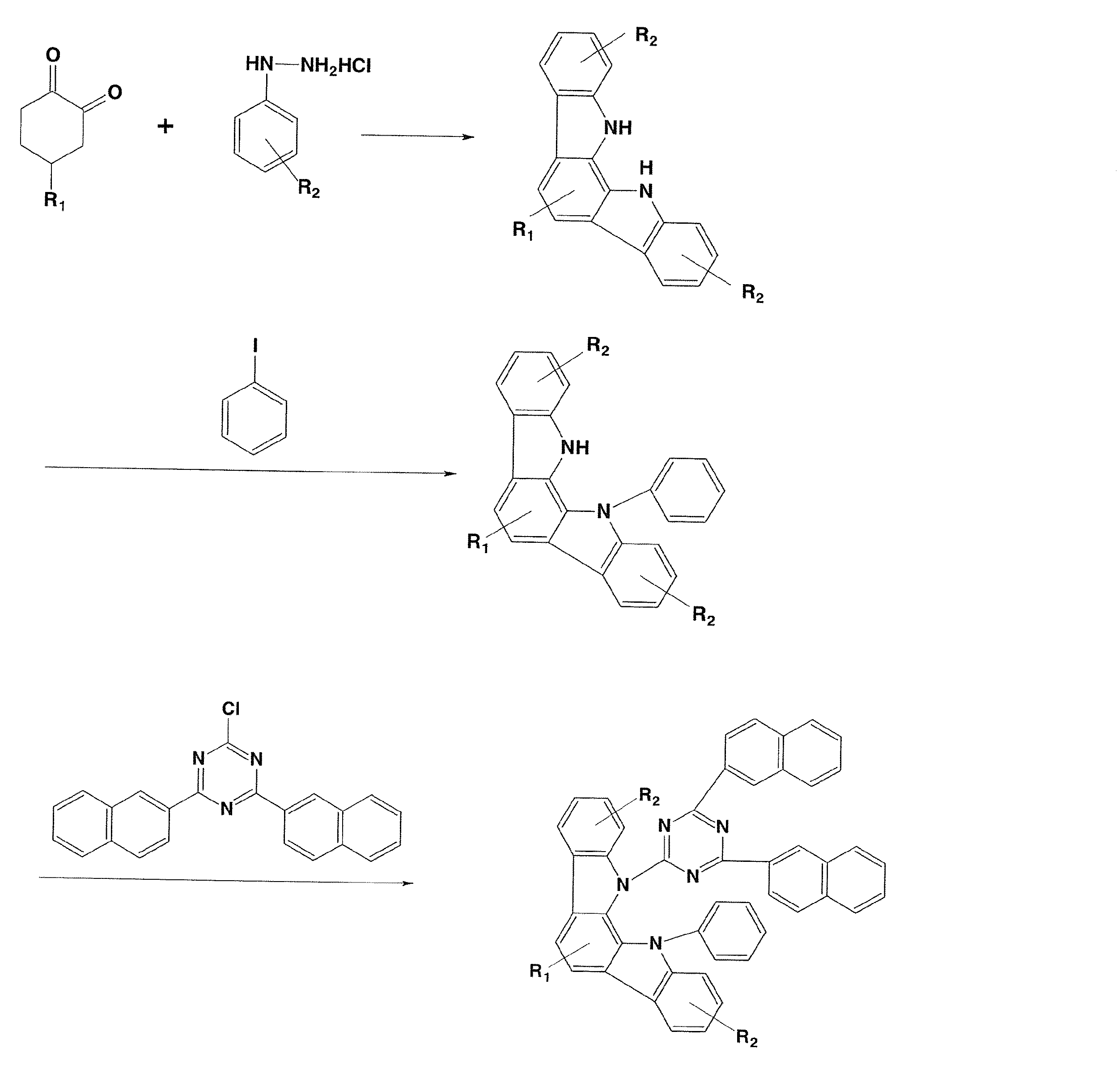
実施例1
(化合物21の合成)
脱気窒素置換した200ml三口フラスコに1,2-シクロヘキサンジオン33.3g(0.297mol)、フェニルヒドラジン塩酸塩86.0g(0.595mol)を加え、これにエタノール1000mlを加えて攪拌させた。その後、同フラスコ内に濃硫酸3.0g(0.03mol)を5分間かけ滴下した。その後65℃まで加熱し、4時間攪拌した。室温まで冷却した後、生じた紫茶色結晶を濾取した後、濾取した結晶をエタノール500mlで二回、リスラリー洗浄をおこなった。これを、減圧乾燥して紫茶色粉末80.0g(0.286mol、収率96.3%)を得た。Example 1
(Synthesis of Compound 21)
To a 200 ml three-necked flask purged with degassed nitrogen, 33.3 g (0.297 mol) of 1,2-cyclohexanedione and 86.0 g (0.595 mol) of phenylhydrazine hydrochloride were added, and 1000 ml of ethanol was added thereto and stirred. Thereafter, 3.0 g (0.03 mol) of concentrated sulfuric acid was dropped into the flask over 5 minutes. Thereafter, the mixture was heated to 65 ° C. and stirred for 4 hours. After cooling to room temperature, the resulting purple brown crystals were collected by filtration, and the crystals thus collected were washed twice with 500 ml of ethanol and reslurry washed. This was dried under reduced pressure to obtain 80.0 g (0.286 mol, yield 96.3%) of a purple brown powder.
次に、上記紫茶色粉末72.0g(0.258mol)に、これに酢酸720g、トリフルオロ酢酸72.0gを加えて攪拌させた。その後100℃まで加熱し、15時間攪拌した。室温まで冷却した後、生じた黄色結晶を濾取した後、濾取した結晶を酢酸200mlでリンス洗浄をおこなった後、ヘキサン200mlでリンス洗浄をおこなった。これを、減圧乾燥して白色粉末A 30.0g(0.117mol、収率45.3%)を得た。 Next, 720 g of acetic acid and 72.0 g of trifluoroacetic acid were added to 72.0 g (0.258 mol) of the purple brown powder and stirred. Thereafter, the mixture was heated to 100 ° C. and stirred for 15 hours. After cooling to room temperature, the resulting yellow crystals were collected by filtration, rinsed with 200 ml of acetic acid, and then rinsed with 200 ml of hexane. This was dried under reduced pressure to obtain 30.0 g (0.117 mol, yield 45.3%) of white powder A.
次に、脱気窒素置換した1000ml三口フラスコに上記で得た白色粉末A26.0g(0.101mol)、ヨードベンゼン122.7g(0.601mol)、よう化銅54.7g(0.287mol)、炭酸カリウム66.7g(0.482mol)、これにキノリン8 00mlを加えて攪拌させた。その後190℃まで加熱し、72時間攪拌した。一旦、室温まで冷却した後、水500ml、ジクロロメタン500mlを加え、攪拌を行った後、生じた黄色結晶を濾取した。濾液を2000ml分液ロートへ移し、有機層と水層に分画した。有機層を500mlの水で三回洗浄し、その後、得られた有機層を硫酸マグネシウムで脱水を行い、一旦、硫酸マグネシウムを濾別した後、溶媒を減圧留去した。その後、カラムクロマトグラフィーで精製して白色粉末B 13.7g(0.04mol、収率40.8%)を得た。 Next, a white powder A26.0 g (0.101 mol) obtained above, 122.7 g (0.601 mol) iodobenzene, 54.7 g (0.287 mol) copper iodide, 66.7 g potassium carbonate (into a 1000 ml three-necked flask purged with nitrogen) 0.482 mol), 800 ml of quinoline was added thereto and stirred. Thereafter, the mixture was heated to 190 ° C. and stirred for 72 hours. After cooling to room temperature, 500 ml of water and 500 ml of dichloromethane were added and stirred, and the resulting yellow crystals were collected by filtration. The filtrate was transferred to a 2000 ml separatory funnel and separated into an organic layer and an aqueous layer. The organic layer was washed three times with 500 ml of water, and then the obtained organic layer was dehydrated with magnesium sulfate. After magnesium sulfate was filtered off once, the solvent was distilled off under reduced pressure. Thereafter, the residue was purified by column chromatography to obtain 13.7 g (0.04 mol, yield 40.8%) of white powder B.
次に、脱気窒素置換した500ml三口フラスコに55%水素化ナトリウム2.16g(0.0495mol)、脱水N,N’-ジメチルホルムアミド70mlを加え、窒素気流中下で攪拌を行う。上記で得た白色粉末B 13.7g(0.04mol)に脱水N,N’-ジメチルホルムアミド70mlを加え、溶解させ、その後、同フラスコ内に15分間かけ滴下した。滴下終了後、1時間攪拌を継続した。その後、塩化シアヌル3.76g(0.02mol)に脱水N,N’-ジメチルホルムアミド70mlを加え、溶解させ、その後、同フラスコ内に15分間かけ滴下した。滴下終了後、2時間攪拌を継続した後、水350gを加え、析出した結晶を濾取した。濾取した結晶を水300gで二回リスラリーを行い、その後、メタノール300gにてリスラリーを行った。これを減圧乾燥した後、カラムクロマトグラフィーで精製して白色粉末C 10.9g(0.014mol、収率70.0%)を得た。 Next, 2.16 g (0.0495 mol) of 55% sodium hydride and 70 ml of dehydrated N, N′-dimethylformamide are added to a 500 ml three-necked flask purged with degassed nitrogen, and the mixture is stirred in a nitrogen stream. To 13.7 g (0.04 mol) of the white powder B obtained above, 70 ml of dehydrated N, N'-dimethylformamide was added and dissolved, and then dropped into the flask over 15 minutes. After completion of dropping, stirring was continued for 1 hour. Thereafter, 70 ml of dehydrated N, N′-dimethylformamide was added to 3.76 g (0.02 mol) of cyanuric chloride and dissolved, and then dropped into the flask over 15 minutes. After completion of the dropwise addition, stirring was continued for 2 hours, 350 g of water was added, and the precipitated crystals were collected by filtration. The crystals collected by filtration were reslurried twice with 300 g of water, and then reslurried with 300 g of methanol. This was dried under reduced pressure and purified by column chromatography to obtain 10.9 g (0.014 mol, yield 70.0%) of white powder C.
次に、300ml三口フラスコに上記で得た白色粉末C 10.0g(0.013mol)、2-ナフチルボロン酸2.8g(0.016mol)、テトラキス(トリフェニルホスフィン)パラジウム(0)1.5g(0.0013mol)エタノール50ml、トルエン100mlを加えて攪拌させた。その後、炭酸ナトリウム6.5gを水50mlに溶解させ、同フラスコ内に加え85℃まで加熱し、5時間攪拌した。一旦、室温まで冷却した後、水100ml、トルエン100mlを加え、攪拌を行った後、不溶物を濾別した。濾液を1000ml分液ロートへ移し、有機層と水層に分画した。有機層を100mlの水で三回洗浄し、その後、得られた有機層を硫酸マグネシウムで脱水を行い、一旦、硫酸マグネシウムを濾別した後、溶媒を減圧留去した。その後、カラムクロマトグラフィーで精製して黄色固体の例示化合物21を34.7g(0.04mol、収率40.8%)得た。
例示化合物21のEI−MS(M+1)は868、融点は398℃であった。Next, in a 300 ml three-necked flask, 10.0 g (0.013 mol) of white powder C obtained above, 2.8 g (0.016 mol) of 2-naphthylboronic acid, 1.5 g (0.0013 mol) ethanol of tetrakis (triphenylphosphine) palladium (0) 50 ml and 100 ml of toluene were added and stirred. Thereafter, 6.5 g of sodium carbonate was dissolved in 50 ml of water, added to the flask, heated to 85 ° C., and stirred for 5 hours. After cooling to room temperature, 100 ml of water and 100 ml of toluene were added and stirred, and then insoluble matter was filtered off. The filtrate was transferred to a 1000 ml separatory funnel and separated into an organic layer and an aqueous layer. The organic layer was washed three times with 100 ml of water, and then the obtained organic layer was dehydrated with magnesium sulfate. After magnesium sulfate was filtered off once, the solvent was distilled off under reduced pressure. Thereafter, the residue was purified by column chromatography to obtain 34.7 g (0.04 mol, yield 40.8%) of Exemplary Compound 21 as a yellow solid.
Illustrative compound 21 had an EI-MS (M + 1) of 868 and a melting point of 398 ° C.
実施例2
正孔注入層に銅フタロシアニン(CuPC)を用い、正孔輸送層にα-NPD及び電子輸送層にAlq3を用いた。膜厚150nmのITOからなる陽極が形成されたガラス基板上に、各薄膜を真空蒸着法にて、真空度5.0×10⁻⁴ Paで積層させた。まず、ITO上に正孔注入層としてCuPCを3.0Å/秒で25 nmの膜厚で成膜した。次いで、正孔注入層上に、正孔輸送層としてα-NPDを蒸着速度3.0Å/秒にて55nmの厚さに形成した。Example 2
Copper phthalocyanine (CuPC) was used for the hole injection layer, α-NPD for the hole transport layer, and Alq3 for the electron transport layer. Each thin film was laminated at a vacuum degree of 5.0 × 10 −4 Pa by a vacuum deposition method on a glass substrate on which an anode made of ITO having a thickness of 150 nm was formed. First, CuPC was deposited on ITO as a hole injection layer at a thickness of 25 nm at 3.0 mm / sec. Next, α-NPD was formed as a hole transport layer on the hole injection layer to a thickness of 55 nm at a deposition rate of 3.0 kg / sec.
次に、正孔輸送層上に、発光層として(例示化合物21)と(Btp)2Iracac(例示化合物41)とを異なる蒸着源から共蒸着し、47.5nmの厚さに形成した。この時、(Btp)2Iracacの濃度は8.0 %であった。
次に、電子輸送層としてAlq3を蒸着速度3.0Å/秒にて30nmの厚さに形成した。更に、電子輸送層上に、電子注入層としフッ化リチウム(LiF)を蒸着速度0.1Å/秒にて1nmの厚さに形成した。最後に、電子注入層上に、電極としてアルミニウム(Al)を蒸着速度10Å/秒にて200nmの厚さに形成し、有機EL素子を作成した。Next, (Exemplary Compound 21) and (Btp) 2Iracac (Exemplary Compound 41) were co-deposited from different vapor deposition sources on the hole transport layer as a light emitting layer to form a thickness of 47.5 nm. At this time, the concentration of (Btp) 2Iracac was 8.0%.
Next, Alq3 was formed as an electron transport layer to a thickness of 30 nm at a deposition rate of 3.0 liters / second. Further, on the electron transport layer, lithium fluoride (LiF) was formed as an electron injection layer to a thickness of 1 nm at a deposition rate of 0.1 kg / sec. Finally, on the electron injection layer, aluminum (Al) was formed as an electrode to a thickness of 200 nm at a vapor deposition rate of 10 Å / sec, thereby producing an organic EL device.
実施例3
(化合物4の合成)
窒素置換した200ml三口フラスコに実施例1で得られた白色粉末A10.0g(0.036mol)、炭酸カリウム12.9g(0.093mol)、銅粉5.7g(0.090mol)、テトラグライム50.0gを加え、窒素気流下で攪拌した。同フラスコ内に2-ブロモナフタレン9.87g(0.047mol)をテトラグライム10.0gに溶解させた溶液を10分間かけ滴下した。滴下終了後、195℃で1時間攪拌を継続した。その後、室温まで冷却し、不溶物を濾取した。濾液にメタノール30gおよび水150gを加え、2時間攪拌した。その後、析出物を濾取し、これを水100gで2回、更に、メタノール100gで1回リスラリー洗浄した。減圧乾燥後、カラムクロマトグラフィーで精製して白色粉末D 13.0g(0.034mol、収率94.7%)を得た。Example 3
(Synthesis of Compound 4)
To a 200 ml three-necked flask substituted with nitrogen, add 10.0 g (0.036 mol) of white powder A obtained in Example 1, 12.9 g (0.093 mol) of potassium carbonate, 5.7 g (0.090 mol) of copper powder, and 50.0 g of tetraglyme. Stirred under a stream of air. A solution prepared by dissolving 9.87 g (0.047 mol) of 2-bromonaphthalene in 10.0 g of tetraglyme was dropped into the flask over 10 minutes. After completion of the dropping, stirring was continued at 195 ° C. for 1 hour. Then, it cooled to room temperature and filtered the insoluble matter. 30 g of methanol and 150 g of water were added to the filtrate and stirred for 2 hours. Thereafter, the precipitate was collected by filtration and washed with reslurry twice with 100 g of water and once with 100 g of methanol. After drying under reduced pressure, the residue was purified by column chromatography to obtain 13.0 g (0.034 mol, yield 94.7%) of white powder D.
次に、窒素置換した200ml三口フラスコに、塩化シアヌル12.5g(0.068mol)、脱水THF 50gを加え、窒素気流下、氷浴により冷却し攪拌した。その後、32%臭化フェニルマグネシウムTHF溶液 105.6g(0.186mol)を2時間かけ滴下した。滴下中の温度は15℃以下を保った。滴下終了後、1.5時間攪拌を継続した後、同フラスコ内にトルエン80gを加えた。その後、氷浴にて冷却を行い、同フラスコ内に12%HClaq 76.5g(0.254mol)を15分かけ滴下した。滴下中の温度は30℃以下を保った。フラスコ内容物を500ml分液ロートへ移し、有機層と水層に分画した。有機層を100mlの水で三回洗浄し、その後、得られた有機層を硫酸マグネシウムで脱水し、一旦、硫酸マグネシウムを濾別した後、溶媒を減圧留去し21.1gのクルード品を得た。その後、メタノール110gを加え、1時間攪拌後、析出物を濾取し、減圧乾燥により白色粉末E 14.5g(6.5mmol、収率50.2%)を得た。 Next, 12.5 g (0.068 mol) of cyanuric chloride and 50 g of dehydrated THF were added to a nitrogen-substituted 200 ml three-necked flask, and the mixture was cooled and stirred in an ice bath under a nitrogen stream. Thereafter, 105.6 g (0.186 mol) of a 32% phenylmagnesium bromide THF solution was added dropwise over 2 hours. The temperature during the dropping was kept at 15 ° C. or lower. After completion of the dropwise addition, stirring was continued for 1.5 hours, and then 80 g of toluene was added to the flask. Thereafter, the mixture was cooled in an ice bath, and 76.5 g (0.254 mol) of 12% HClaq was dropped into the flask over 15 minutes. The temperature during the dropping was kept below 30 ° C. The contents of the flask were transferred to a 500 ml separatory funnel and fractionated into an organic layer and an aqueous layer. The organic layer was washed three times with 100 ml of water, and then the obtained organic layer was dehydrated with magnesium sulfate. After magnesium sulfate was filtered off, the solvent was distilled off under reduced pressure to obtain 21.1 g of a crude product. . Thereafter, 110 g of methanol was added and stirred for 1 hour. The precipitate was collected by filtration and dried under reduced pressure to obtain 14.5 g (6.5 mmol, yield 50.2%) of white powder E.
次に、窒素置換した200ml三口フラスコに、60.8%水素化ナトリウム1.31g(0.033mol)、脱水N,N’-ジメチルホルムアミド10mlを加え、窒素気流下で攪拌した。これに、上記で得た白色粉末D 10.0g(0.026mol)の脱水N,N’-ジメチルホルムアミド(30ml)溶液を、20分間かけ滴下した。滴下終了後、1時間攪拌を継続した。続いて、上記で得た白色粉末E 6.75g(0.025mol)の脱水N,N’-ジメチルホルムアミド(10ml)溶液を20分間かけ滴下した。滴下終了後、17時間攪拌を継続した。その後、水3.2g、メタノール40.0gを順に加え、析出した結晶を濾取した。これをメタノール50gにてリスラリー洗浄した後、減圧乾燥し、淡黄色結晶の例示化合物4を12.8g(0.021mol、収率80.0%)得た。
例示化合物4のAPCI−MSはm/Z 614[M+H]+、融点は317℃であった。Next, 1.31 g (0.033 mol) of 60.8% sodium hydride and 10 ml of dehydrated N, N′-dimethylformamide were added to a nitrogen-substituted 200 ml three-necked flask and stirred under a nitrogen stream. To this was added dropwise a dehydrated N, N′-dimethylformamide (30 ml) solution of 10.0 g (0.026 mol) of the white powder D obtained above over 20 minutes. After completion of dropping, stirring was continued for 1 hour. Subsequently, a solution of 6.75 g (0.025 mol) of the white powder E obtained above in dehydrated N, N′-dimethylformamide (10 ml) was added dropwise over 20 minutes. After completion of the dropwise addition, stirring was continued for 17 hours. Thereafter, 3.2 g of water and 40.0 g of methanol were sequentially added, and the precipitated crystals were collected by filtration. This was reslurried with 50 g of methanol and then dried under reduced pressure to obtain 12.8 g (0.021 mol, yield 80.0%) of Illustrative Compound 4 as pale yellow crystals.
APCI-MS of Exemplified Compound 4 was m / Z 614 [M + H] + , and melting point was 317 ° C.
実施例4
発光層のホスト材料として例示化合物21に代えて例示化合物4を用いた以外は実施例2と同様にして有機EL素子を作成した。Example 4
An organic EL device was produced in the same manner as in Example 2 except that Exemplified Compound 4 was used in place of Exemplified Compound 21 as the host material for the light emitting layer.
実施例5
(化合物5の合成例)
窒素置換した500ml三口フラスコに、マグネシウム3.65g(0.150mol)、脱水THF 10.0g、ヨウ素0.01gを加え、窒素気流下で攪拌した。60℃まで昇温した後、2-ブロモナフタレン32.1g(0.155mol)の脱水THF( 100.0ml)溶液を1時間かけ滴下した。その後、加熱還流下、2時間攪拌を続けた。室温まで冷却をした後、更に氷浴にて3℃まで冷却した。これに、塩化シアヌル9.21g(0.050mol)の脱水THF (50.0ml)溶解を、氷浴にて10℃以下に保ちながら30分間かけて滴下し、滴下終了後、更に室温で5時間攪拌した。その後、同フラスコを氷浴に浸し、15℃以下に保ちながら10%塩酸50.0gを30分間で滴下した。氷浴を外し、トルエン150.0mlを加え、500 ml分液ロートにて、有機層と水層に分画した。有機層を50mlの水で三回洗浄し、有機層を硫酸マグネシウムで脱水し、一旦、硫酸マグネシウムを濾別した後、溶媒を減圧留去することにより濃縮物33.6gを得た。得られた濃縮物を75.0gのTHFに溶解させ、攪拌しながらメタノール200.0gを徐々に加えた。析出した結晶を濾別しし、これをヘキサンにて再結晶し、7.6g(0.021mol、収率41.3%)の白色粉末Fを得た。Example 5
(Synthesis Example of Compound 5)
To a 500 ml three-necked flask purged with nitrogen, 3.65 g (0.150 mol) of magnesium, 10.0 g of dehydrated THF, and 0.01 g of iodine were added and stirred under a nitrogen stream. After the temperature was raised to 60 ° C., a solution of 32.1 g (0.155 mol) of 2-bromonaphthalene in dehydrated THF (100.0 ml) was added dropwise over 1 hour. Thereafter, stirring was continued for 2 hours while heating under reflux. After cooling to room temperature, it was further cooled to 3 ° C. in an ice bath. To this, 9.21 g (0.050 mol) of cyanuric chloride dissolved in dehydrated THF (50.0 ml) was added dropwise over 30 minutes while keeping it at 10 ° C. or lower in an ice bath. After completion of the addition, the mixture was further stirred at room temperature for 5 hours. Thereafter, the flask was immersed in an ice bath, and 50.0 g of 10% hydrochloric acid was added dropwise over 30 minutes while maintaining the temperature at 15 ° C. or lower. The ice bath was removed, 150.0 ml of toluene was added, and the mixture was separated into an organic layer and an aqueous layer with a 500 ml separatory funnel. The organic layer was washed three times with 50 ml of water, the organic layer was dehydrated with magnesium sulfate, and after magnesium sulfate was filtered off, the solvent was distilled off under reduced pressure to obtain 33.6 g of a concentrate. The obtained concentrate was dissolved in 75.0 g of THF, and 200.0 g of methanol was gradually added while stirring. The precipitated crystals were separated by filtration and recrystallized from hexane to obtain 7.6 g (0.021 mol, yield 41.3%) of white powder F.
次に、窒素置換した200ml三口フラスコに60.8%水素化ナトリウム0.98g(0.025mol)、脱水N,N’-ジメチルホルムアミド10mlを加え、窒素気流下で攪拌した。これに、実施例1で得た白色粉末B 6.45g(0.019mol)の脱水N,N’-ジメチルホルムアミド(20ml)溶液を20分間かけ滴下し、滴下終了後、更に1時間攪拌した。これを氷浴で冷却し、白色粉末F 7.0g(0.019mol)の脱水N,N’-ジメチルホルムアミド(10ml)溶液を、内温5℃以下に保ちながら10分間かけて滴下した。滴下終了後、室温で更に7時間攪拌した。その後、水4.0g、メタノール100.0gを加え、析出した結晶を濾取した。これをメタノール50gにてリスラリー洗浄した後、減圧乾燥し、黄色結晶の例示化合物5を 8.0g(0.012mol、収率62.1%)得た。
例示化合物5のAPCI−MSはm/Z 664[M+H]+、融点は355℃であった。Next, 0.98 g (0.025 mol) of 60.8% sodium hydride and 10 ml of dehydrated N, N′-dimethylformamide were added to a nitrogen-substituted 200 ml three-necked flask and stirred under a nitrogen stream. To this was added dropwise a dehydrated N, N′-dimethylformamide (20 ml) solution of 6.45 g (0.019 mol) of white powder B obtained in Example 1 over 20 minutes. After completion of the dropwise addition, the mixture was further stirred for 1 hour. This was cooled in an ice bath, and a solution of white powder F 7.0 g (0.019 mol) in dehydrated N, N′-dimethylformamide (10 ml) was added dropwise over 10 minutes while maintaining the internal temperature at 5 ° C. or lower. After completion of dropping, the mixture was further stirred at room temperature for 7 hours. Thereafter, 4.0 g of water and 100.0 g of methanol were added, and the precipitated crystals were collected by filtration. This was reslurried with 50 g of methanol and then dried under reduced pressure to obtain 8.0 g (0.012 mol, yield 62.1%) of
APCI-MS of
実施例6
発光層のホスト材料として例示化合物21に代えて例示化合物5を用いた以外は実施例2と同様にして有機EL素子を作成した。Example 6
An organic EL device was produced in the same manner as in Example 2 except that
実施例7(比較)
発光層のホスト材料として例示化合物21に代えてBAlqを用いた以外は実施例2と同様にして有機EL素子を作成した。Example 7 (comparison)
An organic EL device was produced in the same manner as in Example 2 except that BAlq was used instead of the exemplified compound 21 as the host material for the light emitting layer.
実施例で得られた有機EL素子各々の発光ピーク波長、最高発光効率、輝度半減寿命(初期輝度2,000cd/m2)を表1に示す。Table 1 shows the emission peak wavelength, maximum emission efficiency, and luminance half life (initial luminance 2,000 cd / m 2 ) of each organic EL device obtained in the examples.
本発明の有機EL素子は、低電圧において高輝度・高効率で発光させることが可能となる。したがって、本発明による有機EL素子はフラットパネル・ディスプレイ(例えばOAコンピュータ用や壁掛けテレビ)、車載表示素子、携帯電話表示や面発光体としての特徴を生かした光源(例えば、複写機の光源、液晶ディスプレイや計器類のバックライト光源)、表示板、標識灯への応用が考えられ、その技術的価値は大きいものである。 The organic EL device of the present invention can emit light with high luminance and high efficiency at a low voltage. Therefore, the organic EL device according to the present invention is a flat panel display (for example, for OA computers or wall-mounted televisions), an in-vehicle display device, a light source utilizing characteristics of a cellular phone display or a surface light emitter (for example, a light source of a copying machine, a liquid crystal). It can be applied to backlight sources for displays and instruments, display panels, and indicator lights, and its technical value is great.
Claims (7)
環aは、2つの隣接環と縮合する式(a1)で表される芳香環を示し、XはCHを示す。環bは、2つの隣接環と縮合する式(b1)で表される複素環を示し、
Ar1は、芳香族複素環基からなるm+n価の基を示し、
Lは独立に、置換若しくは未置換の芳香族炭化水素基又は芳香族複素環基を示し、少なくとも一つは縮環構造を有し、
Rは独立に、水素、アルキル基、アラルキル基、アルケニル基、アルキニル基、シアノ基、ジアルキルアミノ基、ジアリールアミノ基、ジアラルキルアミノ基、アミノ基、ニトロ基、アシル基、アルコキシカルボニル基、カルボキシル基、アルコキシル基、アルキルスルホニル基、ハロアルキル基、水酸基、アミド基、又は置換若しくは未置換の芳香族炭化水素基若しくは芳香族複素環基を示し、
mは1を示し、nは1又は2を示す。The compound for organic electroluminescent elements represented by the following general formula (I).
Ring a represents an aromatic ring represented by the formula (a1) fused with two adjacent rings, and X represents CH . Ring b represents a heterocycle represented by the formula (b1) fused with two adjacent rings,
Ar 1 represents an m + n-valent group consisting of an aromatic heterocyclic group,
L independently represents a substituted or unsubstituted aromatic hydrocarbon group or aromatic heterocyclic group, at least one of which has a condensed ring structure,
R is independently hydrogen, alkyl group, aralkyl group, alkenyl group, alkynyl group, cyano group, dialkylamino group, diarylamino group, diaralkylamino group, amino group, nitro group, acyl group, alkoxycarbonyl group, carboxyl group , An alkoxyl group, an alkylsulfonyl group, a haloalkyl group, a hydroxyl group, an amide group, or a substituted or unsubstituted aromatic hydrocarbon group or aromatic heterocyclic group,
m represents 1 and n represents 1 or 2.
環a、環b、L及びRは、一般式(I)の環a、環b、L及びRと同じ意味を有し、
Ar2は式(c1)で表される3価の基であり、Yは独立にCH又はNを示し、少なくとも一つはNである。2. The compound for organic electroluminescence device according to claim 1, represented by the following general formula (II):
Ring a, Ring b, L and R have the same meaning as Ring a, Ring b, L and R of general formula (I),
Ar 2 is a trivalent group represented by the formula (c1), Y independently represents CH or N, and at least one is N.
L、R及びAr2は、一般式(II)のL、R及びAr2と同じ意味を有する。3. The compound for organic electroluminescence device according to claim 2, represented by the following general formula (III) or (IV):
L, R and Ar 2 have L of formula (II), the same meaning as R and Ar 2.
Applications Claiming Priority (3)
| Application Number | Priority Date | Filing Date | Title |
|---|---|---|---|
| JP2007142274 | 2007-05-29 | ||
| JP2007142274 | 2007-05-29 | ||
| PCT/JP2008/059807 WO2008146839A1 (en) | 2007-05-29 | 2008-05-28 | Compound for organic electroluminescent device and organic electroluminescent device |
Publications (2)
| Publication Number | Publication Date |
|---|---|
| JPWO2008146839A1 JPWO2008146839A1 (en) | 2010-08-19 |
| JP4550160B2 true JP4550160B2 (en) | 2010-09-22 |
Family
ID=40075076
Family Applications (1)
| Application Number | Title | Priority Date | Filing Date |
|---|---|---|---|
| JP2009516335A Active JP4550160B2 (en) | 2007-05-29 | 2008-05-28 | Compound for organic electroluminescent device and organic electroluminescent device |
Country Status (7)
| Country | Link |
|---|---|
| US (1) | US8008657B2 (en) |
| EP (2) | EP2759545B1 (en) |
| JP (1) | JP4550160B2 (en) |
| KR (1) | KR101041642B1 (en) |
| CN (1) | CN101679438B (en) |
| TW (1) | TWI468489B (en) |
| WO (1) | WO2008146839A1 (en) |
Cited By (1)
| Publication number | Priority date | Publication date | Assignee | Title |
|---|---|---|---|---|
| US11871659B2 (en) | 2019-02-15 | 2024-01-09 | Samsung Sdi Co., Ltd. | Composition for optoelectronic device and organic optoelectronic device and display device |
Families Citing this family (56)
| Publication number | Priority date | Publication date | Assignee | Title |
|---|---|---|---|---|
| CN101679852B (en) * | 2007-05-30 | 2012-12-05 | 新日铁化学株式会社 | Compound for organic electroluminescent device and organic electroluminescent device |
| EP2284920B1 (en) * | 2008-05-08 | 2015-07-29 | Nippon Steel & Sumikin Chemical Co., Ltd. | Compound for organic electric field light-emitting element and organic electric field light-emitting element |
| WO2009148015A1 (en) * | 2008-06-05 | 2009-12-10 | 出光興産株式会社 | Halogen compound, polycyclic compound, and organic electroluminescence element comprising the polycyclic compound |
| US8049411B2 (en) | 2008-06-05 | 2011-11-01 | Idemitsu Kosan Co., Ltd. | Material for organic electroluminescence device and organic electroluminescence device using the same |
| DE102008064200A1 (en) * | 2008-12-22 | 2010-07-01 | Merck Patent Gmbh | Organic electroluminescent device |
| US8795852B2 (en) | 2009-02-27 | 2014-08-05 | Nippon Steel & Sumikin Chemical Co., Ltd. | Organic electroluminescent device with host materials having same or similar IP, EA and T1 values |
| US8759818B2 (en) | 2009-02-27 | 2014-06-24 | E I Du Pont De Nemours And Company | Deuterated compounds for electronic applications |
| KR101511072B1 (en) * | 2009-03-20 | 2015-04-10 | 롬엔드하스전자재료코리아유한회사 | Novel organic electroluminescent compounds and organic electroluminescent device using the same |
| JP5723764B2 (en) * | 2009-03-31 | 2015-05-27 | 新日鉄住金化学株式会社 | Organic electroluminescence device |
| TWI471405B (en) * | 2009-03-31 | 2015-02-01 | Nippon Steel & Sumikin Chem Co | A phosphorescent element material, and an organic electroluminescent device using the same |
| US8497495B2 (en) * | 2009-04-03 | 2013-07-30 | E I Du Pont De Nemours And Company | Electroactive materials |
| KR101174088B1 (en) * | 2009-06-25 | 2012-08-14 | 제일모직주식회사 | Compounds?for organic photoelectric?device and organic photoelectric?device containing the same |
| DE102009031021A1 (en) | 2009-06-30 | 2011-01-05 | Merck Patent Gmbh | Materials for organic electroluminescent devices |
| JP4564584B1 (en) * | 2009-08-31 | 2010-10-20 | 富士フイルム株式会社 | Organic electroluminescence device |
| JP5457907B2 (en) | 2009-08-31 | 2014-04-02 | ユー・ディー・シー アイルランド リミテッド | Organic electroluminescence device |
| JP5715142B2 (en) * | 2009-09-29 | 2015-05-07 | イー・アイ・デュポン・ドウ・ヌムール・アンド・カンパニーE.I.Du Pont De Nemours And Company | Deuterium compounds for luminescence applications |
| WO2011059463A1 (en) * | 2009-10-29 | 2011-05-19 | E. I. Du Pont De Nemours And Company | Deuterated compounds for electronic applications |
| DE102009052428A1 (en) | 2009-11-10 | 2011-05-12 | Merck Patent Gmbh | Connection for electronic devices |
| EP3176241A1 (en) * | 2009-12-07 | 2017-06-07 | Nippon Steel & Sumikin Chemical Co., Ltd. | Organic light-emitting material and organic light-emitting element |
| EP2517275B1 (en) | 2009-12-22 | 2018-11-07 | Merck Patent GmbH | Formulations comprising phase-separated functional materials |
| WO2011076314A1 (en) | 2009-12-22 | 2011-06-30 | Merck Patent Gmbh | Electroluminescent formulations |
| JP5897472B2 (en) | 2009-12-22 | 2016-03-30 | メルク パテント ゲーエムベーハー | Electroluminescent functional surfactant |
| US9260433B2 (en) | 2009-12-28 | 2016-02-16 | Nippon Steel & Sumikin Chemical Co., Ltd. | Organic electroluminescent device |
| DE102010009193B4 (en) | 2010-02-24 | 2022-05-19 | MERCK Patent Gesellschaft mit beschränkter Haftung | Composition containing fluorine-fluorine associates, processes for their production, their use and organic electronic devices containing them |
| KR20130020883A (en) | 2010-03-11 | 2013-03-04 | 메르크 파텐트 게엠베하 | Fibers in therapy and cosmetics |
| JP2013522816A (en) | 2010-03-11 | 2013-06-13 | メルク パテント ゲーエムベーハー | Light emitting fiber |
| JP5577122B2 (en) * | 2010-03-18 | 2014-08-20 | 新日鉄住金化学株式会社 | Organic electroluminescence device |
| WO2011147522A1 (en) | 2010-05-27 | 2011-12-01 | Merck Patent Gmbh | Compositions comprising quantum dots |
| US20130226268A1 (en) | 2010-07-26 | 2013-08-29 | Merck Patent Gmbh | Nanocrystals in devices |
| WO2012013272A1 (en) | 2010-07-26 | 2012-02-02 | Merck Patent Gmbh | Quantum dots and hosts |
| KR20120030941A (en) * | 2010-09-20 | 2012-03-29 | 롬엔드하스전자재료코리아유한회사 | Novel organic electroluminescent compounds and organic electroluminescent device using the same |
| EP2655547A1 (en) | 2010-12-20 | 2013-10-30 | E.I. Du Pont De Nemours And Company | Compositions for electronic applications |
| JP5756288B2 (en) * | 2010-12-28 | 2015-07-29 | 出光興産株式会社 | Fused polycyclic compound, material for organic electroluminescence device, and organic electroluminescence device using the same |
| US9492681B2 (en) | 2011-02-14 | 2016-11-15 | Merck Patent Gmbh | Device and method for treatment of cells and cell tissue |
| US9537107B2 (en) | 2011-03-14 | 2017-01-03 | Toray Industries, Inc. | Light emitting device material and light emitting device |
| WO2012126566A1 (en) | 2011-03-24 | 2012-09-27 | Merck Patent Gmbh | Organic ionic functional materials |
| WO2012149992A1 (en) | 2011-05-04 | 2012-11-08 | Merck Patent Gmbh | Device for preserving fresh goods |
| WO2012152366A1 (en) | 2011-05-12 | 2012-11-15 | Merck Patent Gmbh | Organic ionic compounds, compositions and electronic devices |
| WO2012153725A1 (en) | 2011-05-12 | 2012-11-15 | 東レ株式会社 | Light-emitting element material and light-emitting element |
| KR20140094520A (en) | 2011-10-26 | 2014-07-30 | 이데미쓰 고산 가부시키가이샤 | Organic electroluminescence element, and material for organic electroluminescence element |
| US20160276599A1 (en) * | 2012-01-18 | 2016-09-22 | Duk San Neolux Co., Ltd. | Compound for organic electric element, organic electric element comprising the same and electronic device thereof |
| KR20140123555A (en) | 2012-01-30 | 2014-10-22 | 메르크 파텐트 게엠베하 | Nanocrystals on fibers |
| EP2827397B1 (en) | 2012-03-12 | 2019-04-03 | NIPPON STEEL Chemical & Material Co., Ltd. | Organic electroluminescent element |
| EP2879196B1 (en) | 2012-07-25 | 2019-06-19 | Toray Industries, Inc. | Light emitting element material and light emitting element |
| TWI599570B (en) | 2012-09-28 | 2017-09-21 | 新日鐵住金化學股份有限公司 | Compounds for organic electroluminescent devices and organic electroluminescent devices |
| CN106608878A (en) * | 2015-10-26 | 2017-05-03 | 昱镭光电科技股份有限公司 | Organic material for organic electroluminescence device |
| KR102516810B1 (en) * | 2019-09-30 | 2023-03-30 | 삼성에스디아이 주식회사 | Compound for organic optoelectronic device, composition for organic optoelectronic device, organic optoelectronic device and display device |
| WO2021213917A1 (en) | 2020-04-21 | 2021-10-28 | Merck Patent Gmbh | Emulsions comprising organic functional materials |
| WO2022124366A1 (en) | 2020-12-11 | 2022-06-16 | 日鉄ケミカル&マテリアル株式会社 | Organic electroluminescent element |
| JPWO2022124365A1 (en) | 2020-12-11 | 2022-06-16 | ||
| KR20230119634A (en) | 2020-12-11 | 2023-08-16 | 닛테츠 케미컬 앤드 머티리얼 가부시키가이샤 | Materials for organic electroluminescent devices and organic electroluminescent devices |
| CN112876412B (en) * | 2021-01-21 | 2022-05-24 | 温州大学 | Doped luminescent material and preparation method and application thereof |
| CN114105997B (en) * | 2021-01-28 | 2023-05-19 | 陕西莱特光电材料股份有限公司 | Nitrogen-containing compound, and electronic element and electronic device comprising same |
| WO2023012084A1 (en) | 2021-08-02 | 2023-02-09 | Merck Patent Gmbh | A printing method by combining inks |
| CN114456172B (en) * | 2021-10-28 | 2023-06-23 | 陕西莱特迈思光电材料有限公司 | Nitrogen-containing compound, and electronic component and electronic device comprising same |
| WO2023237458A1 (en) | 2022-06-07 | 2023-12-14 | Merck Patent Gmbh | Method of printing a functional layer of an electronic device by combining inks |
Citations (5)
| Publication number | Priority date | Publication date | Assignee | Title |
|---|---|---|---|---|
| JPH11144866A (en) * | 1997-11-05 | 1999-05-28 | Toray Ind Inc | Electroluminescent element |
| JPH11162650A (en) * | 1997-10-02 | 1999-06-18 | Xerox Corp | Electroluminescent device |
| JPH11176578A (en) * | 1997-10-02 | 1999-07-02 | Xerox Corp | Electroluminescent device using indolo carbazole |
| JP2003515897A (en) * | 1999-12-01 | 2003-05-07 | ザ、トラスティーズ オブ プリンストン ユニバーシティ | Complexes of Formula L2MX as phosphorescent dopants for organic LEDs |
| JP2004204234A (en) * | 2002-12-24 | 2004-07-22 | Samsung Sdi Co Ltd | Blue light-emitting polymer and organic el element using the same |
Family Cites Families (12)
| Publication number | Priority date | Publication date | Assignee | Title |
|---|---|---|---|---|
| JP2001313178A (en) | 2000-04-28 | 2001-11-09 | Pioneer Electronic Corp | Organic electroluminescent element |
| JP2002305083A (en) | 2001-04-04 | 2002-10-18 | Mitsubishi Chemicals Corp | Organic electroluminescent element |
| JP2002352957A (en) | 2001-05-23 | 2002-12-06 | Honda Motor Co Ltd | Organic electoluminescence element |
| JP4011325B2 (en) | 2001-10-31 | 2007-11-21 | パイオニア株式会社 | Organic electroluminescence device |
| US7402681B2 (en) | 2004-12-14 | 2008-07-22 | Xerox Corporation | Compound with indolocarbazole moieties and devices containing such compound |
| US20060124921A1 (en) | 2004-12-14 | 2006-06-15 | Xerox Corporation | Compound with indolocarbazole moieties and devices containing such compound |
| JP4593631B2 (en) | 2005-12-01 | 2010-12-08 | 新日鐵化学株式会社 | Compound for organic electroluminescence device and organic electroluminescence device |
| CN101371377A (en) | 2005-12-01 | 2009-02-18 | 新日铁化学株式会社 | Organic electroluminescent device |
| CN101511834B (en) * | 2006-11-09 | 2013-03-27 | 新日铁化学株式会社 | Compound for organic electroluminescent device and organic electroluminescent device |
| CN101679852B (en) * | 2007-05-30 | 2012-12-05 | 新日铁化学株式会社 | Compound for organic electroluminescent device and organic electroluminescent device |
| TWI472074B (en) * | 2008-03-17 | 2015-02-01 | Nippon Steel & Sumikin Chem Co | Organic electroluminescent elements |
| EP2284920B1 (en) * | 2008-05-08 | 2015-07-29 | Nippon Steel & Sumikin Chemical Co., Ltd. | Compound for organic electric field light-emitting element and organic electric field light-emitting element |
-
2008
- 2008-05-27 TW TW97119549A patent/TWI468489B/en not_active IP Right Cessation
- 2008-05-28 US US12/600,773 patent/US8008657B2/en active Active
- 2008-05-28 EP EP14161321.6A patent/EP2759545B1/en active Active
- 2008-05-28 KR KR1020097025724A patent/KR101041642B1/en active IP Right Grant
- 2008-05-28 WO PCT/JP2008/059807 patent/WO2008146839A1/en active Application Filing
- 2008-05-28 JP JP2009516335A patent/JP4550160B2/en active Active
- 2008-05-28 EP EP08776922.0A patent/EP2166011B1/en active Active
- 2008-05-28 CN CN200880015477XA patent/CN101679438B/en active Active
Patent Citations (5)
| Publication number | Priority date | Publication date | Assignee | Title |
|---|---|---|---|---|
| JPH11162650A (en) * | 1997-10-02 | 1999-06-18 | Xerox Corp | Electroluminescent device |
| JPH11176578A (en) * | 1997-10-02 | 1999-07-02 | Xerox Corp | Electroluminescent device using indolo carbazole |
| JPH11144866A (en) * | 1997-11-05 | 1999-05-28 | Toray Ind Inc | Electroluminescent element |
| JP2003515897A (en) * | 1999-12-01 | 2003-05-07 | ザ、トラスティーズ オブ プリンストン ユニバーシティ | Complexes of Formula L2MX as phosphorescent dopants for organic LEDs |
| JP2004204234A (en) * | 2002-12-24 | 2004-07-22 | Samsung Sdi Co Ltd | Blue light-emitting polymer and organic el element using the same |
Cited By (1)
| Publication number | Priority date | Publication date | Assignee | Title |
|---|---|---|---|---|
| US11871659B2 (en) | 2019-02-15 | 2024-01-09 | Samsung Sdi Co., Ltd. | Composition for optoelectronic device and organic optoelectronic device and display device |
Also Published As
| Publication number | Publication date |
|---|---|
| CN101679438A (en) | 2010-03-24 |
| TWI468489B (en) | 2015-01-11 |
| EP2166011A1 (en) | 2010-03-24 |
| CN101679438B (en) | 2012-10-10 |
| WO2008146839A1 (en) | 2008-12-04 |
| KR101041642B1 (en) | 2011-06-14 |
| US8008657B2 (en) | 2011-08-30 |
| TW200914577A (en) | 2009-04-01 |
| JPWO2008146839A1 (en) | 2010-08-19 |
| EP2759545A1 (en) | 2014-07-30 |
| EP2166011B1 (en) | 2016-03-30 |
| EP2166011A4 (en) | 2011-08-17 |
| EP2759545B1 (en) | 2018-07-04 |
| US20100148161A1 (en) | 2010-06-17 |
| KR20100017737A (en) | 2010-02-16 |
Similar Documents
| Publication | Publication Date | Title |
|---|---|---|
| JP4550160B2 (en) | Compound for organic electroluminescent device and organic electroluminescent device | |
| JP4519946B2 (en) | Compound for organic electroluminescent device and organic electroluminescent device | |
| JP4593631B2 (en) | Compound for organic electroluminescence device and organic electroluminescence device | |
| JP4388590B2 (en) | Compound for organic electroluminescence device and organic electroluminescence device | |
| JP4819181B2 (en) | Compound for organic electroluminescence device and organic electroluminescence device | |
| JP5027947B2 (en) | Phosphorescent light emitting device material and organic electroluminescent device using the same | |
| JP4545741B2 (en) | Organic electroluminescence device | |
| JP4870245B2 (en) | Phosphorescent light emitting device material and organic electroluminescent device using the same | |
| JP4823730B2 (en) | Luminescent layer compound and organic electroluminescent device | |
| JP5009922B2 (en) | Organic electroluminescent element material and organic electroluminescent element | |
| WO2009119163A1 (en) | Compound for organic electroluminescent device and organic electroluminescent device using the same | |
| JP4864708B2 (en) | Organic electroluminescence device |
Legal Events
| Date | Code | Title | Description |
|---|---|---|---|
| TRDD | Decision of grant or rejection written | ||
| A01 | Written decision to grant a patent or to grant a registration (utility model) |
Free format text: JAPANESE INTERMEDIATE CODE: A01 Effective date: 20100706 |
|
| A01 | Written decision to grant a patent or to grant a registration (utility model) |
Free format text: JAPANESE INTERMEDIATE CODE: A01 |
|
| A61 | First payment of annual fees (during grant procedure) |
Free format text: JAPANESE INTERMEDIATE CODE: A61 Effective date: 20100707 |
|
| R150 | Certificate of patent or registration of utility model |
Ref document number: 4550160 Country of ref document: JP Free format text: JAPANESE INTERMEDIATE CODE: R150 Free format text: JAPANESE INTERMEDIATE CODE: R150 |
|
| FPAY | Renewal fee payment (event date is renewal date of database) |
Free format text: PAYMENT UNTIL: 20130716 Year of fee payment: 3 |
|
| FPAY | Renewal fee payment (event date is renewal date of database) |
Free format text: PAYMENT UNTIL: 20130716 Year of fee payment: 3 |
|
| S533 | Written request for registration of change of name |
Free format text: JAPANESE INTERMEDIATE CODE: R313533 |
|
| FPAY | Renewal fee payment (event date is renewal date of database) |
Free format text: PAYMENT UNTIL: 20130716 Year of fee payment: 3 |
|
| R350 | Written notification of registration of transfer |
Free format text: JAPANESE INTERMEDIATE CODE: R350 |
|
| FPAY | Renewal fee payment (event date is renewal date of database) |
Free format text: PAYMENT UNTIL: 20130716 Year of fee payment: 3 |
|
| FPAY | Renewal fee payment (event date is renewal date of database) |
Free format text: PAYMENT UNTIL: 20160716 Year of fee payment: 6 |
|
| S533 | Written request for registration of change of name |
Free format text: JAPANESE INTERMEDIATE CODE: R313533 |
|
| R350 | Written notification of registration of transfer |
Free format text: JAPANESE INTERMEDIATE CODE: R350 |
|
| S531 | Written request for registration of change of domicile |
Free format text: JAPANESE INTERMEDIATE CODE: R313531 |
|
| R350 | Written notification of registration of transfer |
Free format text: JAPANESE INTERMEDIATE CODE: R350 |
|
| R250 | Receipt of annual fees |
Free format text: JAPANESE INTERMEDIATE CODE: R250 |
|
| R250 | Receipt of annual fees |
Free format text: JAPANESE INTERMEDIATE CODE: R250 |