JP4546256B2 - How to safely change the data recorded on the memory card - Google Patents
How to safely change the data recorded on the memory card Download PDFInfo
- Publication number
- JP4546256B2 JP4546256B2 JP2004559826A JP2004559826A JP4546256B2 JP 4546256 B2 JP4546256 B2 JP 4546256B2 JP 2004559826 A JP2004559826 A JP 2004559826A JP 2004559826 A JP2004559826 A JP 2004559826A JP 4546256 B2 JP4546256 B2 JP 4546256B2
- Authority
- JP
- Japan
- Prior art keywords
- value
- data value
- memory location
- counter
- card
- Prior art date
- Legal status (The legal status is an assumption and is not a legal conclusion. Google has not performed a legal analysis and makes no representation as to the accuracy of the status listed.)
- Expired - Fee Related
Links
Images


Classifications
-
- G—PHYSICS
- G06—COMPUTING; CALCULATING OR COUNTING
- G06K—GRAPHICAL DATA READING; PRESENTATION OF DATA; RECORD CARRIERS; HANDLING RECORD CARRIERS
- G06K17/00—Methods or arrangements for effecting co-operative working between equipments covered by two or more of main groups G06K1/00 - G06K15/00, e.g. automatic card files incorporating conveying and reading operations
-
- G—PHYSICS
- G07—CHECKING-DEVICES
- G07F—COIN-FREED OR LIKE APPARATUS
- G07F7/00—Mechanisms actuated by objects other than coins to free or to actuate vending, hiring, coin or paper currency dispensing or refunding apparatus
- G07F7/08—Mechanisms actuated by objects other than coins to free or to actuate vending, hiring, coin or paper currency dispensing or refunding apparatus by coded identity card or credit card or other personal identification means
- G07F7/10—Mechanisms actuated by objects other than coins to free or to actuate vending, hiring, coin or paper currency dispensing or refunding apparatus by coded identity card or credit card or other personal identification means together with a coded signal, e.g. in the form of personal identification information, like personal identification number [PIN] or biometric data
- G07F7/1008—Active credit-cards provided with means to personalise their use, e.g. with PIN-introduction/comparison system
-
- G—PHYSICS
- G06—COMPUTING; CALCULATING OR COUNTING
- G06K—GRAPHICAL DATA READING; PRESENTATION OF DATA; RECORD CARRIERS; HANDLING RECORD CARRIERS
- G06K19/00—Record carriers for use with machines and with at least a part designed to carry digital markings
- G06K19/06—Record carriers for use with machines and with at least a part designed to carry digital markings characterised by the kind of the digital marking, e.g. shape, nature, code
- G06K19/067—Record carriers with conductive marks, printed circuits or semiconductor circuit elements, e.g. credit or identity cards also with resonating or responding marks without active components
- G06K19/07—Record carriers with conductive marks, printed circuits or semiconductor circuit elements, e.g. credit or identity cards also with resonating or responding marks without active components with integrated circuit chips
-
- G—PHYSICS
- G06—COMPUTING; CALCULATING OR COUNTING
- G06Q—INFORMATION AND COMMUNICATION TECHNOLOGY [ICT] SPECIALLY ADAPTED FOR ADMINISTRATIVE, COMMERCIAL, FINANCIAL, MANAGERIAL OR SUPERVISORY PURPOSES; SYSTEMS OR METHODS SPECIALLY ADAPTED FOR ADMINISTRATIVE, COMMERCIAL, FINANCIAL, MANAGERIAL OR SUPERVISORY PURPOSES, NOT OTHERWISE PROVIDED FOR
- G06Q20/00—Payment architectures, schemes or protocols
- G06Q20/30—Payment architectures, schemes or protocols characterised by the use of specific devices or networks
- G06Q20/34—Payment architectures, schemes or protocols characterised by the use of specific devices or networks using cards, e.g. integrated circuit [IC] cards or magnetic cards
- G06Q20/341—Active cards, i.e. cards including their own processing means, e.g. including an IC or chip
-
- G—PHYSICS
- G07—CHECKING-DEVICES
- G07F—COIN-FREED OR LIKE APPARATUS
- G07F7/00—Mechanisms actuated by objects other than coins to free or to actuate vending, hiring, coin or paper currency dispensing or refunding apparatus
- G07F7/08—Mechanisms actuated by objects other than coins to free or to actuate vending, hiring, coin or paper currency dispensing or refunding apparatus by coded identity card or credit card or other personal identification means
- G07F7/0806—Details of the card
- G07F7/0813—Specific details related to card security
- G07F7/082—Features insuring the integrity of the data on or in the card
-
- G—PHYSICS
- G07—CHECKING-DEVICES
- G07F—COIN-FREED OR LIKE APPARATUS
- G07F7/00—Mechanisms actuated by objects other than coins to free or to actuate vending, hiring, coin or paper currency dispensing or refunding apparatus
- G07F7/08—Mechanisms actuated by objects other than coins to free or to actuate vending, hiring, coin or paper currency dispensing or refunding apparatus by coded identity card or credit card or other personal identification means
- G07F7/0806—Details of the card
- G07F7/0833—Card having specific functional components
Landscapes
- Engineering & Computer Science (AREA)
- Physics & Mathematics (AREA)
- General Physics & Mathematics (AREA)
- Computer Security & Cryptography (AREA)
- Theoretical Computer Science (AREA)
- Business, Economics & Management (AREA)
- Microelectronics & Electronic Packaging (AREA)
- Strategic Management (AREA)
- Accounting & Taxation (AREA)
- General Business, Economics & Management (AREA)
- Computer Networks & Wireless Communication (AREA)
- Computer Hardware Design (AREA)
- Techniques For Improving Reliability Of Storages (AREA)
- Credit Cards Or The Like (AREA)
- Storage Device Security (AREA)
- Control Of Vending Devices And Auxiliary Devices For Vending Devices (AREA)
- Chair Legs, Seat Parts, And Backrests (AREA)
- Financial Or Insurance-Related Operations Such As Payment And Settlement (AREA)
- Information Retrieval, Db Structures And Fs Structures Therefor (AREA)
Abstract
Description
本発明は、カードリーダを用いた処理が実行されるとき、スマートカードに記録されているデータ記録の一部を変更するためのシステムに関し、さらに詳細には、スマートカードに記録されているデータを、リーダを用いた処理の間に変更するための安全な方法に関する。 The present invention relates to a system for changing a part of data recording recorded on a smart card when processing using a card reader is executed, and more particularly, to data recorded on a smart card. Relates to a secure method for changing during processing with a reader.
チップカードとも呼ばれるスマートカードは、カード所有者のデータキャリアとして益々その使用は増加している。これらのカードには、カードに搭載されたアンテナと、関連するリーダとの間の情報交換を非接触電磁結合により行う非接触カードが含まれる。これは、アクセス制限領域へのアクセスカード又は電子財布として開発されてきた。 Smart cards, also called chip cards, are increasingly used as cardholder data carriers. These cards include contactless cards that perform information exchange between the antenna mounted on the card and the associated reader by contactless electromagnetic coupling. This has been developed as an access card or electronic wallet to an access restricted area.
一般的に、スマートカードは不揮発性、消去および書換可能なEEPROM又はフラッシュEPROM型メモリを使用するので、メモリのスイッチが切れているときでもデータはメモリに書込まれたままである。これらはさらに、1つ又はいくつかのメモリ位置を消去して新しいデータを書込むことによりデータ記録を更新することが出来る。 In general, smart cards use non-volatile, erasable and rewritable EEPROM or flash EPROM type memory, so that data remains written to memory even when the memory is switched off. They can also update the data record by erasing one or several memory locations and writing new data.
処理の間に、一般的にはカードの「突然の取出し」、即ち処理動作が完了する前の取出し、による偶発的停電によりメモリが壊れ、それにより新しいデータが記録されずにデータを喪失することがある。このリスクが特に大きいのは、カードが正しく作動できる空間的限度を認知することの出来ない非接触カードを用いるときである。 During processing, the memory is corrupted due to an accidental power failure, typically due to “sudden removal” of the card, ie removal before the processing operation is completed, thereby losing data without new data being recorded. There is. This risk is particularly great when using contactless cards that cannot recognize the spatial limits at which the card can operate correctly.
不揮発性EEPROM型メモリの場合には、別のリスクがある。この場合、書込み動作が正常に終了する前に中断されてもデータは書込まれ、書込み動作の直後には正しく読取ることが出来るが、後の時点でこの読取りを繰返しても、これが正しく実行される保証はない。途中で中断された書込み動作の結果、メモリセル内の情報の保持が不十分だからである。 In the case of non-volatile EEPROM type memory, there is another risk. In this case, data is written even if it is interrupted before the writing operation is normally completed and can be read correctly immediately after the writing operation. However, even if this reading is repeated at a later time, this is executed correctly. There is no guarantee. This is because the information in the memory cell is not sufficiently retained as a result of the write operation interrupted halfway.
したがって、データの完全性を確保にするには、データが変更済み状態か、又は変更前の状態の何れかにあり、決して「突然の取出し」による未確定の中間状態にはならないことを確保することにより、このようなリスクに対してカードを保護することが望ましい。 Therefore, to ensure the integrity of the data, ensure that the data is either in the modified state or the state before the modification and never enters an indeterminate intermediate state due to "sudden retrieval". Therefore, it is desirable to protect the card against such risks.
処理の安全性の理由から、万一処理中に停電を生じ、処理を最初からやり直すことが出来ない場合は、重要データ(電子財布の預金残高など)の修復不能な喪失の危険を覚悟の上で、処理全体を再実行する必要がある。 If a power failure occurs during the process and the process cannot be restarted from the beginning for the reason of process safety, prepare for the risk of irreparable loss of important data (such as the deposit in the electronic wallet) Therefore, it is necessary to re-execute the entire process.
上述の問題に対応して、データ変更を実行する前にデータ記録をバッファメモリに記憶することが考案されてきた。変更すべき記録に対する変更が全て完了すると、古い記録はバッファメモリから消去される。 In response to the above problems, it has been devised to store data records in a buffer memory before performing data changes. When all changes to the record to be changed are completed, the old record is erased from the buffer memory.
残念なことに、この方法は、各記録毎に、バッファ領域への退避動作、変更すべき記録の消去動作、書換動作及びバッファ領域内の古い記録の消去動作と、全部で4つの動作を必要とする。したがってこの作業には、時間がかかる欠点があり、非接触カードにとっては重大な欠点である。 Unfortunately, this method requires a total of four operations for each recording: save operation to the buffer area, erase operation for the record to be changed, rewrite operation, and erase operation for the old record in the buffer area. And This operation therefore has the disadvantage of taking time and is a serious disadvantage for contactless cards.
さらに、前のデータを消去する前にメモリ内の別の位置に退避させるには、変更作業が正しく実行されたか否かをフラグ値に従って示すための「フラグ」の存在を必要とする。このフラグは、変更が正しく行われたか否かに従ってゼロ又は1の値を取る単一ビットにすることが出来る。データと同一位置にチェックビットを記録する明白な理由が考えられない限り、唯一の解決策は、このフラグ(単一又は複数のチェックビット)を、この目的に予約されたメモリ位置に記録することであり、したがって単一ビット又は数ビットで十分であれば、このためのメモリは全体で16ビット又は32ビットのブロックである。 Furthermore, in order to save the previous data to another position in the memory before erasing the previous data, it is necessary to have a “flag” for indicating whether or not the change operation is correctly executed according to the flag value. This flag can be a single bit that takes a value of zero or one depending on whether the change was made correctly. Unless there is an obvious reason to record the check bit in the same location as the data, the only solution is to record this flag (single or multiple check bits) in a memory location reserved for this purpose. Thus, if a single bit or a few bits are sufficient, the memory for this is a 16 or 32 bit block as a whole.
メモリ内の位置を浪費しないことが必須となる低容量のメモリのみが必要とされ、また処理毎に変更されるデータ値が時間の単調関数である特定の用途にスマートカードを使用する場合、上述の欠点はさらに重大である。このような用途において、メモリデータ記録は、写真複写機などのように時間と共に増加する増加カウンタか又は、記録の値が乗車毎に1単位ずつ減少する公共交通機関用カード若しくは記録の値が減少するだけの電子財布の場合の減少カウンタである。 When using smart cards for specific applications where only low-capacity memory is required that does not waste the location in memory, and the data value that changes from one process to another is a monotonic function of time, The disadvantages are even more serious. In such applications, the memory data record is an increase counter that increases with time, such as a photocopier, or a public transport card or record value that the record value decreases by one unit for each ride. It is a decrementing counter in the case of an electronic wallet.
したがって本発明の目的は、スマートカードの中のデータをカードの処理中に変更するための方法であって、処理中にカードが制限を受けるアクセス時間に対応する最少時間で実行できる方法を実現することにある。 Accordingly, an object of the present invention is to provide a method for changing data in a smart card during processing of the card, which can be executed in a minimum time corresponding to the access time that the card is restricted during processing. There is.
本発明の別の目的は、非接触型のスマートカードの中のデータを変更するための方法であって、メモリ位置にチェックビット(フラグ)を予約する必要のない方法を実現することにある。 Another object of the present invention is to implement a method for changing data in a contactless smart card that does not require reserving check bits (flags) at memory locations.
本発明の対象はしたがって、スマートカードなどや、カードがリーダに対し所定の位置関係にあるときカードを読取り可能なリーダと、を含むカード処理システムであって、そのカードは、カードによる処理に関するデータ値を記録するための少なくとも1つの位置を含む不揮発性、消去および書換可能なメモリを含み、各処理はデータ値の変更を生じ、データ値は時間に関し単調関数であるカード処理システムにおけるデータ変更方法である。データ値の書込み動作が、各処理毎に、メモリ内でカウンタを形成する所定の2つの位置のうちの第1位置に新しいデータ値の書込みを実行し、その書込み動作は、第2位置に記録される古いデータ値の消去を実行するので、正しく書込み動作が実行されると、第1位置に新しいデータ値を含み、第2位置に値ゼロを含む。 The subject of the present invention is therefore a card processing system comprising a smart card or the like and a reader capable of reading the card when the card is in a predetermined positional relationship with the reader, the card being data relating to processing by the card Method for changing data in a card processing system comprising a non-volatile, erasable and rewritable memory including at least one location for recording a value, each process resulting in a change in the data value, the data value being a monotonic function with respect to time It is. A data value write operation writes a new data value to the first of two predetermined positions forming a counter in the memory for each process, and the write operation is recorded at the second position. The old data value is erased, so that if the write operation is performed correctly, the first location contains the new data value and the second location contains the value zero.
本発明の対象及び特徴は、図面を参照して以下の記述を読むことにより、一層明確になる。 The objects and features of the invention will become more apparent upon reading the following description with reference to the drawings.
少量のメモリを必要とする用途に使用される布線論理メモリを有する型のチップカードでは、メモリ位置が限られている。このように、図1に示すようなチップカードのメモリはEPROM型メモリであって、16ビットの32ワードの容量を有する。以下に記述する本発明により、メモリ内でワード全部の予約を必要とするチェック領域を省くことが出来る。そのためには、2層カウンタを形成する2つのメモリ位置(A層、B層)が、リーダとスマートカードとの間で実行される各処理における新しいデータ値の記録に対して予約される。 In chip cards of the type having wired logic memory used for applications requiring a small amount of memory, the memory location is limited. Thus, the memory of the chip card as shown in FIG. 1 is an EPROM type memory and has a capacity of 32 words of 16 bits. According to the present invention described below, it is possible to omit a check area that requires reservation of all words in the memory. To do so, two memory locations (layer A, layer B) forming a two-layer counter are reserved for recording new data values in each process performed between the reader and the smart card.
本発明の原理は、それぞれの処理において変更されるデータ値が時間の単調関数である全ての用途において有効に利用される。アクセス制限領域へのアクセス、又は電子財布など別の用途において、データ値は減少するが、場合によっては(コピーをするのに使用されるカードなど)記録される値は増加する。しかし、カウンタは、減少させるよりも増加させる方が好ましい。実際問題として、突然の取出しが行われると、メモリに書込まれたビットが正しく保持されないリスクが発生する。この場合、各ビット1をゼロに切換られる可能性があるので、記録された値が減少することがありうる。減少させる方法を用いた場合、不正な書込み値が減少しているので、メモリの中の値が正常な減少の結果であるか、又はメモリ内容の異常減少の結果であるかを知ることが出来ない限り、その減少はカード所有者側のリスクになる。逆に、増加させる方法を用いた場合、突然の取出しの結果不正に記録される値の減少があるとき、当該値が増加する前の値である限り、メモリの減少は所有者側のリスクにならない。
The principles of the present invention can be used effectively in all applications where the data value changed in each process is a monotonic function of time. In other applications, such as access to restricted access areas or electronic wallets, the data value decreases, but in some cases (such as a card used to make a copy) the recorded value increases. However, it is preferable to increase the counter rather than decrease it. As a practical matter, if a sudden fetch is performed, there is a risk that the bits written to the memory will not be held correctly. In this case, since each
減少させる方法の場合、データ値の2の補数バイナリを毎回考慮するのは容易である。したがって、以下においては、問題の用途に関係なくデータ値はそれぞれの処理において増加される。 For the decrementing method, it is easy to consider the 2's complement binary of the data value every time. Therefore, in the following, the data value is increased in each process regardless of the application in question.
本発明による方法は、値ゼロを含んだカウンタの層の変更の対象となった新しいデータ値の記録と、カウンタのもう一方の層の消去と値ゼロへの設定とを含む。逆にすることの出来ないこれら2つの位相は、処理時のリーダからの新しい値の書込み命令により始動する。 The method according to the invention involves recording a new data value subject to a change in the layer of the counter containing the value zero, erasing the other layer of the counter and setting it to the value zero. These two phases that cannot be reversed are triggered by a new value write command from the reader during processing.
図2は、通常の動作経過を示す。最初に、カウンタの読取りによりA層に値X、B層に値ゼロがあらわれる。このとき書込み命令は、新しい値YのB層への書込み、続いてA層からの値Xの消去を実行する。こうして、カウンタは1つの命令で増加される。 FIG. 2 shows a normal operation process. First, the value X is displayed in the A layer and the value zero is displayed in the B layer by reading the counter. At this time, the write command executes writing of a new value Y to the B layer and subsequently erasing the value X from the A layer. Thus, the counter is incremented by one instruction.
残念なことに、特にチップカードが非接触カードの場合は、処理中にカードの突然の取出しが起こりうる。この場合、書込み動作が正しく進行せず、新しい値の書込みが正しく実行されていないか、又は古い値が消去されていないかの何れかになる。この場合、処理は不成立、あるいは有効とはならない。この結果、アクセス制限領域へのアクセスを許可するゲートの開放が認められないことや、電子財布の場合に小売端末機による購入が許可されないことが起こりうる。 Unfortunately, sudden removal of the card can occur during processing, especially if the chip card is a contactless card. In this case, the write operation does not proceed correctly, and either writing of a new value is not correctly executed or the old value is not erased. In this case, the process is not established or is not valid. As a result, it is possible that the opening of the gate permitting access to the access restricted area is not permitted, or that the purchase by the retail terminal is not permitted in the case of an electronic wallet.
したがってカード所有者は、自分のカードをリーダの中又は前を通過させることを含む動作を再始動する。先ずカウンタの読取りが実行され、この時カウンタの2つの層が何れもゼロでないことを示す。そこから突然の取出しがあったことが直ちに推定されるので、以下に記述するようにカウンタの修復が実行される。 Thus, the cardholder restarts operations including passing his card through or in front of the reader. First, a counter read is performed, indicating that neither of the two layers of the counter is zero. Since it is immediately estimated that there has been a sudden take-off from there, a counter repair is performed as described below.
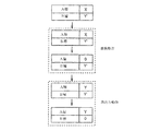
図3〜7は、突然の取出しがあった場合のカウンタ修復動作を、この突然の取出しが書込み位相、書込み位相と消去位相との間、又は消去位相のいずれで発生したかに従って示す。 3-7 show the counter repair operation in the event of a sudden fetch, depending on whether this sudden fetch occurred during the write phase, between the write phase and the erase phase, or the erase phase.
図3に示す第1状態においては、カードの突然の取出しは書込み位相で行われ、値Yは書込まれているが値Xは消去されていない。この場合、値Yは正しいが、この値のB層への保持は保証されない。したがって、値XをA層から消去してゼロに設定する前に、値Yは書換られる。メモリ位置への書込みは、そこにある値と新しい値との間のOR関数であるので、新しい値は古い値がゼロに等しいか新しい値と同一のとき(この場合に相当)にのみ書込みが可能であることに注意すべきである。 In the first state shown in FIG. 3, the card is suddenly removed at the write phase, the value Y is written but the value X is not erased. In this case, the value Y is correct, but retention of this value in the B layer is not guaranteed. Therefore, before erasing the value X from the A layer and setting it to zero, the value Y is rewritten. Writing to a memory location is an OR function between the value there and the new value, so the new value is only written when the old value is equal to zero or equal to the new value (in this case). Note that this is possible.
図4に示す第2状態においては、突然の取出しは書込み位相で行われており、B層にXとYとの間の値Y’が書込まれているが、値XはA層から消去されていない。この場合、第1書込み動作はB層へのY’の書換と、A層からのXの消去を実行する。次いで、書込み動作はA層へのYの書込みと、B層からのY’の消去を実行するので、カウンタは1つの層が新しい値を含み、別の層がゼロを含む正常な状態に戻る。 In the second state shown in FIG. 4, the sudden extraction is performed in the write phase, and the value Y ′ between X and Y is written in the B layer, but the value X is erased from the A layer. It has not been. In this case, in the first write operation, Y ′ is rewritten to the B layer and X is erased from the A layer. The write operation then performs a write of Y to the A layer and an erase of Y ′ from the B layer, so the counter returns to a normal state where one layer contains the new value and another layer contains zero. .
図5に示す第3状態においては、突然の取出しは書込み位相で行われており、B層にXより小さい値Y’が書込まれているが、値Xは消去されていない。この場合、第1書込み動作はA層へのXの書換とB層からのY’の消去を実行する。これは、カウンタの修復は常に最大値、この例ではX、を用いて実行されることをその根拠としている。次いで、書込み動作は、B層への値Yの書込みとA層からのXの消去を実行する。 In the third state shown in FIG. 5, the sudden extraction is performed in the write phase, and the value Y ′ smaller than X is written in the B layer, but the value X is not erased. In this case, the first write operation executes rewriting of X to the A layer and erasing of Y ′ from the B layer. This is based on the fact that counter repair is always performed using the maximum value, X in this example. Next, the write operation executes the writing of the value Y to the B layer and the erasure of X from the A layer.
図6に示す第4状態においては、突然の取出しは書込み位相と消去位相との間で行われ、B層には値Yが記録されているが値XはA層から消去されていない。この場合、値Yの保持は保証されないので、書換動作によりB層への値Yの書換とA層からのXの消去が実行される。 In the fourth state shown in FIG. 6, the sudden extraction is performed between the write phase and the erase phase, and the value Y is recorded in the B layer, but the value X is not erased from the A layer. In this case, since the retention of the value Y is not guaranteed, the value Y is rewritten to the B layer and the X is erased from the A layer by the rewriting operation.
図7に示す第5状態においては、突然の取出しが消去位相で行われ、B層に値Yは書込まれているが、値Xが正しく消去されずA層には値X’が見られる。したがって、B層への値Yの書換動作の実行が必要であり、その結果A層からの値X’の消去が可能になる。 In the fifth state shown in FIG. 7, the sudden extraction is performed in the erase phase, and the value Y is written in the B layer, but the value X is not erased correctly and the value X ′ is seen in the A layer. . Therefore, it is necessary to execute the rewriting operation of the value Y to the B layer, and as a result, the value X ′ from the A layer can be erased.
上述の状態すべてにおいて、2つの層のいずれにもゼロを含まない場合にカウンタの修復は行われ、修復後は、2つの層のうち一方は新しいデータ値を含み、他方はゼロを含む。どの状態においても、カウンタのA層又はB層に見られる最大値が古い値(X)より小さい状態にはならないことに注意すべきである。 In all of the above states, counter repair is performed if neither of the two layers contains zero, after which one of the two layers contains the new data value and the other contains zero. It should be noted that in any state, the maximum value found in the A or B layer of the counter is not less than the old value (X).
Claims (8)
各処理毎に、前記データ値の書込み動作は、前記メモリ内でデータ値としての値ゼロが記録された第1メモリ位置(B)と第2メモリ位置(A)とを持つカウンタの第1メモリ位置(B)に新しいデータ値(Y)の書込みを実行し、
前記書込み動作はまた前記第2メモリ位置(A)に記録されている古いデータ値(X)の消去を実行するようになっており、
その結果、前記書込み動作の最後に、その書込み動作が正しく実行された場合は、前記第1メモリ位置に新しいデータ値が記録され、前記第2メモリ位置には値ゼロが記録され、
処理の過程で前記スマートカードの突然の取出しがあった結果、前記書込み動作が正しく実行されない場合には、前記カウンタの前記第1、第2メモリ位置のどちらにも値ゼロが記録されない、ことを特徴とするカード処理システムにおけるデータの変更方法。 A smart card, the smart card in the card processing system including a readable reader to the smart card when in a predetermined positional relationship with respect to the reader, the smart card is directed to the processing executed by the smart card A method of changing data in a card processing system, comprising non-volatile, erasable and rewritable memory including at least one memory location for recording data values, each process resulting in an increase in said data value;
For each treatment, the write operation of the data values, a first memory counter having a first memory location (B) and the second memory location a value of zero as the data values stored in the memory (A) Write a new data value (Y) to position (B),
The write operation is also adapted to perform an erasure of the old data value (X) recorded in the second memory location (A);
As a result, the end of the write operation, if the write operation was successful, the new data value to the first memory location is recorded, the value zero is recorded in the second memory location,
Wherein in the course of the processing result there was a sudden extraction of the smart card, wherein when the write operation is not performed correctly, the first of said counter, to be the value zero which of the second memory location has a recorded, A method of changing data in a card processing system.
前記システムは、前記メモリが、カウンタを形成する所定の第1メモリ位置(B)と所定の第2メモリ位置(A)とを含み、
前記カウンタの前記データ値としての値ゼロが記録された第1メモリ位置(B)への新しいデータ値(Y)の書込みと、前記カウンタの他方の第2メモリ位置(A)からの古いデータ値(X)の消去とを実行する各処理の書込み命令の結果、
書込み動作の最後に、その書込み動作が正しく実行された場合は、前記第1メモリ位置(B)に新しいデータ値が記録され、前記第2メモリ位置(A)には値ゼロが記録され、
あるいは取引の過程で前記スマートカードの突然の取出しがあった結果、前記書込み動作が正しく実行されない場合には、前記カウンタの前記第1、第2メモリ位置のどちらにも値ゼロが記録されない、ことを特徴とするカード処理システム。Includes a smart card, and a readable reader to the smart card when the smart card is in a predetermined positional relationship with respect to the reader, the smart card, recorded data values relating to processing executed by the smart card A card processing system including a non-volatile, erasable and rewritable memory including at least one memory location for performing each processing, wherein each processing results in an increase in the data value;
The system includes a predetermined first memory location (B) and a predetermined second memory location (A) where the memory forms a counter;
Writing a new data value (Y) to the first memory location (B) where the value zero as the data value of the counter is recorded, and an old data value from the other second memory location (A) of the counter As a result of the write command of each process that executes erasure of (X),
At the end of the write operation , if the write operation is performed correctly, a new data value is recorded in the first memory location (B) , a value of zero is recorded in the second memory location (A) ,
Or result in the course of the transaction had a sudden extraction of the smart card, wherein when the write operation is not performed correctly, the first of said counter, to be the value zero which of the second memory location has a recorded card processing system, characterized in that,.
Applications Claiming Priority (2)
| Application Number | Priority Date | Filing Date | Title |
|---|---|---|---|
| FR0215740A FR2848702B1 (en) | 2002-12-12 | 2002-12-12 | SECURE METHOD FOR MODIFYING DATA RECORDED IN A MEMORY CARD |
| PCT/FR2003/003696 WO2004055741A2 (en) | 2002-12-12 | 2003-12-12 | Secure method for modifying data recorded in a memory card |
Publications (2)
| Publication Number | Publication Date |
|---|---|
| JP2006510099A JP2006510099A (en) | 2006-03-23 |
| JP4546256B2 true JP4546256B2 (en) | 2010-09-15 |
Family
ID=32338734
Family Applications (1)
| Application Number | Title | Priority Date | Filing Date |
|---|---|---|---|
| JP2004559826A Expired - Fee Related JP4546256B2 (en) | 2002-12-12 | 2003-12-12 | How to safely change the data recorded on the memory card |
Country Status (18)
| Country | Link |
|---|---|
| US (1) | US20060015675A1 (en) |
| EP (1) | EP1573690B1 (en) |
| JP (1) | JP4546256B2 (en) |
| KR (1) | KR20050088105A (en) |
| CN (1) | CN1757048A (en) |
| AT (1) | ATE404959T1 (en) |
| AU (1) | AU2003296828A1 (en) |
| BR (1) | BR0316935A (en) |
| CA (1) | CA2508119A1 (en) |
| DE (1) | DE60322949D1 (en) |
| FR (1) | FR2848702B1 (en) |
| IL (1) | IL168472A (en) |
| MX (1) | MXPA05006159A (en) |
| PT (1) | PT1573690E (en) |
| RU (1) | RU2353973C2 (en) |
| TW (1) | TW200424944A (en) |
| WO (1) | WO2004055741A2 (en) |
| ZA (1) | ZA200504256B (en) |
Families Citing this family (2)
| Publication number | Priority date | Publication date | Assignee | Title |
|---|---|---|---|---|
| US20090193527A1 (en) * | 2006-08-03 | 2009-07-30 | Freescale Semiconductor, Inc. | Method for monotonically counting and a device having monotonic counting capabilities |
| WO2008103870A1 (en) | 2007-02-23 | 2008-08-28 | Newpage Wisconsin System Inc. | Multifunctional paper identification label |
Family Cites Families (11)
| Publication number | Priority date | Publication date | Assignee | Title |
|---|---|---|---|---|
| JPH04344993A (en) * | 1991-05-22 | 1992-12-01 | Kyodo Printing Co Ltd | Non-contact type ic card |
| JPH05143468A (en) * | 1991-11-20 | 1993-06-11 | Toshiba Corp | Restoring device for power source turn-off |
| JPH05233426A (en) * | 1992-02-20 | 1993-09-10 | Fujitsu Ltd | Flash memory using method |
| JPH07248978A (en) * | 1994-03-11 | 1995-09-26 | Fuji Film Micro Device Kk | Nonvolatile memory |
| JPH0844832A (en) * | 1994-07-29 | 1996-02-16 | Citizen Watch Co Ltd | Non-contact portable storage medium processing system |
| US5778070A (en) * | 1996-06-28 | 1998-07-07 | Intel Corporation | Method and apparatus for protecting flash memory |
| JP3721725B2 (en) * | 1997-07-09 | 2005-11-30 | ソニー株式会社 | Information processing method and information processing apparatus |
| DE19756895C2 (en) * | 1997-12-19 | 2000-11-09 | Siemens Ag | Method for safely changing a value stored in a non-volatile memory and circuit arrangement therefor |
| JP2000099652A (en) * | 1998-09-25 | 2000-04-07 | Hitachi Ltd | Semiconductor recording media and recording and reproduction system using the same |
| JP2000357216A (en) * | 1999-06-15 | 2000-12-26 | Dainippon Printing Co Ltd | Ic card |
| DE19931184A1 (en) * | 1999-07-07 | 2001-01-11 | Bosch Gmbh Robert | Altering controller memory contents involves writing new data that is worthy of security into different memory area before transferring to original memory area contg. replaced data |
-
2002
- 2002-12-12 FR FR0215740A patent/FR2848702B1/en not_active Expired - Fee Related
-
2003
- 2003-12-08 TW TW092134544A patent/TW200424944A/en unknown
- 2003-12-12 RU RU2005121896/09A patent/RU2353973C2/en not_active IP Right Cessation
- 2003-12-12 KR KR1020057010284A patent/KR20050088105A/en not_active Application Discontinuation
- 2003-12-12 WO PCT/FR2003/003696 patent/WO2004055741A2/en active IP Right Grant
- 2003-12-12 JP JP2004559826A patent/JP4546256B2/en not_active Expired - Fee Related
- 2003-12-12 EP EP03813177A patent/EP1573690B1/en not_active Expired - Lifetime
- 2003-12-12 PT PT03813177T patent/PT1573690E/en unknown
- 2003-12-12 CN CNA2003801055923A patent/CN1757048A/en active Pending
- 2003-12-12 AT AT03813177T patent/ATE404959T1/en not_active IP Right Cessation
- 2003-12-12 CA CA002508119A patent/CA2508119A1/en not_active Abandoned
- 2003-12-12 MX MXPA05006159A patent/MXPA05006159A/en unknown
- 2003-12-12 BR BR0316935-9A patent/BR0316935A/en not_active Application Discontinuation
- 2003-12-12 DE DE60322949T patent/DE60322949D1/en not_active Expired - Fee Related
- 2003-12-12 US US10/534,975 patent/US20060015675A1/en not_active Abandoned
- 2003-12-12 AU AU2003296828A patent/AU2003296828A1/en not_active Abandoned
-
2005
- 2005-05-09 IL IL168472A patent/IL168472A/en active IP Right Grant
- 2005-05-25 ZA ZA200504256A patent/ZA200504256B/en unknown
Also Published As
| Publication number | Publication date |
|---|---|
| MXPA05006159A (en) | 2005-08-26 |
| BR0316935A (en) | 2005-10-18 |
| PT1573690E (en) | 2008-11-25 |
| ZA200504256B (en) | 2006-11-25 |
| WO2004055741A3 (en) | 2005-06-09 |
| CN1757048A (en) | 2006-04-05 |
| WO2004055741A2 (en) | 2004-07-01 |
| ATE404959T1 (en) | 2008-08-15 |
| EP1573690A2 (en) | 2005-09-14 |
| FR2848702B1 (en) | 2005-03-18 |
| IL168472A (en) | 2010-02-17 |
| US20060015675A1 (en) | 2006-01-19 |
| RU2005121896A (en) | 2006-01-20 |
| FR2848702A1 (en) | 2004-06-18 |
| EP1573690B1 (en) | 2008-08-13 |
| KR20050088105A (en) | 2005-09-01 |
| TW200424944A (en) | 2004-11-16 |
| DE60322949D1 (en) | 2008-09-25 |
| RU2353973C2 (en) | 2009-04-27 |
| JP2006510099A (en) | 2006-03-23 |
| CA2508119A1 (en) | 2004-07-01 |
| WO2004055741B1 (en) | 2005-09-15 |
| AU2003296828A1 (en) | 2004-07-09 |
Similar Documents
| Publication | Publication Date | Title |
|---|---|---|
| JP2514954B2 (en) | IC card | |
| US7725646B2 (en) | Method of using a flash memory for a circular buffer | |
| US5532463A (en) | Process for making secure the writing of sensitive data into the EEPROM data storage memory of a memory card and a memory card for use in the process | |
| JPH021090A (en) | Ic card and method for writing its operation program | |
| CN101645046A (en) | Emulation eines einmal programmierbaren speichers | |
| CN111104253B (en) | Smart card for power failure protection and working method thereof | |
| US11392449B2 (en) | Anti-tearing protection system for non-volatile memories | |
| CN111427726B (en) | IC card and anti-power-down data backup method or data recovery method thereof | |
| JP4546256B2 (en) | How to safely change the data recorded on the memory card | |
| CN101944191A (en) | Anti-prying treatment method of non-contact logic encryption card | |
| JP3195122B2 (en) | Check method of instruction format given to IC card | |
| US20070274302A1 (en) | Data Storage Device, Memory Managing Method, and Program | |
| JPS5977699A (en) | Integrated circuit card | |
| CN107402887B (en) | Counter in flash memory | |
| JP4211890B2 (en) | How to change memory card data in a transaction | |
| JP2528466B2 (en) | IC card | |
| JPS6215686A (en) | Method and apparatus for releasing user's memory | |
| JPH09223199A (en) | Ic card with counting function | |
| JP2609645B2 (en) | Portable electronic devices | |
| JPS63200399A (en) | Data processing system | |
| EP1344224A2 (en) | Method for the secure updating of data areas in a non volatile memory and device to perform such a method | |
| JP2013003831A (en) | Ic chip, processing program for ic chip, and writing processing method in ic chip | |
| JP3054119B2 (en) | Portable electronic devices | |
| JPS63229542A (en) | Electronic card | |
| JPH01180688A (en) | Portable electronic device |
Legal Events
| Date | Code | Title | Description |
|---|---|---|---|
| A621 | Written request for application examination |
Free format text: JAPANESE INTERMEDIATE CODE: A621 Effective date: 20061205 |
|
| A977 | Report on retrieval |
Free format text: JAPANESE INTERMEDIATE CODE: A971007 Effective date: 20091028 |
|
| A131 | Notification of reasons for refusal |
Free format text: JAPANESE INTERMEDIATE CODE: A131 Effective date: 20091117 |
|
| A601 | Written request for extension of time |
Free format text: JAPANESE INTERMEDIATE CODE: A601 Effective date: 20100215 |
|
| A602 | Written permission of extension of time |
Free format text: JAPANESE INTERMEDIATE CODE: A602 Effective date: 20100222 |
|
| A601 | Written request for extension of time |
Free format text: JAPANESE INTERMEDIATE CODE: A601 Effective date: 20100316 |
|
| A521 | Request for written amendment filed |
Free format text: JAPANESE INTERMEDIATE CODE: A523 Effective date: 20100326 |
|
| A602 | Written permission of extension of time |
Free format text: JAPANESE INTERMEDIATE CODE: A602 Effective date: 20100329 |
|
| TRDD | Decision of grant or rejection written | ||
| A01 | Written decision to grant a patent or to grant a registration (utility model) |
Free format text: JAPANESE INTERMEDIATE CODE: A01 Effective date: 20100615 |
|
| A01 | Written decision to grant a patent or to grant a registration (utility model) |
Free format text: JAPANESE INTERMEDIATE CODE: A01 |
|
| A61 | First payment of annual fees (during grant procedure) |
Free format text: JAPANESE INTERMEDIATE CODE: A61 Effective date: 20100701 |
|
| FPAY | Renewal fee payment (event date is renewal date of database) |
Free format text: PAYMENT UNTIL: 20130709 Year of fee payment: 3 |
|
| R150 | Certificate of patent or registration of utility model |
Free format text: JAPANESE INTERMEDIATE CODE: R150 |
|
| R250 | Receipt of annual fees |
Free format text: JAPANESE INTERMEDIATE CODE: R250 |
|
| R250 | Receipt of annual fees |
Free format text: JAPANESE INTERMEDIATE CODE: R250 |
|
| R250 | Receipt of annual fees |
Free format text: JAPANESE INTERMEDIATE CODE: R250 |
|
| LAPS | Cancellation because of no payment of annual fees |