JP4545854B2 - Projection exposure equipment - Google Patents
Projection exposure equipment Download PDFInfo
- Publication number
- JP4545854B2 JP4545854B2 JP31561199A JP31561199A JP4545854B2 JP 4545854 B2 JP4545854 B2 JP 4545854B2 JP 31561199 A JP31561199 A JP 31561199A JP 31561199 A JP31561199 A JP 31561199A JP 4545854 B2 JP4545854 B2 JP 4545854B2
- Authority
- JP
- Japan
- Prior art keywords
- light
- illuminance
- optical
- illumination
- exposure apparatus
- Prior art date
- Legal status (The legal status is an assumption and is not a legal conclusion. Google has not performed a legal analysis and makes no representation as to the accuracy of the status listed.)
- Expired - Fee Related
Links
Images


Description
【0001】
【発明が属する技術分野】
本発明は投影露光装置に関し、特に、半導体素子等の製造に用いられる投影露光装置の照明装置部分に関し、照明条件や照明モードを変更した場合の被照射面上の照度の均一化および各機体毎の照度分布の補正に有効な技術である。
【0002】
【従来の技術】
半導体素子製造用の投影露光装置では、照明系からの光束で電子回路パターンを形成したレチクルを照射し、該パターンをウエハー面上に露光する。この際、高解像力化を図るための一要件としてウエハー面上を均一に照射することが好ましい。
【0003】
この種の投影露光装置で用いられる照明系では、照射面を均一に照射するための種々の方法が知られている。例えば、一般にステッパーと呼ばれる投影露光装置では、コリメータレンズと複数の微小レンズを所定のピッチで配列したオプティカルインテグレータとを組み合わせた照明系を用いて、被照射面を均一に照射している。
【0004】
照明系に、このようなオプティカルインテグレータを用いることにより、微小レンズの個数に相当するだけの複数の2次光源を形成でき、2次光源からの光束で被照射面を複数の方向から重畳して、照度分布の均一化を図っている。
【0005】
一般に被照射面での照度不均一性を示す値として、照度ムラSを、被照射面での照度値の最大値をSmax、最小値をSminとして、
S=(Smax−Smin)/(Smax+Smin)
で表現するが、上記のような構成によって該被照射面での不均一性を数パーセント以内にすることができる。
【0006】
【発明が解決しようとする課題】
しかしながら、最近の超LSIの高集積化に伴い、回路パターンの焼き付けに要求される照度均一性は±1%前後という極めて高いものとなり、上記の技術のみでは不十分になってきている。
【0007】
また解像度を高めるために、斜入射照明や位相シフトマスクと呼ばれる超解像結像技術が提案されている。このような照明法では、照明光学系の開口絞りを変更することでσ値を小さくしたり、輪帯形状や四重極形状のような特殊な形状の2次光源を形成している。
【0008】
このような複数の照明方法に対し、多くの投影露光装置ではある標準的な照明モードAで照度ムラが最小になるように照明系の各要素の位置を調整している。しかしながら、斜入射照明法や小σ値等の照明モードBに変えたときには、照明系の各要素が照明モードAと同じでは必ずしも照明ムラが最小とはならない。
【0009】
投影露光装置においては照明モードを切り替えると、光路が異なって来るため、光学素子に用いられている反射防止膜の効果が光線の角度により異なったり、ミラーによる折り返しでの反射ムラや光学系の偏心の影響や、ウエハー面、レチクル面、投影光学系、照明光学系の間で生じる反射によって生じるフレアの影響が異なってくるため、被照射面に照度ムラが発生していた。このような照度ムラを照明条件切替時に補正することは従来の露光装置では困難であった。
【0010】
また反射防止膜の成膜状態や組立精度などにより、組み立てられた露光装置は各機体固有の局所的な照度ムラを持っており、これらを補正することも従来の露光装置では困難であった。
【0011】
そこで、本発明は、照明条件を変更した際に生じる照度ムラを最小とするとともに、各機体固有の照度ムラを補正し、レチクル面上の各種のパターンをウエハー面上に高い解像力で投影することを課題としている。
【0012】
【課題を解決するための手段】
上記の課題を解決するための本発明は、光源からの光で被照射面上に配置したレチクルを照明する照明系と、前記レチクルのパターンを基板上に投影する投影光学系と、を備える投影露光装置において、前記照明系は、複数の微小レンズを含むオプティカルインテグレータと、前記複数の微小レンズに入射する前記光源からの光の光量を前記微小レンズ毎に調整する複数の第1光量調整部を含み、駆動機構により前記照明系の光軸と直交する平面内を移動する駆動光学フィルターと、前記複数の微小レンズに入射する前記光源からの光の光量を前記微小レンズ毎に調整する複数の第2光量調整部を含み、前記照明系の光軸と直交する平面内で固定された固定光学フィルターと、を有し、前記駆動光学フィルターは、前記被照射面上における照度ムラのうち、他の照明モードに変更したときに生じる照度ムラを補正し、前記固定光学フィルターは、前記被照射面上における照度ムラのうち、照明モードを問わず一定の傾向の照度ムラを補正する。
【0013】
【発明の実施の形態】
以下、図面を参照して、本発明の実施の形態について説明する。
【0014】
(実施形態1)
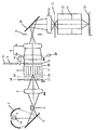
図1は本発明の投影露光装置の光路図である。1は水銀ランプ等の光源としての発光管であり、紫外線及び遠紫外線等を放射する高輝度の発光部1aを有している。発光部1aは楕円ミラー2の第1焦点近傍に配置している。1aはその第2焦点4に結像される。3はコールドミラーであり、多層膜より成り、大部分の赤外光を透過すると共に大部分の紫外線を反射させている。楕円ミラー2はコールドミラー3を介して第2焦点4近傍に発光部1aの発光部像(光源像)1bを形成している。
【0015】
5は光学系であり、コンデンサーレンズやコリメータレンズそしてズームレンズなどから成り、第2焦点4近傍に形成した発光部像1bを、光量制御手段17を介して、オプティカルインテグレータ6の入射面6aに結像させている。
【0016】
オプティカルインテグレータ6は断面が4角形状の複数の微小レンズ6cを2次元的に所定のピッチで配列して構成しており、その射出面6b近傍に2次光源を形成している。
【0017】
駆動光量制御手段17は光軸上に垂直な平面に沿って2次元的に移動可能で、オプティカルインテグレータ6の光射出面6a近傍に配置している。駆動光量制御手段17はオプティカルインテグレータ6の複数の微小レンズ6cのうち少なくとも1つの微小レンズを透過する光量を、NDフィルターや遮光部材から成る光量調整部により制御している。
【0018】
18はホルダーであり、図示しない照度分布測定手段からの信号に基づいて駆動光量制御手段17を光軸に垂直な平面に沿って2次元的に移動、あるいは光軸方向へ直線的に移動させて被照射面10上の照度分布を調整している。
【0019】
固定光量制御手段19もオプティカルインテグレータ6の光射出面6a近傍に配置されており、駆動光量制御手段17と同様オプティカルインテグレータ6の複数の微小レンズ6cのうち少なくとも1つの微小レンズを透過する光量をNDフィルターや遮光部材から成る光量調整部を持っている。
【0020】
7は絞りであり、2次光源の形状を決定している。絞り7は照明条件に応じて絞り交換機構(アクチュエータ)16によって種々の絞り7a,7bが光路中に位置するように切り替え可能となっている。絞り7としては、例えば通常の円形開口の絞りや、後述する投影レンズ13の瞳面14上の光強度分布を変化させる輪帯照明用絞り、4重極照明用絞り、小σ値照明用絞り等から成っている。本実施形態では種々の絞り7を用いることにより、集光レンズ8に入射する光束を種々と変えて投影光学系13の瞳面14上の光強度分布を適切に制御している。
【0021】
集光レンズ8はオプティカルインテグレータ6の射出面6b近傍の2次光源から射出し、絞り7を透過した複数の光束を集光し、被照射面としてのマスキングブレード10面を均一に照射している。また集光レンズ8はズームレンズ8aと固定レンズ8bから構成されており、ズームレンズ駆動機構20によりズームレンズ8aを光軸方向に移動させることで、実質的に焦点距離を変えないようにしつつ、ディストーションを変化させる機構になっている。
【0022】
マスキングブレード9は複数の可動の遮光板より成り、任意の開口形状が形成されるようにしている。
【0023】
10はミラー、11は結像レンズであり、マスキングブレード9の開口形状を被照射面としてのレチクル12面に転写し、レチクル12面上の必要な領域を均一に照明している。13は投影光学系(投影レンズ)であり、レチクル12面上の回路パターンをウエハーチャックに載置したウエハー(基板)15面上に縮小投影している。14は投影光学系の瞳である。
【0024】
本実施形態における光学系では、発光部1aと第2焦点4とオプティカルインテグレータ6の入射面6aとマスキングブレード9とレチクル12とウエハー面15とが共役である。また、絞り7と投影光学系13の瞳面14とは、ほぼ共役である。
【0025】
本実施形態では、レチクル面12面上のパターン形状に応じて開口形状の異なった絞りを選択して用いて、投影光学系13の瞳面14に形成される光強度分布を種々と変えている。
【0026】
次に本実施形態の駆動光量制御手段17の光学的作用について説明する。
【0027】
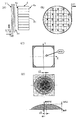
図2(A)は、駆動光量制御手段17の光量調整部としてNDフィルター(または遮光部材)を用いた光学フィルターの光入射側から見た概略図である。光学フィルター17および光学フィルター19はオプティカルインテグレータ6を構成する複数の微小レンズ6cに各々対応していて、複数の領域の透過光量が調整できる光量調整部を有している。光学フィルター17においてオプティカルインテグレータ6の複数の微小レンズに対応して、入射光量を減少させる円形状のNDフィルター31による光量調整部を示している。このNDフィルター31には大きさの異なる2種類のものがある。
【0028】
図2(B)は光量制御手段(光学フィルター)17とオプティカルインテグレータ6の側面図である。6cはオプティカルインテグレータ6を構成する複数の微小レンズである。微小レンズ6cの光入射側のレンズ面6aの後側焦点は光射出側のレンズ面6bの位置にある。また、微小レンズ6cの光射出側のレンズ面6bの前側焦点は光入射側のレンズ面6aの位置にある。この為、光学系5で微小レンズ6cのレンズ面6aに集光した光束はレンズ面6bより平行光束として射出している。そしてレンズ面6bから射出した平行光束は絞り7aを介し、集光レンズ8で集光されミラー9で反射してマスキングブレード10上に集光している。このようにしてオプティカルインテグレータ6の光入射面6aとマスキングブレード10とを共役関係になるようにしている。
【0029】
オプティカルインテグレータ6の光入射面6aとレチクルもしくはウエハ等の被照射面は光学的に共役である。照度ムラを補正する光学フィルター17,19はオプティカルインテグレータ6の入射面6aから所定間隔Dの位置に配置されており、Dが大きくなるに従ってNDフィルターによる照度低下部分とそうでない部分との境界が不鮮明になり、被照射面上(ウエハー15)での照度分布変化の断面は矩形ではなく、なだらかな形状で照度低下を起こす。
【0030】
本実施形態では光学フィルター17に大きさの異なる円形状のNDフィルターを配し、各NDフィルター部分に図3(A),(B)のような効果を持たせている。各NDフィルターの径や透過率、配置を適切にすることで、最終的に被照射面では図3(A),(B)の総和である図3(C)のように近似的に像高の2乗に比例して周辺の照度を上げる作用を有している。
【0031】
図3(C)に示された照度向上作用を、像高のほぼ二乗に比例して周辺部の照度を上げるとともに、最大像高での照度を軸上よりもaだけ高くする作用とする場合には、、たとえば図3(A)では最大像高の半分の位置から最大像高に至るまで(3/4)×aの照度差が生じるように、又、図3(B)では軸上から最大像高の半分の位置に至るまで(1/4)×aが生じるように、NDフィルタの大きさ・パターン配置・透過率を定めるとよい。
【0032】
一般に投影露光装置の照明装置において、被照射面における開口数の均一性と照度分布の均一性を両立させようとすると、オプティカルインテグレータ6の正弦条件不満足量、およびレンズに用いられる反射防止膜の角度特性により周辺の照度が低下する傾向にある。そのため、本実施形態のように周辺の照度を上げる作用を有する光学フィルターは照度分布の補正に有効である。
【0033】
一般にオプティカルインテグレータに入射する光束は、光軸に対して対称な照度分布を持つように調整してある。これにより、被小斜面での有効光源分布は主光線に対して対称になるため、デフォーカスに対して像のズレが生じない。ひいては、良好なテレセン度での露光を実現している。
【0034】
仮に、オプティカルインテグレータに入射する光束は、光軸に対して非対称な照度分布を持つ場合には、有効光源分布の対称性が失われ、テレセン度のズレという形で像性能へ影響が及ぶが、この実施形態では、光軸対称に小レンズの光量を調整しているのでテレセン度のズレがほとんど生じない。このようにNDフィルター17の透過率調整部の形状、大きさ、透過率、距離Dを適切に決めることによって、被照射面全域に渡って照度分布を均一に調整している。
【0035】
以下、照度ムラの補正を具体例に即して説明する。照明モードAでは図4(A)、照明モードBでは図5(A)のような照度ムラが有るものとする。相対照度は、階調で表現されており、相対照度の等高線は0.5%刻みである。更に、各領域の相対照度は、96.0%から101.5%であり、それを数字で示してある。又、格子線は、被照射面の各点に座標を与えるためのものである。
【0036】
発生した照度ムラはそれぞれ図4(B)(C)(D)及び図5(B)(C)(D)のような、傾斜状の照度ムラ(B)と、同心円上の光軸対称な周辺照度が下がった照度ムラ(C)、および局所的なその他の成分(D)に分解することができる。これらは照度分布から像高別平均照度および傾斜成分を放出することより、容易に分離できる。図4(A)、図5(A)の照度ムラを、それぞれ図4(B)(C)、図5(B)(C)のように分解して残ったムラ成分が、それぞれ図4(D)、図5(D)である。照明モード固有の照度ムラを補正した後の図4(D)及び図5(D)のムラ成分は同じものである。
【0037】
以下、このように成分に分けた照度ムラの補正方法を述べる。
【0038】
まず、図4及び図5のパターン(B)の傾斜状の照度ムラの補正方法について図6及び図7を参照して説明する。前述したように本実施形態の光学フィルター17は像高のほぼ2乗に比例して周辺部の照度分布をあげる効果を持つ。このとき、オプティカルインテグレータ6の微小レンズの有効径をウエハ・レチクルの被照射面相当とし、オプティカルインテグレータ6の微小レンズ有効径の入射面を正規化されたXY座標系とすれば、光学フィルター17の効果zは
z=a(x2+y2)と書ける。ここで、aは定数である。
【0039】
このため、光学フィルター17を光軸に垂直な平面に沿って2次元的に移動させることにより、1次元的に傾斜状の照度分布変化を発生させることができる。
【0040】
実際には、照明モード毎に光学フィルター17の効き率が若干異なるので、この実施形態では、図6のフローチャートで示すように光学フィルター17の効き率を算出して傾斜状照度ムラの補正を行う。具体的には、図4に関してはa=3.0、図5に関してはa=4.0の効果を持つように、光学フィルター17を設定すればよい。
【0041】
図7(A)(B)はNDフィルター17の移動方向を示している。被照射面での周辺部4点、すなわち図7(C)の網掛け部の照度を予め測定し、基礎データとして用いる。図7(A)(B)のように光軸に垂直な平面に沿ってX座標およびY座標を取る。NDフィルター17をX方向、Y方向に所定距離d0移動させて照度ムラ測定を行い、被照射面での周辺部4点の照度の変化量を装置の図示しない演算装置によって計算し、NDフィルター17を移動させたときの変化量の効き率を装置の図示しない記憶装置に記憶させる。この効き量を基にNDフィルター17を動かすべき方向と量を演算装置によって計算する。
【0042】
この演算結果に基づいて光学フィルター駆動機構18によりフィルター17を所定方向へ所定量駆動させる。駆動後再度照度ムラ測定を行い、最適値になっていたら終了、さらに最適にする余地がある場合には、上記の作業を繰り返して非対称ムラを最適に補正する。この手順におけるフィルター17による照度ムラ補正範囲の変化の例を図7(D)に示している。
【0043】
次に、図4及び図5のパターン(C)、すなわち光軸対称な照度ムラの補正方法について図8及び図9を参照して説明する。光軸対称な照度ムラが発生した場合は、周辺照度補正量を調整することになるが、NDフィルターまたは遮光部材を光軸方向に直線的に移動させてオプティカルインテグレータの入射面との距離Dを大きくし、被照射面上での照度低下の割合を小さくすることを可能としている。また、NDフィルターまたは遮光部材と、オプティカルインテグレータの入射面との距離を調整することにより、光量調整部分の形状をぼかして照度調整範囲の大きさを調整するようにしている。
【0044】
被照射面最周辺部4点、すなわち、図9(B)の網掛け部の照度と中心から最周辺部の例えば50%部4点の照度を予め測定し、基礎データとして用いる。装置の図示しない記憶装置には、NDフィルター17を光軸方向に所定距離D0移動させて照度ムラを測定し、被照射面最周辺部4点の照度と中心から最周辺部の50%部4点の照度の変化量を装置の図示しない演算装置によって計算し、NDフィルター17を移動させたときの変化量の効き率を装置の記憶装置に記憶させる。この効き量をもとにNDフィルター17を光軸方向に動かすべき方向と量を装置の演算装置によって計算する。補正する範囲を大きくしたい場合は距離Dを増加させる方向に、小さくしたい場合は距離Dを小さくすればよい。この演算結果に基づいて光学フィルター駆動機構18によりフィルター17を所定方向へ所定量駆動させ、補正範囲の調整を行う。駆動後再度照度ムラ測定を行い、最適値になっていたら終了、さらに最適にする余地がある場合には、上記の作業を繰り返して照度ムラを最適に補正する。この手順における照度ムラ補正範囲の変化の例を図9(C)(D)に示している。
【0045】
NDフィルター17の移動方向が光軸に垂直な平面内に沿っている場合と、光軸方向である場合の両方について説明したが、これらを両方行うことによってより細やかな補正ができることは言うまでもない。この場合は図6と図8で示したフローチャートを直列的に実行したり、並列的に実行するようにすればい。
【0046】
NDフィルター17の移動により照度ムラの最適化を行った際には、図6と図8で示した実行結果(NDフィルター17位置)を記憶装置(不図示)に記憶しておく。その後、同一照明条件を再度実行する際には、実行結果を呼び出して最適位置に駆動させれば、図6・図8のような手順を踏むことなく、速やかに同心円状の照度ムラおよび傾斜状の照度ムラの最適化を行える。
【0047】
次に、図4及び図5のパターン(D)の照度ムラ、すなわち投影露光装置固有の局所的な照度ムラの補正方法について図1を参照して説明する。
【0048】
投影露光装置においては、被照射面(ウエハー面15)および光学的共役面(レチクル面12、マスキングブレード面9)の近傍のガラス部材などに、反射防止膜の膜ムラ、付着物などが発生すると、照明モードを問わず一定の傾向の照度ムラが発生するが、一般的にこの照度ムラは機体毎に異なる。
【0049】
これを補正するため、前述の駆動光量制御手段17と同じような構造を持った光量制御手段19をオプティカルインテグレータの入射面に備えている。各照明モードでの照度ムラ計測結果より、各機体固有の照度ムラを抽出し、これを補正するように、固定光量制御手段19にNDフィルターを構成する。固定光量制御手段19が被照射面での照度分布を制御する作用は駆動光量制御手段17と同様であって、設けられたNDフィルターにより各機体固有の照度ムラを補正している。
【0050】
この各機体固有の照度ムラは照明モードを問わず傾向が同一であるため、オプティカルインテグレータの入射面側に固定的に備えられれば良い。駆動機構を省くことによって、装置の簡略化が可能となる。
【0051】
この固定光量制御手段19を各機体毎に設定することにより、機体毎に異なる固有照度ムラを良好に補正することができる。固有照度ムラが十分に小さい場合は固定光量制御手段19の構成を省くことも可能である。この際も固定光量制御手段19は平行平面な光学材料で構成されているため、光学性能が変わってしまうことがない。
【0052】
ただし、駆動光量制御手段17のNDフィルターと固定光量制御手段19のNDフィルターは、オプティカルインテグレータ6の同一微小レンズの入射光量を制御しないよう設定する方がよい。複数のNDフィルターがオプティカルインテグレータ6の同一微小レンズに影響すると、補正効果の算出や補正形状の変化が複雑になるし、NDフィルター相互で悪影響を及ぼす可能性もあるからである。
【0053】
(実施形態2)
実施形態1においては光軸対称な照度ムラの補正するのに、NDフィルター(または遮光部材)を光軸方向に直線的に移動させたが、次のような方法も考えられる。
【0054】
集光レンズ8は駆動レンズ8aと固定レンズ8bから構成されており、駆動レンズ駆動機構20により駆動レンズ8aを光軸方向に移動させることで、実質的に焦点距離を変えないようにしつつ、ディストーションを変化させる機構になっている。この作用により、レンズ駆動することで、周辺照度を上下させることが可能となっている。
【0055】
この実施形態における周辺照度を変化させる手順を図10のフローチャートで示す。図11(A)は駆動レンズ8aの移動方向を示している。
【0056】
被照射面最周辺部4点の照度と中心から最周辺部の例えば50%部4点の照度を予め測定し、基礎データとして用いる(図9(B)の網掛け部)。装置の記憶装置(不図示)には、ズームレンズ8aを光軸方向に所定距離D0移動させたときの、被照射面最周辺部4点の照度と中心から最周辺部の50%部4点の照度の効き量を装置の記憶装置(不図示)に記憶させてある。この効き量はシミュレーション等により前もって求めることができる。この効き量をもとにズームレンズ8aを光軸方向に動かすべき方向と量を装置の演算装置(不図示)によって計算する。この演算結果に基づいて駆動機構20によりズームレンズ8aを所定方向へ所定量駆動させ、周辺照度の調整を行う。駆動後再度照度ムラ測定を行い、最適値になっていたら終了、さらに最適にする余地がある場合には、上記の作業を繰り返して照度ムラを最適に補正する。
【0057】
実施形態2の場合も、NDフィルター17を光軸に垂直な平面内に沿って移動する場合と、上に示したレンズ駆動を両方行うことによってより細やかな補正ができることは言うまでもない。この場合は図6と図10で示したフローチャートを直列的に実行したり、並列的に実行するようにすればよい。
【0058】
NDフィルター17およびレンズ8aの移動により照度ムラの最適化を行った際には、図6と図10で示した実行結果を記憶装置(不図示)に記憶しておく。その後、同一照明条件を再度実行する際には、実行結果を呼び出して各要素を最適位置に駆動させれば、図6・図10のような手順を踏むことなく、速やかに同心円状の照度ムラおよび傾斜状の照度ムラの最適化を行える。
【0059】
以上、本発明の2つの実施の形態について説明したが、本発明はこれに限定されるものではない。
【0060】
本実施形態と同様に像高ほぼ2乗に比例して周辺の照度を上げる作用を有していれば、図2に示した形態以外のフィルターを適用できる。たとえば、本実施形態では、簡単のため2種類の大きさのNDフィルターにより2次近似的に周辺光量を上げる作用を持つフィルターを示したが、3種類以上の大きさのNDフィルターの組み合わせによって、より2次曲線に近似したフィルターを構成することもできる。
【0061】
その他にも、図12に示すように、各オプティカルインテグレータの微小レンズに対して、中心部から連続的に透過率を変化させるフィルターが考えられる。
【0062】
本実施形態に倣って、図2、12に示すように、NDフィルターの透過率を最適化しつつ、透過率調整部を多数配置すれば、通常照明とその他の輪帯照明や4重極照明、あるいは位相シフトマスクの際に用いられるσ値が小さい照明条件等、多数の照明モードに関しても同様の機能を持たせることができる。
【0063】
このような多数のパターン配置を行う場合、テレセン度のずれを極小にするため、透過率調整部は中心あるいは中心回転対称に正方形の4つの頂点に位置するように設けてあり、さらに中心から同一距離にある透過率調整部の透過率は等しくなるようにしている。
【0064】
また、斜入射照明法や小σ値での照明は通常照明に比較して、重畳されるオプティカルインテグレータ6からの光束は少なくなる。このことからオプティカルインテグレータ6の微小レンズ1つあたりの被照射面での寄与率が大きくなるため、NDフィルターの透過率の選定には注意を要する。
【0065】
本実施形態のNDフィルターや遮光部材は一般にガラス基板面上にCr等の金属膜や誘電体多層膜を蒸着したり、または基板そのものに色素を混ぜたりして所望の透過率が得られるように構成している。尚、NDフィルターと同様の光学的性質を有するものであれば、他の光学部材を用いても良い。
【0066】
又、上述した照度ムラ補正方法は他の照明モードに変更したときに生じた照度ムラに限らず、経時的変化等で照度ムラが生じたときにも同様に用いることができる。
【0067】
また、図6のフローチャートにおいて、効き率の算出に最周辺部4点とは別の点を使用したり、図8、図10のフローチャートで像高50%部分の照度をデータとして使用しているのを、像高30%や70%等での照度をデータとして用いる等して、補正を最適化できるようにしてあることが望ましい。
【0068】
本実施形態の投影露光装置では、有効光源形成のための光源として水銀ランプを用いているが、レーザー等による有効光源形成も本実施形態と何ら機構的に異なるものではない。
【0069】
次に、本発明の投影露光装置を用いる半導体デバイスの製造方法について説明する。
【0070】
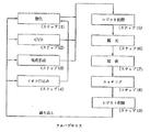
図13は、半導体デバイス(ICやLSI等の半導体チップ、液晶パネルやCCD)の製造工程を説明するためのフローチャートである。
【0071】
ステップ1の回路設計工程においては、半導体デバイスの回路設計を行う。ステップ2のマスク制作工程においては、設計した回路パターンを形成したマスク、すなわちレチクル12を作製する。一方、ステップ3のウエハ製造工程においては、シリコン等の材料を用いてウエハ15を製造する。ステップ4のウエハプロセス工程(前工程)においては、用意したレチクル12とウエハ15とを用いて、リソグラフィーによってウエハ15上に実際の回路を形成する。ステップ5の組立工程(後工程)においては、ステップ4で作成されたウエハ15をチップ化する。具体的には、ダイシング、ボンディング、パッケージング等が行われる。ステップ6の検査工程においては、ステップ5で作成された半導体デバイスの動作確認テスト、耐久性試験等の検査が行われる。ステップ7においては、こうして完成した半導体デバイスが出荷される。
【0072】
図14は、図13に示したステップ4、すなわちウエハプロセス工程(前工程)を説明するためのフローチャートである。
【0073】
ステップ11の酸化工程では、ウエハ15の表面を酸化させる。ステップ12のCVD工程では、CVD(化学気相成長)によってウエハの表面に絶縁膜を形成する。ステップ13の電極形成工程では、ウエハ15条に電極を蒸着等によって形成する。ステップ14のイオン打ち込み工程では、ウエハ15にイオンを打ち込む。ステップ15のレジスト処理工程では、ウエハにレジスト、すなわち感光材料を塗布する。ステップ16の露光工程では、本発明の露光投影装置によって、レチクル12の回路パターンの像でウエハ15を露光する。ステップ17の現像工程では、露光したウエハを現像する。ステップ18のエッチング工程では、現像したレジスト以外の部分を除去する。ステップ19のレジスト隔離工程ではエッチングが済んで不要となったレジストを取り除く。これらのステップを繰り返すことによってウエハ上に回路パターンが形成される。
【0074】
このような、本発明の半導体デバイスの製造方法によって、従来は困難であった高集積度の半導体デバイスを製造する。
【0075】
【発明の効果】
以上説明した本発明によれば、照明モードを変更した際に生じる照度ムラ、および各機体固有の照度ムラが効果的に補正され、オプティカルインテグレータを用いた投影露光装置において照度均一性に優れた照明が可能になる。すなわち、種々の照明モード、各機体において照度ムラを最小とし、レチクル面上の各種のパターンをウエハー上に安定して高い解像力で投影することができる。
【図面の簡単な説明】
【図1】本発明の投影露光装置の光路図
【図2】NDフィルターとオプティカルインテグレータの位置関係を示す図
【図3】被照射面での照度分布の変化特性例を示す図
【図4】照明モードAにおける照度ムラを示す図
【図5】照明モードBにおける照度ムラを示す図
【図6】NDフィルターを光軸に垂直な平面に沿って移動させたときの照度ムラ補正手順を示すフローチャート
【図7】NDフィルターを光軸に垂直な平面に沿って移動させたときの照度ムラ補正手順を説明するための図
【図8】NDフィルターを光軸に沿って移動させたときの照度ムラ補正手順を示すフローチャート
【図9】NDフィルターを光軸に沿って移動させたときの照度ムラ補正手順を説明するための図
【図10】駆動レンズを光軸に沿って移動させたときの照度ムラ補正手順を示すフローチャート
【図11】駆動レンズを光軸に沿って移動させたときの照度ムラ補正手順を説明するための図
【図12】光学フィルターの別の例を示す図
【図13】半導体デバイスの製造工程を説明するためのフローチャート
【図14】図13におけるウエハプロセスを説明するためのフローチャート
【符号の説明】
1 水銀ランプ(光源)
2 楕円ミラー
3 コールドミラー
4 楕円ミラー2の第2焦点
5 ズームレンズ
6 オプティカルインテグレータ
7 絞り
8 コンデンサーレンズ
8a 駆動レンズ
8b 固定レンズ
9 マスキングブレード
10 ミラー
11 レンズ
12 レチクル
13 投影光学系(投影レンズ)
14 投影レンズ瞳
15 ウエハー
16 絞り交換機構
17 駆動光量制御手段(光学フィルター)
18 光学フィルター駆動機構
19 固定光量制御手段(光学フィルター)
20 レンズ駆動機構
31 NDフィルター[0001]
[Technical field to which the invention belongs]
The present invention relates to a projection exposure apparatus, and more particularly to an illumination apparatus portion of a projection exposure apparatus used for manufacturing semiconductor elements and the like, and uniformizing illuminance on a surface to be irradiated when changing illumination conditions and illumination modes and for each body. This is an effective technique for correcting the illuminance distribution.
[0002]
[Prior art]
In a projection exposure apparatus for manufacturing semiconductor elements, a reticle on which an electronic circuit pattern is formed is irradiated with a light beam from an illumination system, and the pattern is exposed on a wafer surface. At this time, it is preferable to uniformly irradiate the wafer surface as one requirement for achieving high resolution.
[0003]
In an illumination system used in this type of projection exposure apparatus, various methods for uniformly irradiating an irradiation surface are known. For example, in a projection exposure apparatus generally called a stepper, an irradiated surface is uniformly irradiated using an illumination system in which a collimator lens and an optical integrator in which a plurality of minute lenses are arranged at a predetermined pitch.
[0004]
By using such an optical integrator in the illumination system, it is possible to form a plurality of secondary light sources corresponding to the number of microlenses, and to superimpose the illuminated surface from a plurality of directions with light beams from the secondary light sources. The illuminance distribution is made uniform.
[0005]
In general, as a value indicating illuminance non-uniformity on the irradiated surface, the illuminance unevenness S, the maximum value of the illuminance value on the irradiated surface as Smax, and the minimum value as Smin,
S = (Smax−Smin) / (Smax + Smin)
However, the non-uniformity on the irradiated surface can be made within several percent by the configuration as described above.
[0006]
[Problems to be solved by the invention]
However, with the recent high integration of VLSI, the illuminance uniformity required for baking circuit patterns has become extremely high of about ± 1%, and the above-described technology alone is insufficient.
[0007]
In order to increase the resolution, super-resolution imaging techniques called oblique incidence illumination and phase shift masks have been proposed. In such an illumination method, the σ value is reduced by changing the aperture stop of the illumination optical system, or a secondary light source having a special shape such as an annular shape or a quadrupole shape is formed.
[0008]
For such a plurality of illumination methods, the position of each element of the illumination system is adjusted so that the illuminance unevenness is minimized in a certain standard illumination mode A in many projection exposure apparatuses. However, when changing to the illumination mode B such as the oblique incidence illumination method or the small σ value, the illumination unevenness is not necessarily minimized if each element of the illumination system is the same as the illumination mode A.
[0009]
When switching the illumination mode in a projection exposure apparatus, the optical path changes, so the effect of the antireflection film used in the optical element varies depending on the angle of the light beam, reflection unevenness due to mirror folding, and eccentricity of the optical system. The illuminance unevenness occurs on the surface to be irradiated because the influence of the flare caused by the reflection and the flare caused by the reflection generated between the wafer surface, the reticle surface, the projection optical system, and the illumination optical system are different. It has been difficult for a conventional exposure apparatus to correct such illuminance unevenness when switching illumination conditions.
[0010]
Further, the assembled exposure apparatus has local illuminance unevenness unique to each machine depending on the film formation state of the antireflection film, the assembly accuracy, and the like, and it has been difficult to correct these with the conventional exposure apparatus.
[0011]
Therefore, the present invention minimizes the illuminance unevenness that occurs when the illumination conditions are changed, corrects the illuminance unevenness specific to each machine, and projects various patterns on the reticle surface onto the wafer surface with high resolving power. Is an issue.
[0012]
[Means for Solving the Problems]
The present invention for solving the above-described problems includes a projection system comprising: an illumination system that illuminates a reticle arranged on an irradiated surface with light from a light source; and a projection optical system that projects a pattern of the reticle onto a substrate. In the exposure apparatus, the illumination system includes: an optical integrator including a plurality of microlenses; and a plurality of light sources that adjust the amount of light from the light source incident on the microlenses for each microlens.FirstThe light intensity adjustment sectionA driving optical filter that moves within a plane orthogonal to the optical axis of the illumination system by a driving mechanism, and a plurality of second light sources that adjust the amount of light from the light source incident on the plurality of microlenses for each microlens. A fixed optical filter that is fixed in a plane orthogonal to the optical axis of the illumination system, and the drive optical filter includes other illuminance unevenness on the irradiated surface. The illuminance unevenness generated when the illumination mode is changed is corrected, and the fixed optical filter corrects the illuminance unevenness having a certain tendency among the illuminance unevenness on the irradiated surface regardless of the illumination mode.
[0013]
DETAILED DESCRIPTION OF THE INVENTION
Embodiments of the present invention will be described below with reference to the drawings.
[0014]
(Embodiment 1)
FIG. 1 is an optical path diagram of the projection exposure apparatus of the present invention. An arc tube 1 as a light source such as a mercury lamp has a high-luminance light emitting portion 1a that emits ultraviolet rays, far ultraviolet rays, and the like. The light emitting unit 1 a is disposed in the vicinity of the first focal point of the elliptical mirror 2. 1a is imaged on the second focal point 4 thereof. A cold mirror 3 is formed of a multilayer film and transmits most of the infrared light and reflects most of the ultraviolet light. The elliptical mirror 2 forms a light emitting part image (light source image) 1b of the light emitting part 1a in the vicinity of the second focal point 4 via the cold mirror 3.
[0015]
Reference numeral 5 denotes an optical system, which includes a condenser lens, a collimator lens, a zoom lens, and the like. The light
[0016]
The
[0017]
The drive light quantity control means 17 can move two-dimensionally along a plane perpendicular to the optical axis, and is disposed in the vicinity of the
[0018]
[0019]
The fixed light quantity control means 19 is also arranged in the vicinity of the
[0020]
[0021]
The
[0022]
The masking blade 9 is composed of a plurality of movable light shielding plates so that an arbitrary opening shape is formed.
[0023]
[0024]
In the optical system according to the present embodiment, the light emitting unit 1a, the second focal point 4, the
[0025]
In the present embodiment, the light intensity distribution formed on the
[0026]
Next, the optical action of the drive light quantity control means 17 of this embodiment will be described.
[0027]
FIG. 2A is a schematic view seen from the light incident side of an optical filter using an ND filter (or a light shielding member) as a light amount adjustment unit of the drive light amount control means 17. The
[0028]
FIG. 2B is a side view of the light amount control means (optical filter) 17 and the
[0029]
The
[0030]
In the present embodiment, circular ND filters having different sizes are arranged on the
[0031]
When the illuminance improving action shown in FIG. 3C is set to increase the illuminance at the peripheral portion in proportion to the square of the image height and to increase the illuminance at the maximum image height by a from the axis. In FIG. 3A, for example, an illuminance difference of (3/4) × a is generated from a half position of the maximum image height to the maximum image height, and in FIG. The size, pattern arrangement, and transmittance of the ND filter may be determined so that (1/4) × a is generated from the position to half the maximum image height.
[0032]
In general, in an illumination apparatus of a projection exposure apparatus, when trying to achieve both the numerical aperture uniformity and the illuminance distribution uniformity on the irradiated surface, the sine condition unsatisfactory amount of the
[0033]
In general, the light beam incident on the optical integrator is adjusted so as to have an illuminance distribution symmetric with respect to the optical axis. As a result, the effective light source distribution on the small slope is symmetric with respect to the chief ray, so that no image shift occurs with respect to defocusing. As a result, exposure with a good telecentricity is realized.
[0034]
If the luminous flux incident on the optical integrator has an illuminance distribution that is asymmetric with respect to the optical axis, the symmetry of the effective light source distribution is lost, and the image performance is affected in the form of a shift in the telecentricity. In this embodiment, since the light quantity of the small lens is adjusted symmetrically with respect to the optical axis, the telecentricity deviation hardly occurs. In this way, by appropriately determining the shape, size, transmittance, and distance D of the transmittance adjusting unit of the
[0035]
Hereinafter, correction of illuminance unevenness will be described based on a specific example. It is assumed that there is uneven illuminance as shown in FIG. 4 (A) in the illumination mode A and FIG. 5 (A) in the illumination mode B. The relative illuminance is expressed in gradation, and the contour lines of the relative illuminance are in 0.5% increments. Furthermore, the relative illuminance of each region is 96.0% to 101.5%, which is indicated by a number. The grid lines are for giving coordinates to each point on the irradiated surface.
[0036]
The generated illuminance unevenness is symmetrical to the inclined illuminance unevenness (B) as shown in FIGS. 4B, 5C, 5D, 5B, 5C, and 5D, respectively, on a concentric optical axis. It can be decomposed into illuminance unevenness (C) in which the peripheral illuminance has decreased and other local components (D). These can be easily separated from each other by releasing the average illuminance by image height and the gradient component from the illuminance distribution. 4A and FIG.A4B, FIG. 5D, and FIG. 5D respectively show the uneven components remaining after disassembling the illuminance unevenness in FIG. 4B, FIG. 5B, and FIG. . The unevenness components in FIGS. 4D and 5D after correcting the illumination unevenness specific to the illumination mode are the same.
[0037]
Hereinafter, a method for correcting illuminance unevenness divided into components will be described.
[0038]
First, a method of correcting the illuminance unevenness of the inclined pattern (B) in FIGS. 4 and 5 will be described with reference to FIGS. As described above, the
z = a (x2+ Y2). Here, a is a constant.
[0039]
For this reason, it is possible to generate a one-dimensionally inclined illuminance distribution change by two-dimensionally moving the
[0040]
Actually, since the effectiveness of the
[0041]
7A and 7B show the moving direction of the
[0042]
Based on the calculation result, the optical
[0043]
Next, the pattern (C) in FIGS. 4 and 5, that is, a method for correcting illuminance unevenness that is symmetric with respect to the optical axis will be described with reference to FIGS. 8 and 9. When the illuminance unevenness symmetric to the optical axis occurs, the peripheral illuminance correction amount is adjusted, but the ND filter or the light shielding member is linearly moved in the optical axis direction so that the distance D from the incident surface of the optical integrator is set. The ratio of the illuminance reduction on the irradiated surface can be reduced by increasing the value. Further, by adjusting the distance between the ND filter or the light shielding member and the incident surface of the optical integrator, the shape of the light amount adjustment portion is blurred to adjust the size of the illuminance adjustment range.
[0044]
The illuminance at the four points at the outermost periphery of the irradiated surface, that is, the illuminance at the shaded portion in FIG. In the storage device (not shown) of the apparatus, the
[0045]
Although both the case where the movement direction of the
[0046]
When the illuminance unevenness is optimized by moving the
[0047]
Next, a method for correcting the illuminance unevenness of the pattern (D) in FIGS. 4 and 5, that is, the local illuminance unevenness unique to the projection exposure apparatus will be described with reference to FIG.
[0048]
In the projection exposure apparatus, unevenness of the antireflection film, deposits, etc. occur on the glass member in the vicinity of the irradiated surface (wafer surface 15) and the optical conjugate surface (
[0049]
In order to correct this, a light amount control means 19 having the same structure as the drive light amount control means 17 described above is provided on the incident surface of the optical integrator. From the illuminance unevenness measurement results in each illumination mode, an ND filter is configured in the fixed light quantity control means 19 so as to extract the illuminance unevenness specific to each aircraft and correct it. The operation of the fixed light quantity control means 19 for controlling the illuminance distribution on the irradiated surface is the same as that of the drive light quantity control means 17 and corrects the illuminance unevenness specific to each machine by the provided ND filter.
[0050]
Since the illuminance unevenness unique to each aircraft has the same tendency regardless of the illumination mode, it may be fixedly provided on the incident surface side of the optical integrator. By omitting the drive mechanism, the apparatus can be simplified.
[0051]
By setting the fixed light quantity control means 19 for each machine, it is possible to favorably correct the unevenness in specific illuminance that varies from machine to machine. If the inherent illuminance unevenness is sufficiently small, the configuration of the fixed light quantity control means 19 can be omitted. Also in this case, since the fixed light quantity control means 19 is made of a parallel plane optical material, the optical performance does not change.
[0052]
However, it is better to set the ND filter of the drive light quantity control means 17 and the ND filter of the fixed light quantity control means 19 so as not to control the incident light quantity of the same minute lens of the
[0053]
(Embodiment 2)
In the first embodiment, the ND filter (or the light shielding member) is linearly moved in the optical axis direction to correct the illuminance unevenness that is symmetric with respect to the optical axis, but the following method is also conceivable.
[0054]
The condensing
[0055]
The procedure for changing the ambient illuminance in this embodiment is shown in the flowchart of FIG. FIG. 11A shows the moving direction of the
[0056]
The illuminance at the four points at the outermost periphery of the surface to be irradiated and the illuminance at, for example, four points at the 50% portion from the center to the outermost periphery are measured in advance and used as basic data (shaded portion in FIG. 9B). In the storage device (not shown) of the apparatus, when the
[0057]
In the second embodiment, it goes without saying that fine correction can be performed by moving both the
[0058]
When the illuminance unevenness is optimized by moving the
[0059]
Although two embodiments of the present invention have been described above, the present invention is not limited to this.
[0060]
A filter other than that shown in FIG. 2 can be applied as long as it has an effect of increasing the illuminance at the periphery in proportion to the square of the image height as in the present embodiment. For example, in this embodiment, for the sake of simplicity, a filter having an effect of increasing the peripheral light amount in a second order approximation by using two types of ND filters is shown, but by combining three or more types of ND filters, It is also possible to construct a filter that approximates a quadratic curve.
[0061]
In addition, as shown in FIG. 12, a filter that continuously changes the transmittance from the central portion with respect to the minute lens of each optical integrator can be considered.
[0062]
In accordance with the present embodiment, as shown in FIGS. 2 and 12, if a large number of transmittance adjusting units are arranged while optimizing the transmittance of the ND filter, normal illumination and other annular illumination, quadrupole illumination, Alternatively, the same function can be provided for a large number of illumination modes such as illumination conditions with a small σ value used in the phase shift mask.
[0063]
When performing such a large number of pattern arrangements, in order to minimize the deviation of the telecentricity, the transmittance adjusting unit is provided so as to be positioned at the four vertices of the square in the center or the center rotational symmetry, and the same from the center. The transmittance of the transmittance adjusting unit located at a distance is made equal.
[0064]
In addition, the oblique incident illumination method and illumination with a small σ value result in less light flux from the
[0065]
In general, the ND filter and the light shielding member of the present embodiment can obtain a desired transmittance by vapor-depositing a metal film such as Cr or a dielectric multilayer film on a glass substrate surface, or by mixing a dye into the substrate itself. It is composed. Other optical members may be used as long as they have the same optical properties as the ND filter.
[0066]
Further, the above-described illuminance unevenness correction method is not limited to the illuminance unevenness that occurs when the illumination mode is changed to another illumination mode, but can also be used when illuminance unevenness occurs due to a change over time or the like.
[0067]
Further, in the flowchart of FIG. 6, a point different from the four points at the most peripheral part is used for calculating the effectiveness, or the illuminance at the
[0068]
In the projection exposure apparatus of this embodiment, a mercury lamp is used as a light source for forming an effective light source. However, the formation of an effective light source by a laser or the like is not mechanically different from this embodiment.
[0069]
Next, a method for manufacturing a semiconductor device using the projection exposure apparatus of the present invention will be described.
[0070]
FIG. 13 is a flowchart for explaining a manufacturing process of a semiconductor device (a semiconductor chip such as an IC or LSI, a liquid crystal panel, or a CCD).
[0071]
In the circuit design process of step 1, the circuit design of the semiconductor device is performed. In the mask production process of step 2, a mask on which a designed circuit pattern is formed, that is, a
[0072]
FIG. 14 is a flowchart for explaining step 4 shown in FIG. 13, that is, the wafer process (previous process).
[0073]
In the oxidation process of
[0074]
By such a method for manufacturing a semiconductor device of the present invention, a highly integrated semiconductor device, which has been difficult in the past, is manufactured.
[0075]
【The invention's effect】
According to the present invention described above, the illuminance unevenness generated when the illumination mode is changed and the illuminance unevenness specific to each body are effectively corrected, and the illumination with excellent illuminance uniformity in the projection exposure apparatus using the optical integrator. Is possible. In other words, it is possible to minimize unevenness in illuminance in various illumination modes and each machine, and to stably project various patterns on the reticle surface onto the wafer with high resolution.
[Brief description of the drawings]
FIG. 1 is an optical path diagram of a projection exposure apparatus of the present invention.
FIG. 2 is a diagram showing a positional relationship between an ND filter and an optical integrator.
FIG. 3 is a diagram showing an example of change characteristics of illuminance distribution on an irradiated surface
FIG. 4 is a diagram showing illuminance unevenness in illumination mode A
FIG. 5 is a diagram showing illuminance unevenness in illumination mode B
FIG. 6 is a flowchart showing an uneven illuminance correction procedure when an ND filter is moved along a plane perpendicular to the optical axis.
FIG. 7 is a diagram for explaining an illuminance unevenness correction procedure when an ND filter is moved along a plane perpendicular to the optical axis.
FIG. 8 is a flowchart showing a procedure for correcting illuminance unevenness when an ND filter is moved along an optical axis.
FIG. 9 is a diagram for explaining an illuminance unevenness correction procedure when an ND filter is moved along an optical axis.
FIG. 10 is a flowchart showing the uneven illuminance correction procedure when the drive lens is moved along the optical axis.
FIG. 11 is a diagram for explaining a procedure for correcting illuminance unevenness when the drive lens is moved along the optical axis.
FIG. 12 is a diagram showing another example of the optical filter.
FIG. 13 is a flowchart for explaining a semiconductor device manufacturing process;
14 is a flowchart for explaining the wafer process in FIG. 13;
[Explanation of symbols]
1 Mercury lamp (light source)
2 Elliptical mirror
3 Cold mirror
4 Second focus of elliptical mirror 2
5 Zoom lens
6 Optical integrator
7 Aperture
8 Condenser lens
8a Drive lens
8b Fixed lens
9 Masking blade
10 Mirror
11 Lens
12 Reticles
13 Projection optical system (projection lens)
14 Projection lens pupil
15 wafers
16 Aperture replacement mechanism
17 Drive light quantity control means (optical filter)
18 Optical filter drive mechanism
19 Fixed light quantity control means (optical filter)
20 Lens drive mechanism
31 ND filter
Claims (8)
前記照明系は、
複数の微小レンズを含むオプティカルインテグレータと、
前記複数の微小レンズに入射する前記光源からの光の光量を前記微小レンズ毎に調整する複数の第1光量調整部を含み、駆動機構により前記照明系の光軸と直交する平面内を移動する駆動光学フィルターと、
前記複数の微小レンズに入射する前記光源からの光の光量を前記微小レンズ毎に調整する複数の第2光量調整部を含み、前記照明系の光軸と直交する平面内で固定された固定光学フィルターと、を有し、
前記駆動光学フィルターは、前記被照射面上における照度ムラのうち、他の照明モードに変更したときに生じる照度ムラを補正し、
前記固定光学フィルターは、前記被照射面上における照度ムラのうち、照明モードを問わず一定の傾向の照度ムラを補正する
ことを特徴とする投影露光装置。In a projection exposure apparatus comprising: an illumination system that illuminates a reticle arranged on an irradiated surface with light from a light source; and a projection optical system that projects a pattern of the reticle onto a substrate.
The illumination system is
An optical integrator that includes multiple microlenses;
It includes a plurality of first light amount adjustment units that adjust the light amount of light from the light source incident on the plurality of minute lenses for each minute lens , and is moved in a plane orthogonal to the optical axis of the illumination system by a driving mechanism. A driving optical filter;
Fixed optics fixed in a plane perpendicular to the optical axis of the illumination system, including a plurality of second light amount adjustment units for adjusting the amount of light from the light source incident on the plurality of minute lenses for each minute lens. A filter,
The drive optical filter corrects illuminance unevenness that occurs when changing to another illumination mode among illuminance unevenness on the irradiated surface,
The projection exposure apparatus , wherein the fixed optical filter corrects illuminance unevenness of a certain tendency regardless of illumination mode among illuminance unevenness on the irradiated surface .
Priority Applications (1)
| Application Number | Priority Date | Filing Date | Title |
|---|---|---|---|
| JP31561199A JP4545854B2 (en) | 1999-11-05 | 1999-11-05 | Projection exposure equipment |
Applications Claiming Priority (1)
| Application Number | Priority Date | Filing Date | Title |
|---|---|---|---|
| JP31561199A JP4545854B2 (en) | 1999-11-05 | 1999-11-05 | Projection exposure equipment |
Publications (3)
| Publication Number | Publication Date |
|---|---|
| JP2001135564A JP2001135564A (en) | 2001-05-18 |
| JP2001135564A5 JP2001135564A5 (en) | 2006-12-21 |
| JP4545854B2 true JP4545854B2 (en) | 2010-09-15 |
Family
ID=18067455
Family Applications (1)
| Application Number | Title | Priority Date | Filing Date |
|---|---|---|---|
| JP31561199A Expired - Fee Related JP4545854B2 (en) | 1999-11-05 | 1999-11-05 | Projection exposure equipment |
Country Status (1)
| Country | Link |
|---|---|
| JP (1) | JP4545854B2 (en) |
Families Citing this family (8)
| Publication number | Priority date | Publication date | Assignee | Title |
|---|---|---|---|---|
| WO2003023832A1 (en) * | 2001-09-07 | 2003-03-20 | Nikon Corporation | Exposure method and system, and device production method |
| EP2126636B1 (en) * | 2007-01-30 | 2012-06-13 | Carl Zeiss SMT GmbH | Illumination system of a microlithographic projection exposure apparatus |
| WO2010061674A1 (en) * | 2008-11-28 | 2010-06-03 | 株式会社ニコン | Correction unit, illumination optical system, exposure device, and device manufacturing method |
| WO2016190381A1 (en) * | 2015-05-26 | 2016-12-01 | 株式会社ブイ・テクノロジー | Lighting device for exposure, exposure apparatus and exposure method |
| JP6587557B2 (en) * | 2016-02-24 | 2019-10-09 | 株式会社ブイ・テクノロジー | Exposure illumination apparatus, exposure apparatus and exposure method |
| JP6761306B2 (en) * | 2016-08-30 | 2020-09-23 | キヤノン株式会社 | Illumination optics, lithography equipment, and article manufacturing methods |
| JP6740107B2 (en) * | 2016-11-30 | 2020-08-12 | Hoya株式会社 | Mask blank, transfer mask, and semiconductor device manufacturing method |
| JP7208787B2 (en) * | 2018-12-26 | 2023-01-19 | キヤノン株式会社 | Illumination optical system, exposure apparatus, and article manufacturing method |
Citations (4)
| Publication number | Priority date | Publication date | Assignee | Title |
|---|---|---|---|---|
| JPH0677111A (en) * | 1992-08-27 | 1994-03-18 | Nec Corp | Reduction projection aligner |
| JPH0684759A (en) * | 1992-09-04 | 1994-03-25 | Nikon Corp | Illuminator |
| JPH07130600A (en) * | 1993-06-18 | 1995-05-19 | Nikon Corp | Illuminating device |
| JPH10303123A (en) * | 1997-04-30 | 1998-11-13 | Canon Inc | Projection aligner and manufacture of device using the same |
Family Cites Families (1)
| Publication number | Priority date | Publication date | Assignee | Title |
|---|---|---|---|---|
| JPH09223661A (en) * | 1996-02-15 | 1997-08-26 | Nikon Corp | Aligner |
-
1999
- 1999-11-05 JP JP31561199A patent/JP4545854B2/en not_active Expired - Fee Related
Patent Citations (4)
| Publication number | Priority date | Publication date | Assignee | Title |
|---|---|---|---|---|
| JPH0677111A (en) * | 1992-08-27 | 1994-03-18 | Nec Corp | Reduction projection aligner |
| JPH0684759A (en) * | 1992-09-04 | 1994-03-25 | Nikon Corp | Illuminator |
| JPH07130600A (en) * | 1993-06-18 | 1995-05-19 | Nikon Corp | Illuminating device |
| JPH10303123A (en) * | 1997-04-30 | 1998-11-13 | Canon Inc | Projection aligner and manufacture of device using the same |
Also Published As
| Publication number | Publication date |
|---|---|
| JP2001135564A (en) | 2001-05-18 |
Similar Documents
| Publication | Publication Date | Title |
|---|---|---|
| JP3259657B2 (en) | Projection exposure apparatus and device manufacturing method using the same | |
| JP3232473B2 (en) | Projection exposure apparatus and device manufacturing method using the same | |
| JP3817365B2 (en) | Projection exposure apparatus and device manufacturing method using the same | |
| JP5979693B2 (en) | Illumination optical unit and optical system for EUV projection lithography | |
| JPWO2006085626A1 (en) | Exposure method and apparatus, and device manufacturing method | |
| KR101653009B1 (en) | Illuminating optical system, exposure apparatus and exposure method | |
| JP3576685B2 (en) | Exposure apparatus and device manufacturing method using the same | |
| JP3599629B2 (en) | Illumination optical system and exposure apparatus using the illumination optical system | |
| KR100485314B1 (en) | Projection exposure apparatus and device manufacturing method using the same | |
| JP3679736B2 (en) | Exposure apparatus, exposure method, device manufacturing method, and device | |
| TW200844672A (en) | Exposure apparatus and device fabrication method | |
| JP3200244B2 (en) | Scanning exposure equipment | |
| WO1999036832A1 (en) | Illuminating device and exposure apparatus | |
| JP4545854B2 (en) | Projection exposure equipment | |
| JP3599648B2 (en) | Illumination apparatus, projection exposure apparatus, and device manufacturing method using the same | |
| KR101708948B1 (en) | Illumination optical system, exposure apparatus, and device manufacturing method | |
| JP2004055856A (en) | Lighting device, manufacturing method for exposure device and for device utilizing the same | |
| JP2002110529A (en) | Projection aligner and method of manufacturing micro device by using the same | |
| JP3008744B2 (en) | Projection exposure apparatus and semiconductor device manufacturing method using the same | |
| JP2000114164A (en) | Scanning projection aligner and manufacture of device using the same | |
| JPH0936026A (en) | Projection aligner and manufacturing method of semiconductor device using the same apparatus | |
| JP3376043B2 (en) | Illumination device and projection exposure apparatus using the same | |
| JP5453804B2 (en) | Illumination optical system, exposure apparatus, and device manufacturing method | |
| JP3571945B2 (en) | Illumination apparatus and projection exposure apparatus using the same | |
| JPH10106942A (en) | Scanning type exposing device and manufacture of semiconductor device using the device |
Legal Events
| Date | Code | Title | Description |
|---|---|---|---|
| A521 | Written amendment |
Free format text: JAPANESE INTERMEDIATE CODE: A523 Effective date: 20061101 |
|
| A621 | Written request for application examination |
Free format text: JAPANESE INTERMEDIATE CODE: A621 Effective date: 20061101 |
|
| RD01 | Notification of change of attorney |
Free format text: JAPANESE INTERMEDIATE CODE: A7421 Effective date: 20090324 |
|
| A977 | Report on retrieval |
Free format text: JAPANESE INTERMEDIATE CODE: A971007 Effective date: 20090730 |
|
| A131 | Notification of reasons for refusal |
Free format text: JAPANESE INTERMEDIATE CODE: A131 Effective date: 20090818 |
|
| A521 | Written amendment |
Free format text: JAPANESE INTERMEDIATE CODE: A523 Effective date: 20091016 |
|
| RD04 | Notification of resignation of power of attorney |
Free format text: JAPANESE INTERMEDIATE CODE: A7424 Effective date: 20100201 |
|
| TRDD | Decision of grant or rejection written | ||
| A01 | Written decision to grant a patent or to grant a registration (utility model) |
Free format text: JAPANESE INTERMEDIATE CODE: A01 Effective date: 20100629 |
|
| A01 | Written decision to grant a patent or to grant a registration (utility model) |
Free format text: JAPANESE INTERMEDIATE CODE: A01 |
|
| A61 | First payment of annual fees (during grant procedure) |
Free format text: JAPANESE INTERMEDIATE CODE: A61 Effective date: 20100701 |
|
| FPAY | Renewal fee payment (event date is renewal date of database) |
Free format text: PAYMENT UNTIL: 20130709 Year of fee payment: 3 |
|
| R150 | Certificate of patent or registration of utility model |
Free format text: JAPANESE INTERMEDIATE CODE: R150 |
|
| LAPS | Cancellation because of no payment of annual fees |