JP4531219B2 - Method of operating capacitive thin film transistor array - Google Patents
Method of operating capacitive thin film transistor array Download PDFInfo
- Publication number
- JP4531219B2 JP4531219B2 JP2000247363A JP2000247363A JP4531219B2 JP 4531219 B2 JP4531219 B2 JP 4531219B2 JP 2000247363 A JP2000247363 A JP 2000247363A JP 2000247363 A JP2000247363 A JP 2000247363A JP 4531219 B2 JP4531219 B2 JP 4531219B2
- Authority
- JP
- Japan
- Prior art keywords
- capacitor
- array
- charge
- thin film
- film transistor
- Prior art date
- Legal status (The legal status is an assumption and is not a legal conclusion. Google has not performed a legal analysis and makes no representation as to the accuracy of the status listed.)
- Expired - Fee Related
Links
- 238000000034 method Methods 0.000 title claims description 19
- 239000010409 thin film Substances 0.000 title claims description 13
- 239000003990 capacitor Substances 0.000 claims description 74
- 230000007704 transition Effects 0.000 claims description 13
- 239000011159 matrix material Substances 0.000 claims description 12
- 238000010586 diagram Methods 0.000 description 5
- 230000003071 parasitic effect Effects 0.000 description 5
- 238000001514 detection method Methods 0.000 description 4
- 238000004519 manufacturing process Methods 0.000 description 4
- 230000008859 change Effects 0.000 description 3
- 230000008878 coupling Effects 0.000 description 3
- 238000010168 coupling process Methods 0.000 description 3
- 238000005859 coupling reaction Methods 0.000 description 3
- 230000000694 effects Effects 0.000 description 3
- 238000005516 engineering process Methods 0.000 description 2
- 239000000758 substrate Substances 0.000 description 2
- XUIMIQQOPSSXEZ-UHFFFAOYSA-N Silicon Chemical compound [Si] XUIMIQQOPSSXEZ-UHFFFAOYSA-N 0.000 description 1
- 230000004913 activation Effects 0.000 description 1
- 229910021417 amorphous silicon Inorganic materials 0.000 description 1
- 238000013459 approach Methods 0.000 description 1
- 238000003491 array Methods 0.000 description 1
- 230000015556 catabolic process Effects 0.000 description 1
- 238000000151 deposition Methods 0.000 description 1
- 230000035945 sensitivity Effects 0.000 description 1
- 229910052710 silicon Inorganic materials 0.000 description 1
- 239000010703 silicon Substances 0.000 description 1
- 238000003860 storage Methods 0.000 description 1
Images


Classifications
-
- G—PHYSICS
- G02—OPTICS
- G02F—OPTICAL DEVICES OR ARRANGEMENTS FOR THE CONTROL OF LIGHT BY MODIFICATION OF THE OPTICAL PROPERTIES OF THE MEDIA OF THE ELEMENTS INVOLVED THEREIN; NON-LINEAR OPTICS; FREQUENCY-CHANGING OF LIGHT; OPTICAL LOGIC ELEMENTS; OPTICAL ANALOGUE/DIGITAL CONVERTERS
- G02F1/00—Devices or arrangements for the control of the intensity, colour, phase, polarisation or direction of light arriving from an independent light source, e.g. switching, gating or modulating; Non-linear optics
- G02F1/01—Devices or arrangements for the control of the intensity, colour, phase, polarisation or direction of light arriving from an independent light source, e.g. switching, gating or modulating; Non-linear optics for the control of the intensity, phase, polarisation or colour
- G02F1/13—Devices or arrangements for the control of the intensity, colour, phase, polarisation or direction of light arriving from an independent light source, e.g. switching, gating or modulating; Non-linear optics for the control of the intensity, phase, polarisation or colour based on liquid crystals, e.g. single liquid crystal display cells
- G02F1/133—Constructional arrangements; Operation of liquid crystal cells; Circuit arrangements
- G02F1/1333—Constructional arrangements; Manufacturing methods
- G02F1/1343—Electrodes
- G02F1/134309—Electrodes characterised by their geometrical arrangement
- G02F1/134336—Matrix
-
- G—PHYSICS
- G02—OPTICS
- G02F—OPTICAL DEVICES OR ARRANGEMENTS FOR THE CONTROL OF LIGHT BY MODIFICATION OF THE OPTICAL PROPERTIES OF THE MEDIA OF THE ELEMENTS INVOLVED THEREIN; NON-LINEAR OPTICS; FREQUENCY-CHANGING OF LIGHT; OPTICAL LOGIC ELEMENTS; OPTICAL ANALOGUE/DIGITAL CONVERTERS
- G02F1/00—Devices or arrangements for the control of the intensity, colour, phase, polarisation or direction of light arriving from an independent light source, e.g. switching, gating or modulating; Non-linear optics
- G02F1/01—Devices or arrangements for the control of the intensity, colour, phase, polarisation or direction of light arriving from an independent light source, e.g. switching, gating or modulating; Non-linear optics for the control of the intensity, phase, polarisation or colour
- G02F1/13—Devices or arrangements for the control of the intensity, colour, phase, polarisation or direction of light arriving from an independent light source, e.g. switching, gating or modulating; Non-linear optics for the control of the intensity, phase, polarisation or colour based on liquid crystals, e.g. single liquid crystal display cells
- G02F1/133—Constructional arrangements; Operation of liquid crystal cells; Circuit arrangements
- G02F1/136—Liquid crystal cells structurally associated with a semi-conducting layer or substrate, e.g. cells forming part of an integrated circuit
- G02F1/1362—Active matrix addressed cells
- G02F1/1368—Active matrix addressed cells in which the switching element is a three-electrode device
-
- G—PHYSICS
- G06—COMPUTING; CALCULATING OR COUNTING
- G06F—ELECTRIC DIGITAL DATA PROCESSING
- G06F3/00—Input arrangements for transferring data to be processed into a form capable of being handled by the computer; Output arrangements for transferring data from processing unit to output unit, e.g. interface arrangements
- G06F3/01—Input arrangements or combined input and output arrangements for interaction between user and computer
- G06F3/03—Arrangements for converting the position or the displacement of a member into a coded form
- G06F3/041—Digitisers, e.g. for touch screens or touch pads, characterised by the transducing means
- G06F3/0416—Control or interface arrangements specially adapted for digitisers
- G06F3/04166—Details of scanning methods, e.g. sampling time, grouping of sub areas or time sharing with display driving
-
- G—PHYSICS
- G06—COMPUTING; CALCULATING OR COUNTING
- G06F—ELECTRIC DIGITAL DATA PROCESSING
- G06F3/00—Input arrangements for transferring data to be processed into a form capable of being handled by the computer; Output arrangements for transferring data from processing unit to output unit, e.g. interface arrangements
- G06F3/01—Input arrangements or combined input and output arrangements for interaction between user and computer
- G06F3/03—Arrangements for converting the position or the displacement of a member into a coded form
- G06F3/041—Digitisers, e.g. for touch screens or touch pads, characterised by the transducing means
- G06F3/044—Digitisers, e.g. for touch screens or touch pads, characterised by the transducing means by capacitive means
-
- H—ELECTRICITY
- H01—ELECTRIC ELEMENTS
- H01L—SEMICONDUCTOR DEVICES NOT COVERED BY CLASS H10
- H01L29/00—Semiconductor devices specially adapted for rectifying, amplifying, oscillating or switching and having potential barriers; Capacitors or resistors having potential barriers, e.g. a PN-junction depletion layer or carrier concentration layer; Details of semiconductor bodies or of electrodes thereof ; Multistep manufacturing processes therefor
- H01L29/40—Electrodes ; Multistep manufacturing processes therefor
- H01L29/43—Electrodes ; Multistep manufacturing processes therefor characterised by the materials of which they are formed
- H01L29/49—Metal-insulator-semiconductor electrodes, e.g. gates of MOSFET
- H01L29/4908—Metal-insulator-semiconductor electrodes, e.g. gates of MOSFET for thin film semiconductor, e.g. gate of TFT
Landscapes
- Physics & Mathematics (AREA)
- Engineering & Computer Science (AREA)
- General Physics & Mathematics (AREA)
- General Engineering & Computer Science (AREA)
- Theoretical Computer Science (AREA)
- Nonlinear Science (AREA)
- Microelectronics & Electronic Packaging (AREA)
- Chemical & Material Sciences (AREA)
- Mathematical Physics (AREA)
- Crystallography & Structural Chemistry (AREA)
- Optics & Photonics (AREA)
- Human Computer Interaction (AREA)
- Power Engineering (AREA)
- Geometry (AREA)
- Ceramic Engineering (AREA)
- Condensed Matter Physics & Semiconductors (AREA)
- Computer Hardware Design (AREA)
- Image Input (AREA)
- Measurement Of Length, Angles, Or The Like Using Electric Or Magnetic Means (AREA)
Description
【0001】
【発明の属する技術分野】
本発明は薄膜トランジスタ配列を動作させる方法に関連し、更に特定的には容量性マトリックス配列を走査するために使用される薄膜トランジスタを動作させる方法に関する。
【0002】
【従来の技術】
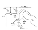
マトリックス素子をアドレス指定するために薄膜トランジスタ(TFT)の配列を使用することが公知である。例えば、指紋検出を行なうための1つの方法では、夫々のコンデンサの1つの極板として作用する電極のマトリックスが配置される。例えば図1を参照のこと。配列に近接して配置される指の隆起部及び谷部は、夫々のコンデンサの第2の極板として作用する。配列に含まれるコンデンサのキャパシタンス値は、配列の近傍に置かれる指の指紋の電子画像へ変換されうる。
【0003】
電子画像は、公知の順序で、配列をxy走査し、キャパシタンス値を検出することによって形成されうる。キャパシタンス値はコンデンサ上の電荷を測定することによって間接的に決定される。配列は順次に2回走査される。第1の走査中、各コンデンサはTFTによってアドレス指定され、既知の値Vpへ予め充電される。夫々のコンデンサに与えられる電荷はCiVpであり、但しCiは夫々の配列コンデンサのキャパシタンスである。第2の走査中、夫々の配列コンデンサは放電される。即ち、出力電圧値を与えるために電荷は除去され、また、蓄積される。検出された電圧値はキャパシタンス値に直接関係付けられる。
【0004】
ここで、例えば走査されるコンデンサ配列を形成するために、シリコン以外の基板上にTFTを形成する方法について考察する。この方法は、通常の集積回路処理ほど正確ではない。不正確さは製造される回路に望ましくない特徴を与えうる。例えば、TFTが、まず下層の基板上にゲート電極を堆積し、次にゲート電極上にTFTの本体部を形成することによって形成される場合、結果として得られるトランジスタは、通常は大きすぎて望ましくないゲート・ソース及びゲート・ドレインの重複キャパシタンスを有する。第2に、結果として得られるデバイスは、通常は大きすぎて望ましくない電圧を有し、より大きな活性化電圧等を必要とする。
【0005】
ここで、上記の特徴がいかにしてコンデンサ配列指紋検出器の動作に影響を与えうるかについて考察する。コンデンサ配列指紋検出器のダイナミックレンジは、検出されうるキャパシタンスの最大値対最小値の比率、又はより正確には、検出されうる対応する最大電荷対最少電荷の比率によって与えられる。最大キャパシタンスは隆起部の近傍の電極に関連づけられ、Qmaxの電荷に対応し、最少キャパシタンスはQminの電荷に対応すると仮定する。従って、予想ダイナミックレンジはQmax/Qminである。配列中の最少キャパシタンス値は指のいずれの部分の近傍にもない電極と関連づけられる。その値は漂遊キャパシタンスによってのみ決定され、非常に小さく、一定の値を有することが予想される。
【0006】
【発明が解決しようとする課題】
経済的な理由により、配列上のTFTは非晶質シリコン技術で形成されうる。これらのトランジスタの動作特徴は、これらのトランジスタのゲートに比較的大きな走査パルスが印加されることを必要とする。大きなゲートパルス電圧は、少なくとも部分的に、夫々のソース電極及びドレイン電極に印加される。このように、特定のTFTがゲートオフされる場合、いくらかの電荷は関連づけられる配列コンデンサから切り離される。次の走査中、TFTが感知動作のためにゲートオンされると、等しい量の電荷が配列コンデンサへ戻るよう印加されるであろう。本願の発明者は、この仮定が正しくないことを見いだし、それにより本発明に至った。
【0007】
【課題を解決するための手段】
比較的大きいキャパシタンス値を有する配列コンデンサは、TFTのゲート・ドレイン又はゲート・ソースの重複キャパシタンスよりもかなり大きいキャパシタンスを有する。従って、ゲートのターンオフ中に印加される全ての電荷は、電極(コンデンサ)の電圧を大きくは変更させない。この場合、予想されるように、トランジスタは、オフゲート電位が印加されるときにターンオフされる。
【0008】
比較的小さいキャパシタンス値を有する配列コンデンサは、TFTのゲート・ドレイン又はゲート・ソースの重複キャパシタンス値と同じオーダの又はわずかに大きいキャパシタンス値を有しうる。この場合、配列コンデンサ電極にかなりのターンオフゲート電圧が印加されうる。ゲート・コンデンサ電圧は、TFTのターンオン値(即ち閾値)を越え、それによりTFTがすぐにターンオフされコンデンサ電極を切り離すことを防止しうる。コンデンサはTFTをターンオフする点まで徐々に充電される。この充電の結果、コンデンサ上に指紋と関連づけられるキャパシタンスには関係のない追加的な電荷ΔQが生ずる。これは感知システムのダイナミックレンジを減少させる効果を有する。予想されるシステムダイナミックレンジQmax/Qminは、実際にはQmax/(Qmin+ΔQ)である。
【0009】
本願の発明者は、ターンオフパルス遷移の後に生ずるコンデンサの充電は、見かけのダイナミックレンジを高めるために有利に使用されうることを認識した。上述のダイナミックレンジ比では、電荷Qmin及びΔQが反対の極性であれば、電荷ΔQはQmin電荷のうちのいくらかを打ち消し、分母がゼロに近づき、見かけのダイナミックレンジを増加させる。
【0010】
【発明の実施の形態】
本発明は添付の図面を参照してより明らかとなろう。本発明は、容量性配列指紋検出器の環境で説明されるが、より広範な用途がある。典型的には、本発明は比較的大きな走査パルスが使用され、走査するTFTがいくらかのキャパシタンスを含む高インピーダンス素子に結合される任意の走査される配列において有用である。
【0011】
図1を参照するに、走査されるコンデンサ配列の一部が図示される。この例では、コンデンサ配列は各コンデンサの1つの極板のみを含む。アレイは、xy走査、素子走査、又はアドレス指定のための構成とされ、これらの走査は各コンデンサ極板に接続されるTFTによって実行される。行の全てのTFTのゲート電極又は制御電極は、共通行ゲート駆動電極に結合され、列の全てのTFTのドレイン電極は共通バスに接続される。回路(図示せず)の周囲付近において、行デコーダ及び列デコーダは順次に夫々の行バス及び列バスをストローブ又はアドレス指定する。一般的に、この種類の配列では、パルスは行の全てのTFTをオンとするために行バスのうちの1つにゲート駆動として印加され、列バスは信号検出回路によって順次に走査される。
【0012】
図2は配列の1つのセルをより詳細に示す図である。図2中、TFTに関連づけられる内在的且つ寄生的な容量性素子が含まれる。TFTのゲート及びドレイン電極間にはコンデンサCgdが存在し、ゲート及びソース電極間にはコンデンサCgsが存在する。概して、これらのコンデンサのキャパシタンス値は技術的に可能な限り最小とされる。通常の集積回路製造では、これらのコンデンサの値は自己整列ゲート技術により非常に小さい。残念ながら、自己整列ゲート製造技術は或るタイプのTFTの製造には使用可能でなく、結果として生ずるCgs及びCgdキャパシタンス値は比較的大きいものでありうる。
【0013】
検出器コンデンサは、実線で示される配列極板と、ファントムで示される第2の極板とを有する。第2の極板は、例えば人間の指又はその一部によってグランド電位に接続されると想定される。指の一部の近傍にない検出器コンデンサについては、そのキャパシタンスはゼロ値であると想定される。
【0014】
或る量の寄生容量は、コンデンサSTRAYによって示されるように検出器コンデンサの極板と内在的に関連づけられる。従って検出器キャパシタンスの最小値は寄生又は漂遊キャパシタンスとゲート・ソースキャパシタンスCgsとの並列な組合せに等しく、即ち指コンデンサは重要ではない。
【0015】
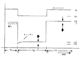
50ミクロン×50ミクロンのセンサピッチを有する配列(約35×35μmコンデンサ極板)を想定すると、最大指キャパシタンスは約40fF、全漂遊キャパシタンスは約6.8fFであると計算される。4μmのチャネル幅を有するスイッチングトランジスタでは、ゲート・ソースキャパシタンスは2fFのオーダである。これらのキャパシタンス値では、指キャパシタンスがない場合、選択トランジスタのゲートに印加されるパルス電圧の約3分の1が、コンデンサCgsによって配列指コンデンサ極板に結合される。例えば、15ボルトのゲートパルスを選択トランジスタに印加し、配列指極板を正の3ボルトに予め充電する場合について考慮する。選択トランジスタがターンオフされると、約5ボルトの負の電圧が指極板に結合され、負の2ボルトのプリチャージ値を生じさせる。通常、キャパシタンス電荷値を読み出すために選択されたトランジスタが正のパルスを与えられるとき、失われているプリチャージ電圧は回復されるため、かかる結合の影響は小さい。しかしながら、負の結合の大きさが、結果として生ずる選択トランジスタゲート・ソース電圧が閾値又はトランジスタのターンオン電圧よりも大きくなるような大きさである場合、トランジスタは予想されるようにターンオフされない。結果として、配列指極板の連続した充電又は放電が生じ、それにより誤って検出されたコンデンサ値を生じさせる。列電位が正の3ボルトのプリチャージ電位に維持されれば、指極板コンデンサは、選択トランジスタのゲート・ソース電位がその閾値以下になるまで正の方向に充電される。この充電効果の例は図3に示される(図示される電圧の縮尺は正しくない)。
【0016】
図3中、間隔TI1において、選択トランジスタはパルスがオンとされ、配列指極板コンデンサは3ボルトに予め充電される。時間T1において、選択トランジスタは15から0ボルトのゲートパルスを形成するよう負の方向の遷移によってスイッチオフされる。遷移の結果として、配列極板に4.5ボルトの負の電圧が結合される。トランジスタゲート電圧がここでゼロボルトであるため、正の1.5ゲート・ソース電圧がある。間隔TI2中の1ボルトのトランジスタ閾値を想定すると、トランジスタは正の導通性を維持する。配列極板キャパシタンスは、コンデンサ電圧が負の1ボルトに達し、トランジスタが導通を止める点まで負に充電される。
【0017】
時間T2において、配列コンデンサ上の電荷を読み出すため、選択トランジスタのゲートに正のパルスが印加される。ターンオンパルスの正の遷移は、4.5ボルトの正の電圧を配列コンデンサに印加し、その電位をマイナス1ボルトに4.5ボルトを足したもの、即ち正の3.5ボルトに上昇させる。これはプリチャージ値よりも0.5ボルト大きいか、或いは0.5ボルトの誤差がある。これは0.5×Cstrayの検出電荷誤りへ変換され、これは最小キャパシタンス値を実際の値よりも大きく見えさせ、それによりシステムのダイナミックレンジを減少させる。ゲートパルスが除去されたときに選択トランジスタが正しくターンオフするために、配列コンデンサ上の最小電荷はVpCstrayに等しく、但しVpはプリチャージ電圧である。ゲートパルスの負の遷移を配列コンデンサに印加することにより、最小電荷は実際には(Vp+ΔV)Cstrayとなり、但しΔVは間隔TI2に亘ってコンデンサの過剰な充電によって生じた誤り電圧である。
【0018】
システムのダイナミックレンジは比率Qmax/Qminによって与えられ、これはVpCmax/(Vp+ΔV)Cstray=Cmax/(1+ΔV/Vp)Cstrayに対応する。本願の発明者は、ΔV/Vpの項が負であれば、分母は小さくなり、有効ダイナミックレンジは高められることを認識した。これは、正ではなく負のプリチャージ電圧へ予め充電し、ゲートパルスの電圧レベルを適当に変化させることによって達成されうる。例えば、プリチャージ電圧を負の3ボルトに変更することは、システム駆動パラメータが等しいままであるためには負の6ボルトから正の9ボルトへのゲートパルス電圧レベルの変化を必要とする。ターンオフ遷移はやはり負の4.5ボルトを配列コンデンサ上に印加し、結果としてのゲート・ソース電圧は正の1.5ボルトとなり、トランジスタがターンオフされることを防止する。コンデンサは、ゲート・ソース電圧が負の7ボルトに達するまで正の0.5ボルトを充電し、その時点でトランジスタはターンオフされる。有効ダイナミックレンジはここで、Cmax/(1−ΔV/Vp)Csである。
【0019】
(1−ΔV/Vp)の項の値は、寄生パラメータ及び印加される電圧の関数である。寄生パラメータは、製造工程における予想できない変化により正確な評価を導かないことがある。これらのパラメータの変動を吸収するため、電圧値の幾つかは所望の(1−ΔV/Vp)値を発生するよう調整されうる。プリチャージ値Vpは、(1−ΔV/Vp)の値を制御するために調整されうる1つの変数である。しかしながら、信号対雑音比の考慮事項は、このパラメータが減少される量を決定する。QmaxはVpCmaxに等しいため、信号のサイズはVpに正比例する。Cmaxは数十fFのオーダであり、良い信号対雑音比を達成するためにはVpはできる限り大きくなくてはならない。
【0020】
調整を受ける他の変数はゲートパルス振幅である。この値は、多少のΔVを配列コンデンサ極板に印加させるよう調整されうる。この電圧に対するただ1つの制約は絶縁破壊制約である。第3に、配列コンデンサ極板への適切な結合を確実とするため、ゲート・ソース重複コンデンサは製造中に意図的に増加されうる。
【0021】
図4は、列バスのうちの1つに結合された感知増幅器を含むTFT走査されるコンデンサ配列の一部を示す図である。望ましくは各列は別個の感知増幅器に結合されるが、列はより少ない数の感知増幅器へと多重化されうる。
【0022】
図4中、列バスはスイッチS1によって可変電圧源Prechargeに選択的に結合され、電荷感知増幅器に選択的に結合される。電荷感知増幅器は、帰還コンデンサCintegrateに接続される演算増幅器即ちオペアンプである。スイッチS3は帰還コンデンサにまたがって接続され、所与の配列コンデンサ上の電荷を感知する前にコンデンサをリセットする。オペアンプは、公知のように電荷の蓄積をするように動作するときに、略ゼロの入力インピーダンスを表わす高利得装置である。従って、列バスに関連づけられるいずれのキャパシタンスも関連性がなく、検出機能の感度に影響を与えない。
【0023】
予め充電している間、スイッチS1は閉成され、スイッチS2は開成される。予め充電している間、選択トランジスタは一行毎にターンオンされるか、又は同時にターンオンされる。プリチャージサイクル中、配列全体は順次に走査され、次に読み出しのために配列全体が順次に走査される。或いは、コンデンサの夫々の行がまず予め充電され、次に感知される。
【0024】
信号読出し中、スイッチS1は開成され、スイッチS2は閉成される。通常、スイッチ値S2及びS3は交互に動作し、即ち、スイッチS2が閉成しているときスイッチS3は開成し、その逆に、スイッチS2が開成しているときスイッチS3は閉成する。スイッチS3は、夫々の電荷パケットの検出の間に蓄積コンデンサをリセットするために閉成される。スイッチS3は、走査TFTが導通しているとき、即ち感知間隔中はいつでも開成している。
【0025】
スイッチS2は、プリチャージ及び感知のいずれのモードにおいても夫々の行を感知する間に開成及び閉成するようにされている。或いは、S2は配列全体を順次に走査している間に閉成したままとされうる。
【0026】
行選択電極に結合されるゲート駆動は、可変直流源42と可変振幅パルス発生器40の直接接続を含む。装置は、夫々の機能を示す別個の回路素子として図示されるが、単一の総合的なパルス供給として配置されても良い。これらは、パルスの振れ及びその絶対振幅値は、レンジ制御の潜在的な源であることを示すよう図示されている。例えば、システムのダイナミックレンジは、プリチャージ電圧Vpを変更することによって調整される場合、パルス電圧の振れを変化させずにゲートパルスの直流レベルを調整することが必要である。過剰なコンデンサ電荷の量がゲート・ソース電圧の関数であるため、パルスの最も負の値はゲート・ソース電位式に入る。従って、VPが過剰なコンデンサ充電量に影響を与えるのと同様に、ゲート駆動パルスの最も負の直流値又はオフ電圧を変更させる。或いは、ΔVの値を調整するために、ダイナミックレンジがパルス振幅を変更させるために変更されねばならない場合、可変振幅パルス発生器が必要である。検出された信号のダイナミックレンジは、ゲート駆動パルス振幅、ゲート駆動パルスの最も負の値、及びプリチャージ電圧の値によって制御されうる。
【0027】
信号処理の分野の当業者によれば、キャパシタンスセンサから生成される表示された画像のコントラストは、同様の上述の変数によって調整されうることが認識されよう。
【0028】
例示的なキャパシタンス感知配列といったマトリクスを走査するために使用されるトランジスタの走査のタイプとは関係なく、夫々の配列コンデンサ極板に関連づけられる漂遊キャパシタンスがある。過剰なコンデンサ充電なしにターンオフされるトランジスタを走査するため、本発明によって教示されるように漂遊キャパシタンス上に蓄積される電荷を打ち消すためにかかる過剰な充電を実際に誘導することが有利である。これは単純に、走査パルスに通常必要とされる振幅を超過すること、又はより大きなトランジスタ重複キャパシタンス、例えばCgsを設計すること、そして漂遊キャパシタンス上に存在する電荷を打ち消すためにシステムを適切にバイアスすることによって達成されうる。
【0029】
請求の範囲において、遷移に関して「極性」という用語が用いられるときは、遷移が相対的に負の値から相対的に正の値に振れるときは正であり、相対的に正の値から相対的に負の値に振れるときは負であるものとする。
【図面の簡単な説明】
【図1】従来技術の走査されるコンデンサ配列を示す部分概略図である。
【図2】図1の配列の1つのセルをより詳細に示す概略図である。
【図3】TFTゲートパルスターンオフ遷移の発生の直前及び直後の配列コンデンサに伴う電圧を示す波形図である。
【図4】本発明を実施するTFT走査される配列を示す概略図である。
【符号の説明】
40 可変振幅パルス発生器
42 可変直流源
S1乃至S3 スイッチ[0001]
BACKGROUND OF THE INVENTION
The present invention relates to a method of operating a thin film transistor array, and more particularly to a method of operating a thin film transistor used to scan a capacitive matrix array.
[0002]
[Prior art]
It is known to use thin film transistor (TFT) arrays to address matrix elements. For example, in one method for performing fingerprint detection, a matrix of electrodes is placed that acts as one plate of each capacitor. See, for example, FIG. The ridges and troughs of the fingers placed in close proximity to the array act as second plates for the respective capacitors. Capacitance values of capacitors included in the array can be converted into an electronic image of a fingerprint of a finger placed in the vicinity of the array.
[0003]
An electronic image can be formed by xy scanning the array and detecting capacitance values in a known order. The capacitance value is indirectly determined by measuring the charge on the capacitor. The array is scanned twice in sequence. During the first scan, each capacitor is addressed by the TFT and precharged to a known value V p . The charge applied to each capacitor is C i V p , where C i is the capacitance of each array capacitor. During the second scan, each array capacitor is discharged. That is, the charge is removed and stored to provide an output voltage value. The detected voltage value is directly related to the capacitance value.
[0004]
Here, for example, a method of forming TFTs on a substrate other than silicon in order to form a scanned capacitor array will be considered. This method is not as accurate as normal integrated circuit processing. Inaccuracies can give undesirable characteristics to the manufactured circuit. For example, if a TFT is formed by first depositing a gate electrode on the underlying substrate and then forming the TFT body on the gate electrode, the resulting transistor is usually too large and desirable Has no gate-source and gate-drain overlap capacitance. Second, the resulting device is usually too large and has an undesirable voltage, requiring a larger activation voltage, etc.
[0005]
Now consider how the above features can affect the operation of the capacitor array fingerprint detector. The dynamic range of a capacitor array fingerprint detector is given by the ratio of the maximum to minimum capacitance that can be detected, or more precisely, the ratio of the corresponding maximum to minimum charge that can be detected. Assume that the maximum capacitance is associated with the electrode near the ridge and corresponds to a charge of Qmax and the minimum capacitance corresponds to a charge of Qmin. Therefore, the expected dynamic range is Qmax / Qmin. The minimum capacitance value in the array is associated with an electrode that is not near any part of the finger. Its value is determined only by stray capacitance and is expected to be very small and constant.
[0006]
[Problems to be solved by the invention]
For economic reasons, the TFTs on the array can be formed with amorphous silicon technology. The operational characteristics of these transistors require that a relatively large scan pulse be applied to the gates of these transistors. A large gate pulse voltage is applied at least partially to the respective source and drain electrodes. Thus, when a particular TFT is gated off, some charge is decoupled from the associated array capacitor. During the next scan, when the TFT is gated on for sensing operation, an equal amount of charge will be applied back to the array capacitor. The inventor of the present application has found that this assumption is not correct, thereby leading to the present invention.
[0007]
[Means for Solving the Problems]
An array capacitor having a relatively large capacitance value has a capacitance that is significantly greater than the overlapping capacitance of the gate-drain or gate-source of the TFT. Thus, all charges applied during gate turn-off do not significantly change the voltage on the electrode (capacitor). In this case, as expected, the transistor is turned off when an off-gate potential is applied.
[0008]
An array capacitor having a relatively small capacitance value may have a capacitance value on the same order as or slightly larger than the overlapping capacitance value of the gate-drain or gate-source of the TFT. In this case, a significant turn-off gate voltage can be applied to the array capacitor electrode. The gate capacitor voltage may exceed the TFT turn-on value (ie, threshold), thereby preventing the TFT from turning off immediately and disconnecting the capacitor electrode. The capacitor is gradually charged to the point where the TFT is turned off. This charging results in an additional charge ΔQ on the capacitor that is independent of the capacitance associated with the fingerprint. This has the effect of reducing the dynamic range of the sensing system. The expected system dynamic range Qmax / Qmin is actually Qmax / (Qmin + ΔQ).
[0009]
The inventors of the present application have recognized that capacitor charging that occurs after a turn-off pulse transition can be advantageously used to increase the apparent dynamic range. With the above dynamic range ratio, if the charges Qmin and ΔQ are of opposite polarity, the charge ΔQ cancels some of the Qmin charge and the denominator approaches zero, increasing the apparent dynamic range.
[0010]
DETAILED DESCRIPTION OF THE INVENTION
The invention will become more apparent with reference to the accompanying drawings. Although the present invention will be described in the context of a capacitive array fingerprint detector, it has a wider range of applications. Typically, the present invention is useful in any scanned array where relatively large scan pulses are used and the scanning TFT is coupled to a high impedance device that includes some capacitance.
[0011]
Referring to FIG. 1, a portion of a capacitor array that is scanned is illustrated. In this example, the capacitor array includes only one plate of each capacitor. The array is configured for xy scanning, device scanning, or addressing, and these scanning are performed by TFTs connected to each capacitor plate. The gate electrodes or control electrodes of all TFTs in a row are coupled to a common row gate drive electrode, and the drain electrodes of all TFTs in a column are connected to a common bus. Near the periphery of the circuit (not shown), the row and column decoders sequentially strobe or address their respective row and column buses. In general, in this type of arrangement, a pulse is applied as a gate drive to one of the row buses to turn on all the TFTs in the row, and the column bus is sequentially scanned by the signal detection circuit.
[0012]
FIG. 2 shows in more detail one cell of the array. In FIG. 2, intrinsic and parasitic capacitive elements associated with the TFT are included. A capacitor Cgd exists between the gate and drain electrodes of the TFT, and a capacitor Cgs exists between the gate and source electrodes. In general, the capacitance values of these capacitors are minimized as technically possible. In normal integrated circuit manufacturing, the value of these capacitors is very small due to the self-aligned gate technology. Unfortunately, self-aligned gate fabrication techniques cannot be used to fabricate certain types of TFTs and the resulting Cgs and Cgd capacitance values can be relatively large.
[0013]
The detector capacitor has an array plate indicated by a solid line and a second plate indicated by a phantom. The second electrode plate is assumed to be connected to the ground potential by, for example, a human finger or a part thereof. For detector capacitors that are not near the part of the finger, the capacitance is assumed to be zero.
[0014]
A certain amount of parasitic capacitance is inherently associated with the detector capacitor plate, as indicated by capacitor STRAY. The minimum value of the detector capacitance is therefore equal to the parallel combination of parasitic or stray capacitance and gate-source capacitance Cgs, i.e. the finger capacitor is not critical.
[0015]
Assuming an array with a sensor pitch of 50 microns × 50 microns (about 35 × 35 μm capacitor plate), the maximum finger capacitance is calculated to be about 40 fF and the total stray capacitance is about 6.8 fF. For a switching transistor having a channel width of 4 μm, the gate-source capacitance is on the order of 2 fF. At these capacitance values, in the absence of finger capacitance, approximately one third of the pulse voltage applied to the gate of the select transistor is coupled to the array finger capacitor plate by capacitor Cgs. For example, consider the case where a 15 volt gate pulse is applied to the select transistor and the array finger plate is precharged to positive 3 volts. When the select transistor is turned off, a negative voltage of approximately 5 volts is coupled to the finger plate, resulting in a negative precharge value of 2 volts. Usually, when the transistor selected to read the capacitance charge value is given a positive pulse, the lost precharge voltage is restored, so the effect of such coupling is small. However, if the magnitude of the negative coupling is such that the resulting select transistor gate-source voltage is greater than the threshold or transistor turn-on voltage, the transistor is not turned off as expected. As a result, a continuous charge or discharge of the array finger plate occurs, thereby producing a falsely detected capacitor value. If the column potential is maintained at a positive 3 volt precharge potential, the finger plate capacitor is charged in the positive direction until the gate-source potential of the select transistor is below its threshold. An example of this charging effect is shown in FIG. 3 (the voltage scale shown is not correct).
[0016]
In FIG. 3, at interval TI1, the select transistor is pulsed on and the array finger plate capacitor is precharged to 3 volts. At time T1, the select transistor is switched off by a negative transition to form a 15 to 0 volt gate pulse. As a result of the transition, a negative voltage of 4.5 volts is coupled to the array plate. Since the transistor gate voltage is now zero volts, there is a positive 1.5 gate-source voltage. Assuming a transistor threshold of 1 volt during interval TI2, the transistor remains positively conductive. The array plate capacitance is negatively charged until the capacitor voltage reaches a negative 1 volt and the transistor stops conducting.
[0017]
At time T2, a positive pulse is applied to the gate of the select transistor to read out the charge on the array capacitor. The positive transition of the turn-on pulse applies a positive voltage of 4.5 volts to the array capacitor and raises its potential to minus 1 volt plus 4.5 volts, ie positive 3.5 volts. This is 0.5 volts greater than the precharge value, or there is an error of 0.5 volts. This translates to a detected charge error of 0.5 × Cstray, which makes the minimum capacitance value appear larger than the actual value, thereby reducing the dynamic range of the system. In order for the select transistor to turn off correctly when the gate pulse is removed, the minimum charge on the array capacitor is equal to V p Cs, where V p is the precharge voltage. By applying a negative transition of the gate pulse to the array capacitor, the minimum charge is actually (V p + ΔV) Csray, where ΔV is the error voltage caused by excessive charging of the capacitor over the interval TI2.
[0018]
Dynamic range of the system is given by the ratio Qmax / Qmin, which corresponds to V p Cmax / (V p + ΔV) Cstray = Cmax / (1 + ΔV / V p) Cstray. The inventor of the present application has recognized that if the ΔV / V p term is negative, the denominator is reduced and the effective dynamic range is increased. This can be achieved by precharging to a negative precharge voltage rather than positive and appropriately changing the voltage level of the gate pulse. For example, changing the precharge voltage to negative 3 volts requires a change in the gate pulse voltage level from negative 6 volts to positive 9 volts in order for the system drive parameters to remain equal. The turn-off transition also applies a negative 4.5 volts on the array capacitor, resulting in a positive gate-source voltage of 1.5 volts, preventing the transistor from being turned off. The capacitor charges positive 0.5 volts until the gate-source voltage reaches negative 7 volts, at which point the transistor is turned off. Effective dynamic range here is a Cmax / (1-ΔV / V p) Cs.
[0019]
The value of the term (1-ΔV / V p ) is a function of the parasitic parameters and the applied voltage. Parasitic parameters may not lead to an accurate assessment due to unforeseen changes in the manufacturing process. In order to absorb variations in these parameters, some of the voltage values can be adjusted to produce the desired (1-ΔV / V p ) value. The precharge value V p is one variable that can be adjusted to control the value of (1−ΔV / V p ). However, signal to noise ratio considerations determine the amount by which this parameter is reduced. Since Qmax is equal to V p Cmax, the signal size is directly proportional to V p . Cmax is on the order of several tens of fF, and V p must be as large as possible to achieve a good signal-to-noise ratio.
[0020]
Another variable that is adjusted is the gate pulse amplitude. This value can be adjusted to apply some ΔV to the array capacitor plate. The only constraint on this voltage is a breakdown constraint. Third, the gate-source overlap capacitor can be intentionally increased during manufacture to ensure proper coupling to the array capacitor plate.
[0021]
FIG. 4 is a diagram illustrating a portion of a TFT-scanned capacitor array that includes a sense amplifier coupled to one of the column buses. Preferably each column is coupled to a separate sense amplifier, but the columns can be multiplexed into a smaller number of sense amplifiers.
[0022]
In FIG. 4, the column bus is selectively coupled to the variable voltage source Precharge by the switch S1 and is selectively coupled to the charge sense amplifier. The charge sense amplifier is an operational amplifier or operational amplifier connected to the feedback capacitor C integrate . Switch S3 is connected across the feedback capacitor and resets the capacitor before sensing the charge on a given array capacitor. An operational amplifier is a high gain device that exhibits a substantially zero input impedance when it operates to store charge as is well known. Thus, any capacitance associated with the column bus is irrelevant and does not affect the sensitivity of the detection function.
[0023]
During precharging, the switch S1 is closed and the switch S2 is opened. During precharging, the select transistors are turned on line by line or simultaneously. During the precharge cycle, the entire array is scanned sequentially and then the entire array is sequentially scanned for reading. Alternatively, each row of capacitors is first precharged and then sensed.
[0024]
During signal readout, switch S1 is opened and switch S2 is closed. Normally, the switch values S2 and S3 operate alternately, that is, the switch S3 is opened when the switch S2 is closed, and conversely, the switch S3 is closed when the switch S2 is opened. Switch S3 is closed to reset the storage capacitor during detection of each charge packet. Switch S3 is open whenever the scanning TFT is conducting, i.e. during the sensing interval.
[0025]
Switch S2 is configured to open and close while sensing each row in both precharge and sense modes. Alternatively, S2 can remain closed while sequentially scanning the entire array.
[0026]
The gate drive coupled to the row select electrode includes a direct connection between the
[0027]
Those skilled in the art of signal processing will recognize that the contrast of the displayed image generated from the capacitance sensor can be adjusted by the similar variables described above.
[0028]
Regardless of the type of transistor scanning used to scan the matrix, such as the exemplary capacitance sensing array, there is a stray capacitance associated with each array capacitor plate. In order to scan a transistor that is turned off without excessive capacitor charging, it is advantageous to actually induce such excessive charging to counteract the charge stored on the stray capacitance as taught by the present invention. This simply exceeds the amplitude normally required for a scan pulse, or designs a larger transistor overlap capacitance, eg Cgs, and properly biases the system to counteract the charge present on the stray capacitance. Can be achieved.
[0029]
In the claims, when the term “polarity” is used with respect to a transition, it is positive when the transition swings from a relatively negative value to a relatively positive value, and relative to a relatively positive value. Is negative when the value swings to a negative value.
[Brief description of the drawings]
FIG. 1 is a partial schematic diagram showing a prior art scanned capacitor array.
2 is a schematic diagram showing one cell of the array of FIG. 1 in more detail.
FIG. 3 is a waveform diagram showing a voltage associated with an array capacitor immediately before and immediately after the occurrence of a TFT gate pulse turn-off transition.
FIG. 4 is a schematic diagram illustrating a TFT scanned array embodying the present invention.
[Explanation of symbols]
40 variable
Claims (7)
前記薄膜トランジスタ装置が列バスと上記コンデンサとの間で導通することを調整するために前記薄膜トランジスタ装置に付随するゲートに走査パルスを与える段階であり、前記走査パルスは前記コンデンサが予め充電された後に前記薄膜トランジスタ装置を導通状態でなくさせる負の極性のターンオフ遷移を有する段階と、
前記遷移と同じ負の極性を有する直流プリチャージ電圧を前記列バスに供給する段階と、
を有することを特徴とする方法。A method of scanning a matrix of capacitors sequentially precharged to a precharge voltage by a matrix of associated thin film transistor devices connected to each capacitor,
Applying a scan pulse to a gate associated with the thin film transistor device to regulate conduction of the thin film transistor device between a column bus and the capacitor, the scan pulse after the capacitor is precharged Having a negative polarity turn-off transition that causes the thin film transistor device to become non-conductive;
Supplying a DC precharge voltage to the column bus having the same negative polarity as the transition;
A method characterized by comprising:
当該方法は、夫々のマトリックスコンデンサ上の電荷を感知するよう動作し、
当該方法は、感知された電荷のダイナミックレンジを調整するために前記走査パルスの振幅を可変に調整する段階を更に含む、
ことを特徴とする請求項1記載の方法。The array is a capacitance sensor array;
The method operates to sense the charge on each matrix capacitor;
The method further includes variably adjusting the amplitude of the scan pulse to adjust the dynamic range of the sensed charge.
The method of claim 1 wherein:
当該方法は、感知された電荷のダイナミックレンジを調整するために前記プリチャージ電圧の直流値を可変に調整する段階を更に含む、
ことを特徴とする請求項1記載の方法。The array is a capacitance sensor array that operates by sensing the charge on each matrix capacitor;
The method further includes variably adjusting the DC value of the precharge voltage to adjust the dynamic range of the sensed charge.
The method of claim 1 wherein:
当該方法は、感知された電荷のダイナミックレンジを調整するために前記走査パルスの直流振幅を可変に調整する段階を更に含む、
ことを特徴とする請求項3記載の方法。The array is a capacitance sensor array that operates by sensing the charge on each matrix capacitor;
The method further includes the step of variably adjusting the DC amplitude of the scan pulse to adjust the dynamic range of the sensed charge.
The method of claim 3 wherein:
当該方法は、夫々のマトリックスコンデンサ上の電荷を感知するよう動作し、
当該方法は、前記走査パルスの直流レベル及び前記走査パルスの振幅のうちの1つを調整することによって、感知されたコンデンサ値を表わす画像信号の彩度を調整する段階を更に含む、
ことを特徴とする請求項1記載の方法。The array is a capacitance sensor array;
The method operates to sense the charge on each matrix capacitor;
The method further includes adjusting the saturation of the image signal representing the sensed capacitor value by adjusting one of the DC level of the scan pulse and the amplitude of the scan pulse.
The method of claim 1 wherein:
列バスと夫々の前記キャパシタンスとの間に接続される夫々の薄膜トランジスタの導通路を有する走査薄膜トランジスタのマトリックスと、
前記薄膜トランジスタが導通することを調整するために夫々の前記薄膜トランジスタに走査パルスを与えるタイミング及びパルス発生器であり、前記走査パルスは前記薄膜トランジスタを導通状態でなくさせる負の極性の遷移を有する発生器と、
前記遷移と同じ負の極性を有するプリチャージ電圧源と、
電荷センサと、
前記プリチャージ電圧源又は前記電荷センサを前記列バスに選択的に接続するためのスイッチと、
を有することを特徴とする装置。A matrix of variable capacitance;
A matrix of scanning thin film transistors having respective thin film transistor conduction paths connected between a column bus and the respective capacitances;
A timing and pulse generator for applying a scan pulse to each of the thin film transistors to adjust the thin film transistor to be conductive, the scan pulse having a negative polarity transition that causes the thin film transistor to become non-conductive; and ,
A precharge voltage source having the same negative polarity as the transition;
A charge sensor;
A switch for selectively connecting the precharge voltage source or the charge sensor to the column bus;
A device characterized by comprising:
Applications Claiming Priority (2)
| Application Number | Priority Date | Filing Date | Title |
|---|---|---|---|
| US37692599A | 1999-08-18 | 1999-08-18 | |
| US376925 | 1999-08-18 |
Publications (3)
| Publication Number | Publication Date |
|---|---|
| JP2001076130A JP2001076130A (en) | 2001-03-23 |
| JP2001076130A5 JP2001076130A5 (en) | 2007-09-27 |
| JP4531219B2 true JP4531219B2 (en) | 2010-08-25 |
Family
ID=23487062
Family Applications (1)
| Application Number | Title | Priority Date | Filing Date |
|---|---|---|---|
| JP2000247363A Expired - Fee Related JP4531219B2 (en) | 1999-08-18 | 2000-08-17 | Method of operating capacitive thin film transistor array |
Country Status (4)
| Country | Link |
|---|---|
| JP (1) | JP4531219B2 (en) |
| KR (1) | KR100767648B1 (en) |
| CN (1) | CN1182484C (en) |
| TW (1) | TW501069B (en) |
Families Citing this family (5)
| Publication number | Priority date | Publication date | Assignee | Title |
|---|---|---|---|---|
| KR100473383B1 (en) * | 2002-07-19 | 2005-03-10 | 매그나칩 반도체 유한회사 | Unit fixel for capacitive fingerprint sensor and fingerprint sensing device having the same |
| KR100943271B1 (en) * | 2003-05-06 | 2010-02-23 | 삼성전자주식회사 | Apparatus for processing fingerprinting signal |
| JP3741282B2 (en) * | 2003-07-28 | 2006-02-01 | セイコーエプソン株式会社 | INPUT DEVICE, ELECTRONIC DEVICE, AND DRIVE METHOD FOR INPUT DEVICE |
| CN104408441A (en) * | 2014-12-10 | 2015-03-11 | 杨鹏飞 | Fingerprint identification sensor based on TFT film transistors and measurement method |
| CN105989350B (en) * | 2015-03-05 | 2019-11-22 | 上海箩箕技术有限公司 | Pixel unit, structure, array of structures, reading circuit and control method |
Citations (4)
| Publication number | Priority date | Publication date | Assignee | Title |
|---|---|---|---|---|
| JPH05215625A (en) * | 1991-10-15 | 1993-08-24 | Xerox Corp | Capacitive tactile sensor array |
| JPH05506347A (en) * | 1991-02-14 | 1993-09-16 | トムソン ソシエテ アノニム | Demultiplexer and 3-state gate used in it |
| JPH11508806A (en) * | 1996-04-26 | 1999-08-03 | フィリップス エレクトロニクス ネムローゼ フェンノートシャップ | Fingerprint detection device and system incorporating the same |
| JP2000514227A (en) * | 1997-04-29 | 2000-10-24 | コーニンクレッカ フィリップス エレクトロニクス エヌ ヴィ | Fingerprint sensing device and system incorporating the same |
Family Cites Families (2)
| Publication number | Priority date | Publication date | Assignee | Title |
|---|---|---|---|---|
| JP3110980B2 (en) * | 1995-07-18 | 2000-11-20 | インターナショナル・ビジネス・マシーンズ・コーポレ−ション | Driving device and method for liquid crystal display device |
| US5973658A (en) * | 1996-12-10 | 1999-10-26 | Lg Electronics, Inc. | Liquid crystal display panel having a static electricity prevention circuit and a method of operating the same |
-
2000
- 2000-08-08 TW TW089115927A patent/TW501069B/en not_active IP Right Cessation
- 2000-08-16 CN CNB001226878A patent/CN1182484C/en not_active Expired - Fee Related
- 2000-08-17 KR KR1020000047443A patent/KR100767648B1/en active IP Right Grant
- 2000-08-17 JP JP2000247363A patent/JP4531219B2/en not_active Expired - Fee Related
Patent Citations (4)
| Publication number | Priority date | Publication date | Assignee | Title |
|---|---|---|---|---|
| JPH05506347A (en) * | 1991-02-14 | 1993-09-16 | トムソン ソシエテ アノニム | Demultiplexer and 3-state gate used in it |
| JPH05215625A (en) * | 1991-10-15 | 1993-08-24 | Xerox Corp | Capacitive tactile sensor array |
| JPH11508806A (en) * | 1996-04-26 | 1999-08-03 | フィリップス エレクトロニクス ネムローゼ フェンノートシャップ | Fingerprint detection device and system incorporating the same |
| JP2000514227A (en) * | 1997-04-29 | 2000-10-24 | コーニンクレッカ フィリップス エレクトロニクス エヌ ヴィ | Fingerprint sensing device and system incorporating the same |
Also Published As
| Publication number | Publication date |
|---|---|
| CN1285568A (en) | 2001-02-28 |
| TW501069B (en) | 2002-09-01 |
| JP2001076130A (en) | 2001-03-23 |
| KR20010050098A (en) | 2001-06-15 |
| KR100767648B1 (en) | 2007-10-17 |
| CN1182484C (en) | 2004-12-29 |
Similar Documents
| Publication | Publication Date | Title |
|---|---|---|
| US6556935B2 (en) | Small shape recognizing capacitive sensor device | |
| EP0980563B1 (en) | Fingerprint sensing device, with capacitive matrix and system incorporating such device | |
| US6556646B1 (en) | Shift register | |
| US5289401A (en) | Analog storage device for artificial neural network system | |
| KR100968401B1 (en) | Driving apparatus for display | |
| KR100463859B1 (en) | Physical quantity distribution detecting semiconductor device and driving method thereof | |
| JP3701924B2 (en) | EL array substrate inspection method and inspection apparatus | |
| JPS62164300A (en) | Electrically erasable/programmable semiconductor memory cell | |
| WO2003006925A1 (en) | Electrostatic capacitance sensor and fingerprint collator comprising it | |
| JPH08263028A (en) | Shift register | |
| EP0329141B1 (en) | Sense circuit incorporated in semiconductor memory device | |
| JP3044660B1 (en) | Sensor circuit for surface shape recognition | |
| JP3289126B2 (en) | Video display | |
| JP4531219B2 (en) | Method of operating capacitive thin film transistor array | |
| US7474570B2 (en) | Semiconductor device | |
| KR100400048B1 (en) | Ferroelectric memory device | |
| JP3696176B2 (en) | Imaging device | |
| JPH0412675B2 (en) | ||
| JP3606233B2 (en) | Semiconductor integrated circuit, semiconductor device having a large number of semiconductor integrated circuits, and electronic equipment using the semiconductor device | |
| US7372719B2 (en) | DRAM semiconductor memory device with increased reading accuracy | |
| US11227137B2 (en) | Sensor pixel and fingerprint sensing sensor including the same | |
| JP3270927B2 (en) | Sensor circuit for surface shape recognition | |
| JP3425945B2 (en) | Surface shape recognition sensor device | |
| US20240232599A9 (en) | Neural network circuit with delay line | |
| JP2813838B2 (en) | Analog memory device and control circuit |
Legal Events
| Date | Code | Title | Description |
|---|---|---|---|
| A521 | Request for written amendment filed |
Free format text: JAPANESE INTERMEDIATE CODE: A523 Effective date: 20070814 |
|
| A621 | Written request for application examination |
Free format text: JAPANESE INTERMEDIATE CODE: A621 Effective date: 20070814 |
|
| A131 | Notification of reasons for refusal |
Free format text: JAPANESE INTERMEDIATE CODE: A131 Effective date: 20091124 |
|
| A521 | Request for written amendment filed |
Free format text: JAPANESE INTERMEDIATE CODE: A523 Effective date: 20100217 |
|
| TRDD | Decision of grant or rejection written | ||
| A01 | Written decision to grant a patent or to grant a registration (utility model) |
Free format text: JAPANESE INTERMEDIATE CODE: A01 Effective date: 20100511 |
|
| A01 | Written decision to grant a patent or to grant a registration (utility model) |
Free format text: JAPANESE INTERMEDIATE CODE: A01 |
|
| A61 | First payment of annual fees (during grant procedure) |
Free format text: JAPANESE INTERMEDIATE CODE: A61 Effective date: 20100609 |
|
| R150 | Certificate of patent or registration of utility model |
Ref document number: 4531219 Country of ref document: JP Free format text: JAPANESE INTERMEDIATE CODE: R150 Free format text: JAPANESE INTERMEDIATE CODE: R150 |
|
| FPAY | Renewal fee payment (event date is renewal date of database) |
Free format text: PAYMENT UNTIL: 20130618 Year of fee payment: 3 |
|
| R250 | Receipt of annual fees |
Free format text: JAPANESE INTERMEDIATE CODE: R250 |
|
| LAPS | Cancellation because of no payment of annual fees |