JP4524082B2 - Flexible imager and CT scanner with flexible imager - Google Patents
Flexible imager and CT scanner with flexible imager Download PDFInfo
- Publication number
- JP4524082B2 JP4524082B2 JP2003278693A JP2003278693A JP4524082B2 JP 4524082 B2 JP4524082 B2 JP 4524082B2 JP 2003278693 A JP2003278693 A JP 2003278693A JP 2003278693 A JP2003278693 A JP 2003278693A JP 4524082 B2 JP4524082 B2 JP 4524082B2
- Authority
- JP
- Japan
- Prior art keywords
- imager
- substrate
- flexible
- array
- disposed
- Prior art date
- Legal status (The legal status is an assumption and is not a legal conclusion. Google has not performed a legal analysis and makes no representation as to the accuracy of the status listed.)
- Expired - Lifetime
Links
- 239000000758 substrate Substances 0.000 claims description 58
- 230000005855 radiation Effects 0.000 claims description 53
- 239000004065 semiconductor Substances 0.000 claims description 28
- 238000003384 imaging method Methods 0.000 claims description 27
- 238000010438 heat treatment Methods 0.000 claims description 20
- 238000002591 computed tomography Methods 0.000 claims description 17
- 229910021417 amorphous silicon Inorganic materials 0.000 claims description 16
- 239000010409 thin film Substances 0.000 claims description 11
- XQPRBTXUXXVTKB-UHFFFAOYSA-M caesium iodide Chemical compound [I-].[Cs+] XQPRBTXUXXVTKB-UHFFFAOYSA-M 0.000 claims description 8
- 230000003287 optical effect Effects 0.000 claims description 8
- OAICVXFJPJFONN-UHFFFAOYSA-N Phosphorus Chemical compound [P] OAICVXFJPJFONN-UHFFFAOYSA-N 0.000 claims description 6
- 239000004642 Polyimide Substances 0.000 claims description 5
- 229920001721 polyimide Polymers 0.000 claims description 5
- 230000008859 change Effects 0.000 claims description 4
- 229920000620 organic polymer Polymers 0.000 claims description 4
- 229920005570 flexible polymer Polymers 0.000 claims 1
- 238000000034 method Methods 0.000 description 29
- 239000010410 layer Substances 0.000 description 28
- 238000007689 inspection Methods 0.000 description 20
- 238000012545 processing Methods 0.000 description 16
- 239000010408 film Substances 0.000 description 13
- 239000000463 material Substances 0.000 description 13
- 239000010931 gold Substances 0.000 description 12
- PXHVJJICTQNCMI-UHFFFAOYSA-N Nickel Chemical compound [Ni] PXHVJJICTQNCMI-UHFFFAOYSA-N 0.000 description 10
- 230000008901 benefit Effects 0.000 description 10
- KDLHZDBZIXYQEI-UHFFFAOYSA-N Palladium Chemical compound [Pd] KDLHZDBZIXYQEI-UHFFFAOYSA-N 0.000 description 9
- 239000011651 chromium Substances 0.000 description 9
- 238000004519 manufacturing process Methods 0.000 description 9
- 238000009413 insulation Methods 0.000 description 8
- 229910052737 gold Inorganic materials 0.000 description 7
- 229910004298 SiO 2 Inorganic materials 0.000 description 6
- PCHJSUWPFVWCPO-UHFFFAOYSA-N gold Chemical compound [Au] PCHJSUWPFVWCPO-UHFFFAOYSA-N 0.000 description 6
- 239000000976 ink Substances 0.000 description 6
- 229910052750 molybdenum Inorganic materials 0.000 description 6
- BASFCYQUMIYNBI-UHFFFAOYSA-N platinum Chemical compound [Pt] BASFCYQUMIYNBI-UHFFFAOYSA-N 0.000 description 6
- 229910052782 aluminium Inorganic materials 0.000 description 5
- 230000015572 biosynthetic process Effects 0.000 description 5
- VYZAMTAEIAYCRO-UHFFFAOYSA-N Chromium Chemical compound [Cr] VYZAMTAEIAYCRO-UHFFFAOYSA-N 0.000 description 4
- ZOKXTWBITQBERF-UHFFFAOYSA-N Molybdenum Chemical compound [Mo] ZOKXTWBITQBERF-UHFFFAOYSA-N 0.000 description 4
- VYPSYNLAJGMNEJ-UHFFFAOYSA-N Silicium dioxide Chemical compound O=[Si]=O VYPSYNLAJGMNEJ-UHFFFAOYSA-N 0.000 description 4
- XAGFODPZIPBFFR-UHFFFAOYSA-N aluminium Chemical compound [Al] XAGFODPZIPBFFR-UHFFFAOYSA-N 0.000 description 4
- 229910052804 chromium Inorganic materials 0.000 description 4
- 239000011733 molybdenum Substances 0.000 description 4
- 229910052759 nickel Inorganic materials 0.000 description 4
- -1 polyethylene terephthalate Polymers 0.000 description 4
- 229920000642 polymer Polymers 0.000 description 4
- XLOMVQKBTHCTTD-UHFFFAOYSA-N Zinc monoxide Chemical compound [Zn]=O XLOMVQKBTHCTTD-UHFFFAOYSA-N 0.000 description 3
- 238000004458 analytical method Methods 0.000 description 3
- 238000005266 casting Methods 0.000 description 3
- 229920001940 conductive polymer Polymers 0.000 description 3
- 230000007797 corrosion Effects 0.000 description 3
- 238000005260 corrosion Methods 0.000 description 3
- 238000001514 detection method Methods 0.000 description 3
- 239000011521 glass Substances 0.000 description 3
- 229910052763 palladium Inorganic materials 0.000 description 3
- 238000000206 photolithography Methods 0.000 description 3
- 229910052697 platinum Inorganic materials 0.000 description 3
- 239000010936 titanium Substances 0.000 description 3
- 229920001609 Poly(3,4-ethylenedioxythiophene) Polymers 0.000 description 2
- 239000004697 Polyetherimide Substances 0.000 description 2
- 239000004698 Polyethylene Substances 0.000 description 2
- 229910052581 Si3N4 Inorganic materials 0.000 description 2
- 229920001646 UPILEX Polymers 0.000 description 2
- UMIVXZPTRXBADB-UHFFFAOYSA-N benzocyclobutene Chemical compound C1=CC=C2CCC2=C1 UMIVXZPTRXBADB-UHFFFAOYSA-N 0.000 description 2
- 230000015556 catabolic process Effects 0.000 description 2
- 239000004020 conductor Substances 0.000 description 2
- 230000007547 defect Effects 0.000 description 2
- 238000006731 degradation reaction Methods 0.000 description 2
- 230000001066 destructive effect Effects 0.000 description 2
- 238000011161 development Methods 0.000 description 2
- 230000018109 developmental process Effects 0.000 description 2
- 239000003989 dielectric material Substances 0.000 description 2
- 238000005516 engineering process Methods 0.000 description 2
- RBTKNAXYKSUFRK-UHFFFAOYSA-N heliogen blue Chemical compound [Cu].[N-]1C2=C(C=CC=C3)C3=C1N=C([N-]1)C3=CC=CC=C3C1=NC([N-]1)=C(C=CC=C3)C3=C1N=C([N-]1)C3=CC=CC=C3C1=N2 RBTKNAXYKSUFRK-UHFFFAOYSA-N 0.000 description 2
- AMGQUBHHOARCQH-UHFFFAOYSA-N indium;oxotin Chemical compound [In].[Sn]=O AMGQUBHHOARCQH-UHFFFAOYSA-N 0.000 description 2
- 238000012986 modification Methods 0.000 description 2
- 230000004048 modification Effects 0.000 description 2
- SLIUAWYAILUBJU-UHFFFAOYSA-N pentacene Chemical compound C1=CC=CC2=CC3=CC4=CC5=CC=CC=C5C=C4C=C3C=C21 SLIUAWYAILUBJU-UHFFFAOYSA-N 0.000 description 2
- 238000007747 plating Methods 0.000 description 2
- 229920000052 poly(p-xylylene) Polymers 0.000 description 2
- 229910021420 polycrystalline silicon Inorganic materials 0.000 description 2
- 229920001601 polyetherimide Polymers 0.000 description 2
- 229920000573 polyethylene Polymers 0.000 description 2
- 229920000139 polyethylene terephthalate Polymers 0.000 description 2
- 239000005020 polyethylene terephthalate Substances 0.000 description 2
- 238000007639 printing Methods 0.000 description 2
- 230000008569 process Effects 0.000 description 2
- 230000004044 response Effects 0.000 description 2
- 235000012239 silicon dioxide Nutrition 0.000 description 2
- 239000000377 silicon dioxide Substances 0.000 description 2
- HQVNEWCFYHHQES-UHFFFAOYSA-N silicon nitride Chemical compound N12[Si]34N5[Si]62N3[Si]51N64 HQVNEWCFYHHQES-UHFFFAOYSA-N 0.000 description 2
- IFLREYGFSNHWGE-UHFFFAOYSA-N tetracene Chemical compound C1=CC=CC2=CC3=CC4=CC=CC=C4C=C3C=C21 IFLREYGFSNHWGE-UHFFFAOYSA-N 0.000 description 2
- 125000001544 thienyl group Chemical group 0.000 description 2
- 229910052721 tungsten Inorganic materials 0.000 description 2
- 229910018072 Al 2 O 3 Inorganic materials 0.000 description 1
- 239000004593 Epoxy Substances 0.000 description 1
- 229920012266 Poly(ether sulfone) PES Polymers 0.000 description 1
- 239000004952 Polyamide Substances 0.000 description 1
- BUGBHKTXTAQXES-UHFFFAOYSA-N Selenium Chemical compound [Se] BUGBHKTXTAQXES-UHFFFAOYSA-N 0.000 description 1
- XUIMIQQOPSSXEZ-UHFFFAOYSA-N Silicon Chemical compound [Si] XUIMIQQOPSSXEZ-UHFFFAOYSA-N 0.000 description 1
- GWEVSGVZZGPLCZ-UHFFFAOYSA-N Titan oxide Chemical compound O=[Ti]=O GWEVSGVZZGPLCZ-UHFFFAOYSA-N 0.000 description 1
- RTAQQCXQSZGOHL-UHFFFAOYSA-N Titanium Chemical compound [Ti] RTAQQCXQSZGOHL-UHFFFAOYSA-N 0.000 description 1
- MCVAAHQLXUXWLC-UHFFFAOYSA-N [O-2].[O-2].[S-2].[Gd+3].[Gd+3] Chemical compound [O-2].[O-2].[S-2].[Gd+3].[Gd+3] MCVAAHQLXUXWLC-UHFFFAOYSA-N 0.000 description 1
- 230000003213 activating effect Effects 0.000 description 1
- 239000000853 adhesive Substances 0.000 description 1
- 230000001070 adhesive effect Effects 0.000 description 1
- 238000013459 approach Methods 0.000 description 1
- 238000003491 array Methods 0.000 description 1
- 230000004888 barrier function Effects 0.000 description 1
- 238000005452 bending Methods 0.000 description 1
- 239000011230 binding agent Substances 0.000 description 1
- 239000011195 cermet Substances 0.000 description 1
- 239000011247 coating layer Substances 0.000 description 1
- 238000002247 constant time method Methods 0.000 description 1
- 238000010276 construction Methods 0.000 description 1
- 238000001816 cooling Methods 0.000 description 1
- 239000010949 copper Substances 0.000 description 1
- 230000008878 coupling Effects 0.000 description 1
- 238000010168 coupling process Methods 0.000 description 1
- 238000005859 coupling reaction Methods 0.000 description 1
- 230000007423 decrease Effects 0.000 description 1
- 230000000593 degrading effect Effects 0.000 description 1
- 238000000151 deposition Methods 0.000 description 1
- 230000008021 deposition Effects 0.000 description 1
- JAONJTDQXUSBGG-UHFFFAOYSA-N dialuminum;dizinc;oxygen(2-) Chemical compound [O-2].[O-2].[O-2].[O-2].[O-2].[Al+3].[Al+3].[Zn+2].[Zn+2] JAONJTDQXUSBGG-UHFFFAOYSA-N 0.000 description 1
- 238000010017 direct printing Methods 0.000 description 1
- 238000009826 distribution Methods 0.000 description 1
- 230000000694 effects Effects 0.000 description 1
- 238000010894 electron beam technology Methods 0.000 description 1
- 230000001747 exhibiting effect Effects 0.000 description 1
- 239000000835 fiber Substances 0.000 description 1
- 230000005669 field effect Effects 0.000 description 1
- 239000012530 fluid Substances 0.000 description 1
- 238000011010 flushing procedure Methods 0.000 description 1
- 239000004519 grease Substances 0.000 description 1
- 238000007641 inkjet printing Methods 0.000 description 1
- 238000010884 ion-beam technique Methods 0.000 description 1
- 230000001678 irradiating effect Effects 0.000 description 1
- 238000012423 maintenance Methods 0.000 description 1
- 238000013507 mapping Methods 0.000 description 1
- 230000007246 mechanism Effects 0.000 description 1
- 229910052751 metal Inorganic materials 0.000 description 1
- 239000002184 metal Substances 0.000 description 1
- 239000007769 metal material Substances 0.000 description 1
- 229910044991 metal oxide Inorganic materials 0.000 description 1
- 150000004706 metal oxides Chemical class 0.000 description 1
- 238000012544 monitoring process Methods 0.000 description 1
- 239000002105 nanoparticle Substances 0.000 description 1
- 238000010943 off-gassing Methods 0.000 description 1
- 230000005693 optoelectronics Effects 0.000 description 1
- 150000007530 organic bases Chemical class 0.000 description 1
- TWNQGVIAIRXVLR-UHFFFAOYSA-N oxo(oxoalumanyloxy)alumane Chemical compound O=[Al]O[Al]=O TWNQGVIAIRXVLR-UHFFFAOYSA-N 0.000 description 1
- 239000002245 particle Substances 0.000 description 1
- 229920002647 polyamide Polymers 0.000 description 1
- 229920000728 polyester Polymers 0.000 description 1
- 239000011112 polyethylene naphthalate Substances 0.000 description 1
- 230000002265 prevention Effects 0.000 description 1
- 230000009467 reduction Effects 0.000 description 1
- 230000007261 regionalization Effects 0.000 description 1
- 238000007650 screen-printing Methods 0.000 description 1
- 238000007789 sealing Methods 0.000 description 1
- 239000011669 selenium Substances 0.000 description 1
- 229910052711 selenium Inorganic materials 0.000 description 1
- 230000035945 sensitivity Effects 0.000 description 1
- 229910052710 silicon Inorganic materials 0.000 description 1
- 239000010703 silicon Substances 0.000 description 1
- 239000002904 solvent Substances 0.000 description 1
- 238000003860 storage Methods 0.000 description 1
- MZLGASXMSKOWSE-UHFFFAOYSA-N tantalum nitride Chemical compound [Ta]#N MZLGASXMSKOWSE-UHFFFAOYSA-N 0.000 description 1
- 229910003451 terbium oxide Inorganic materials 0.000 description 1
- SCRZPWWVSXWCMC-UHFFFAOYSA-N terbium(iii) oxide Chemical compound [O-2].[O-2].[O-2].[Tb+3].[Tb+3] SCRZPWWVSXWCMC-UHFFFAOYSA-N 0.000 description 1
- 238000012360 testing method Methods 0.000 description 1
- 229910052716 thallium Inorganic materials 0.000 description 1
- BKVIYDNLLOSFOA-UHFFFAOYSA-N thallium Chemical compound [Tl] BKVIYDNLLOSFOA-UHFFFAOYSA-N 0.000 description 1
- 230000005676 thermoelectric effect Effects 0.000 description 1
- 229910052719 titanium Inorganic materials 0.000 description 1
- 238000012546 transfer Methods 0.000 description 1
- 238000002834 transmittance Methods 0.000 description 1
- WFKWXMTUELFFGS-UHFFFAOYSA-N tungsten Chemical compound [W] WFKWXMTUELFFGS-UHFFFAOYSA-N 0.000 description 1
- 239000010937 tungsten Substances 0.000 description 1
- 238000001771 vacuum deposition Methods 0.000 description 1
- 239000002699 waste material Substances 0.000 description 1
- 239000011787 zinc oxide Substances 0.000 description 1
Images


Classifications
-
- H—ELECTRICITY
- H01—ELECTRIC ELEMENTS
- H01L—SEMICONDUCTOR DEVICES NOT COVERED BY CLASS H10
- H01L27/00—Devices consisting of a plurality of semiconductor or other solid-state components formed in or on a common substrate
- H01L27/14—Devices consisting of a plurality of semiconductor or other solid-state components formed in or on a common substrate including semiconductor components sensitive to infrared radiation, light, electromagnetic radiation of shorter wavelength or corpuscular radiation and specially adapted either for the conversion of the energy of such radiation into electrical energy or for the control of electrical energy by such radiation
- H01L27/144—Devices controlled by radiation
- H01L27/146—Imager structures
- H01L27/14601—Structural or functional details thereof
-
- G—PHYSICS
- G01—MEASURING; TESTING
- G01T—MEASUREMENT OF NUCLEAR OR X-RADIATION
- G01T1/00—Measuring X-radiation, gamma radiation, corpuscular radiation, or cosmic radiation
- G01T1/16—Measuring radiation intensity
- G01T1/20—Measuring radiation intensity with scintillation detectors
- G01T1/2018—Scintillation-photodiode combinations
- G01T1/20185—Coupling means between the photodiode and the scintillator, e.g. optical couplings using adhesives with wavelength-shifting fibres
-
- G—PHYSICS
- G01—MEASURING; TESTING
- G01T—MEASUREMENT OF NUCLEAR OR X-RADIATION
- G01T1/00—Measuring X-radiation, gamma radiation, corpuscular radiation, or cosmic radiation
- G01T1/16—Measuring radiation intensity
- G01T1/20—Measuring radiation intensity with scintillation detectors
- G01T1/2018—Scintillation-photodiode combinations
- G01T1/20188—Auxiliary details, e.g. casings or cooling
Description
本発明は、一般的に放射線イメージャに関し、より具体的には、可撓性があり、適合性があってかつ堅牢な放射線イメージャに関する。 The present invention relates generally to radiographic imagers, and more particularly to a radiographic imager that is flexible, adaptable and robust.
放射線画像形成システムは、医療及び産業用途に幅広く用いられている。ソリッドステート式放射線イメージャを用いて得られた画像は、電気的に分析及び格納されることが有益である。しかしながら、従来のソリッドステート式放射線イメージャは、重く、壊れやすくかつ剛直であり、典型的にはガラス基板上に形成されている。これは、移動性、堅牢性及び軽量性が必要とされる産業上の適用を制限するものとなる。
従って、他の方法ではデジタル画像形成のためにアクセスできないような密閉区域においてイメージャを用いることを含む、産業上の適用を可能にするような、可撓性がありかつ堅牢性があるイメージャを提供することが望ましい。 Accordingly, a flexible and robust imager is provided that allows industrial applications, including using the imager in an enclosed area that would otherwise not be accessible for digital imaging. It is desirable to do.
手短に述べると、本発明の1つの実施形態によれば、入射する放射線によって照射された被写体を画像化するための可撓性イメージャが開示される。可撓性イメージャは、可撓性基板と、該可撓性基板上に配置された光センサ・アレイと、シンチレータとを含む。シンチレータは、入射する放射線を受けかつ吸収するように配置され、該入射する放射線を光子に変換するように構成され、かつ光センサ・アレイに光学的に結合されている。光センサ・アレイは、光子を受けて、該光子に対応する電気信号を生成するように構成される。 Briefly, according to one embodiment of the present invention, a flexible imager for imaging a subject illuminated by incident radiation is disclosed. The flexible imager includes a flexible substrate, a photosensor array disposed on the flexible substrate, and a scintillator. The scintillator is arranged to receive and absorb incident radiation, is configured to convert the incident radiation into photons, and is optically coupled to the photosensor array. The photosensor array is configured to receive photons and generate electrical signals corresponding to the photons.
被写体を画像化するためのデジタル画像形成方法の実施形態が更に開示される。デジタル画像形成方法は、可撓性デジタルイメージャを、被写体が該可撓性デジタルイメージャと放射線源との間に位置決めされるように該被写体に適合させるステップを含む。このデジタル画像形成方法は更に、放射線源を作動させて被写体を放射線に曝すステップと、可撓性デジタルイメージャを用いて画像を収集するステップとを含む。 Further disclosed is an embodiment of a digital image forming method for imaging a subject. The digital imaging method includes adapting a flexible digital imager to the subject such that the subject is positioned between the flexible digital imager and the radiation source. The digital imaging method further includes activating the radiation source to expose the subject to the radiation and collecting the image using a flexible digital imager.
本発明のこれら及び他の特徴、態様及び利点は、同じ符号が図面全体にわたって同じ部分を表している添付図面を参照して、以下の詳細な説明を読むことにより、一層よく理解されるであろう。 These and other features, aspects and advantages of the present invention will be better understood when the following detailed description is read with reference to the accompanying drawings in which like numerals represent like parts throughout the drawings, wherein: Let's go.
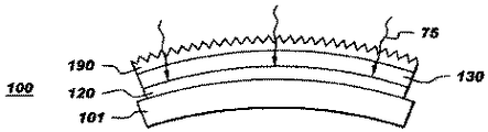
図1及び図8を参照しながら、入射する放射線75により照射された被写体200を画像化するための可撓性イメージャ100について説明する。図示するように、可撓性イメージャ100は、可撓性基板101と、可撓性基板101上に配置された光センサ・アレイ110とを含む。可撓性イメージャ100は更に、入射する放射線75を受けかつ吸収するように配置されたシンチレータ190を含む。シンチレータ190は、入射する放射線75を光子に変換するように構成され、かつ光センサ・アレイ110に光学的に結合されている。例示的な入射する放射線75は、典型的には、約0.0005オングストロームから約5オングストロームまでの間の範囲内の波長を有するX線を含む。光センサ・アレイ110は、光子を受けて、該光子に対応する電気信号を生成するように構成されている。可撓性イメージャ100の一般的な構造は、参考文献として本明細書に組み入れられる、「薄膜トランジスタのアドレス指定可能なアレイを有するソリッドステート式X線透視放射線イメージャ」と題する、本発明の出願人に譲渡されたJack D.Kingsleyらによる米国特許第5,587,591号と同様のものであることに注目されたい。しかしながら、このソリッドステート式X線透視放射線イメージャの公知の基板は剛直な(可撓性がない)ものであり、例えば、ガラスを含むものである。これとは対照的に、基板101は、図1及び図2に例示的な曲率によって示されるように可撓性がある。有利なことに、可撓性基板101は堅牢であり、ガラスのような剛直な基板上に作製されたイメージャが乱暴な取扱及び輸送状態によって損傷を受けがちな現場での使用を可能にする。その上、可撓性基板101により、ユーザが、例えば航空機構造体の一部などの被検査被写体200の表面に、可撓性イメージャ100を適合させることが可能になる。
A
光センサ・アレイ110により生成された電気信号に対応する画像を表示するために、読み取り及びリセット回路210が光センサ・アレイ110に電気的に接続されて、入射する放射線75に応答して生成された電気的信号を受信する。読み取り及びリセット回路210は更に、該読み取り及びリセット回路から伝送された信号を処理して、情報を可撓性イメージャ100のユーザに提供する表示及び分析装置220に接続される。
A read and
より具体的な実施形態によると、可撓性基板101はポリマーから形成される。より具体的には、可撓性基板101は、ポリイミドのようなフレキシブル有機ポリマーから形成され、こうしたポリマーの例には、Kapton(商標)及びUpilex(商標)の商標名で市販されている材料が含まれる。Upilex(商標)は、UBE Industries,Ltd.から市販されており、Kapton(商標)は、E.I.du Pont de Nemours and Companyから市販されている。他の例示的なフレキシブル有機ポリマーには、BASF製のポリエーテルスルホン(PES)と、E.I.du Pont de Nemours and Company製のポリエチレンテレフタレート(PET又はポリエステル)と、E.I.du Pont de Nemours and Company製のポリエチレンナフタレート(PEN)と、General Electric製のポリエーテルイミド(PEI)とが含まれる。
According to a more specific embodiment, the
加工処理中の機械的な安定性をもたらしながら可撓性イメージャ100の可撓性を高めるには、可撓性基板101は、特定の実施形態によると、約2ミル乃至約10ミルの厚さにされる。より特定的には、可撓性基板101は、約3ミル乃至約8ミルの厚さにされる。例示的な可撓性基板の厚さは約5ミルである(1ミルは千分の1インチ、1インチは、2.54cm)。
To increase the flexibility of the
例示的な光センサ・アレイ110の一部が図3に示される。図示するように、光センサ・アレイ110は、多数の光センサ120と、アドレス指定可能な薄膜トランジスタ(TFT)アレイ130とを含む。より具体的には、各光センサ120は、例えばアモルファス・ケイ素(a−Si)の光ダイオードといった光ダイオード120を含む。TFTアレイ130は多数のTFT134を含み、該TFTの各々は、光センサ・アレイ110において各光センサ120が選択的にアドレス指定されるように、光センサ120の1つとそれぞれ電気的に接続される。図3に示すように、例示的な光センサ・アレイ110は更に、光センサ120の各々を選択的にアドレス指定することができる走査ライン131とデータライン132とを含む。有利なことに、Iowa Thin Films Technology,Inc,から市販されているポリイミドのa−Siシートを加工して、可撓性基板上に配置された光ダイオードを形成することができる。
A portion of an
光センサ・アレイ110の一般的な構造は、本発明の出願人に譲渡された上述の米国特許第5,587,591号の図1(B)に示されているものと同じであることに注目されたい。従って、光センサ・アレイ110の詳細な説明を省略する。手短に述べると、例示的なTFT134は、例えば図4に示すように、ゲート電極138と、該ゲート電極138の上に配置された半導体領域139と、該半導体領域139に接触するソース電極137及びドレイン電極136とを含む。図5に示すTFT134の特定の積層構造においては、半導体領域139はゲート誘電層102の上に配置される。また、ソース電極137及びドレイン電極136を形成する際に用いられる典型的な材料及び技術に加えて、従来の写真平版技術を必要としない材料を用いることもできる。ソース電極137及びドレイン電極136の従来の材料には、金(Au)、パラジウム(Pd)、白金(Pt)、ニッケル(Ni)、クロム(Cr)、アルミニウム(Al)、モリブデン(Mo)、タングステン(W)、チタン(Ti)、及び酸化スズインジウム(ITO)が含まれる。しかしながら、ソース電極137及びドレイン電極136はまた、場合によっては低コストでインクジェット又はスクリーン印刷のような公知の技術を用いて、例えば、酸化チタン(TiO2)及び金(Au)のような金属性ナノ粒子を含む電気的に伝導性のある(「導電性の」)インクか、又はポリエチレンジオキシチオフェン(PEDOT)のような導電性ポリマーから形成することもできる。産業上の画像形成の用途では、関係する速度が僅かに低く及び/又は関係する電圧が僅かに高いので、導電性インク又は導電性ポリマーから形成されたソース電極137及びドレイン電極136が受け入れられる。より具体的な実施形態によると、ゲート電極138は、導電性インク又は導電性ポリマーから形成されて、例えば、約1乃至約10nmRMSの粗度をもつ、ほぼピンホールのない滑らかな表面を形成し、該表面上に優れた表面品質及び電気的性質を有するゲート誘電層102を形成可能にする。走査ライン131及びデータライン132は、Au、Ni、Al、Mo、及びクロム/金(Cr/Au)又はクロム/モリブデン(Cr/Mo)の二重層のような導電性材料から形成される。例示的な走査ライン131及びデータライン132が図2に示されている。
The general structure of the
特定の実施形態によると、TFT134は、例えば、上述の米国特許第5,587,591号に開示されている従来のアモルファス・ケイ素(a−Si)ベースのTFTである。手短に述べると、ソース電極137及びドレイン電極136は、図4に示すように、半導体領域の上に配置される。この実施形態において、半導体領域139は、例えば図5に示すように、真性a−Si層103と、該真性a−Si層の上に配置されたドープ処理a−Si層104とを含む。a−SiベースのTFT134は、キャリアの電界効果移動度、サブスレショルド勾配、及びソース/ドレイン電流のオン/オフ比について、望ましい素子特性をもたらす利点がある。より具体的には、アドレス指定可能なTFTアレイ130は、可撓性基板101と光センサ120との間に位置し、各光センサ120はa−Si光ダイオード120を備える。この実施形態において、例示的な走査ライン131は、アルミニウム(Al)から又はクロム/モリブデン(Cr/Mo)の二重層から形成され、例示的なデータライン132はモリブデン(Mo)を含む。更に、各TFT134は、図5に示すように、ゲート電極138と半導体領域139との間に配置されるゲート誘電層102を含む。従来のゲート誘電層102は、窒化ケイ素(SiNx)又は二酸化ケイ素(SiO2)から形成される。しかしながら、可撓性イメージャ100の可撓性を高めるために、ゲート誘電層102はまた、ポリイミド、ポリアミド、パリレン、ベンゾシクロブテン(BCB)、その他の同様な有機誘電物質などの有機誘電材料から形成することもできる。
According to certain embodiments, the
写真平版技術のような加工処理の際の機械的安定性をもたらすために、可撓性イメージャ100は更に、例えば図5に示すように、可撓性基板101とアドレス指定可能なTFTアレイ130との間に配置された被覆層105を含むことができる。例示的な被覆層105は、窒化ケイ素(SiNx)、二酸化ケイ素(SiO2)、及び酸化アルミニウム(Al2O3)を含む。被覆層105の他の利点は、防湿障壁をもたらして、写真平版技術のような加工処理中の溶剤のガス抜け及びポリマー鎖の分解を防ぐことを含む。
In order to provide mechanical stability during processing, such as photolithography, the
図1に示される特定の実施形態において、可撓性イメージャ100は更に、可撓性基板101の背面107上に配置された背面層106を含む。より具体的には、背面層106は加熱素子108を含み、例示的な背面層106は、Mo、W、Pt、多結晶シリコン(Poly−Si)、酸化亜鉛(ZnO)、窒化タンタル(TaNx)、導電性インク、又はCr/SiO2、Ta/SiO2、Ti/SiO2及びW/SiO2のような抵抗性サーメット材料から形成される。加熱素子108は、例えば、フィルムパターン形成のための平版印刷法に組み込まれた、上述の材料の真空蒸着、電極メッキ、又は無電極メッキによって作製される。別の例示的な背面層106の作製には、平版印刷法の代わりに導電性インクの直接印刷が用いられる。
In the particular embodiment shown in FIG. 1, the
特定の実施形態によると、加熱素子108は、デバイスの加工処理中に可撓性基板101内で局所的に熱を再分配し、また可撓性基板101を全体的に加熱及び冷却するための導電性の熱電極(図示せず)を含む。このように、背面層106が、デバイスの加工処理中における可撓性基板101の寸法安定性を高める。加熱素子108の働きは、電流を熱電極に印加して、熱電効果すなわちジュール熱効果を生み出すことを含む。熱電効果に基づく加熱素子108においては、熱電極に対する熱の移動方向は、印加された電流の極性に依存する。熱電極の特定の寸法及び幾何学的形状は、光センサ・アレイ110の寸法及び幾何学的形状、並びに特定の用途に関連する他の因子によって変化する。
According to certain embodiments, the
電流が加熱素子108を通って流れるときに、結果として生じる加熱素子108における温度勾配によって、熱電加熱すなわちジュール加熱の法則に基づいて光センサ・アレイ110の加工処理領域の対応する部分について定められた通りに可撓性基板101が局所的に収縮又は膨張するように、加熱素子108の抵抗率が選択される。可撓性基板101の背面107上に加熱素子108を設けることにより、背面層106が、加工処理中の可撓性基板101の熱寸法変化を動的に制御し、相殺する、という利点が得られる。1つの例示的な実施形態においては、背面層106は、可撓性基板101の加工処理中の収縮又は膨張を、約百万分の1から約百万分の1000(ppm)までの範囲内で補正する。
As current flows through the
別の例示的な製造に関する実施形態においては、デバイス加工処理中に、外付けの加熱装置(図示せず)を可撓性基板101上に取り付けて、可撓性基板101の熱寸法変化を動的に制御し、相殺する。外付けの加熱装置は、可撓性イメージャ100の製造後に可撓性基板101から容易に取り外すことができる。特筆すべきことは、背面層106と外付けの加熱装置との両方によって、デバイス加工処理中の可撓性基板101への加熱及び冷却制御機構の実装が容易になり、加工処理中の可撓性基板101の寸法安定性が能動的に制御され、維持されることである。
In another exemplary manufacturing embodiment, an external heating device (not shown) is mounted on the
有機半導体もまた、それらが機械的な可撓性があること、及び室温での蒸着処理が可能であることから、半導体領域に望ましい材料である。従って、別の実施形態においては、半導体領域139は、有機半導体(又は「有機半導体領域」)を含む。例示的な有機半導体には、ペンタセン、ナフタセン、銅フタロシアニン、及びアルファ−6チエニルが含まれる。この実施形態において、例示的な走査ライン131は、ニッケル(Ni)又はアルミニウム(Al)を含み、例示的なデータライン132はパラジウム(Pd)又は金(Au)を含む。より具体的には、有機半導体領域139は、ソース電極137及びドレイン電極136の上に配置される。後者の形態は、例えば金又は白金を含む通常のソース電極137及びドレイン電極136の写真平版印刷処理及び蒸着の際に、有機半導体領域139を保護する利点がある。ソース電極137及びドレイン電極136が導電性インク又は導電性ポリマーを用いて形成される場合には、有機半導体領域139の上部にソース電極137及びドレイン電極136を形成するのが、このような上部での電極形態が全体的に優れた性能となるため、有利である。ここで用いられる「〜の上に」という用語及び「〜の上部に」という語句は、可撓性基板101に対して定義されるものである。例えば、ソース電極137及びドレイン電極136が、有機半導体領域139「の上部に」(又は「の上に」)配置されるという意味は、ソース電極137及びドレイン電極136が、例えば図5に示すように、有機半導体領域139よりも可撓性基板101から更に遠くに配置されていることを示す。可撓性イメージャ100のこの有機半導体の実施形態においては、光センサ120は、光センサ120の形成に関係する加工処理から有機半導体領域139を更に保護するために、図6に示すように、可撓性基板101とアドレス指定可能なTFTアレイ130との間に位置させられることが望ましい。この実施形態の特定の態様によると、TFT134は、シンチレータ190により発生された光子がTFT134を通して光センサ120に伝わるように、光学的に透明にされる。光学的に透明なTFT134は、透明なソース電極136、ドレイン電極137及びゲート電極138と、ペンタセン、ナフタセン、銅フタロシアニン及びアルファ−6チエニルのような薄く透明な有機半導体139とを含む。例示的な透明なソース電極136、ドレイン電極137及びゲート電極138は、酸化インジウム・スズ(In2O3:Sn,ITO)及びアルミニウム酸化亜鉛(ZnO:Al,AZO)のような透明な導電性金属酸化物か、又はアルミニウム(Al)、パラジウム(Pd)、ニッケル(Ni)及び金(Au)のような高い光透過率及び電気伝導率を示す電子ビーム又はイオンビーム蒸着された超薄金属フィルムを含む。
Organic semiconductors are also desirable materials for semiconductor regions because they are mechanically flexible and can be deposited at room temperature. Thus, in another embodiment, the
従来のデジタルイメージャと同様に、シンチレータ190は、入射する放射線の大部分を吸収して光子を生成するように、入射する放射線75に対して比較的大きい断面をもつように選択される。シンチレータ190のための1つの例示的な材料は、例えばタリウムがドープされたヨウ化セシウムのようなヨウ化セシウム(CsI)である。有利なことに、ヨウ化セシウム(CsI)は、X線に対して比較的大きい断面をもつ。特定の実施形態によると、CsIのような特定の蛍光材料が薄膜として蒸着される。別の実施形態によると、CsIはファイバ形状で形成される。他の例示的なシンチレータ材料は、この業界では公知の技術を用いることにより、結着剤を用いて光センサ・アレイ110上に直接付着される。別の実施形態によると、シンチレータ190は、アモルファスセレンのような光電陰極材料を含む。この実施形態においては、光センサ・アレイ110は、光ではなく電子を検出するように構成される。別の実施形態については、シンチレータ190は蛍光体スクリーン190を含む。蛍光体スクリーン190は、例えば、光学エポキシ、UV硬化型接着剤又は光結合グリースを介して光センサ・アレイ110に光学的に結合される。例示的な蛍光体スクリーン190は、酸化テルビウムにより活性化されたガドリニウム酸硫化物を含む。他の例示的な蛍光体スクリーン190には、BaFCl:Eu2+、YTaO4及びZnCdS:CuのようなX線蛍光体が多結晶粒子状に形成され、最終的にX線の蛍光体スクリーン190に形成されたものが含まれる。
As with conventional digital imagers, the
シンチレータ190を保護するために、可撓性イメージャ100はまた、図1に示すように、シンチレータ190の上に配置されたカバー層195を含むことができる。例示的なカバー層195はパリレンから形成される。より具体的な実施形態によると、カバー層195はシンチレータ190に入射する周辺光を遮断するように構成され、1つの例示的な材料はポリエチレンを含み、該材料は、黒い可撓性の有機ベース材料であることが望ましい。例示的なカバー層195はポリエチレンのスリーブを含み、該スリーブはX線フィルムを覆うために用いられる場合が多く、シンチレータ190の遮光シールを形成するのに有利である。
To protect the
入射する放射線75によって照射された被写体200を画像化するための可撓性デジタルイメージャ100の実施形態を、図1、図3及び図7を参照して説明する。上述の特徴についての説明は繰り返さない。手短に述べると、図1に示すように、可撓性デジタルイメージャ100は、可撓性基板101と、可撓性基板101上に配置された光センサ・アレイ110と、シンチレータ190とを含む。上述のように、光センサ・アレイ110は、多数の光センサ120と、アドレス指定可能な薄膜トランジスタTFTアレイ130とを含む。図3及び図7に示すように、光センサ120は、多数の列211と、少なくとも1つの行212とを形成するように配列される。特定の実施形態によると、可撓性基板101はフレキシブル有機ポリマーから形成され、約3ミル乃至約8ミルの厚さにされる。より特定的な実施形態によると、可撓性デジタルイメージャ100は更に、上述のように、可撓性基板101の背面107上に配置された背面層106を含む。上述のように、例示的なTFT134は、a−Si又は有機半導体領域130を組み込まれる。
An embodiment of a flexible
図7に示す実施形態において、光センサ120は1つの行212を形成するように配列される。この形態の場合には、光センサ・アレイ110は線形配列を形成する。有利なことに、加工処理中の可撓性基板101の熱に起因する寸法変化は、加工処理面積の縮小に伴って減少するので、可撓性基板101上への線形配列構成の作製は、比較的容易である。
In the embodiment shown in FIG. 7, the
可撓性イメージャ100の線形配列の実施形態の特に有用な用途の1つは、医療又は産業上の画像形成のためのコンピュータ断層撮影(CT)システム(図示せず)の1次検出要素(即ち、同様に参照符号100で示される線形配列CTスキャナ)を供給することである。コンピュータ断層撮影の用途においては、線形配列CTスキャナ100は、典型的には、例えば図10に示すように、放射線の円錐状ビームの方向に傾斜させられる。現在、医療用の線形配列CTスキャナの製造は、光センサ(例えば、シリコンダイオード)及びシンチレータの個々のモジュールを、隣接する光センサ/シンチレータのモジュールが互いに僅かな角度をなして位置決めされて、入射するX線と位置合わせされるように製作し、組み立てられるという点でかなり労働集約的である。これとは対照的に、図10の例示的な線形配列CTスキャナ100においては、各光センサ120は、隣接する光センサ120に対して所定の角度をなして配向されて、入射する放射線75と位置合わせされる。1つの実施形態によると、可撓性基板110及び線形光センサ・アレイ110は、光センサ120の各々の位置及び相対的配向が一定になるような固定構成で配列される。別の実施形態においては、線形光センサ・アレイ110及び可撓性基板110は、光センサ120の各々を隣接する光センサの1つに対して所定の角度をなして配列されるように調節可能に構成される。後者の実施形態においては、可撓性イメージャ100には可撓性があるので、光センサ120の行212は、可撓性イメージャ100と放射線源300との間の距離の変化に対して調節されて、例えば検査中の被写体200の幾何学的倍率を変化させるように位置決めし直されるように構成される。有利なことに、線形配列CTスキャナ100の製造工程は、上述の線形配列CTスキャナの現在の製造工程に比べて単純である。更に、線形配列CTスキャナ100においては、光センサ120は、個別の光センサ・セルの配列ではなく、連続的な行212として構成され、より低いコストでX線ビーム75に対する優れた位置合わせをもたらす。
One particularly useful application of the linear array embodiment of the
図3に示される実施形態において、光センサ120は、多数の行212を成して、2次元(2D)光センサ・アレイ110を形成するように配列される。有利なことに、2Dアレイは、列211及び行212の数と、光センサ120の寸法に応じて、被写体200の大きな部分の画像化を可能にする。より具体的には、2Dアレイは、単一走査から2D画像を生成し、より幅広い面積を画像化する能力を与える。2Dアレイは更に、1回の走査で多数の被写体又は断続的な特徴をもつ被写体を画像化することができる。こうした能力は、例えば、航空機の胴体若しくはエンジンの一部、船体の一部、又はプリント回路基板及び光学電子チップのような部品の一部の画像化といった、産業上の非破壊検査の用途に望ましい。他の将来的に可能性のある用途には、例えば、宇宙ステーションで宇宙飛行士及び作業者の医学的診断を飛行中にリアルタイムで実行することや、宇宙での高エネルギー放射能源をマッピングすることのような宇宙開発が含まれる。更に、線形配列の実施形態に関して上述したのと同様の位置合わせ及び製造の利点が、同様に可撓性イメージャ100の2Dアレイの実施形態にも当てはまる。
In the embodiment shown in FIG. 3,
可撓性イメージャ100の2Dの実施形態は、製造検査及び実用現場検査の用途の両方に特に有用である。例えば、現在の大規模な構造用鋳造物(図示せず)のX線検査には、X線フィルム(図示せず)を緊密な組立体の中に滑り込ませること、及び、X線源により該構造用鋳造物の反対側の面を照射させながら、X線フィルムを構造用鋳造物に適合させることが必要である。有利なことに、可撓性イメージャ100は、リアルタイムで適合可能な検出器であり、いずれも高いアラインメント感度がいる亀裂又は熱間亀裂のような欠陥について、可撓性イメージャ100の配向に迅速なフィードバックを与える。従って、露光及び位置合わせが有効であるかどうかを確認する前に、一般的に10分以上が費やされるゆっくりとしたフィルム露光に対して、可撓性イメージャ100を用いると、これらの緊密な線形特徴の位置合わせ及び検出がより容易に可能となる。また、例えば、陸上用又は航空機用のガスタービンエンジンについての実用現場検査の用途にも、可撓性イメージャ100のこの2Dの実施形態により利点が生じる。可撓性イメージャ100は、狭い場所の中に置くことができ、かつ検査を受ける構造体に適合させることができる可撓性のリアルタイムのデバイスであることが利点である。このようにして、可撓性イメージャ100は、欠陥アラインメント位置の場所を求めるのに有用な特定の重要な場所に接近するために、及び高解像度の非破壊検査を実行する前に適切な露光条件を迅速に確認するために用いることができる。
The 2D embodiment of the
デジタル画像形成方法の実施形態を、図8を参照して説明する。このデジタル画像形成方法は、図8に示すように、可撓性デジタルイメージャ100を被写体200に適合させるステップを含む。可撓性デジタルイメージャ100は、シンチレータが被写体200と向い合うように位置決めされる。例えば、X線源などの放射線源300を作動させて、被写体200を放射線75に曝す。このようにして、X線75のような放射線75が、被写体200を通り抜けて、シンチレータ190に衝突する。この方法は更に、可撓性デジタルイメージャ100を用いて画像を収集するステップを含む。例えば、入射する放射線75に応答して可撓性デジタルイメージャ100により生成された電気信号が、読み取り及びリセット回路210によって受信され、該読み取り及びリセット回路210は更に、図1に関して上述し及び図8に示すように、表示及び分析装置220に接続されている。
An embodiment of a digital image forming method will be described with reference to FIG. This digital image forming method includes the step of adapting a flexible
図3及び図7に示すように、可撓性デジタルイメージャ100は、線形配列か又は2次元(2D)配列のいずれかで配列された多数の光センサ120を含むことができる。上述のように、線形配列構成は製造上の利点をもたらすのに対して、2D配列は2D画像形成及び幅広い画像形成能力をもたらす。線形配列は、画像形成する被写体200の1次元情報を与え、2D情報は画像走査の際に移動可能な線形配列構成を用いて取得されることができるが、これは2D配列構成を用いて単一走査を実行することに比べて、2D画像形成の複雑さ及びコストを増加させる。
As shown in FIGS. 3 and 7, the flexible
本発明の方法について考えられる適用例の1つは航空機の検査である。この適用例を図9に示すが、この場合、被写体200は、例えば民間航空機といった航空機の一部である。図9に示す配置において、被写体200は胴体200であり、胴体200の少なくとも一部の周り、より具体的には、胴体200の外板244の周りを可撓性イメージャ100で包む。図9に示すように、胴体200は、フレーム236と、多数のストリンガ234と、少なくとも1つのポート穴242とを含み、放射線源300はデッキ238上に位置決めされる。現在、民間航空機の検査は、胴体200の構造上重要なフレーム236及びストリンガ234を検査するために、側板及び断熱材232の取り外しを必要とする。しかしながら、本発明の方法は、断熱材232、オーバヘッドビン230及び側壁240を通してのストリンガ234及びフレーム236の検査を可能にし、これによって取り外ししなくても検査ができるようになり、このことにより検査コストが削減され、断熱材232の再組み立てに関連した潜在的な問題が回避される。可撓性デジタルイメージャ100は、例えば、Iowa Thin Films Technology,Inc,から市販されているようなポリイミドa−Siシートを用いて、大型シート状に形成するのが有利である。胴体200の周りを包むことができる可撓性デジタルイメージャ100のこの大規模な実施形態は、胴体検査のためにロール状にして輸送可能である。1つの例示的な放射線源300は、高圧電源装置(図示せず)によって電源供給されるパノラマ式X線管300である。パノラマ式X線管は、例えば、約60度を超える幅広い角度分布をもつ放射線を放射する。しかしながら、このデジタル画像形成方法は、特定の形式の放射線源300に限定されるものではない。このようにして、胴体300のような航空機構造体200を効率的に検査して、デジタル画像を形成し、多量のX線フィルムの使用及び処分を避けることができる。
One possible application for the method of the present invention is aircraft inspection. FIG. 9 shows an example of this application. In this case, the subject 200 is a part of an aircraft such as a civil aircraft. In the arrangement shown in FIG. 9, the subject 200 is a
他の望ましい適用例は、従来の剛直なデジタルX線パネルが破損しがちな凹凸の激しい領域にアクセス可能な遠隔位置で使用することを含む。本発明の方法の別の望ましい適用例は、剛直なX線パネルでは不可能な狭い開口部の中といったアクセスが難しい場所に可撓性イメージャ100を位置決めすること、即ち曲げることである。有利なことに、本発明の方法のこれらの適用例は、以前にはX線フィルム(図示せず)しか用いることができなかった場所及び位置でのデジタル画像形成を可能にし、コンピュータ(図示せず)を用いて容易に格納及び分析されるデジタル画像をもたらし、X線フィルムの使用、保存及び処分を避ける。その上、現場でのフィルムによるX線撮影式画像形成は、フィルム現像機(図示せず)を検査場所に持ち込むか、又は現像のためにフィルムを暗室に戻すかのいずれかを必要とする場合が多い。直ちに利用できるラップトップ・コンピュータ220と組み合わされた本発明のデジタル画像形成方法は、これらの手法のいずれの必要性も排除し、検査の即時理解をもたらす。更に、航空機の画像形成に加えて、他の望ましい適用例には、原子炉チャンバ、耐放射線性装置及び放射線防止構造体、並びに廃棄物処理のパイプライン及び機械類のような原子力施設における装置及び計測器、並びにパイプライン(図示せず)の腐食又は劣化している溶接部を検出するために、画像形成することが含まれる。
Another desirable application involves the use of a conventional rigid digital X-ray panel at a remote location that is accessible to an uneven area that is prone to breakage. Another desirable application of the method of the present invention is to position or bend the
本発明の方法についての他の例示的な適用例には、建設中及び/又は保守中の宇宙飛行の機器類、衛星及び宇宙ステーションの部品の画像形成が含まれる。これらの例示的な適用例の場合、可撓性イメージャ100は、部品、ストラット、壁及び支持構造体に焦点を合わせて適合される。
Other exemplary applications for the method of the present invention include imaging of space flight equipment, satellites and space station components under construction and / or maintenance. For these exemplary applications, the
別のデジタル画像形成方法の実施形態を、図10を参照して説明する。このデジタル画像形成方法は、放射線源300を用いて被写体200を画像形成するようにされており、該放射線源は、図10に示すように、拡がった放射線ビームを放射するように構成されている。このデジタル画像形成方法は、可撓性デジタルイメージャ100を曲げるステップを含み、そのため、シンチレータ190は、図10に示すように円柱状構造196をもち、該円柱状構造が拡がった放射線ビームと平行に位置合わせされる。可撓性デジタルイメージャ100は、被写体200が放射線源300と該可撓性デジタルイメージャ100との間にくるように位置決めされる。被写体200は、上述のように画像形成される。その上、このデジタル画像形成方法は更に、放射線源300と可撓性デジタルイメージャ100との間の距離dを調節するステップを含み、シンチレータ190の円柱状構造196を拡がった放射線ビーム75に更に位置合わせすることができる。この実施形態の有利な適用例は、コンピュータ断層撮影を含む。可撓性イメージャ100の線形配列CTスキャナの実施形態に関して上で説明したように、本発明の方法は、現在のCT方法に対して製造の容易さ及び低コストと優れた位置合わせとの両方の利点を有する。
Another embodiment of the digital image forming method will be described with reference to FIG. In this digital image forming method, a subject 200 is imaged using a
別のデジタル画像形成方法の実施形態を、図11及び図12を参照して説明する。このデジタル画像形成法は、被写体200の1つ又はそれ以上の部分を繰り返し画像形成するようにされており、少なくとも1つの可撓性デジタルイメージャ100を被写体200内に埋め込むステップと、放射線源300を作動させて被写体200を拡がった放射線ビーム75に曝すステップとを含む。被写体200の一部は、放射線源300と可撓性デジタルイメージャ100との間に位置決めされる。この方法は更に、可撓性デジタルイメージャ100を用いて画像を収集するステップを含む。ここで用いられる「被写体200を放射線75に曝す」という語句は、被写体200の少なくとも一部を放射線75に曝すことを意味すると理解されたい。被写体200の幾つかの部分を画像形成するために、多数の可撓性デジタルイメージャ100を被写体200内に埋め込むことができる。特定の実施形態においては、被写体200は航空機構造体の一部である。
Another embodiment of the digital image forming method will be described with reference to FIGS. The digital imaging method is configured to repeatedly image one or more portions of the subject 200, embedding at least one flexible
図11に示す特定の実施形態において、被写体200は胴体200であり、可撓性デジタルイメージャ100は、図示するように胴体200と断熱層232との間に埋め込まれる。より具体的には、図11に示す航空機検査の適用例の場合には、可撓性デジタルイメージャ100は、ストリンガ234及び重ね継手部246を画像形成するように位置合わせされる。図11の例示的な構造において、電源及びデータライン202は、オーバヘッドビン232を貫通して、より具体的には、ジャンクションボックス248の外に延びて、読み取り及びリセット回路210、表示及び分析装置220又は電源装置(図示せず)に接続される。或いは、可撓性デジタルイメージャ100は、このような外部装置に遠隔的に接続される。有利なことに、胴体200内の断熱材232の下にある重ね継手部246に沿って可撓性デジタルイメージャ100を位置決めすることにより、亀裂及び腐食の検出及び監視が、断熱材232を取り外し及び再取り付けすることなく、これらの構造的に重要な場所において繰り返し実行できる。
In the particular embodiment shown in FIG. 11, the subject 200 is a
別の航空機検査の適用例が図12に示されており、この場合、被写体200は翼200であり、可撓性デジタルイメージャ100は、翼200の一部を画像形成するために、翼200の内面204上に組み込まれる。航空機についての多数の検査は、典型的には、作業者が翼200に入って放射線用フィルム(図示せず)を設置し、要所となる翼の構造要素の完全性を確認することを必要とする。有利なことに、図12に示す航空機検査の適用例は、翼に入る回数を削減し、かつ可撓性デジタルイメージャ100が検査から次の検査まで同じ位置にあるので、これらの構造要素の安定した追跡をもたらす。
Another aircraft inspection application is shown in FIG. 12, where the subject 200 is a
他の例示的な構造体には、原子力施設におけるパイプライン部分と装置と計測器とが含まれる。図13はこれもまた参照符号200によって示されるパイプラインの一部へのデジタル画像形成方法の適用を断面図で示すものである。図13に示すように、この実施形態の場合、可撓性デジタルイメージャ100は、腐食及び亀裂のような異常270を検出・監視するために、断熱材232及びフラッシング260の下のパイプライン200内に組み込まれている。より具体的には、可撓性デジタルイメージャ100は、パイプラインの溶接部(図示せず)沿いといった、パイプライン200の内側で腐食が生じることが知られている重要な領域の付近に位置決めされる。可撓性デジタルイメージャ100を劣化から保護するために、可撓性デジタルイメージャは、従来のシーリング手段によりプロセス流体(図示せず)からシールされる。図13に示す特定の実施形態において、可撓性イメージャは可動PIGに接続され、電力を受け、画像形成データ(又は信号)を供給する。次に、この信号は可動PIG262により無線で送信される。
Other exemplary structures include pipeline sections, equipment and instruments in a nuclear facility. FIG. 13 shows, in cross-section, the application of the digital image forming method to a portion of the pipeline, also indicated by
ここでは本発明の特定の特徴のみを図示し、説明してきたが、当業者であれば多くの修正及び変更を想い付くであろう。従って、本明細書と同時に提出した特許請求の範囲は、そのような修正及び変更の全てを本発明の技術思想に含まれるものとして保護することを意図していることを理解されたい。 Although only certain features of the invention have been illustrated and described herein, many modifications and changes will occur to those skilled in the art. Accordingly, it is to be understood that the claims appended hereto are intended to protect all such modifications and changes as being included in the spirit of the invention.
75 入射する放射線
100 可撓性イメージャ
101 可撓性基板
106 背面層
108 加熱素子
110 光センサ・アレイ
190 シンチレータ
195 カバー層
75
Claims (10)
可撓性のポリマーを含む基板(101)と、
前記基板(101)の背面(107)上に配置された背面層(106)であって、複数の加熱素子(108)を備える前記背面層と、
前記基板上に配置された光センサ・アレイ(110)と、
前記入射する放射線を受けかつ吸収するように配置され、前記入射する放射線を光子に変換するように構成され、前記光センサ・アレイに光学的に結合されたシンチレータ(190)と、
を備え、
前記複数の加熱素子(108)は前記基板(101)が局所的に収縮又は膨張するように、前記基板(101)の熱寸法変化を動的に制御し、
前記光センサ・アレイは、前記光子を受けて、該光子に対応する電気信号を生成するように構成されており、
前記複数の加熱素子が導電性の熱電極を含み、
前記基板が局所的に収縮又は膨張するように、前記複数の加熱素子の抵抗率が選択されていることを特徴とするイメージャ。 An imager (100) for imaging a subject (200) illuminated by incident radiation (75),
A substrate (101) comprising a flexible polymer;
A back layer (106) disposed on a back surface (107) of the substrate (101), the back layer comprising a plurality of heating elements (108);
An optical sensor array (110) disposed on the substrate;
A scintillator (190) arranged to receive and absorb the incident radiation, configured to convert the incident radiation into photons, and optically coupled to the photosensor array;
With
The plurality of heating elements (108) dynamically control thermal dimensional changes of the substrate (101) such that the substrate (101) locally contracts or expands,
The photosensor array is configured to receive the photons and generate an electrical signal corresponding to the photons ;
The plurality of heating elements include conductive hot electrodes;
An imager wherein the resistivity of the plurality of heating elements is selected such that the substrate contracts or expands locally .
前記TFTの各々は、各光センサが前記光センサ・アレイにおいて選択的にアドレス指定されるように前記光センサの1つとそれぞれ電気的に接続され、
前記TFT(134)の各々は、ゲート電極(138)と、前記ゲート電極の上に配置された可撓性の有機半導体領域(139)と、前記半導体領域に接触しかつ該領域の上に配置されたソース電極(137)及びドレイン電極(136)とを備え、
前記半導体領域(139)の各々は、真性アモルファス・ケイ素(a−Si)層(103)と、前記真性a−Si層の上に配置されたドープ処理アモルファス・ケイ素層(104)とを備える、
ことを特徴とする、請求項1又は2に記載のイメージャ(100)。 The photosensor array (110) comprises a plurality of photosensors (120) and an addressable thin film transistor (TFT) array (130) comprising a plurality of TFTs (134);
Each of the TFTs is electrically connected to one of the photosensors, respectively, such that each photosensor is selectively addressed in the photosensor array,
Each of the TFTs (134) includes a gate electrode (138), a flexible organic semiconductor region (139) disposed on the gate electrode, and a contact with and on the semiconductor region. A source electrode (137) and a drain electrode (136),
Each of the semiconductor regions (139) comprises an intrinsic amorphous silicon (a-Si) layer (103) and a doped amorphous silicon layer (104) disposed on the intrinsic a-Si layer.
Imager (100) according to claim 1 or 2, characterized in that.
前記基板(101)と前記アドレス指定可能なTFTアレイ(130)との間に配置された被覆層(105)と、
前記シンチレータ(190)の上に配置されたカバー層(195)と、
を備え、
前記半導体領域が、前記ソース及びドレイン電極(137、136)の上に配置され、前記複数の光センサ(120)が、前記基板(101)と前記アドレス指定可能なTFTアレイ(130)との間に位置され、前記TFT(134)が光学的に透明なものにされ、前記イメージャが更に、前記シンチレータ(190)の上に配置されたカバー層(195)を備えることを特徴とする、請求項3に記載のイメージャ(100)。 The addressable TFT array (130) is positioned between the substrate (101) and the plurality of photosensors (120), each of the photosensors comprising an amorphous-silicon-photodiode (120). The imager further comprises:
A covering layer (105) disposed between the substrate (101) and the addressable TFT array (130);
A cover layer (195) disposed on the scintillator (190);
With
The semiconductor region is disposed on the source and drain electrodes (137, 136), and the plurality of photosensors (120) are disposed between the substrate (101) and the addressable TFT array (130). The TFT (134) is optically transparent, and the imager further comprises a cover layer (195) disposed on the scintillator (190). The imager (100) of claim 3.
前記シンチレータ(190)が蛍光体スクリーン(190)を含むことを特徴とする、請求項3に記載のイメージャ(100)。 The scintillator (190) comprises cesium iodide;
The imager (100) of claim 3, wherein the scintillator (190) comprises a phosphor screen (190).
前記光センサ(120)が1つ又は複数の行(212)を形成するように配置されていることを特徴とする、請求項1乃至5のいずれかに記載のイメージャ(100)。 The substrate (101) has a thickness from 3 mils (0.0762 mm) to 8 mils (0.2032 mm) ;
The imager (100) according to any of the preceding claims, characterized in that the light sensors (120) are arranged to form one or more rows (212).
請求項1乃至8のいずれかに記載のイメージャ(100)と、
前記放射線を放出する放射線源と、
を備え、
前記光センサ(120)の各々が、前記入射する放射線(75)に対して位置合わせされるように、隣接する前記光センサの1つに対して所定の角度をなして配向され、前記基板(110)と前記光センサ・アレイ(110)とが、固定構成で配置されていることを特徴とするCTスキャナ。 A linear array computed tomography (CT) scanner (100) for imaging a subject (200) illuminated by incident radiation (75) comprising:
Imager (100) according to any one of claims 1 to 8,
A radiation source emitting said radiation;
With
Each of the photosensors (120) is oriented at a predetermined angle with respect to one of the adjacent photosensors such that it is aligned with the incident radiation (75), and the substrate ( 110) and the photosensor array (110) are arranged in a fixed configuration.
Applications Claiming Priority (1)
| Application Number | Priority Date | Filing Date | Title |
|---|---|---|---|
| US10/064,549 US7078702B2 (en) | 2002-07-25 | 2002-07-25 | Imager |
Publications (3)
| Publication Number | Publication Date |
|---|---|
| JP2004064087A JP2004064087A (en) | 2004-02-26 |
| JP2004064087A5 JP2004064087A5 (en) | 2008-09-11 |
| JP4524082B2 true JP4524082B2 (en) | 2010-08-11 |
Family
ID=30442217
Family Applications (1)
| Application Number | Title | Priority Date | Filing Date |
|---|---|---|---|
| JP2003278693A Expired - Lifetime JP4524082B2 (en) | 2002-07-25 | 2003-07-24 | Flexible imager and CT scanner with flexible imager |
Country Status (3)
| Country | Link |
|---|---|
| US (1) | US7078702B2 (en) |
| JP (1) | JP4524082B2 (en) |
| DE (1) | DE10333821A1 (en) |
Families Citing this family (116)
| Publication number | Priority date | Publication date | Assignee | Title |
|---|---|---|---|---|
| US7442629B2 (en) | 2004-09-24 | 2008-10-28 | President & Fellows Of Harvard College | Femtosecond laser-induced formation of submicrometer spikes on a semiconductor substrate |
| US7057256B2 (en) | 2001-05-25 | 2006-06-06 | President & Fellows Of Harvard College | Silicon-based visible and near-infrared optoelectric devices |
| DE10136756C2 (en) * | 2001-07-27 | 2003-07-31 | Siemens Ag | X-ray diagnostic device with a flexible solid-state X-ray detector |
| US7235790B2 (en) * | 2004-02-17 | 2007-06-26 | Ge Medical Systems Global Technology Company, Llc | Methods and apparatus for radiation detection |
| US7112877B2 (en) * | 2004-06-28 | 2006-09-26 | General Electric Company | High density package with wrap around interconnect |
| JP4534673B2 (en) * | 2004-08-31 | 2010-09-01 | 日産自動車株式会社 | Functional thin film element, method for producing functional thin film element, and article using functional thin film element |
| JP4817636B2 (en) * | 2004-10-04 | 2011-11-16 | 株式会社半導体エネルギー研究所 | Semiconductor device and manufacturing method thereof |
| US7453065B2 (en) * | 2004-11-10 | 2008-11-18 | Canon Kabushiki Kaisha | Sensor and image pickup device |
| KR100669802B1 (en) * | 2004-12-04 | 2007-01-16 | 삼성에스디아이 주식회사 | A thin film transistor, a method for preparing the thin film transistor and a flat panel display device employing the same |
| GB0504415D0 (en) * | 2005-03-03 | 2005-04-06 | E2V Tech Uk Ltd | Non-planar x-ray sensor |
| JP5095114B2 (en) * | 2005-03-25 | 2012-12-12 | 富士フイルム株式会社 | Method for manufacturing solid-state imaging device |
| JP5095113B2 (en) * | 2005-03-25 | 2012-12-12 | 富士フイルム株式会社 | Solid-state imaging device manufacturing method and solid-state imaging device |
| WO2006101270A1 (en) * | 2005-03-25 | 2006-09-28 | Fujifilm Corporation | Solid state imaging device and manufacturing method thereof |
| WO2006101274A1 (en) * | 2005-03-25 | 2006-09-28 | Fujifilm Corporation | Method of manufacturing solid state imaging device |
| US7563026B2 (en) * | 2005-09-08 | 2009-07-21 | Schick Technologies, Inc. | Flexible intra-oral x-ray imaging device |
| JP2007101256A (en) * | 2005-09-30 | 2007-04-19 | Fujifilm Corp | X-ray imaging apparatus and x-ray ct apparatus |
| JP5129473B2 (en) * | 2005-11-15 | 2013-01-30 | 富士フイルム株式会社 | Radiation detector |
| GB2432721B (en) * | 2005-11-25 | 2011-06-22 | Seiko Epson Corp | Electrochemical cell structure and method of fabrication |
| GB2432722A (en) * | 2005-11-25 | 2007-05-30 | Seiko Epson Corp | Electrochemical cell and method of manufacture |
| GB2432723B (en) * | 2005-11-25 | 2010-12-08 | Seiko Epson Corp | Electrochemical cell and method of manufacture |
| JP2007180844A (en) * | 2005-12-27 | 2007-07-12 | Canon Inc | Image reader and image forming apparatus |
| FR2901609B1 (en) * | 2006-05-24 | 2009-01-16 | Airbus France Sas | DEVICE FOR NON-DESTRUCTIVE CONTROL OF A PART BY RADIATION DISSIPATION ANALYSIS |
| JP4650433B2 (en) * | 2007-01-25 | 2011-03-16 | コニカミノルタエムジー株式会社 | Radiation image conversion panel reading system and radiation image conversion panel |
| US7608829B2 (en) * | 2007-03-26 | 2009-10-27 | General Electric Company | Polymeric composite scintillators and method for making same |
| US7708968B2 (en) | 2007-03-26 | 2010-05-04 | General Electric Company | Nano-scale metal oxide, oxyhalide and oxysulfide scintillation materials and methods for making same |
| US7625502B2 (en) * | 2007-03-26 | 2009-12-01 | General Electric Company | Nano-scale metal halide scintillation materials and methods for making same |
| WO2008148225A1 (en) * | 2007-06-07 | 2008-12-11 | Hafner, Georg | Device and method for the non-destructive testing of objects |
| US8309952B2 (en) * | 2007-08-28 | 2012-11-13 | Toppan Printing Co., Ltd. | Thin film transistor and method for manufacturing the same |
| KR101393633B1 (en) * | 2007-10-31 | 2014-05-09 | 삼성디스플레이 주식회사 | X-ray detecting panel, x-ray detector and driving method of x-ray detector |
| JP5142943B2 (en) * | 2007-11-05 | 2013-02-13 | キヤノン株式会社 | Radiation detection device manufacturing method, radiation detection device and radiation imaging system |
| JP2009130209A (en) * | 2007-11-26 | 2009-06-11 | Fujifilm Corp | Radiation imaging device |
| US7824949B2 (en) * | 2007-12-21 | 2010-11-02 | Palo Alto Research Center Incorporated | Structure and method for flexible sensor array |
| DE102007062708A1 (en) * | 2007-12-27 | 2009-07-02 | Robert Bosch Gmbh | Image recorder, as well as method and use |
| US8077235B2 (en) * | 2008-01-22 | 2011-12-13 | Palo Alto Research Center Incorporated | Addressing of a three-dimensional, curved sensor or display back plane |
| US7935932B2 (en) * | 2008-01-31 | 2011-05-03 | Fujifilm Corporation | Radiation detection apparatus |
| US7973311B2 (en) * | 2008-05-30 | 2011-07-05 | Palo Alto Research Center Incorporated | Isolated sensor structures such as for flexible substrates |
| US7649205B2 (en) * | 2008-05-30 | 2010-01-19 | Palo Alto Research Center Incorporated | Self-aligned thin-film transistor and method of forming same |
| JP5137763B2 (en) * | 2008-09-26 | 2013-02-06 | 富士フイルム株式会社 | Radiation detection apparatus and radiographic imaging system |
| JP5285372B2 (en) * | 2008-09-29 | 2013-09-11 | 富士フイルム株式会社 | Radiation detector |
| JP2010085121A (en) * | 2008-09-29 | 2010-04-15 | Fujifilm Corp | Radiation detection apparatus and radiological imaging system |
| JP4997206B2 (en) * | 2008-09-29 | 2012-08-08 | 富士フイルム株式会社 | Radiation detector |
| JP2010085266A (en) * | 2008-09-30 | 2010-04-15 | Fujifilm Corp | Radiation detecting device and radiography system |
| JP2010085259A (en) * | 2008-09-30 | 2010-04-15 | Fujifilm Corp | Radiation detecting apparatus and radiation image capturing system |
| US9991311B2 (en) * | 2008-12-02 | 2018-06-05 | Arizona Board Of Regents On Behalf Of Arizona State University | Dual active layer semiconductor device and method of manufacturing the same |
| JP2012516023A (en) | 2009-01-22 | 2012-07-12 | ビーエイイー・システムズ・インフォメーション・アンド・エレクトロニック・システムズ・インテグレイション・インコーポレーテッド | Photocathode improved by corner cube |
| US20100210930A1 (en) * | 2009-02-13 | 2010-08-19 | Saylor Stephen D | Physiological Blood Gas Detection Apparatus and Method |
| US8513612B2 (en) | 2009-04-22 | 2013-08-20 | Koninklijke Philips N.V. | Imaging measurement system with a printed organic photodiode array |
| WO2010134255A1 (en) | 2009-05-18 | 2010-11-25 | 日本電気株式会社 | An infrared sensor, an electronic device, and a method of manufacturing an infrared sensor |
| JP5265480B2 (en) * | 2009-07-30 | 2013-08-14 | 富士フイルム株式会社 | Radiation image capturing apparatus and radiation image capturing method |
| WO2011030240A2 (en) * | 2009-09-08 | 2011-03-17 | Koninklijke Philips Electronics N.V. | Imaging measurement system with a printed photodetector array |
| US9911781B2 (en) | 2009-09-17 | 2018-03-06 | Sionyx, Llc | Photosensitive imaging devices and associated methods |
| US9673243B2 (en) | 2009-09-17 | 2017-06-06 | Sionyx, Llc | Photosensitive imaging devices and associated methods |
| JP5485078B2 (en) * | 2009-09-30 | 2014-05-07 | 富士フイルム株式会社 | Portable radiography system |
| WO2011081938A2 (en) * | 2009-12-15 | 2011-07-07 | Saint-Gobain Ceramics & Plastics, Inc. | Radiation detection system and method of making a radiation detection system |
| US8693613B2 (en) * | 2010-01-14 | 2014-04-08 | General Electric Company | Nuclear fuel pellet inspection |
| WO2011105271A1 (en) * | 2010-02-26 | 2011-09-01 | 富士フイルム株式会社 | Radiological imaging device |
| US8692198B2 (en) | 2010-04-21 | 2014-04-08 | Sionyx, Inc. | Photosensitive imaging devices and associated methods |
| JP2011247686A (en) * | 2010-05-25 | 2011-12-08 | Fujifilm Corp | Imaging apparatus for radiation image |
| JP2011247684A (en) * | 2010-05-25 | 2011-12-08 | Fujifilm Corp | Imaging apparatus for radiation image and assembly method for the same |
| US20120146172A1 (en) | 2010-06-18 | 2012-06-14 | Sionyx, Inc. | High Speed Photosensitive Devices and Associated Methods |
| JP5595804B2 (en) * | 2010-06-21 | 2014-09-24 | 株式会社東芝 | X-ray CT system |
| CN102466808B (en) * | 2010-11-09 | 2014-06-18 | 北京大基康明医疗设备有限公司 | Amorphous silicon cesium iodide digital X ray flat panel detector |
| JP2012173128A (en) | 2011-02-21 | 2012-09-10 | Fujifilm Corp | Radiographic image detector and radiographic apparatus |
| EP2701604A1 (en) | 2011-04-27 | 2014-03-05 | Koninklijke Philips N.V. | Energy application apparatus |
| US9496308B2 (en) | 2011-06-09 | 2016-11-15 | Sionyx, Llc | Process module for increasing the response of backside illuminated photosensitive imagers and associated methods |
| EP2732402A2 (en) | 2011-07-13 | 2014-05-21 | Sionyx, Inc. | Biometric imaging devices and associated methods |
| JP2014529728A (en) * | 2011-08-02 | 2014-11-13 | アルマ・マテール・ストゥディオルム・ウニベルシータ・ディ・ボローニャAlma Mater Studiorum Universita Di Bologna | Intrinsic direct detector of ionizing radiation and method of manufacturing the detector |
| JP2013050364A (en) * | 2011-08-30 | 2013-03-14 | Fujifilm Corp | Radiation image detector |
| JP5895504B2 (en) | 2011-12-15 | 2016-03-30 | ソニー株式会社 | Imaging panel and imaging processing system |
| US9064764B2 (en) | 2012-03-22 | 2015-06-23 | Sionyx, Inc. | Pixel isolation elements, devices, and associated methods |
| US8879688B2 (en) * | 2012-05-22 | 2014-11-04 | The Boeing Company | Reconfigurable detector system |
| WO2013190434A1 (en) * | 2012-06-20 | 2013-12-27 | Koninklijke Philips N.V. | Radiation detector with an organic photodiode |
| JP5947155B2 (en) * | 2012-08-29 | 2016-07-06 | 浜松ホトニクス株式会社 | Radiation image conversion panel |
| KR20140056670A (en) * | 2012-10-30 | 2014-05-12 | 삼성테크윈 주식회사 | X-ray detector and x-ray deting system |
| US9935152B2 (en) | 2012-12-27 | 2018-04-03 | General Electric Company | X-ray detector having improved noise performance |
| WO2014127376A2 (en) | 2013-02-15 | 2014-08-21 | Sionyx, Inc. | High dynamic range cmos image sensor having anti-blooming properties and associated methods |
| KR101532310B1 (en) * | 2013-02-18 | 2015-06-29 | 삼성전자주식회사 | Two-Dimensional Material Stacked Flexible Photosensor |
| US9939251B2 (en) | 2013-03-15 | 2018-04-10 | Sionyx, Llc | Three dimensional imaging utilizing stacked imager devices and associated methods |
| WO2014209421A1 (en) | 2013-06-29 | 2014-12-31 | Sionyx, Inc. | Shallow trench textured regions and associated methods |
| WO2015071471A1 (en) * | 2013-11-15 | 2015-05-21 | Koninklijke Philips N.V. | Double-sided organic photodetector on flexible substrate |
| US9917133B2 (en) * | 2013-12-12 | 2018-03-13 | General Electric Company | Optoelectronic device with flexible substrate |
| US20150164447A1 (en) * | 2013-12-17 | 2015-06-18 | General Electric Company | Method and system for integrated medical transport backboard digital x-ray imaging detector |
| WO2017034645A2 (en) | 2015-06-09 | 2017-03-02 | ARIZONA BOARD OF REGENTS, a body corporate for THE STATE OF ARIZONA for and on behalf of ARIZONA STATE UNIVERSITY | Method of providing an electronic device and electronic device thereof |
| US10381224B2 (en) | 2014-01-23 | 2019-08-13 | Arizona Board Of Regents On Behalf Of Arizona State University | Method of providing an electronic device and electronic device thereof |
| WO2015138329A1 (en) * | 2014-03-13 | 2015-09-17 | General Electric Company | Curved digital x-ray detector for weld inspection |
| JP2017518638A (en) | 2014-05-13 | 2017-07-06 | アリゾナ・ボード・オブ・リージェンツ・フォー・アンド・オン・ビハーフ・オブ・アリゾナ・ステイト・ユニバーシティArizona Board Of Regents For And On Behalf Of Arizona State University | Method for providing an electronic device and the electronic device |
| JP2015230175A (en) * | 2014-06-03 | 2015-12-21 | コニカミノルタ株式会社 | Radiographic image detection apparatus and manufacturing method therefor |
| US9513380B2 (en) * | 2014-07-25 | 2016-12-06 | General Electric Company | X-ray detectors supported on a substrate having a surrounding metal barrier |
| US9689997B2 (en) | 2014-09-04 | 2017-06-27 | General Electric Company | Systems and methods for modular imaging detectors |
| US10722194B2 (en) * | 2014-11-06 | 2020-07-28 | General Electric Company | X-ray detector for medical diagnosis |
| US10446582B2 (en) * | 2014-12-22 | 2019-10-15 | Arizona Board Of Regents On Behalf Of Arizona State University | Method of providing an imaging system and imaging system thereof |
| US9741742B2 (en) | 2014-12-22 | 2017-08-22 | Arizona Board Of Regents, A Body Corporate Of The State Of Arizona, Acting For And On Behalf Of Arizona State University | Deformable electronic device and methods of providing and using deformable electronic device |
| US10890669B2 (en) * | 2015-01-14 | 2021-01-12 | General Electric Company | Flexible X-ray detector and methods for fabricating the same |
| US20180017684A1 (en) * | 2015-02-06 | 2018-01-18 | Teledyne Dalsa, Inc. | Articulated segmented x-ray detector system and method |
| KR101876436B1 (en) | 2016-01-25 | 2018-07-13 | 숭실대학교산학협력단 | Light emitting device and method for manufacturing the same |
| WO2017131366A1 (en) * | 2016-01-25 | 2017-08-03 | 숭실대학교산학협력단 | Light emitting device and manufacturing method therefor |
| JP6154518B2 (en) * | 2016-06-02 | 2017-06-28 | 浜松ホトニクス株式会社 | Radiation image conversion panel |
| KR101955994B1 (en) * | 2016-06-28 | 2019-03-08 | 국민대학교산학협력단 | Scintillator panel and method for manufacturing the same |
| CN109661595B (en) * | 2016-09-23 | 2023-05-30 | 深圳帧观德芯科技有限公司 | Packaging of semiconductor X-ray detector |
| GB201621750D0 (en) * | 2016-12-20 | 2017-02-01 | Univ York | Charged Particle Detector |
| JP2020503518A (en) * | 2017-01-02 | 2020-01-30 | コーニンクレッカ フィリップス エヌ ヴェKoninklijke Philips N.V. | X-ray detector and X-ray imaging device |
| US10991764B2 (en) | 2017-01-15 | 2021-04-27 | Signtle Inc. | Photodetector array |
| JP6731874B2 (en) * | 2017-03-22 | 2020-07-29 | 富士フイルム株式会社 | Radiation detector and radiation image capturing device |
| CN111433864A (en) | 2017-08-03 | 2020-07-17 | 纽约州州立大学研究基金会 | Dual screen digital radiography with asymmetric reflective screens |
| GB2565314A (en) * | 2017-08-09 | 2019-02-13 | Lightpoint Medical Ltd | Scintillator products, apparatuses and methods for use in autoradiographic imaging |
| KR102051957B1 (en) * | 2017-11-13 | 2019-12-04 | 주식회사 토비스 | A method of manufacturing a curved detector |
| KR102466811B1 (en) * | 2017-12-12 | 2022-11-11 | 엘지디스플레이 주식회사 | Flexible digital x-ray detector panel and the manufacturing method thereof |
| CN108363090B (en) * | 2018-02-02 | 2024-04-16 | 奕瑞新材料科技(太仓)有限公司 | Detector module and detector system based on bendable photodiode |
| WO2019226859A1 (en) | 2018-05-23 | 2019-11-28 | The Research Foundation For The State University Of New York | Flat panel x-ray imager with scintillating glass substrate |
| JP6763526B2 (en) * | 2018-06-29 | 2020-09-30 | シャープ株式会社 | Non-destructive inspection equipment and non-destructive inspection method |
| US11112370B2 (en) | 2019-01-04 | 2021-09-07 | The Boeing Company | Reconfigurable backscatter detector |
| JP7268454B2 (en) * | 2019-04-03 | 2023-05-08 | コニカミノルタ株式会社 | radiography equipment |
| CN113728248A (en) * | 2019-04-24 | 2021-11-30 | 富士胶片株式会社 | Radiographic imaging device |
| EP4078242A1 (en) * | 2019-12-19 | 2022-10-26 | Carestream Health, Inc. | Radiographic detector readout |
| KR102468969B1 (en) * | 2021-01-20 | 2022-11-18 | 연세대학교 산학협력단 | 2D material based flexible active matrix radioactive ray detector |
| US20220326165A1 (en) * | 2021-04-07 | 2022-10-13 | Jst Power Equipment, Inc. | Rapid x-ray radiation imaging system and mobile imaging system |
Citations (10)
| Publication number | Priority date | Publication date | Assignee | Title |
|---|---|---|---|---|
| JPH01242983A (en) * | 1988-03-25 | 1989-09-27 | Hitachi Ltd | Radiation detector |
| JPH0511301U (en) * | 1991-07-26 | 1993-02-12 | 日本板硝子株式会社 | X-ray image sensor |
| JPH08222717A (en) * | 1995-02-16 | 1996-08-30 | Seiichiro Fukushima | Image pickup device |
| JPH08248139A (en) * | 1995-03-15 | 1996-09-27 | Toshiba Corp | Radiation detector |
| JPH1123722A (en) * | 1997-07-01 | 1999-01-29 | Shimadzu Corp | Radiation detector |
| JP2001298583A (en) * | 2000-04-13 | 2001-10-26 | Minolta Co Ltd | Image sensor |
| JP2001296365A (en) * | 2000-04-13 | 2001-10-26 | Matsushita Electric Ind Co Ltd | X-ray photographic sensor |
| JP2001330680A (en) * | 2000-05-23 | 2001-11-30 | Hitachi Medical Corp | Radiation detector and x-ray ct system using it |
| JP2002502128A (en) * | 1998-02-02 | 2002-01-22 | ユニアックス コーポレイション | X-Y addressable electrical microswitch array and sensor matrix using the same |
| JP2002162474A (en) * | 2000-11-27 | 2002-06-07 | Sharp Corp | Electromagnetic wave detector and its manufacturing method |
Family Cites Families (26)
| Publication number | Priority date | Publication date | Assignee | Title |
|---|---|---|---|---|
| US3775612A (en) * | 1970-12-14 | 1973-11-27 | Monroe X Ray Co | Pipeline x-ray inspection machine |
| US4045675A (en) * | 1976-07-12 | 1977-08-30 | General Electric Company | Solid state radiation detector system |
| US4180737A (en) * | 1978-02-06 | 1979-12-25 | General Electric Company | X-ray detector |
| US4262202A (en) * | 1979-08-27 | 1981-04-14 | General Electric Company | Scintillator detector array |
| US4870279A (en) * | 1988-06-20 | 1989-09-26 | General Electric Company | High resolution X-ray detector |
| JP3190458B2 (en) * | 1992-10-15 | 2001-07-23 | 浜松ホトニクス株式会社 | Dental X-ray image processing device |
| US5587591A (en) * | 1993-12-29 | 1996-12-24 | General Electric Company | Solid state fluoroscopic radiation imager with thin film transistor addressable array |
| TW293172B (en) * | 1994-12-09 | 1996-12-11 | At & T Corp | |
| US5574291A (en) * | 1994-12-09 | 1996-11-12 | Lucent Technologies Inc. | Article comprising a thin film transistor with low conductivity organic layer |
| US6278127B1 (en) * | 1994-12-09 | 2001-08-21 | Agere Systems Guardian Corp. | Article comprising an organic thin film transistor adapted for biasing to form a N-type or a P-type transistor |
| US5831283A (en) | 1995-11-30 | 1998-11-03 | International Business Machines Corporation | Passivation of copper with ammonia-free silicon nitride and application to TFT/LCD |
| US5757878A (en) * | 1996-08-16 | 1998-05-26 | Analogic Corporation | Detector arrangement for x-ray tomography system |
| US5969376A (en) * | 1996-08-23 | 1999-10-19 | Lucent Technologies Inc. | Organic thin film transistor having a phthalocyanine semiconductor layer |
| US6107117A (en) * | 1996-12-20 | 2000-08-22 | Lucent Technologies Inc. | Method of making an organic thin film transistor |
| US6031234A (en) * | 1997-12-08 | 2000-02-29 | General Electric Company | High resolution radiation imager |
| JP2000269504A (en) * | 1999-03-16 | 2000-09-29 | Hitachi Ltd | Semiconductor device, its manufacture and liquid crystal display device |
| US6265243B1 (en) * | 1999-03-29 | 2001-07-24 | Lucent Technologies Inc. | Process for fabricating organic circuits |
| US6335539B1 (en) * | 1999-11-05 | 2002-01-01 | International Business Machines Corporation | Method for improving performance of organic semiconductors in bottom electrode structure |
| JP4197593B2 (en) * | 2000-01-13 | 2008-12-17 | 浜松ホトニクス株式会社 | Radiation image sensor and scintillator panel |
| US6614872B2 (en) * | 2001-01-26 | 2003-09-02 | General Electric Company | Method and apparatus for localized digital radiographic inspection |
| US7104686B2 (en) | 2001-05-30 | 2006-09-12 | Canon Kabushiki Kaisha | Radiographic apparatus |
| DE10136756C2 (en) | 2001-07-27 | 2003-07-31 | Siemens Ag | X-ray diagnostic device with a flexible solid-state X-ray detector |
| JP2003050280A (en) * | 2001-08-03 | 2003-02-21 | Konica Corp | Radiographic image detector |
| JP3610348B2 (en) | 2001-08-27 | 2005-01-12 | キヤノン株式会社 | Cassette type imaging apparatus and radiation imaging apparatus |
| US6636581B2 (en) * | 2001-08-31 | 2003-10-21 | Michael R. Sorenson | Inspection system and method |
| US6563120B1 (en) * | 2002-03-06 | 2003-05-13 | Ronan Engineering Co. | Flexible radiation detector scintillator |
-
2002
- 2002-07-25 US US10/064,549 patent/US7078702B2/en not_active Expired - Lifetime
-
2003
- 2003-07-24 JP JP2003278693A patent/JP4524082B2/en not_active Expired - Lifetime
- 2003-07-24 DE DE10333821A patent/DE10333821A1/en not_active Withdrawn
Patent Citations (10)
| Publication number | Priority date | Publication date | Assignee | Title |
|---|---|---|---|---|
| JPH01242983A (en) * | 1988-03-25 | 1989-09-27 | Hitachi Ltd | Radiation detector |
| JPH0511301U (en) * | 1991-07-26 | 1993-02-12 | 日本板硝子株式会社 | X-ray image sensor |
| JPH08222717A (en) * | 1995-02-16 | 1996-08-30 | Seiichiro Fukushima | Image pickup device |
| JPH08248139A (en) * | 1995-03-15 | 1996-09-27 | Toshiba Corp | Radiation detector |
| JPH1123722A (en) * | 1997-07-01 | 1999-01-29 | Shimadzu Corp | Radiation detector |
| JP2002502128A (en) * | 1998-02-02 | 2002-01-22 | ユニアックス コーポレイション | X-Y addressable electrical microswitch array and sensor matrix using the same |
| JP2001298583A (en) * | 2000-04-13 | 2001-10-26 | Minolta Co Ltd | Image sensor |
| JP2001296365A (en) * | 2000-04-13 | 2001-10-26 | Matsushita Electric Ind Co Ltd | X-ray photographic sensor |
| JP2001330680A (en) * | 2000-05-23 | 2001-11-30 | Hitachi Medical Corp | Radiation detector and x-ray ct system using it |
| JP2002162474A (en) * | 2000-11-27 | 2002-06-07 | Sharp Corp | Electromagnetic wave detector and its manufacturing method |
Also Published As
| Publication number | Publication date |
|---|---|
| US7078702B2 (en) | 2006-07-18 |
| US20040016886A1 (en) | 2004-01-29 |
| DE10333821A1 (en) | 2004-02-12 |
| JP2004064087A (en) | 2004-02-26 |
Similar Documents
| Publication | Publication Date | Title |
|---|---|---|
| JP4524082B2 (en) | Flexible imager and CT scanner with flexible imager | |
| EP3117204B1 (en) | Curved digital x-ray detector for weld inspection | |
| JP4800434B2 (en) | Manufacturing method of scintillator panel and radiation image sensor | |
| US7655920B2 (en) | Conversion apparatus, radiation detection apparatus, and radiation detection system | |
| US6856670B2 (en) | X-ray diagnostics installation with a flexible solid state X-ray detector | |
| US6847041B2 (en) | Scintillator panel, radiation detector and manufacture methods thereof | |
| JP5043374B2 (en) | Conversion device, radiation detection device, and radiation detection system | |
| US8084745B2 (en) | Radiation imaging apparatus and radiation imaging system | |
| CN101375397B (en) | Imaging apparatus and radiation imaging apparatus | |
| US20110198505A1 (en) | Radiation detector and radiation detection system | |
| US8569707B2 (en) | Radiation detection apparatus and radiation detection system | |
| US8492726B2 (en) | Radiation detection apparatus and radiation detection system | |
| US20030127598A1 (en) | Radiation detector | |
| JP2011149910A (en) | Radiation detector | |
| US7786446B2 (en) | Radiation detector | |
| WO2002061459A1 (en) | Scintillator panel and radiation image sensor | |
| Mescher et al. | Origami-inspired perovskite X-ray detector by printing and folding | |
| JP2011176274A (en) | Radiation detection element | |
| JP4283863B2 (en) | Scintillator panel | |
| JP2006189296A (en) | Radiation detector and its manufacturing method | |
| JP2011108890A (en) | Radiation detecting element | |
| JP2015068644A (en) | Radiation detection device and radiation detection system | |
| JP2001296365A (en) | X-ray photographic sensor | |
| JP2010091402A (en) | Method for manufacturing radiation detector and radiation detector | |
| Zentai et al. | Large area mercuric iodide thick film X-ray detectors for fluoroscopic (on-line) imaging |
Legal Events
| Date | Code | Title | Description |
|---|---|---|---|
| A621 | Written request for application examination |
Free format text: JAPANESE INTERMEDIATE CODE: A621 Effective date: 20060719 |
|
| A521 | Request for written amendment filed |
Free format text: JAPANESE INTERMEDIATE CODE: A523 Effective date: 20080730 |
|
| A131 | Notification of reasons for refusal |
Free format text: JAPANESE INTERMEDIATE CODE: A131 Effective date: 20090120 |
|
| A521 | Request for written amendment filed |
Free format text: JAPANESE INTERMEDIATE CODE: A523 Effective date: 20090305 |
|
| RD02 | Notification of acceptance of power of attorney |
Free format text: JAPANESE INTERMEDIATE CODE: A7422 Effective date: 20090305 |
|
| RD04 | Notification of resignation of power of attorney |
Free format text: JAPANESE INTERMEDIATE CODE: A7424 Effective date: 20090305 |
|
| A131 | Notification of reasons for refusal |
Free format text: JAPANESE INTERMEDIATE CODE: A131 Effective date: 20100309 |
|
| A521 | Request for written amendment filed |
Free format text: JAPANESE INTERMEDIATE CODE: A523 Effective date: 20100426 |
|
| TRDD | Decision of grant or rejection written | ||
| A01 | Written decision to grant a patent or to grant a registration (utility model) |
Free format text: JAPANESE INTERMEDIATE CODE: A01 Effective date: 20100511 |
|
| A01 | Written decision to grant a patent or to grant a registration (utility model) |
Free format text: JAPANESE INTERMEDIATE CODE: A01 |
|
| A61 | First payment of annual fees (during grant procedure) |
Free format text: JAPANESE INTERMEDIATE CODE: A61 Effective date: 20100531 |
|
| R150 | Certificate of patent or registration of utility model |
Free format text: JAPANESE INTERMEDIATE CODE: R150 Ref document number: 4524082 Country of ref document: JP Free format text: JAPANESE INTERMEDIATE CODE: R150 |
|
| FPAY | Renewal fee payment (event date is renewal date of database) |
Free format text: PAYMENT UNTIL: 20130604 Year of fee payment: 3 |
|
| R250 | Receipt of annual fees |
Free format text: JAPANESE INTERMEDIATE CODE: R250 |
|
| R250 | Receipt of annual fees |
Free format text: JAPANESE INTERMEDIATE CODE: R250 |
|
| R250 | Receipt of annual fees |
Free format text: JAPANESE INTERMEDIATE CODE: R250 |
|
| R250 | Receipt of annual fees |
Free format text: JAPANESE INTERMEDIATE CODE: R250 |
|
| R250 | Receipt of annual fees |
Free format text: JAPANESE INTERMEDIATE CODE: R250 |
|
| R250 | Receipt of annual fees |
Free format text: JAPANESE INTERMEDIATE CODE: R250 |
|
| R250 | Receipt of annual fees |
Free format text: JAPANESE INTERMEDIATE CODE: R250 |
|
| R250 | Receipt of annual fees |
Free format text: JAPANESE INTERMEDIATE CODE: R250 |
|
| R250 | Receipt of annual fees |
Free format text: JAPANESE INTERMEDIATE CODE: R250 |
|
| R250 | Receipt of annual fees |
Free format text: JAPANESE INTERMEDIATE CODE: R250 |
|
| R250 | Receipt of annual fees |
Free format text: JAPANESE INTERMEDIATE CODE: R250 |
|
| EXPY | Cancellation because of completion of term |