JP4514402B2 - Semiconductor device and manufacturing method thereof - Google Patents
Semiconductor device and manufacturing method thereof Download PDFInfo
- Publication number
- JP4514402B2 JP4514402B2 JP2002312959A JP2002312959A JP4514402B2 JP 4514402 B2 JP4514402 B2 JP 4514402B2 JP 2002312959 A JP2002312959 A JP 2002312959A JP 2002312959 A JP2002312959 A JP 2002312959A JP 4514402 B2 JP4514402 B2 JP 4514402B2
- Authority
- JP
- Japan
- Prior art keywords
- nanotube
- electrode
- semiconductor layer
- semiconductor
- nanotubes
- Prior art date
- Legal status (The legal status is an assumption and is not a legal conclusion. Google has not performed a legal analysis and makes no representation as to the accuracy of the status listed.)
- Expired - Fee Related
Links
- 239000004065 semiconductor Substances 0.000 title claims description 161
- 238000004519 manufacturing process Methods 0.000 title claims description 30
- 239000002071 nanotube Substances 0.000 claims description 223
- 239000000463 material Substances 0.000 claims description 133
- 239000000178 monomer Substances 0.000 claims description 13
- 238000001962 electrophoresis Methods 0.000 claims description 10
- 238000006116 polymerization reaction Methods 0.000 claims description 9
- 239000007858 starting material Substances 0.000 claims description 5
- 239000011859 microparticle Substances 0.000 claims 1
- 238000000034 method Methods 0.000 description 84
- 239000000758 substrate Substances 0.000 description 47
- 229920000642 polymer Polymers 0.000 description 35
- 239000000969 carrier Substances 0.000 description 31
- 229910052751 metal Inorganic materials 0.000 description 31
- 239000002184 metal Substances 0.000 description 31
- 239000010408 film Substances 0.000 description 30
- 239000010419 fine particle Substances 0.000 description 30
- 238000006243 chemical reaction Methods 0.000 description 26
- 238000005229 chemical vapour deposition Methods 0.000 description 19
- 239000002904 solvent Substances 0.000 description 15
- 239000011248 coating agent Substances 0.000 description 14
- 238000000576 coating method Methods 0.000 description 14
- 239000011368 organic material Substances 0.000 description 14
- 238000007740 vapor deposition Methods 0.000 description 14
- 230000003197 catalytic effect Effects 0.000 description 12
- 239000013078 crystal Substances 0.000 description 12
- 230000005684 electric field Effects 0.000 description 10
- 229920000553 poly(phenylenevinylene) Polymers 0.000 description 10
- 239000007788 liquid Substances 0.000 description 9
- -1 molecules Chemical class 0.000 description 9
- 230000008569 process Effects 0.000 description 9
- 239000010409 thin film Substances 0.000 description 9
- 229920001609 Poly(3,4-ethylenedioxythiophene) Polymers 0.000 description 8
- 239000004020 conductor Substances 0.000 description 8
- 229920005989 resin Polymers 0.000 description 7
- 239000011347 resin Substances 0.000 description 7
- 238000004528 spin coating Methods 0.000 description 7
- 238000004544 sputter deposition Methods 0.000 description 7
- OKTJSMMVPCPJKN-UHFFFAOYSA-N Carbon Chemical compound [C] OKTJSMMVPCPJKN-UHFFFAOYSA-N 0.000 description 6
- KFZMGEQAYNKOFK-UHFFFAOYSA-N Isopropanol Chemical compound CC(C)O KFZMGEQAYNKOFK-UHFFFAOYSA-N 0.000 description 6
- HSFWRNGVRCDJHI-UHFFFAOYSA-N alpha-acetylene Natural products C#C HSFWRNGVRCDJHI-UHFFFAOYSA-N 0.000 description 6
- 229920001940 conductive polymer Polymers 0.000 description 6
- 238000009826 distribution Methods 0.000 description 6
- 238000010438 heat treatment Methods 0.000 description 6
- PXHVJJICTQNCMI-UHFFFAOYSA-N nickel Substances [Ni] PXHVJJICTQNCMI-UHFFFAOYSA-N 0.000 description 6
- 229910045601 alloy Inorganic materials 0.000 description 5
- 239000000956 alloy Substances 0.000 description 5
- 229910052782 aluminium Inorganic materials 0.000 description 5
- XAGFODPZIPBFFR-UHFFFAOYSA-N aluminium Chemical compound [Al] XAGFODPZIPBFFR-UHFFFAOYSA-N 0.000 description 5
- 239000003054 catalyst Substances 0.000 description 5
- 230000000694 effects Effects 0.000 description 5
- XLOMVQKBTHCTTD-UHFFFAOYSA-N Zinc monoxide Chemical compound [Zn]=O XLOMVQKBTHCTTD-UHFFFAOYSA-N 0.000 description 4
- 229920000109 alkoxy-substituted poly(p-phenylene vinylene) Polymers 0.000 description 4
- 229910052799 carbon Inorganic materials 0.000 description 4
- 238000000151 deposition Methods 0.000 description 4
- 238000009792 diffusion process Methods 0.000 description 4
- 239000000975 dye Substances 0.000 description 4
- 238000005516 engineering process Methods 0.000 description 4
- 125000002534 ethynyl group Chemical group [H]C#C* 0.000 description 4
- 238000001704 evaporation Methods 0.000 description 4
- 230000009477 glass transition Effects 0.000 description 4
- 239000011261 inert gas Substances 0.000 description 4
- XEEYBQQBJWHFJM-UHFFFAOYSA-N iron Substances [Fe] XEEYBQQBJWHFJM-UHFFFAOYSA-N 0.000 description 4
- 150000002739 metals Chemical class 0.000 description 4
- 229910052759 nickel Inorganic materials 0.000 description 4
- 125000002080 perylenyl group Chemical group C1(=CC=C2C=CC=C3C4=CC=CC5=CC=CC(C1=C23)=C45)* 0.000 description 4
- CSHWQDPOILHKBI-UHFFFAOYSA-N peryrene Natural products C1=CC(C2=CC=CC=3C2=C2C=CC=3)=C3C2=CC=CC3=C1 CSHWQDPOILHKBI-UHFFFAOYSA-N 0.000 description 4
- BASFCYQUMIYNBI-UHFFFAOYSA-N platinum Chemical compound [Pt] BASFCYQUMIYNBI-UHFFFAOYSA-N 0.000 description 4
- 239000002994 raw material Substances 0.000 description 4
- AZQWKYJCGOJGHM-UHFFFAOYSA-N 1,4-benzoquinone Chemical compound O=C1C=CC(=O)C=C1 AZQWKYJCGOJGHM-UHFFFAOYSA-N 0.000 description 3
- XMWRBQBLMFGWIX-UHFFFAOYSA-N C60 fullerene Chemical compound C12=C3C(C4=C56)=C7C8=C5C5=C9C%10=C6C6=C4C1=C1C4=C6C6=C%10C%10=C9C9=C%11C5=C8C5=C8C7=C3C3=C7C2=C1C1=C2C4=C6C4=C%10C6=C9C9=C%11C5=C5C8=C3C3=C7C1=C1C2=C4C6=C2C9=C5C3=C12 XMWRBQBLMFGWIX-UHFFFAOYSA-N 0.000 description 3
- 229910001030 Iron–nickel alloy Inorganic materials 0.000 description 3
- 229910003472 fullerene Inorganic materials 0.000 description 3
- 239000007789 gas Substances 0.000 description 3
- 239000011521 glass Substances 0.000 description 3
- PCHJSUWPFVWCPO-UHFFFAOYSA-N gold Chemical compound [Au] PCHJSUWPFVWCPO-UHFFFAOYSA-N 0.000 description 3
- 229910052737 gold Inorganic materials 0.000 description 3
- 239000010931 gold Substances 0.000 description 3
- 239000001257 hydrogen Substances 0.000 description 3
- 229910052739 hydrogen Inorganic materials 0.000 description 3
- 125000004435 hydrogen atom Chemical class [H]* 0.000 description 3
- 229910052742 iron Inorganic materials 0.000 description 3
- 230000031700 light absorption Effects 0.000 description 3
- 239000011777 magnesium Substances 0.000 description 3
- 238000002844 melting Methods 0.000 description 3
- 230000008018 melting Effects 0.000 description 3
- 229910044991 metal oxide Inorganic materials 0.000 description 3
- 150000004706 metal oxides Chemical class 0.000 description 3
- 229920000548 poly(silane) polymer Polymers 0.000 description 3
- 229920006254 polymer film Polymers 0.000 description 3
- 238000007639 printing Methods 0.000 description 3
- 229910052710 silicon Inorganic materials 0.000 description 3
- 239000010703 silicon Substances 0.000 description 3
- 229910052709 silver Inorganic materials 0.000 description 3
- 239000004332 silver Substances 0.000 description 3
- 238000001947 vapour-phase growth Methods 0.000 description 3
- UJOBWOGCFQCDNV-UHFFFAOYSA-N 9H-carbazole Chemical compound C1=CC=C2C3=CC=CC=C3NC2=C1 UJOBWOGCFQCDNV-UHFFFAOYSA-N 0.000 description 2
- 239000004925 Acrylic resin Substances 0.000 description 2
- 229920000178 Acrylic resin Polymers 0.000 description 2
- IJGRMHOSHXDMSA-UHFFFAOYSA-N Atomic nitrogen Chemical compound N#N IJGRMHOSHXDMSA-UHFFFAOYSA-N 0.000 description 2
- FYYHWMGAXLPEAU-UHFFFAOYSA-N Magnesium Chemical compound [Mg] FYYHWMGAXLPEAU-UHFFFAOYSA-N 0.000 description 2
- CTQNGGLPUBDAKN-UHFFFAOYSA-N O-Xylene Chemical compound CC1=CC=CC=C1C CTQNGGLPUBDAKN-UHFFFAOYSA-N 0.000 description 2
- JUJWROOIHBZHMG-UHFFFAOYSA-N Pyridine Chemical compound C1=CC=NC=C1 JUJWROOIHBZHMG-UHFFFAOYSA-N 0.000 description 2
- SMWDFEZZVXVKRB-UHFFFAOYSA-N Quinoline Chemical compound N1=CC=CC2=CC=CC=C21 SMWDFEZZVXVKRB-UHFFFAOYSA-N 0.000 description 2
- BQCADISMDOOEFD-UHFFFAOYSA-N Silver Chemical compound [Ag] BQCADISMDOOEFD-UHFFFAOYSA-N 0.000 description 2
- YTPLMLYBLZKORZ-UHFFFAOYSA-N Thiophene Chemical compound C=1C=CSC=1 YTPLMLYBLZKORZ-UHFFFAOYSA-N 0.000 description 2
- ATJFFYVFTNAWJD-UHFFFAOYSA-N Tin Chemical compound [Sn] ATJFFYVFTNAWJD-UHFFFAOYSA-N 0.000 description 2
- 239000012298 atmosphere Substances 0.000 description 2
- 125000004429 atom Chemical group 0.000 description 2
- 230000004888 barrier function Effects 0.000 description 2
- 239000011230 binding agent Substances 0.000 description 2
- 239000011575 calcium Substances 0.000 description 2
- 229920000547 conjugated polymer Polymers 0.000 description 2
- 238000004132 cross linking Methods 0.000 description 2
- 230000008021 deposition Effects 0.000 description 2
- 229910001873 dinitrogen Inorganic materials 0.000 description 2
- 238000004070 electrodeposition Methods 0.000 description 2
- 238000005265 energy consumption Methods 0.000 description 2
- 239000003822 epoxy resin Substances 0.000 description 2
- 229910052749 magnesium Inorganic materials 0.000 description 2
- CPLXHLVBOLITMK-UHFFFAOYSA-N magnesium oxide Inorganic materials [Mg]=O CPLXHLVBOLITMK-UHFFFAOYSA-N 0.000 description 2
- 239000000395 magnesium oxide Substances 0.000 description 2
- AXZKOIWUVFPNLO-UHFFFAOYSA-N magnesium;oxygen(2-) Chemical compound [O-2].[Mg+2] AXZKOIWUVFPNLO-UHFFFAOYSA-N 0.000 description 2
- 238000002156 mixing Methods 0.000 description 2
- 239000000203 mixture Substances 0.000 description 2
- YTVNOVQHSGMMOV-UHFFFAOYSA-N naphthalenetetracarboxylic dianhydride Chemical compound C1=CC(C(=O)OC2=O)=C3C2=CC=C2C(=O)OC(=O)C1=C32 YTVNOVQHSGMMOV-UHFFFAOYSA-N 0.000 description 2
- 230000003647 oxidation Effects 0.000 description 2
- 238000007254 oxidation reaction Methods 0.000 description 2
- 235000011837 pasties Nutrition 0.000 description 2
- 230000001443 photoexcitation Effects 0.000 description 2
- 229910052697 platinum Inorganic materials 0.000 description 2
- 229920000647 polyepoxide Polymers 0.000 description 2
- 229920001225 polyester resin Polymers 0.000 description 2
- 239000004645 polyester resin Substances 0.000 description 2
- 239000011148 porous material Substances 0.000 description 2
- 150000004032 porphyrins Chemical class 0.000 description 2
- 239000000126 substance Substances 0.000 description 2
- 229910052718 tin Inorganic materials 0.000 description 2
- 238000001771 vacuum deposition Methods 0.000 description 2
- 239000008096 xylene Substances 0.000 description 2
- 239000011787 zinc oxide Substances 0.000 description 2
- OGQVROWWFUXRST-FNORWQNLSA-N (3e)-hepta-1,3-diene Chemical class CCC\C=C\C=C OGQVROWWFUXRST-FNORWQNLSA-N 0.000 description 1
- DHKHKXVYLBGOIT-UHFFFAOYSA-N 1,1-Diethoxyethane Chemical compound CCOC(C)OCC DHKHKXVYLBGOIT-UHFFFAOYSA-N 0.000 description 1
- RXKOKVQKECXYOT-UHFFFAOYSA-N 1,2,4,5-tetrabromo-3,6-dimethylbenzene Chemical group CC1=C(Br)C(Br)=C(C)C(Br)=C1Br RXKOKVQKECXYOT-UHFFFAOYSA-N 0.000 description 1
- KAESVJOAVNADME-UHFFFAOYSA-N 1H-pyrrole Natural products C=1C=CNC=1 KAESVJOAVNADME-UHFFFAOYSA-N 0.000 description 1
- KWHQDNKVVVTPFL-UHFFFAOYSA-N 2,8,17,23,31,32,33,34-octazaheptacyclo[22.6.1.13,7.19,16.118,22.010,15.025,30]tetratriaconta-1(31),2,4,6,8,10,12,14,16(33),17,19,21,23,25,27,29-hexadecaene Chemical compound N1=C(N=C2N3)C=CC=C1N=C(N1)C4=CC=CC=C4C1=NC([N]1)=CC=CC1=NC3=C1[C]2C=CC=C1 KWHQDNKVVVTPFL-UHFFFAOYSA-N 0.000 description 1
- STTGYIUESPWXOW-UHFFFAOYSA-N 2,9-dimethyl-4,7-diphenyl-1,10-phenanthroline Chemical compound C=12C=CC3=C(C=4C=CC=CC=4)C=C(C)N=C3C2=NC(C)=CC=1C1=CC=CC=C1 STTGYIUESPWXOW-UHFFFAOYSA-N 0.000 description 1
- PBPKVXVEPQMSOO-UHFFFAOYSA-N 29-diazo-37,38,39,40-tetrazanonacyclo[28.6.1.13,10.112,19.121,28.04,9.013,18.022,27.031,36]tetraconta-1,3(40),4,6,8,10,12,14,16,18,20,22,24,26,28(38),31,33,35-octadecaene Chemical compound [N+](=[N-])=C1C2C3=C(C(N2)=CC=2C4=C(C(=CC5=C6C(=C(C=C7C8=C(C1=N7)C=CC=C8)N5)C=CC=C6)N2)C=CC=C4)C=CC=C3 PBPKVXVEPQMSOO-UHFFFAOYSA-N 0.000 description 1
- PONZBUKBFVIXOD-UHFFFAOYSA-N 9,10-dicarbamoylperylene-3,4-dicarboxylic acid Chemical compound C=12C3=CC=C(C(O)=O)C2=C(C(O)=O)C=CC=1C1=CC=C(C(O)=N)C2=C1C3=CC=C2C(=N)O PONZBUKBFVIXOD-UHFFFAOYSA-N 0.000 description 1
- 229920003026 Acene Polymers 0.000 description 1
- 229910017073 AlLi Inorganic materials 0.000 description 1
- OYPRJOBELJOOCE-UHFFFAOYSA-N Calcium Chemical compound [Ca] OYPRJOBELJOOCE-UHFFFAOYSA-N 0.000 description 1
- HWOYUZFPNXLWQP-UHFFFAOYSA-N Cc1c2ccc(n2)c(C)c2ccc([nH]2)c(C)c2ccc(n2)c(C)c2ccc1[nH]2 Chemical compound Cc1c2ccc(n2)c(C)c2ccc([nH]2)c(C)c2ccc(n2)c(C)c2ccc1[nH]2 HWOYUZFPNXLWQP-UHFFFAOYSA-N 0.000 description 1
- VYZAMTAEIAYCRO-UHFFFAOYSA-N Chromium Chemical compound [Cr] VYZAMTAEIAYCRO-UHFFFAOYSA-N 0.000 description 1
- RYGMFSIKBFXOCR-UHFFFAOYSA-N Copper Chemical compound [Cu] RYGMFSIKBFXOCR-UHFFFAOYSA-N 0.000 description 1
- WHXSMMKQMYFTQS-UHFFFAOYSA-N Lithium Chemical compound [Li] WHXSMMKQMYFTQS-UHFFFAOYSA-N 0.000 description 1
- 229930192627 Naphthoquinone Natural products 0.000 description 1
- 229920002377 Polythiazyl Polymers 0.000 description 1
- 239000004372 Polyvinyl alcohol Substances 0.000 description 1
- 229920001328 Polyvinylidene chloride Polymers 0.000 description 1
- NRCMAYZCPIVABH-UHFFFAOYSA-N Quinacridone Chemical compound N1C2=CC=CC=C2C(=O)C2=C1C=C1C(=O)C3=CC=CC=C3NC1=C2 NRCMAYZCPIVABH-UHFFFAOYSA-N 0.000 description 1
- XUIMIQQOPSSXEZ-UHFFFAOYSA-N Silicon Chemical compound [Si] XUIMIQQOPSSXEZ-UHFFFAOYSA-N 0.000 description 1
- RTAQQCXQSZGOHL-UHFFFAOYSA-N Titanium Chemical compound [Ti] RTAQQCXQSZGOHL-UHFFFAOYSA-N 0.000 description 1
- 229920001807 Urea-formaldehyde Polymers 0.000 description 1
- HCHKCACWOHOZIP-UHFFFAOYSA-N Zinc Chemical compound [Zn] HCHKCACWOHOZIP-UHFFFAOYSA-N 0.000 description 1
- 239000011354 acetal resin Substances 0.000 description 1
- 239000002253 acid Substances 0.000 description 1
- 229910003481 amorphous carbon Inorganic materials 0.000 description 1
- 239000010407 anodic oxide Substances 0.000 description 1
- MWPLVEDNUUSJAV-UHFFFAOYSA-N anthracene Chemical class C1=CC=CC2=CC3=CC=CC=C3C=C21 MWPLVEDNUUSJAV-UHFFFAOYSA-N 0.000 description 1
- PYKYMHQGRFAEBM-UHFFFAOYSA-N anthraquinone Natural products CCC(=O)c1c(O)c2C(=O)C3C(C=CC=C3O)C(=O)c2cc1CC(=O)OC PYKYMHQGRFAEBM-UHFFFAOYSA-N 0.000 description 1
- 150000004056 anthraquinones Chemical class 0.000 description 1
- 238000001241 arc-discharge method Methods 0.000 description 1
- 239000000987 azo dye Substances 0.000 description 1
- 229910052788 barium Inorganic materials 0.000 description 1
- DSAJWYNOEDNPEQ-UHFFFAOYSA-N barium atom Chemical compound [Ba] DSAJWYNOEDNPEQ-UHFFFAOYSA-N 0.000 description 1
- QVQLCTNNEUAWMS-UHFFFAOYSA-N barium oxide Chemical compound [Ba]=O QVQLCTNNEUAWMS-UHFFFAOYSA-N 0.000 description 1
- QPNTVQDJTQUQFX-UHFFFAOYSA-N benzo[b][1,10]phenanthroline Chemical class C1=CN=C2C3=NC4=CC=CC=C4C=C3C=CC2=C1 QPNTVQDJTQUQFX-UHFFFAOYSA-N 0.000 description 1
- 238000009835 boiling Methods 0.000 description 1
- 229910052791 calcium Inorganic materials 0.000 description 1
- 239000002041 carbon nanotube Substances 0.000 description 1
- 229910021393 carbon nanotube Inorganic materials 0.000 description 1
- 239000012461 cellulose resin Substances 0.000 description 1
- 229930002875 chlorophyll Natural products 0.000 description 1
- 235000019804 chlorophyll Nutrition 0.000 description 1
- ATNHDLDRLWWWCB-AENOIHSZSA-M chlorophyll a Chemical compound C1([C@@H](C(=O)OC)C(=O)C2=C3C)=C2N2C3=CC(C(CC)=C3C)=[N+]4C3=CC3=C(C=C)C(C)=C5N3[Mg-2]42[N+]2=C1[C@@H](CCC(=O)OC\C=C(/C)CCC[C@H](C)CCC[C@H](C)CCCC(C)C)[C@H](C)C2=C5 ATNHDLDRLWWWCB-AENOIHSZSA-M 0.000 description 1
- 229910052804 chromium Inorganic materials 0.000 description 1
- 239000011651 chromium Substances 0.000 description 1
- 229910017052 cobalt Inorganic materials 0.000 description 1
- 239000010941 cobalt Substances 0.000 description 1
- GUTLYIVDDKVIGB-UHFFFAOYSA-N cobalt atom Chemical compound [Co] GUTLYIVDDKVIGB-UHFFFAOYSA-N 0.000 description 1
- 239000000470 constituent Substances 0.000 description 1
- 229920001577 copolymer Polymers 0.000 description 1
- 229910052802 copper Inorganic materials 0.000 description 1
- 239000010949 copper Substances 0.000 description 1
- 239000003431 cross linking reagent Substances 0.000 description 1
- 230000009849 deactivation Effects 0.000 description 1
- 150000004985 diamines Chemical class 0.000 description 1
- 239000002019 doping agent Substances 0.000 description 1
- 239000007772 electrode material Substances 0.000 description 1
- 238000010894 electron beam technology Methods 0.000 description 1
- 230000007613 environmental effect Effects 0.000 description 1
- 150000002170 ethers Chemical class 0.000 description 1
- 230000008020 evaporation Effects 0.000 description 1
- 230000006355 external stress Effects 0.000 description 1
- 239000004744 fabric Substances 0.000 description 1
- 125000000524 functional group Chemical group 0.000 description 1
- 229910002804 graphite Inorganic materials 0.000 description 1
- 239000010439 graphite Substances 0.000 description 1
- 238000003384 imaging method Methods 0.000 description 1
- AMGQUBHHOARCQH-UHFFFAOYSA-N indium;oxotin Chemical compound [In].[Sn]=O AMGQUBHHOARCQH-UHFFFAOYSA-N 0.000 description 1
- 229910010272 inorganic material Inorganic materials 0.000 description 1
- 239000011147 inorganic material Substances 0.000 description 1
- 230000001678 irradiating effect Effects 0.000 description 1
- 239000011133 lead Substances 0.000 description 1
- 229910052744 lithium Inorganic materials 0.000 description 1
- 239000005267 main chain polymer Substances 0.000 description 1
- WPBNNNQJVZRUHP-UHFFFAOYSA-L manganese(2+);methyl n-[[2-(methoxycarbonylcarbamothioylamino)phenyl]carbamothioyl]carbamate;n-[2-(sulfidocarbothioylamino)ethyl]carbamodithioate Chemical compound [Mn+2].[S-]C(=S)NCCNC([S-])=S.COC(=O)NC(=S)NC1=CC=CC=C1NC(=S)NC(=O)OC WPBNNNQJVZRUHP-UHFFFAOYSA-L 0.000 description 1
- 239000012528 membrane Substances 0.000 description 1
- DZVCFNFOPIZQKX-LTHRDKTGSA-M merocyanine Chemical compound [Na+].O=C1N(CCCC)C(=O)N(CCCC)C(=O)C1=C\C=C\C=C/1N(CCCS([O-])(=O)=O)C2=CC=CC=C2O\1 DZVCFNFOPIZQKX-LTHRDKTGSA-M 0.000 description 1
- 229910001507 metal halide Inorganic materials 0.000 description 1
- 150000005309 metal halides Chemical class 0.000 description 1
- 239000000113 methacrylic resin Substances 0.000 description 1
- 239000000693 micelle Substances 0.000 description 1
- IJDNQMDRQITEOD-UHFFFAOYSA-N n-butane Chemical compound CCCC IJDNQMDRQITEOD-UHFFFAOYSA-N 0.000 description 1
- KKFHAJHLJHVUDM-UHFFFAOYSA-N n-vinylcarbazole Chemical class C1=CC=C2N(C=C)C3=CC=CC=C3C2=C1 KKFHAJHLJHVUDM-UHFFFAOYSA-N 0.000 description 1
- 150000002790 naphthalenes Chemical class 0.000 description 1
- 239000012299 nitrogen atmosphere Substances 0.000 description 1
- HCIIFBHDBOCSAF-UHFFFAOYSA-N octaethylporphyrin Chemical compound N1C(C=C2C(=C(CC)C(C=C3C(=C(CC)C(=C4)N3)CC)=N2)CC)=C(CC)C(CC)=C1C=C1C(CC)=C(CC)C4=N1 HCIIFBHDBOCSAF-UHFFFAOYSA-N 0.000 description 1
- 230000003287 optical effect Effects 0.000 description 1
- AHLBNYSZXLDEJQ-FWEHEUNISA-N orlistat Chemical compound CCCCCCCCCCC[C@H](OC(=O)[C@H](CC(C)C)NC=O)C[C@@H]1OC(=O)[C@H]1CCCCCC AHLBNYSZXLDEJQ-FWEHEUNISA-N 0.000 description 1
- TWNQGVIAIRXVLR-UHFFFAOYSA-N oxo(oxoalumanyloxy)alumane Chemical compound O=[Al]O[Al]=O TWNQGVIAIRXVLR-UHFFFAOYSA-N 0.000 description 1
- 229910052763 palladium Inorganic materials 0.000 description 1
- 239000000123 paper Substances 0.000 description 1
- 239000002245 particle Substances 0.000 description 1
- SLIUAWYAILUBJU-UHFFFAOYSA-N pentacene Chemical compound C1=CC=CC2=CC3=CC4=CC5=CC=CC=C5C=C4C=C3C=C21 SLIUAWYAILUBJU-UHFFFAOYSA-N 0.000 description 1
- 229920006287 phenoxy resin Polymers 0.000 description 1
- 239000013034 phenoxy resin Substances 0.000 description 1
- 229920002382 photo conductive polymer Polymers 0.000 description 1
- 238000000206 photolithography Methods 0.000 description 1
- IEQIEDJGQAUEQZ-UHFFFAOYSA-N phthalocyanine Chemical compound N1C(N=C2C3=CC=CC=C3C(N=C3C4=CC=CC=C4C(=N4)N3)=N2)=C(C=CC=C2)C2=C1N=C1C2=CC=CC=C2C4=N1 IEQIEDJGQAUEQZ-UHFFFAOYSA-N 0.000 description 1
- 238000005240 physical vapour deposition Methods 0.000 description 1
- CLYVDMAATCIVBF-UHFFFAOYSA-N pigment red 224 Chemical compound C=12C3=CC=C(C(OC4=O)=O)C2=C4C=CC=1C1=CC=C2C(=O)OC(=O)C4=CC=C3C1=C42 CLYVDMAATCIVBF-UHFFFAOYSA-N 0.000 description 1
- 229920003227 poly(N-vinyl carbazole) Polymers 0.000 description 1
- 229920001197 polyacetylene Polymers 0.000 description 1
- 229920002401 polyacrylamide Polymers 0.000 description 1
- 229920006122 polyamide resin Polymers 0.000 description 1
- 229920001230 polyarylate Polymers 0.000 description 1
- 229920005668 polycarbonate resin Polymers 0.000 description 1
- 239000004431 polycarbonate resin Substances 0.000 description 1
- 239000002861 polymer material Substances 0.000 description 1
- 230000000379 polymerizing effect Effects 0.000 description 1
- 229920006324 polyoxymethylene Polymers 0.000 description 1
- 229920000128 polypyrrole Polymers 0.000 description 1
- 229920005990 polystyrene resin Polymers 0.000 description 1
- 229920005749 polyurethane resin Polymers 0.000 description 1
- 229920002689 polyvinyl acetate Polymers 0.000 description 1
- 239000011118 polyvinyl acetate Substances 0.000 description 1
- 229920002451 polyvinyl alcohol Polymers 0.000 description 1
- 229920000915 polyvinyl chloride Polymers 0.000 description 1
- 239000004800 polyvinyl chloride Substances 0.000 description 1
- 239000005033 polyvinylidene chloride Substances 0.000 description 1
- 238000010298 pulverizing process Methods 0.000 description 1
- UMJSCPRVCHMLSP-UHFFFAOYSA-N pyridine Natural products COC1=CC=CN=C1 UMJSCPRVCHMLSP-UHFFFAOYSA-N 0.000 description 1
- 150000003233 pyrroles Chemical class 0.000 description 1
- 230000009467 reduction Effects 0.000 description 1
- 238000001226 reprecipitation Methods 0.000 description 1
- 238000007650 screen-printing Methods 0.000 description 1
- 229920002050 silicone resin Polymers 0.000 description 1
- 239000002109 single walled nanotube Substances 0.000 description 1
- 150000003384 small molecules Chemical class 0.000 description 1
- 239000010935 stainless steel Substances 0.000 description 1
- 229910001220 stainless steel Inorganic materials 0.000 description 1
- 229910052712 strontium Inorganic materials 0.000 description 1
- CIOAGBVUUVVLOB-UHFFFAOYSA-N strontium atom Chemical compound [Sr] CIOAGBVUUVVLOB-UHFFFAOYSA-N 0.000 description 1
- 238000004381 surface treatment Methods 0.000 description 1
- 238000010408 sweeping Methods 0.000 description 1
- YNHJECZULSZAQK-UHFFFAOYSA-N tetraphenylporphyrin Chemical compound C1=CC(C(=C2C=CC(N2)=C(C=2C=CC=CC=2)C=2C=CC(N=2)=C(C=2C=CC=CC=2)C2=CC=C3N2)C=2C=CC=CC=2)=NC1=C3C1=CC=CC=C1 YNHJECZULSZAQK-UHFFFAOYSA-N 0.000 description 1
- ANRHNWWPFJCPAZ-UHFFFAOYSA-M thionine Chemical compound [Cl-].C1=CC(N)=CC2=[S+]C3=CC(N)=CC=C3N=C21 ANRHNWWPFJCPAZ-UHFFFAOYSA-M 0.000 description 1
- 229930192474 thiophene Natural products 0.000 description 1
- 239000011135 tin Substances 0.000 description 1
- XOLBLPGZBRYERU-UHFFFAOYSA-N tin dioxide Chemical compound O=[Sn]=O XOLBLPGZBRYERU-UHFFFAOYSA-N 0.000 description 1
- 229910001887 tin oxide Inorganic materials 0.000 description 1
- 239000010936 titanium Substances 0.000 description 1
- 229910052719 titanium Inorganic materials 0.000 description 1
- 229910052720 vanadium Inorganic materials 0.000 description 1
- LEONUFNNVUYDNQ-UHFFFAOYSA-N vanadium atom Chemical compound [V] LEONUFNNVUYDNQ-UHFFFAOYSA-N 0.000 description 1
- 229920002554 vinyl polymer Polymers 0.000 description 1
- XLYOFNOQVPJJNP-UHFFFAOYSA-N water Substances O XLYOFNOQVPJJNP-UHFFFAOYSA-N 0.000 description 1
- 238000004804 winding Methods 0.000 description 1
- 229910052725 zinc Inorganic materials 0.000 description 1
- 239000011701 zinc Substances 0.000 description 1
Images


Classifications
-
- Y—GENERAL TAGGING OF NEW TECHNOLOGICAL DEVELOPMENTS; GENERAL TAGGING OF CROSS-SECTIONAL TECHNOLOGIES SPANNING OVER SEVERAL SECTIONS OF THE IPC; TECHNICAL SUBJECTS COVERED BY FORMER USPC CROSS-REFERENCE ART COLLECTIONS [XRACs] AND DIGESTS
- Y02—TECHNOLOGIES OR APPLICATIONS FOR MITIGATION OR ADAPTATION AGAINST CLIMATE CHANGE
- Y02E—REDUCTION OF GREENHOUSE GAS [GHG] EMISSIONS, RELATED TO ENERGY GENERATION, TRANSMISSION OR DISTRIBUTION
- Y02E10/00—Energy generation through renewable energy sources
- Y02E10/50—Photovoltaic [PV] energy
- Y02E10/549—Organic PV cells
-
- Y—GENERAL TAGGING OF NEW TECHNOLOGICAL DEVELOPMENTS; GENERAL TAGGING OF CROSS-SECTIONAL TECHNOLOGIES SPANNING OVER SEVERAL SECTIONS OF THE IPC; TECHNICAL SUBJECTS COVERED BY FORMER USPC CROSS-REFERENCE ART COLLECTIONS [XRACs] AND DIGESTS
- Y02—TECHNOLOGIES OR APPLICATIONS FOR MITIGATION OR ADAPTATION AGAINST CLIMATE CHANGE
- Y02P—CLIMATE CHANGE MITIGATION TECHNOLOGIES IN THE PRODUCTION OR PROCESSING OF GOODS
- Y02P70/00—Climate change mitigation technologies in the production process for final industrial or consumer products
- Y02P70/50—Manufacturing or production processes characterised by the final manufactured product
Landscapes
- Photovoltaic Devices (AREA)
- Light Receiving Elements (AREA)
Description
【0001】
【発明の属する技術分野】
本発明は、太陽電池などの光電変換素子、発光素子、受光素子、ダイオード、トランジスタ、センサ、撮像素子などの半導体素子に関する。
【0002】
【従来の技術】
近年、携帯端末、ノート型パソコンなどのモバイル機器の普及とエネルギー消費量削減などの環境問題の深刻化に伴い、エネルギー利用効率の高いデバイスへの要求が高まってきている。半導体素子においても、電荷の効率的な生成と効率的な移動が素子性能向上の最も重要な要素である。また、電子機器の低価格化が進行し、高機能なデバイスやシステムが高効率、高機能であるだけでなく、低コストで生産できる技術への要求も非常に高まってきている。
【0003】
この目的のために、様々な技術が提案されているが、ここでは光電変換素子である太陽電池を例にとって説明する。
【0004】
先行技術にはフラーレン及び誘導体を共役系高分子中に分散させたヘテロ接合機能デバイス(ダイオード、太陽電池)が開示されている(特許文献1、14頁参照)。電子受容性材料であるフラーレン及び誘導体と、共役系高分子からなる電子供与性材料の接合面がナノメートルオーダーの間隔で無数に存在する構造により、入射光により励起された電子−正孔対が効率的に分離し、キャリアを生成する効果を目的とするものである。しかし、現状では有機材料やフラーレン集合体の移動度は、無機材料と比較して非常に小さい為、半導体層で生成したキャリアが電極まで移動する際に、トラップや失活などによるロスが大きく、キャリアを有効に利用できていない。
【0005】
また、光生成キャリアを効率的に捕集して電極へと移動させるために、少なくとも電子受容性輸送層、供与性輸送層、介在する光吸収層から構成され、電子受容性輸送層、供与性輸送層のどちらか自体が半導体針状結晶である技術が開示されている(特許文献2、4頁参照)。
【0006】
さらに少なくとも電子受容性輸送層、電子供与性輸送層、介在する光吸収層から構成され、電子受容性輸送層、電子供与性輸送層のどちらか自体が薄片状の半導体結晶である技術が開示されている(特許文献3、4頁参照)。
【0007】
また、光電変換手段により生成した電荷をどちらか一方の電極に繋がった針状の半導体結晶で輸送する技術であって、前記の針状の半導体結晶を電着法で形成する技術も開示されている(特許文献4、4および6〜7頁参照)。
【0008】
また、光電変換手段により生成した電荷をどちらか一方の電極に繋がった針状結晶を通して輸送する技術で、かつ、針状結晶は電着法で形成され、かつ、針状結晶に粒状の半導体結晶を形成する技術が開示されている(特許文献5、4〜6頁参照)。
【0009】
更に同様に、基板上に設けられ、基板の法線方向から所定の角度傾斜した方向から飛来した蒸着物質の堆積により生じた柱状体膜を電荷捕集電極として利用する技術が開示されている(特許文献6、2〜3頁参照)。
【0010】
これらはいずれも電極の有効表面積が大きくなり、電荷の授受の効率化、高速化によりデバイス特性の向上が図れる効果があるとしている。
【0011】
しかし、これらの特許文献2〜5に開示された技術においては、針状、薄片状の半導体結晶を用いることを特徴としているが、アスペクト比(径に対する長さの比)が大きい結晶は、一般に機械的に弱く、素子の製造工程中や製品になった後に外部からの応力で破壊されやすい。
【0012】
また、柱状体膜を電荷捕集電極として利用する技術では、柱状結晶はPVDやCVDなどの一般的な気相成長法ではなく、動的斜め蒸着で得られる特異な柱状構造を用いることを特徴としている(特許文献6、2頁[0011]参照)。この場合、特殊な蒸着装置が必要になるなど方法が複雑になり、製造コストが高くなる。また、一般的に蒸着法では結晶の成長速度が遅く生産効率が悪い。また、蒸着法では気化した原料は蒸発源から広い範囲に飛散し、基板上に達したとしても、再蒸発などがあり材料の利用効率も悪い。
【0013】
【特許文献1】
特表平8−500701号公報
【0014】
【特許文献2】
特開2001−93590号公報
【0015】
【特許文献3】
特開2001−358347号公報
【0016】
【特許文献4】
特開2002−93471号公報
【0017】
【特許文献5】
特開2002−141115号公報
【0018】
【特許文献6】
特開2002−170557号公報
【0019】
【発明が解決しようとする課題】
前記のように半導体素子、特に有機材料を用いた半導体素子において電荷の効率的な生成と効率的な移動を可能とする技術がいくつか提案されているが、機械的な強度や低コストで簡便な生産性を実現できるものではなかった。本発明は、上記従来技術の問題点に鑑み、電荷の効率的な生成と効率的な移動が可能で、変換効率や発光効率などの素子性能が優れており、しかも低コストで簡便に製造できる電子デバイスを実現するために有用な半導体素子とその製造方法を提供することを目的とする。
【0020】
【課題を解決するための手段】
前記課題を解決するためになされた本発明の半導体素子は、第1の電極と、前記の第1の電極と電気的に接続されたナノチューブと、ナノチューブと接した半導体層と、前記の半導体層と電気的に接続され、かつ、前記ナノチューブとは直接接していない第2の電極から構成された半導体素子である。
【0021】
本発明におけるナノチューブとは、チューブ状又はチューブ状の内部が充填された構造を持ち、少なくとも長軸方向に導電性があり、チューブの外径が1nm程度から数百nm程度のものを意味する。さらに原子、分子からなるシートを丸めた筒状構造の構造体および、径の異なる構造体が同心円状に重なった構造体などで、最も外側の筒上構造の直径が1nm程度から数百nm程度のものを意味する。好適なものとして炭素からなるグラファイトのシート構造を筒状にしたものを基本構造としてもつものがある。また、別の好適なものとして非晶質状態の炭素からなるシート構造を筒状にしたものを基本構造としてもつものがある。本発明によれば、半導体層中で存在する(又は生成した)キャリアが拡散又はドリフトにより移動してナノチューブに到達するまでの距離を短く出来るので、半導体層に存在するキャリア或いは、半導体層で生成したキャリアを効率的かつ、高速に第1の電極に導くことができるようになる。従って、デバイスの特性を向上できる。特に、半導体層として有機半導体を用いる場合、有機半導体は一般に無機半導体と比較してキャリアの移動度が低いので、有機半導体を用いる場合には、キャリアの移動距離を短くできる。
【0022】
さらに他の実施の形態として半導体層を、電子供与性材料と電子受容性材料の2種の材料から構成しても良い。例えば電子供与性有機材料と電子受容性有機材料との接合部で生成したキャリアがナノチューブにまで達するまでの距離が短く出来るので生成したキャリアを効率的かつ、高速に第1の電極に導くことができるようになる。従って、デバイスの特性を向上できる。
【0023】
前記半導体層を、電子供与性材料と電子受容性材料の2種の材料から構成する場合、電子供与性領域と電子受容性領域とが混在し、両者の接する面(接合面)が複雑に入り組んだ構造を形成しており、前記の接合面を貫くように存在するナノチューブが電極に接続された構造であっても良い。この場合、単に表面に対して平行な平面的接合と比較して、非常に大きな接合面積を得ることが出来る。また、接合面近傍で生成したキャリアあるいは接合面近傍に存在するキャリアは、短い距離を移動するだけでナノチューブに達するのでナノチューブは導電性に優れるため、ナノチューブで捕獲されたキャリアは効率的に電極まで達することが出来る。
【0024】
また、前記ナノチューブの表面を電子供与性材料又は電子受容性材料のどちらか一方でコートし、他方がコートした材料と接するように配置した構成としてもよい。ナノチューブのアスペクト比は非常に大きいので、接合面からナノチューブまでの距離(即ちコート材料の膜厚)と、ナノチューブの密度を適当な値にすることにより、単に表面に対して平行な平面的接合と比較して、非常に大きな接合面積を得ることが出来る。また、接合面近傍で生成したキャリアあるいは接合面近傍に存在するキャリアは、コート材料の膜厚の距離を移動するだけでナノチューブに達するので、ナノチューブは導電性に優れるため、ナノチューブで捕獲されたキャリアは効率的に電極まで達することが出来る。
【0025】
また、前記半導体層を構成する電子供与性材料又は電子受容性材料を微粒子から構成するか、あるいは、出発材料を微粒子として半導体層を製造しても良い。微粒子を用いることにより、電子供与性材料の領域と電子受容性材料の領域が複雑に入り組んだ構造が容易に作製できる。また、例えば適当な溶媒の無い材料で、通常蒸着法でしか薄膜が作製できないような材料でも、例えば微粒子を溶媒に分散させた液状或いはペースト状試料を基板上に塗布する方法で薄膜作製が可能となり、作製方法が簡便になる。
【0026】
前記半導体層をナノチューブに対してショットキー接合を形成する材料で構成しても良い。例えば、ナノチューブと半導体層の界面近傍に生成するショットキーバリア領域は、半導体層の光励起により生じた電子−正孔ペア(エキシトン)を電子と正孔に解離させる働きをする。ナノチューブのアスペクト比は非常に大きいので、ナノチューブの密度を適当な値にすることにより、単に表面に対して平行な平面的接合と比較して、非常に大きな接合面積を得ることが出来る。接合面近傍で生成したキャリアあるいは接合面近傍に存在するキャリアは、ナノチューブに導かれ、ナノチューブは導電性や移動度に優れるため、ナノチューブで捕獲されたキャリアは効率的に電極まで達することが出来る。
【0027】
半導体層が、該半導体層に対してショットキー接合を形成する材料を介してナノチューブに接している構成にしても良い。
【0028】
ナノチューブのアスペクト比は非常に大きいので、ショットキー接合面からナノチューブまでの距離、即ち、該半導体層に対してショットキー接合を形成する材料の厚さと、ナノチューブの密度を適当な値にすることにより、単に表面に対して平行な平面的接合と比較して、非常に大きな接合面積を得ることが出来る。また、ナノチューブは、あらゆる接合面に対して、半導体層に対してショットキー接合を形成する材料の膜厚の距離に存在するので、接合面近傍で生成したキャリアあるいは接合面近傍に存在するキャリアは、短い距離を移動するだけで、効率よくナノチューブに導かれる。ナノチューブは導電性に優れるため、ナノチューブで捕獲されたキャリアは効率的に電極まで達することが出来る。
【0029】
また、前記の半導体層に対してショットキー接合を形成する材料を、微粒子からなるか、あるいは、出発材料を微粒子として製造される構成にしても良い。また、微粒子を用いることにより、例えば適当な溶媒の無い材料で、通常蒸着法でしか薄膜が作製できないような材料でも、例えば微粒子を溶媒に分散させた液状或いはペースト状試料を基板上に塗布する方法で薄膜作製が可能となり、作製方法が簡便になる。
【0030】
第1の電極と、該第1の電極と電気的に接続された第1ナノチューブと、第2の電極と、該第2の電極と電気的に接続された第2ナノチューブと、第1ナノチューブ、第2ナノチューブを埋設した半導体層とからなり、前記の第1ナノチューブと、第2ナノチューブとは接触していない構造にしてもよい。
【0031】
本発明によれば、半導体層中で存在する(又は生成した)キャリアが拡散又はドリフトにより移動してナノチューブに到達するまでの距離を短く出来るので、半導体層に存在するキャリア或いは、半導体層で生成したキャリアを効率的かつ、高速に第1の電極及び第2の電極に導くことができるようになる。従って、デバイスの特性を向上できる。有機半導体は一般に無機半導体と比較してキャリアの移動度が低いので、有機半導体を用いる場合には、本発明は特に有効である。
【0032】
第1の電極と、該第1の電極と電気的に接続された第1ナノチューブと、第2の電極と、該第2の電極と電気的に接続された第2ナノチューブと、第1ナノチューブ、第2ナノチューブを埋設した半導体層とからなり、前記第1ナノチューブと、前記第2ナノチューブとは接触していない半導体素子において、ナノチューブを植設する支持層を含む構造であっても良い。本構成により、ナノチューブを電極上にしっかりと固定することができる。また、ナノチューブの支持層の材料として導電性材料を用いることにより、ナノチューブと電極との電気的な接触性を高めることができる。
【0033】
第1の電極と、該第1の電極と電気的に接続された第1ナノチューブと、第2の電極と、該第2の電極と電気的に接続された第2ナノチューブと、第1ナノチューブ、第2ナノチューブを埋設した半導体層とからなり、前記の第1ナノチューブと、第2ナノチューブとは接触していない半導体素子において、前記半導体層を、電子供与性材料と電子受容性材料の2種の材料から構成しても良い。例えば電子供与性有機材料と電子受容性有機材料との接合部で生成したキャリアがナノチューブにまで達するまでの距離が短く出来るので生成したキャリアを効率的かつ、高速に第1の電極及び第2の電極に導くことができるようになる。従って、デバイスの特性を向上できる。
【0034】
半導体層を、電子供与性材料と電子受容性材料の2種の材料から構成する場合、電子供与性領域と電子受容性領域とが混在し、両者の接する面(接合面)が複雑に入り組んだ構造を形成しており、前記の接合面を貫くように存在するナノチューブが電極に接続された構造であっても良い。この場合、単に表面に対して平行な平面的接合と比較して、非常に大きな接合面積を得ることが出来る。また、接合面近傍で生成したキャリアあるいは接合面近傍に存在するキャリアは、短い距離を移動するだけでナノチューブに達するのでナノチューブは導電性に優れるため、ナノチューブで捕獲されたキャリアは効率的に電極まで達することが出来る。
【0035】
また、ナノチューブの表面を電子供与性材料又は電子受容性材料のどちらか一方でコートし、他方の材料を前記のコートした材料に接するように配置した構成としてもよい。ナノチューブのアスペクト比は非常に大きいので、接合面からナノチューブまでの距離(即ちコート材料の膜厚)と、ナノチューブの密度を適当な値にすることにより、単に表面に対して平行な平面的接合と比較して、非常に大きな接合面積を得ることが出来る。また、接合面近傍で生成したキャリアあるいは接合面近傍に存在するキャリアは、コート材料の膜厚の距離を移動するだけでナノチューブに達するので、ナノチューブは導電性に優れるため、ナノチューブで捕獲されたキャリアは効率的に電極まで達することが出来る。
【0036】
また、半導体層を構成する電子供与性材料又は電子受容性材料を微粒子から構成するか、あるいは、出発材料を微粒子として半導体層を製造しても良い。微粒子を用いることにより、電子供与性材料の領域と電子受容性材料の領域が複雑に入り組んだ構造が容易に作製できる。また、例えば適当な溶媒の無い材料で、通常蒸着法でしか薄膜が作製できないような材料でも、例えば微粒子を溶媒に分散させた液状或いはペースト状試料を基板上に塗布する方法で薄膜作製が可能となり、作製方法が簡便になる。
【0037】
半導体層をナノチューブに対してショットキー接合を形成する材料で構成しても良い。例えば、ナノチューブと半導体層の界面近傍に生成するショットキーバリア領域は、半導体層の光励起により生じた電子−正孔ペア(エキシトン)を電子と正孔に解離させる働きをする。ナノチューブのアスペクト比は非常に大きいので、ナノチューブの密度を適当な値にすることにより、単に表面に対して平行な平面的接合と比較して、非常に大きな接合面積を得ることが出来る。接合面近傍で生成したキャリアあるいは接合面近傍に存在するキャリアは、ナノチューブに導かれ、ナノチューブは導電性や移動度に優れるため、ナノチューブで捕獲されたキャリアは効率的に電極まで達することが出来る。
【0038】
ナノチューブの仕事関数は、ナノチューブの表面処理により制御することができるので、第1ナノチューブの仕事関数と第2ナノチューブの仕事関数の間に差をつけることが可能である。例えば、第1ナノチューブ、第2ナノチューブ、半導体層の仕事関数を適当に設定する事により、半導体層が一方のナノチューブに対してショットキー接合を形成し、他方に対してはオーミック接合を形成するようにすることも可能である。
【0039】
半導体層が該半導体層に対してショットキー接合を形成する材料を介してナノチューブに接している構成にしても良い。ナノチューブのアスペクト比は非常に大きいので、接合面からナノチューブまでの距離(即ちコート材料の膜厚)と、ナノチューブの密度を適当な値にすることにより、単に表面に対して平行な平面的接合と比較して、非常に大きな接合面積を得ることが出来る。また、接合面近傍で生成したキャリアあるいは接合面近傍に存在するキャリアは、コート材料の膜厚の距離を移動するだけでナノチューブに達するので、ナノチューブは導電性に優れるため、ナノチューブで捕獲されたキャリアは効率的に電極まで達することが出来る。
【0040】
また、前記の半導体層に対してショットキー接合を形成する材料を、微粒子からなるか、あるいは、出発材料を微粒子として製造される構成にしても良い。また、微粒子を用いることにより、例えば適当な溶媒の無い材料で、通常蒸着法でしか薄膜が作製できないような材料でも、例えば微粒子を溶媒に分散させた液状或いはペースト状試料を基板上に塗布する方法で薄膜作製が可能となり、作製方法が簡便になる。
【0041】
本発明においてナノチューブ(第1ナノチューブおよび第2ナノチューブを含む)を所定の位置に配置する方法として電気泳動法を用いても良い。電気泳動法を用いることにより、真空プロセス、加熱処理、プラズマプロセスなどの高価な設備を必要とし、エネルギー消費の大きい工程を経ずに、簡便で低コストな製造工程を実現できる。電気泳動法は常温のプロセスであるので、熱によるダメージを受けやすい材料を含む構造体の表面上にもナノチューブを配置することができる。また、電気泳動法によれば、ナノチューブをほぼ一方向に揃えて並べることが可能である。
【0042】
本発明においてナノチューブを作製する方法として、CVD法を用いてもよい。CVD法によれば、ナノチューブを基板に対してほぼ垂直に揃えて成長させたり、ナノチューブの密度を容易に制御することが可能である。真空蒸着法では、作製したい薄膜を構成する原子或いは分子そのものを基板上に供給するので、ナノチューブを基板表面上に形成することは一般に困難である。これに対し、CVD法では炭素を含む分子を基板表面に供給し、表面における熱誘起反応、触媒化学反応、プラズマ反応或いは、これらの組み合わせなど用いることによりナノチューブ形成できるので、CVD法はナノチューブを作製する方法としては、気相成長法の中では好適な方法である。主として基板表面上に予め配置しておいた触媒金属などを利用した化学反応が利用される。
【0043】
前記半導体層、前記電子供与性材料からなる領域、前記電子受容性材料からなる領域は、モノマーからの重合により形成することも出来る。ガス状あるいは溶液状のモノマーをナノチューブの表面に供給し、重合させることにより、ポリマーがナノチューブ表面をコートした構造や、ナノチューブをポリマーで埋設した構造を容易に作製できる。もちろん、高分子からなる有機半導体の溶液をナノチューブが配置されている基板に供給し、高分子からなる有機半導体とナノチューブが接した構造を形成してもよいが、高分子の場合、大きな分子量、粘性や表面張力のため、ナノチューブ同士の間隙に高分子半導体が十分に浸透できない場合もある。その点、モノマーの場合は、モノマー分子は小さいのでナノチューブ同士の隙間に入り込み、ナノチューブ表面に容易に達することができるので、モノマーからの重合による方法が好適である。
【0044】
前記半導体層、前記電子供与性材料からなる領域、前記電子受容性材料からなる領域をモノマーからの重合により形成する方法の中でも、電界重合法がより好適に用いられる。電界重合法は、ナノチューブを配置した電極基板を、有機半導体のモノマーの溶液に浸漬して電界を掛けることによりナノチューブ表面にポリマーを生成する方法である。本方法によれば、ナノチューブの微細な間隙にもモノマー溶液が浸透し、ナノチューブ表面でポリマーを形成していくので、ナノチューブ全面にポリマーを形成することが出来る。また、成長時間を制御することにより、ポリマーの膜厚を制御できるので、例えば、ナノチューブ表面をポリマーでコートすることも可能である。また、モノマー溶液に浸漬して電界を印加するだけであるので、蒸着などの方法と比較して、装置も非常に簡便である。
【0045】
【発明の実施の形態】
以下、本発明に基づく半導体素子の基本形態および実施の形態について説明する。
【0046】
本発明は、半導体素子全般に利用されうるものであるが、中でも太陽電池などの光起電力素子や、光センサー、フォトダイオードなどに用いられる光電変換素子において好適に利用されうる。したがって、本発明の実施の形態を太陽電池や光電変換素子の実施例を用いて詳細に説明するが本発明はこれらの実施例に限定されるものではない。
【0047】
以下の基本形態1および2の光電変換素子は、実施の形態2に使用されるが、実施の形態2と共通部分は実施の形態1にも適用される。
【0048】
(基本形態1)
<素子の構造>
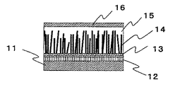
図1は、本発明による光電変換素子の一部の断面図である。基板11上に形成された第1の電極12とその上に形成されたナノチューブの支持層13に配向して植設されたナノチューブ14、ナノチューブを埋設する半導体層15、半導体層15に接して形成された第2の電極16から構成される。ナノチューブ14は、第1の電極12に直接電気的に接続されているか、導電性を付与された支持層13を介して第1の電極12に電気的に接続されている。
【0049】
ナノチューブの長さは、数10nmから数100μmの範囲で使用されるが、好ましい長さは、それぞれの半導体素子に求められる仕様によって異なる。例えば光電変換素子の場合で言えば、光電変換素子の半導体層に入射した光が吸収され、電荷が生成されるので、半導体層の厚さがナノチューブの長さを規定する。半導体層の厚さは、素子の効率の面から入射した光が十分吸収される厚さが必要である。通常、半導体層の光の吸収係数は102cm-1程度から大きくとも107cm-1程度であるので、例えば入射光の99%が吸収されるためには、半導体層の厚さは500μm程度から5nm程度必要である。直線的なナノチューブが、基板11の法線方向にほぼ平行に配向している場合、ナノチューブの長さは、半導体層の材料の膜厚とほぼ同程度の長さとなる。ただし、ナノチューブが斜めに配向している場合や、ナノチューブが曲がりくねっている場合には、半導体層から逸脱しない限り、さらに長くてもかまわない。
【0050】
ナノチューブの直径は、約1nmから数100nmのものが用いられるが、数nmから数10nmの直径が好ましい。例えばカーボンナノチューブの場合、最も小さいもので単層のナノチューブの約1nmから、層数が1増えるごとに直径が約0.7nmづつ増加する。ナノチューブの層数に応じて、直径数nmから100nmのものが用いられるが、数nmから数10nmの直径が好ましい。ナノチューブの密度が小さいと十分な電荷の捕集効率が得られず、大きすぎると半導体層の実質の体積が小さくなり、電荷の量が少なくなり、結果として十分な電荷を捕集できない。半導体材料の種類(特に、電子−正孔ペア(エキシトン)、電子、正孔の拡散距離)、ナノチューブの直径などに応じて、最適な密度が設定される。具体的には、ナノチューブ間の距離は、数nmから1μm、望ましくは、数nmから、数10nmである。
【0051】
ナノチューブの配向(度)は、直線的なナノチューブが、基板11の法線方向にほぼ平行に配向していても良いし、斜めに配向していてもかまわない。ナノチューブ間の距離が均一である方が望ましいので、ナノチューブの配向方向がそろっている方が望ましいが、そろっていなくてもかまわない。また、ナノチューブがらせん状や曲がりくねっていてもかまわない。
【0052】
<ナノチューブの植設方法>
本発明に用いられる電気的に電極に接続されたナノチューブの作製方法には、例えば以下のような方法がある。
【0053】
(1)既存のナノチューブを所望の長さに切断し、これを電気泳動法により電極上に配置する方法。
【0054】
電気泳動法は、ナノチューブを配置したい基板(電極)と、これに対して平行に対向して配置した対向電極との間に電圧を印加すると、電界に沿ってナノチューブが移動して基板(電極)に達する現象を利用したものである。一般には、ナノチューブを配向させて固定するために、支持層が用いられる。支持層としては、導電性を有し、細孔もしくは微細な隙間を有する層が好適に利用される。支持層は導電性であることが好ましい。また、電極自体が支持層を兼ねていてもかまわない。
【0055】
支持層の材料としては、多孔質の構造体、例えば、シリコンやアルミなどの陽極酸化膜、金、銀などの導電性微粒子の集合体膜などがある。また、ポリシランやPEDOT(ポリエチレンジオキシチオフェン)などの導電性高分子も支持層の材料として用いられる。また。高分子あるいは導電性高分子に良導体の微粒子を分散させた材料を使用しても良い。電気泳動法は、常温プロセスであるので、熱によるダメージを受けやすい基板への応用性や生産コストなどの面で望ましい。また、アーク放電法などで大量生産されたナノチューブを利用できるので、生産効率が良く、生産コストも低くなる。
【0056】
(2)化学的気相成長法(CVD法)により、炭素を含む原料ガスを基板表面に供給し、基板表面での化学反応によりナノチューブを成長させる方法。
【0057】
CVD法による方法は、基板上にFe、Ni、Fe−Ni合金、Co、Pdなどの触媒金属層(不連続なドット状でもかまわない)を形成し、加熱しながら、表面にアセチレン(C2H2)などのガス状の原料を供給すると、触媒金属の存在する部分にナノチューブが成長する現象を利用するものである。基板温度は、約600℃から800℃程度が好ましい。原料ガスとともに水素(H2)などのガスを流す場合もある。
【0058】
CVD法によれば、ナノチューブの密度は触媒金属の分布状況で制御でき、極めて密に、配向度の高いナノチューブが成長できる。触媒金属の分布状況をあらかじめ所望のパターンにしておくことで、そのパターンの領域にのみナノチューブを作製できる。ナノチューブの長さも、成長時間で制御できる。また、触媒金属の板や膜を基板として利用してもよい。
【0059】
<構成材料>
半導体層を構成する材料
半導体層を構成する材料としては、電子受容性機能を有する材料や電子受容性機能を有する材料であれば特に限定されないが、例えば以下の材料が利用されうる。
【0060】
電子受容性材料としては、ピリジン及びその誘導体を骨格にもつオリゴマーやポリマー、キノリン及びその誘導体を骨格にもつオリゴマーやポリマー、ベンゾフェナンスロリン類およびその誘導体によるラダーポリマー、シアノ−ポリフェニレンビニレンなどの高分子、フッ素化無金属フタロシアニン、フッ素化金属フタロシアニン類及びその誘導体、ペリレン及びその誘導体(PTCDA、PTCDIなど)、ナフタレン誘導体(NTCDA、NTCDAなど)、バソキュプロイン及びその誘導体などの低分子が利用されうる。
【0061】
電子供与性材料としてはチオフェン及びその誘導体を骨格にもつオリゴマーやポリマー、フェニレン−ビニレン及びその誘導体を骨格にもつオリゴマーやポリマー、チエニレン−ビニレン及びその誘導体を骨格にもつオリゴマーやポリマー、カルバゾール及びその誘導体を骨格にもつオリゴマーやポリマー、ビニルカルバゾール及びその誘導体を骨格にもつオリゴマーやポリマー、ピロール及びその誘導体を骨格にもつオリゴマーやポリマー、アセチレン及びその誘導体を骨格にもつオリゴマーやポリマー、イソチアナフェン及びその誘導体を骨格にもつオリゴマーやポリマー、ヘプタジエン及びその誘導体を骨格にもつオリゴマーやポリマーなどの高分子、無金属フタロシアニン、金属フタロシアニン類およびそれらの誘導体、ジアミン類、フェニルジアミン類およびそれらの誘導体、ペンタセンなどのアセン類およびその誘導体、ポルフィリン、テトラメチルポルフィリン、テトラフェニルポルフィリン、テトラベンズポルフィリン、モノアゾテトラベンズポルフィリン、ジアゾテトラベンズポルフィン、トリアゾテトラベンズポルフィリン、オクタエチルポルフィリン、オクタアルキルチオポルフィラジン、オクタアルキルアミノポルフィラジン、ヘミポルフィラジン、クロロフィル等の無金属ポルフィリンや金属ポルフィリン及びそれらの誘導体、シアニン色素、メロシアニン色素、スクアリリウム色素、キナクリドン色素、アゾ色素、アントラキノン、ベンゾキノン、ナフトキノン等のキノン系色素などの低分子が利用されうる。金属フタロシアニンや金属ポルフィリンの中心金属としては、マグネシウム、亜鉛、銅、銀、アルミニウム、ケイ素、チタン、バナジウム、クロム、マンガン、鉄、コバルト、ニッケル、スズ、白金、鉛などの金属、金属酸化物、金属ハロゲン化物が用いられる。
【0062】
半導体層としては、上記の材料が、単体でも用いられるが、上記材料が適当なバインダ材料に分散混合されたものを用いることも可能である。また、適当な高分子の主鎖中や側鎖に、上記の低分子を組み込んだ材料などが用いられる。前記のバインダ材料あるいは主鎖となる高分子としては、例えば、ポリカーボネート樹脂、ポリビニルアセタール樹脂、ポリエステル樹脂、変性エーテル型ポリエステル樹脂、ポリアリレート樹脂、フェノキシ樹脂、ポリ塩化ビニル樹脂、ポリ酢酸ビニル樹脂、ポリ塩化ビニリデン樹脂ポリスチレン樹脂、アクリル樹脂、メタクリル樹脂、セルロース樹脂、尿素樹脂、ポリウレタン樹脂、シリコン樹脂、エポキシ樹脂、ポリアミド樹脂、ポリアクリルアミド樹脂、ポリビニルアルコール樹脂などや、これらの共重合体、あるいは、ポリビニルカルバゾールやポリシランなどの光導電ポリマーなどが用いられる。
【0063】
半導体層には、前記の材料単体あるいは均一な混合物として利用できるが、電子供与性材料からなる領域と電子受容性材料からなる領域の接合構造を構成しても良い。
【0064】
ここで、接合構造とは、2種以上の異種の材料が接する界面(接合面)を有し、この界面(接合面)およびその近傍領域に生じる電子的作用により、素子としての特有の機能(整流、光電変換、発光など)を達成する構造を意味する。
【0065】
基板の材料
基板は、第1の電極が作製でき、安定に保持できるものであれば、材質や厚さは特に限定されない。例えば、ステンレスなど金属類や合金、ガラス、樹脂、紙、布などが挙げられる。光を基板側から入射させる場合には、素子で要求される波長範囲で所定の透明性を有する材料が用いられる。
【0066】
第1および第2の電極の材料
第1および第2の電極の材料としては、金、白金、アルミニウムなどの金属類、合金類、透明電極としては、例えば、酸化インジウムスズ(ITO)やフッ素ドープされた酸化スズ、酸化亜鉛、酸化錫等の金属酸化物が用いられる。ポリアセチレン、ポリピロール、ポリチアジルなどの導電性高分子を用いてもよい。電極材料は、透明性の他、半導体層との間の電気的性質(オーミック性やショットキー性など)によっても選択される。
【0067】
太陽電池などにおいて、第1および第2の電極の材料として透明導電膜を利用する場合には、通常、陰極側の仕事関数が陽極側よりも小さくする必要がある。仕事関数が小さい導電性金属酸化物は、例えばアルミニウム(Al)、マグネシウム(Mg)、カルシウム(Ca)、ストロンチウム(Sr)、バリウム(Ba)、リチウム(Li)等の仕事関数の小さい金属(すなわち4.3eV以下の金属)、または酸化アルミニウム(Al2O3)、酸化マグネシウム(MgO)や酸化バリウム(BaO)等の酸化物を、ITOやZnOなどの透明導電膜にドーパントとして微量添加することにより実現される。
【0068】
<製法>
まず基板11の上に第1の電極12を形成する。材料は例えば前述の材料が用いられる。第1の電極12の厚さは、十分な導電性が得られる厚さ以上あればよい。電極の作製方法は、特に限定はなく、例えば蒸着法、スパッタ法、CVD法、印刷法、スピンコート法などが用いられる。たとえば、代表的な透明導電膜であるITOの場合は、50nmから200nm程度あればよく、スパッタ法で作製される。必要に応じて、フォトリソグラフィーなどの公知の方法で電極をパターン化しても良い。次に、第1の電極12の表面にナノチューブ支持層13を形成し、支持層13にナノチューブ14を植設する。ナノチューブ14を植設する方法としては、前記のように、例えば電気泳動法やCVD法などが用いられる。電気泳動法の場合の支持層としては、前記の多孔質の構造体や導電性高分子が用いられる。多孔質の構造体は例えばシリコンやアルミニウムなどの陽極酸化で作製される。陽極酸化膜を作製するには公知の方法が採用可能である。例えば、容器内を化成液で満たし、半導体又は金属あるいは半導体基板又は金属膜を基板上に形成したものを陽極にし、対向電極を陰極にして対向して平行に配置し、電圧を印加すると、半導体又は金属の表面側に細孔を持つ陽極酸化膜が形成される。陽極酸化されていない部分はナノチューブと電極とを電気的に接続する機能を果たす。
【0069】
多孔質の構造体としては例えば導電性微粒子の集合体膜を利用することができる。導電性微粒子の集合体膜を作製するには公知の方法が採用可能である。例えば、金、銀、ニッケルなどの金属の微粒子をペースト状にして第1の電極上に塗布することで作製できる。加熱処理や、ペーストにエポキシ樹脂やアクリル樹脂などの高分子を混合するなどの方法により、微粒子の集合体膜の強度を高め、電極との密着性を高めることもできる。
【0070】
多孔質の構造体としては例えばポリシランやPEDOTなどの導電性高分子も支持層の材料として用いられる。また、高分子あるいは導電性高分子に良導体の微粒子を分散させた材料を使用しても良い。これらの支持層は、溶媒に溶かした高分子材料、あるいは高分子と良導体の微粒子の混合物をスピンコート法、スクリーン印刷などの塗布法で電極表面に形成できる。これらの高分子膜、高分子と良導体はそのままでも支持層として機能するが、紫外線や電子線などを照射することで、高分子鎖の一部の結合を切断して微細な隙間を形成したものを支持層として利用することも可能である。溶媒に溶かした高分子を用いて、支持層を形成した場合は、溶媒を高分子膜中から除去するために、加熱処理をしてもよい。温度は、溶媒の沸点程度の温度か、それ以上の温度が望ましい。処理時間は、高分子を用いた支持層の厚さに依存し、膜中の溶媒が十分除去されるまでの時間であることが望ましい。
【0071】
CVD法の場合、第1の電極12の表面に形成された触媒金属層が支持層の機能を果たす。触媒金属を用いたCVD法の場合、ナノチューブは触媒金属の微小な粒子を成長点として成長するので、ナノチューブは触媒金属に結合している。
【0072】
半導体層15の形成には、公知の技術が用いられる。例えば蒸着法、スパッタ法、CVD法、印刷法、スピンコート法などが用いられる。この他、溶媒中にミセルや微粒子を分散させた液を塗布し、溶媒を蒸発させる方法で半導体層15を形成してもかまわない。微粒子の製造には、気相成長法、粉砕法、再沈法、アシッドペースティング法などの公知の方法が利用できる。この他、半導体層15の形成には電界重合法を用いてもよい。半導体材料の原料となるモノマーあるいはオリゴマーを溶解させた溶液中に、前記のナノチューブを植設した構造体を浸漬して電源の一方の端子に第1の電極を接続し、別に溶液に浸漬した対向電極を電源の他方の端子に接続して対向して電圧をプラスマイナス数Vの範囲でスイープしながら印加すると、溶解していたモノマーあるいはオリゴマーが重合してナノチューブ表面に付着し、半導体層15が形成される。
【0073】
半導体層15の表面に第2の電極16を形成する方法は、例えば蒸着法、スパッタ法、CVD法、印刷法、スピンコート法などが用いられる。半導体層15に有機材料を用いた場合には、第2の電極の形成の際に半導体層表面にダメージが生じないようにすることが望ましい。例えば、第2の電極16形成の際のダメージの原因としては、熱があるが、これに対しては、第2の電極16形成の際に半導体層15を冷却してもよい。また、蒸着法における蒸着源のように、半導体層15の近くに熱源がある場合は、熱源からの輻射熱を遮蔽するための遮蔽版を熱源と半導体層15の間に配置してもよく、この場合は、遮蔽版を回り込んで半導体層15に達した物質により第2の電極は形成される。第2の電極16と半導体層15の間に、第2の電極16と半導体層15との間の電荷の移動を媒介する層を形成してもかまわない。
【0074】
(基本形態2)
第1の電極がナノチューブの支持層を兼ねた構成でも良い。一例を示す構成の断面図を図2に示す。
【0075】
<素子の構造>
基板21上に形成された第1の電極22とその上に配向して植設されるナノチューブ24、ナノチューブを埋設する半導体層25、半導体層に接して形成された第2の電極26から構成される。ナノチューブ24は、第1の電極22に接続されている。本実施の形態は、基本形態1における、支持層13がなく、ナノチューブ24が第1の電極22に直接植設されている点が異なり、基板、ナノチューブ、半導体層、第2の電極については、材料、製法共に基本形態1の記載と同様である。
【0076】
<製法>
基本形態1とは、支持層13がなく、ナノチューブ24が第1の電極22に直接配置されている点が異なるので、ナノチューブ24を第1の電極22に直接的に植設する方法についてのみ記載する。他の構成要素の製造方法は、基本形態1と同様である。
【0077】
第1の電極22に直接ナノチューブを植設する方法としては、例えば、化学的気相成長法(CVD法)により、炭素を含む原料ガスを基板表面に供給し、基板表面での化学反応によりナノチューブを成長させる方法を用いることができる。CVD法による方法では、Fe、Ni、Fe−Ni合金、Co、Pdなどの触媒金属層が成長表面に存在することが必要である。これらの金属は、通常、良好な導電性を示すので、基板上に形成された前記の触媒金属の層を第1の電極22とすることが可能である。基板21上に第1の電極22として触媒金属の層を形成したものを加熱しながら、表面にアセチレン(C2H2)などのガス状の原料を供給すると、触媒金属層上にナノチューブ24が成長する。基板温度は、約600℃から800℃程度が好ましい。原料ガスとともに不活性ガスや水素(H2)などのガスを流す場合もある。
【0078】
<効果>
本基本形態の方法によれば、ナノチューブの支持層を別に設ける必要がないので工程が簡便になる。CVD法によれば、ナノチューブの密度は触媒金属の分布状況で制御でき、極めて密に、配向度の高いナノチューブが成長できる。触媒金属の分布状況をあらかじめ所望のパターンにしておくことで、そのパターンの領域にのみナノチューブを作製できる。ナノチューブの長さも、成長時間で制御できる。
【0079】
(実施の形態1)
<素子の構造>
半導体層が電子供与性材料と電子受容性材料の2種の材料から構成される太陽電池において、電子供与性材料又は電子受容性材料でナノチューブがコートされている構造であってもかまわない。その一例を示す断面図を図3に示す。基板51の上に形成された第1の電極52と、その上に形成されたナノチューブの支持層53と、ナノチューブの支持層53に植設されたナノチューブ54と該ナノチューブ54をコートする電子供与性材料からなる領域551と、該電子供与性材料からなる領域551に接している電子受容性材料からなる領域552と、該電子受容性材料からなる領域552と直接接しているがナノチューブとは直接接していない第2の電極56から構成される。ナノチューブ54は、第1の電極52に直接に接続されているか、導電性を付与されたナノチューブの支持層53を介して第1の電極52に電気的に接続されている。
【0080】
図3では、電子供与性材料からなる領域551がナノチューブ54をコートしている構造の例を示したが、電子受容性材料からなる領域552がナノチューブをコートしている構造であってもかまわない。
【0081】
本実施の形態における材料は基本形態1の記載と同様である。また、ナノチューブは、図2に示す如く第1の電極に直接植設されていてもかまわない。ナノチューブを第1の電極に直接植設する形態および方法は、基本形態2に記載のとおりである。
【0082】
前記ナノチューブをコートする厚さは、半導体素子に必要とされる機能により決められるが、例えば光電変換素子では、入射光の波長分布、コートする材料の光の吸収係数、コートする材料内における電荷やエキシトンの移動可能距離(自由行程)などを勘案して決められ、1nm程度から数100nm程度の範囲である。
【0083】
<製法>
本発明の半導体素子において半導体層以外の製法は、基本形態1および2と同様である。本実施の形態のナノチューブ54は、電子供与性有機材料又は電子受容性有機材料でコートされている。ナノチューブを電子供与性有機材料又は電子受容性有機材料でコートする方法としては、例えば蒸着法、スパッタ法、CVD法、電界重合法などの公知の方法が用いられるが、特に有機材料においては電界重合法が好適に用いられる。電界重合法については、実施の形態1に記載のとおりである。電解重合膜の成長速度は、モノマー溶液の濃度などで制御でき、コートする厚さは、電界重合の時間などで制御できる。
【0084】
<効果>
ナノチューブのアスペクト比は非常に大きいので、接合面からナノチューブまでの距離、即ちコート材料の膜厚と、ナノチューブの密度を適当な値にすることにより、単に表面に対して平行な平面的接合と比較して、非常に大きな接合面積を得ることが出来る。また、接合面近傍で生成したキャリアあるいは接合面近傍に存在するキャリアは、コート材料の膜厚の距離を移動するだけでナノチューブに導かれる。ナノチューブは導電性に優れるため、ナノチューブに達して捕獲されたキャリアは効率的に電極まで達することが出来る。
【0085】
(実施の形態2)
<素子の構造>
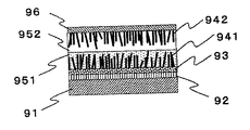
半導体層が電子供与性材料からなる層と電子受容性材料からなる層が積層されている構造でもかまわない。一例を示す断面図を図4に示す。半導体層が電子供与性材料からなる領域951の層と電子受容性材料からなる領域952の層の積層構造から構成されることを特徴とする。
【0086】
<製法>
本実施の形態の構成の素子は、基本形態1又は2記載の方法で半導体層の形成までを行った2つの構造体を、以下のように半導体層の面同士を張り合わせることで作製される。
【0087】
半導体層が、高分子である場合には、前記2つの構造体の半導体層の面同士を密着させた状態で、高分子からなる半導体のガラス転移点あるいは融点近傍の温度まで上げ、高分子に流動性を持たせた状態で一定時間圧着し、常温まで下げることで、前記2つの構造体を張り合わせることが可能である。高分子からなる半導体のガラス転移点あるいは融点近傍の温度に昇温し、保持し、室温に下げる工程は、不活性ガス雰囲気下、真空状態あるいは還元雰囲気であることが望ましく、また、光を遮断した状態であることも望ましい。別の張り合わせの方法としては、半導体層を構成する材料中に架橋剤を混ぜておくか、架橋性の官能基を導入しておき、前記2つの構造体の半導体層の面同士を密着させた状態で、熱、光などの架橋に必要なエネルギーを与え、2つの半導体同士を結合させることも可能である。また、光による架橋の場合において、半導体のガラス転移点あるいは融点近傍の温度まで上げた状態で一定時間圧着しつつ、光を照射してもよい。更に別の張り合わせの方法としては、前記2つの構造体の半導体層の面同士の間に両者を接着するための層を介在させてもよい。
【0088】
<効果>
本発明によれば、半導体層中で存在する(又は生成した)キャリアが拡散又はドリフトにより移動してナノチューブに到達するまでの距離を短く出来るので、半導体層に存在するキャリア或いは、半導体層で生成したキャリアを効率的かつ、高速に第1の電極及び第2の電極に導くことができるようになる。従って、デバイスの特性を向上できる。有機半導体は一般に無機半導体と比較してキャリアの移動度が低いが、本発明は、キャリアの移動距離を短くできるので、特に有効である。本実施の形態による光電変換素子では、電子供与性材料と電子受容性材料のエネルギー準位差により界面近傍に生成する内部電位差(ビルトイン電界)によって、効率的に電荷が生成できる。電荷の生成に必要な内部電位差の大きさは、電子供与性材料と電子受容性材料の組み合わせで制御できる。また、入射光の波長分布を電子供与性材料と電子受容性材料の2種の材料で相補的にカバーさせることができるので、入射光の利用効率が高まる。
【0089】
【実施例】
以下、実施の形態1〜2を実施例を用いて、さらに具体的に説明する。
【0090】
(実施例1)
実施の形態1の具体的な一例を示す。
【0091】
図3において基板51としては、ガラスを用い、表面に第1の電極52としてのITOをスパッタ法で膜厚約50nm形成する。ITO表面に、ナノチューブの支持層53として、高導電性のPEDOT膜を約50nmの厚さでスピンコート法により形成する。これを不活性ガス中(本例では窒素ガス中)で90℃で20分程度熱処理する。熱処理後ナノチューブ(長さ約1μm)をイソプロピルアルコール中に分散した液に浸漬し、平行に対向して配置した対向電極との間に電圧(約2KV/cm)を印加し、PEDOT上にナノチューブ54が表面に対してほぼ垂直に配向した構造体が得られる。
【0092】
この構造体を0.05Mのテトラブロモパラキシレン(tetrabromo−p−xylene)と0.1MのTEABF4と0.2%の水のDMF溶液に浸漬し、電界重合させると、ナノチューブ54表面及び支持層53露出部に電子供与性材料領域551としてポリフェニレンビニレン(polyphenylenevinylene)が形成される。本例の場合、膜厚はほぼ5nmであるが、電界重合の時間を適当に制御することにより、ポリフェニレンビニレン(polyphenylenevinylene)がナノチューブ54の表面全面、あるいは、一部をコートし、ナノチューブ54と隣接するナノチューブの間隙を埋め尽くしていない構造を形成することができる。
【0093】
この構造体に、ペリレン(perylene)の微粒子(粒子径 数nm〜数十nm)を分散させた液を塗布し、乾燥させるとポリフェニレンビニレン(polyphenylenevinylene)でコートされたナノチューブ同士の間隙にペリレン微粒子が充填され、ナノチューブの先端側にもペリレン微粒子が堆積されて、電子受容性材料領域552が形成される。
【0094】
第2の電極56は、電子受容性材料領域552の表面に数Åの厚さのAlLiまたはLiFを真空蒸着法で形成した後、真空を破ることなくAl電極を約50nm蒸着して、2層構造で構成される。以上の過程で光電変換素子が形成される。
【0095】
(実施例2)
実施の形態2の具体的な一例を示す。
【0096】
図4において基板91としては、ガラスを用い、表面に第1の電極92としてのITOをスパッタ法で膜厚約50nm形成する。ITO表面に、第1ナノチューブの支持層93として、高導電性のPEDOT膜を約50nmの厚さでスピンコート法により形成する。これを不活性ガス中(本例では窒素ガス中)で90℃で20分程度熱処理する。熱処理後ナノチューブ(長さ約1μm)をイソプロピルアルコール中に分散した液に浸漬し、平行に対向して配置した対向電極との間に電界(約2KV/cm)を印加すると、PEDOT上に第1ナノチューブ941が表面に対してほぼ垂直に配向した構造体が得られる。この構造体上に電子供与性有機材料であるポリフェニレンビニレン(polyphenylenevinylene)の誘導体MEH−PPVをキシレンに溶解させた溶液(約0.5重量%)を用いてスピンコート法でMEH−PPVの薄膜を作製する。
【0097】
第2の電極96としてFe-Ni合金基板を用い、これを約700℃に加熱し、表面にアセチレン(C2H2)と水素(H2)の混合ガスを供給すると第2ナノチューブ942がほぼ基板に垂直配向して成長する。
【0098】
この構造体上に電子受容性有機材料であるポリフェニレンビニレン(polyphenylenevinylene)の誘導体のCN−PPVをキシレンに溶解させた溶液(約0.5重量%)を用いてスピンコート法でCN−PPVの薄膜を作製する。
【0099】
前記の基板91上の構造体と、前記の第2の電極96上の構造体をMEH−PPVとCN−PPVの膜の面同士で接しさせて、窒素雰囲気下でガラス転移点温度近傍まで加熱するとMEH−PPVとCN−PPVとが密着し、図4に示す構造の素子が形成できる。
【0100】
【発明の効果】
本発明によれば、半導体層で生成したキャリアを効率的かつ、高速に電極に導くことができるようになる。従って、デバイスの特性を向上できる。有機半導体は一般に無機半導体と比較してキャリアの移動度が低いが、本発明によればキャリアの移動距離を短くできるので、半導体層として有機半導体を用いる場合、本発明は特に有効である。
【0101】
また、有機材料を用いることにより、本発明に関する構造を利用したデバイスを形成するためのプロセスを簡単かつ低コストにすることが可能になる。
【図面の簡単な説明】
【図1】 本発明の一実施の形態である光電変換素子の一部の断面図である。
【図2】 本発明の一実施の形態である光電変換素子の一部の断面図である。
【図3】 本発明の一実施の形態である光電変換素子の断面図である。
【図4】 本発明の一実施の形態である光電変換素子の断面図である。
【符号の説明】
11,21,51,91 基板、12,22,52,92 第1の電極、13,53,93 支持層、14,24,54 ナノチューブ、941 第1ナノチューブ、942 第2ナノチューブ、15,25 半導体層、551,951 電子供与性材料からなる領域、552,952 電子受容性材料からなる領域、16,26,56,96 第2の電極。[0001]
BACKGROUND OF THE INVENTION
The present invention relates to a semiconductor element such as a photoelectric conversion element such as a solar cell, a light emitting element, a light receiving element, a diode, a transistor, a sensor, or an imaging element.
[0002]
[Prior art]
In recent years, with the spread of mobile devices such as portable terminals and notebook computers and the seriousness of environmental problems such as reduction of energy consumption, there is an increasing demand for devices with high energy utilization efficiency. Also in a semiconductor device, efficient generation and efficient movement of charges are the most important elements for improving device performance. In addition, the price of electronic equipment has been reduced, and not only high-performance devices and systems have high efficiency and high functionality, but also there has been a great demand for technologies that can be produced at low cost.
[0003]
Various techniques have been proposed for this purpose. Here, a solar cell that is a photoelectric conversion element will be described as an example.
[0004]
The prior art discloses a heterojunction functional device (diode, solar cell) in which fullerene and a derivative are dispersed in a conjugated polymer (see Patent Document 1, page 14). Electron-hole pairs excited by incident light are generated by a structure in which an infinite number of bonding surfaces of electron-donating materials consisting of fullerenes and derivatives, which are electron-accepting materials, and conjugated polymers exist at intervals of nanometer order. The purpose is to efficiently separate and generate carriers. However, at present, the mobility of organic materials and fullerene aggregates is very small compared to inorganic materials, so when carriers generated in the semiconductor layer move to the electrode, there are large losses due to trapping and deactivation, The carrier is not being used effectively.
[0005]
In addition, in order to efficiently collect photogenerated carriers and move them to the electrode, it is composed of at least an electron-accepting transport layer, a donating transport layer, and an intervening light absorbing layer. A technique is disclosed in which either of the transport layers itself is a semiconductor needle crystal (see
[0006]
Furthermore, a technique is disclosed in which at least an electron-accepting transport layer, an electron-donating transport layer, and an intervening light absorption layer are formed, and either the electron-accepting transport layer or the electron-donating transport layer itself is a flaky semiconductor crystal. (See Patent Document 3, page 4).
[0007]
Also disclosed is a technique for transporting the charge generated by the photoelectric conversion means by a needle-shaped semiconductor crystal connected to one of the electrodes, and forming the needle-shaped semiconductor crystal by an electrodeposition method. (See Patent Documents 4, 4 and 6-7).
[0008]
In addition, it is a technique for transporting the charge generated by the photoelectric conversion means through a needle crystal connected to one of the electrodes, and the needle crystal is formed by an electrodeposition method, and the needle crystal has a granular semiconductor crystal. Is disclosed (see Patent Literature 5, pages 4 to 6).
[0009]
Furthermore, similarly, a technique is disclosed in which a columnar film formed on a substrate and generated by the deposition of a vapor deposition material flying from a direction inclined at a predetermined angle from the normal direction of the substrate is used as a charge collection electrode ( (See Patent Document 6,
[0010]
These all have the effect that the effective surface area of the electrode is increased, and the device characteristics can be improved by improving the efficiency and speed of charge transfer.
[0011]
However, the techniques disclosed in these
[0012]
In addition, in the technology using the columnar film as the charge collection electrode, the columnar crystal is not a general vapor phase growth method such as PVD or CVD, but uses a unique columnar structure obtained by dynamic oblique deposition. (See Patent Document 6,
[0013]
[Patent Document 1]
JP-T 8-500701
[0014]
[Patent Document 2]
JP 2001-93590 A
[0015]
[Patent Document 3]
JP 2001-358347 A
[0016]
[Patent Document 4]
JP 2002-93471 A
[0017]
[Patent Document 5]
JP 2002-141115 A
[0018]
[Patent Document 6]
JP 2002-170557 A
[0019]
[Problems to be solved by the invention]
As described above, several technologies that enable efficient generation and efficient transfer of charges in semiconductor elements, particularly semiconductor elements using organic materials, have been proposed. Productivity could not be realized. The present invention provides the aboveProblems with conventional technologyIn view of the above, it is possible to efficiently generate and move charges, and to improve device performance such as conversion efficiency and luminous efficiency.ButAn object of the present invention is to provide a semiconductor element useful for realizing an electronic device that is excellent and can be easily manufactured at low cost, and a method for manufacturing the same.
[0020]
[Means for Solving the Problems]
In order to solve the above problems, a semiconductor element of the present invention includes a first electrode, a nanotube electrically connected to the first electrode, a semiconductor layer in contact with the nanotube, and the semiconductor layer. Is a semiconductor element composed of a second electrode that is electrically connected to the nanotube and is not in direct contact with the nanotube.
[0021]
The nanotube in the present invention means a tube-like or tube-filled structure, is conductive at least in the long axis direction, and has an outer diameter of about 1 nm to several hundred nm. Furthermore, the structure of a cylindrical structure in which sheets of atoms and molecules are rolled, and a structure in which structures of different diameters are concentrically overlapped, the outermost cylindrical structure has a diameter of about 1 nm to several hundred nm. Means things. As a suitable structure, there is a structure in which a graphite sheet structure made of carbon is formed into a cylindrical shape as a basic structure. Another suitable structure has a cylindrical structure of a sheet structure made of amorphous carbon as a basic structure. According to the present invention, since the distance until carriers existing (or generated) in the semiconductor layer move by diffusion or drift and reach the nanotube can be shortened, carriers generated in the semiconductor layer or generated in the semiconductor layer The carrier thus made can be efficiently and rapidly guided to the first electrode. Therefore, the device characteristics can be improved. In particular, when an organic semiconductor is used as the semiconductor layer, an organic semiconductor generally has a lower carrier mobility than an inorganic semiconductor. Therefore, when an organic semiconductor is used, the carrier movement distance can be shortened.
[0022]
As still another embodiment, the semiconductor layer may be composed of two materials, an electron donating material and an electron accepting material. For example, since the distance until the carrier generated at the junction between the electron-donating organic material and the electron-accepting organic material reaches the nanotube can be shortened, the generated carrier can be efficiently and rapidly guided to the first electrode. become able to. Therefore, the device characteristics can be improved.
[0023]
When the semiconductor layer is composed of two types of materials, an electron donating material and an electron accepting material, the electron donating region and the electron accepting region are mixed, and the contact surface (bonding surface) of both is complicated. It is also possible to have a structure in which nanotubes are formed so as to penetrate through the joint surface and are connected to electrodes. In this case, a very large bonding area can be obtained as compared with planar bonding simply parallel to the surface. In addition, since the carriers generated near the bonding surface or the carriers existing near the bonding surface reach the nanotube only by moving a short distance, the nanotube is excellent in conductivity, so that the carrier captured by the nanotube efficiently reaches the electrode. Can reach.
[0024]
Moreover, the surface of the nanotube may be coated with either an electron-donating material or an electron-accepting material, and the other may be arranged so as to be in contact with the coated material. Since the aspect ratio of nanotubes is very large, by simply setting the distance from the bonding surface to the nanotubes (that is, the film thickness of the coating material) and the density of the nanotubes to an appropriate value, planar bonding that is only parallel to the surface can be achieved. In comparison, a very large bonding area can be obtained. In addition, carriers generated in the vicinity of the bonding surface or carriers existing in the vicinity of the bonding surface reach the nanotube only by moving the distance of the film thickness of the coating material. Can reach the electrode efficiently.
[0025]
Further, the electron donating material or the electron accepting material constituting the semiconductor layer may be composed of fine particles, or the semiconductor layer may be manufactured using the starting material as fine particles. By using fine particles, a structure in which the region of the electron donating material and the region of the electron accepting material are complicated can be easily manufactured. In addition, for example, a material that does not have a suitable solvent and can be produced only by a normal vapor deposition method can be used to produce a thin film by, for example, applying a liquid or paste-like sample in which fine particles are dispersed in a solvent onto a substrate. Thus, the manufacturing method becomes simple.
[0026]
You may comprise the said semiconductor layer with the material which forms a Schottky junction with respect to a nanotube. For example, the Schottky barrier region generated near the interface between the nanotube and the semiconductor layer functions to dissociate electron-hole pairs (excitons) generated by photoexcitation of the semiconductor layer into electrons and holes. Since the aspect ratio of nanotubes is very large, by setting the density of the nanotubes to an appropriate value, a very large bonding area can be obtained as compared with planar bonding simply parallel to the surface. Carriers generated in the vicinity of the bonding surface or carriers existing in the vicinity of the bonding surface are guided to the nanotube. Since the nanotube is excellent in conductivity and mobility, the carrier captured by the nanotube can efficiently reach the electrode.
[0027]
The semiconductor layer may be in contact with the nanotube through a material that forms a Schottky junction with the semiconductor layer.
[0028]
Since the aspect ratio of the nanotube is very large, the distance from the Schottky junction surface to the nanotube, that is, the thickness of the material forming the Schottky junction with respect to the semiconductor layer and the density of the nanotube are set to appropriate values. Compared with planar bonding that is simply parallel to the surface, a very large bonding area can be obtained. In addition, since nanotubes exist at a distance of the film thickness of the material that forms a Schottky junction with respect to the semiconductor layer with respect to any bonding surface, carriers generated near the bonding surface or carriers existing near the bonding surface are Just by moving a short distance, it is efficiently guided to the nanotube. Since the nanotubes are excellent in conductivity, carriers captured by the nanotubes can efficiently reach the electrodes.
[0029]
Further, the material for forming the Schottky junction with the semiconductor layer may be made of fine particles, or the starting material may be made of fine particles. In addition, by using fine particles, for example, a material without an appropriate solvent, and a material in which a thin film can be formed only by a normal vapor deposition method, for example, a liquid or pasty sample in which fine particles are dispersed in a solvent is applied on a substrate. A thin film can be produced by this method, and the production method becomes simple.
[0030]
A first electrode, a first nanotube electrically connected to the first electrode, a second electrode, a second nanotube electrically connected to the second electrode, a first nanotube, The semiconductor layer may include a semiconductor layer in which the second nanotube is embedded, and the first nanotube and the second nanotube may not be in contact with each other.
[0031]
According to the present invention, since the distance until carriers existing (or generated) in the semiconductor layer move by diffusion or drift and reach the nanotube can be shortened, carriers generated in the semiconductor layer or generated in the semiconductor layer The carriers thus introduced can be efficiently and quickly guided to the first electrode and the second electrode. Therefore, the device characteristics can be improved. Since organic semiconductors generally have lower carrier mobility than inorganic semiconductors, the present invention is particularly effective when organic semiconductors are used.
[0032]
A first electrode, a first nanotube electrically connected to the first electrode, a second electrode, a second nanotube electrically connected to the second electrode, a first nanotube, The semiconductor element may be composed of a semiconductor layer in which the second nanotube is embedded, and may include a support layer for implanting the nanotube in the semiconductor element that is not in contact with the first nanotube. With this configuration, the nanotube can be firmly fixed on the electrode. Further, by using a conductive material as the material for the nanotube support layer, the electrical contact between the nanotube and the electrode can be enhanced.
[0033]
A first electrode, a first nanotube electrically connected to the first electrode, a second electrode, a second nanotube electrically connected to the second electrode, a first nanotube, In the semiconductor element comprising a semiconductor layer in which the second nanotube is embedded, and the first nanotube and the second nanotube are not in contact with each other, the semiconductor layer is divided into two types of an electron donating material and an electron accepting material. You may comprise from material. For example, since the distance at which the carriers generated at the junction between the electron-donating organic material and the electron-accepting organic material reach the nanotube can be shortened, the generated carriers can be efficiently and quickly transferred to the first electrode and the second electrode. It can be led to the electrode. Therefore, the device characteristics can be improved.
[0034]
When the semiconductor layer is composed of two types of materials, an electron donating material and an electron accepting material, the electron donating region and the electron accepting region are mixed, and the contact surface (joint surface) of both is complicated. It may be a structure in which a structure is formed, and nanotubes existing so as to penetrate the joint surface are connected to electrodes. In this case, a very large bonding area can be obtained as compared with planar bonding simply parallel to the surface. In addition, since the carriers generated near the bonding surface or the carriers existing near the bonding surface reach the nanotube only by moving a short distance, the nanotube is excellent in conductivity, so that the carrier captured by the nanotube efficiently reaches the electrode. Can reach.
[0035]
Alternatively, the surface of the nanotube may be coated with either an electron-donating material or an electron-accepting material, and the other material may be disposed in contact with the coated material. Since the aspect ratio of nanotubes is very large, by simply setting the distance from the bonding surface to the nanotubes (that is, the film thickness of the coating material) and the density of the nanotubes to an appropriate value, planar bonding that is only parallel to the surface can be achieved. In comparison, a very large bonding area can be obtained. In addition, carriers generated in the vicinity of the bonding surface or carriers existing in the vicinity of the bonding surface reach the nanotube only by moving the distance of the film thickness of the coating material. Can reach the electrode efficiently.
[0036]
Further, the electron donating material or the electron accepting material constituting the semiconductor layer may be composed of fine particles, or the semiconductor layer may be manufactured using the starting material as fine particles. By using fine particles, a structure in which the region of the electron donating material and the region of the electron accepting material are complicated can be easily manufactured. In addition, for example, a material that does not have a suitable solvent and can be produced only by a normal vapor deposition method can be used to produce a thin film by, for example, applying a liquid or paste-like sample in which fine particles are dispersed in a solvent onto a substrate. Thus, the manufacturing method becomes simple.
[0037]
You may comprise a semiconductor layer with the material which forms a Schottky junction with respect to a nanotube. For example, the Schottky barrier region generated near the interface between the nanotube and the semiconductor layer functions to dissociate electron-hole pairs (excitons) generated by photoexcitation of the semiconductor layer into electrons and holes. Since the aspect ratio of nanotubes is very large, by setting the density of the nanotubes to an appropriate value, a very large bonding area can be obtained as compared with planar bonding simply parallel to the surface. Carriers generated in the vicinity of the bonding surface or carriers existing in the vicinity of the bonding surface are guided to the nanotube. Since the nanotube is excellent in conductivity and mobility, the carrier captured by the nanotube can efficiently reach the electrode.
[0038]
Since the work function of the nanotube can be controlled by the surface treatment of the nanotube, it is possible to make a difference between the work function of the first nanotube and the work function of the second nanotube. For example, by appropriately setting the work functions of the first nanotube, the second nanotube, and the semiconductor layer, the semiconductor layer forms a Schottky junction for one nanotube and an ohmic junction for the other. It is also possible to make it.
[0039]
The semiconductor layer may be in contact with the nanotube through a material that forms a Schottky junction with the semiconductor layer. Since the aspect ratio of nanotubes is very large, by simply setting the distance from the bonding surface to the nanotubes (that is, the film thickness of the coating material) and the density of the nanotubes to an appropriate value, planar bonding that is only parallel to the surface can be achieved. In comparison, a very large bonding area can be obtained. In addition, carriers generated in the vicinity of the bonding surface or carriers existing in the vicinity of the bonding surface reach the nanotube only by moving the distance of the film thickness of the coating material. Can reach the electrode efficiently.
[0040]
Further, the material for forming the Schottky junction with the semiconductor layer may be made of fine particles, or the starting material may be made of fine particles. In addition, by using fine particles, for example, a material without an appropriate solvent, and a material in which a thin film can be formed only by a normal vapor deposition method, for example, a liquid or pasty sample in which fine particles are dispersed in a solvent is applied on a substrate. A thin film can be produced by this method, and the production method becomes simple.
[0041]
In the present invention, electrophoresis may be used as a method for arranging nanotubes (including first and second nanotubes) at predetermined positions. By using the electrophoresis method, an expensive facility such as a vacuum process, a heat treatment, or a plasma process is required, and a simple and low-cost manufacturing process can be realized without going through a process with high energy consumption. Since the electrophoresis method is a normal temperature process, nanotubes can be arranged on the surface of a structure including a material that is easily damaged by heat. In addition, according to the electrophoresis method, it is possible to align the nanotubes in almost one direction.
[0042]
In the present invention, a CVD method may be used as a method for producing a nanotube. According to the CVD method, it is possible to grow the nanotubes so as to be substantially perpendicular to the substrate, and to easily control the density of the nanotubes. In the vacuum deposition method, atoms or molecules constituting a thin film to be produced are supplied onto the substrate, so that it is generally difficult to form nanotubes on the substrate surface. In contrast, the CVD method can produce nanotubes by supplying carbon-containing molecules to the substrate surface and using the thermally induced reaction, catalytic chemical reaction, plasma reaction, or a combination of these on the surface. As a method for performing this, it is a preferred method among vapor phase growth methods. A chemical reaction using a catalytic metal or the like that is arranged in advance on the substrate surface is mainly used.
[0043]
The semiconductor layer, the region made of the electron donating material, and the region made of the electron accepting material can be formed by polymerization from a monomer. By supplying a monomer in the form of gas or solution to the surface of the nanotube and polymerizing it, a structure in which the polymer is coated on the surface of the nanotube or a structure in which the nanotube is embedded in the polymer can be easily produced. Of course, a polymer organic semiconductor solution may be supplied to the substrate on which the nanotubes are arranged to form a structure in which the polymer organic semiconductor is in contact with the nanotubes. Due to viscosity and surface tension, the polymer semiconductor may not sufficiently penetrate into the gap between the nanotubes. On the other hand, in the case of a monomer, since the monomer molecule is small, it can enter the gap between the nanotubes and easily reach the surface of the nanotube. Therefore, a method by polymerization from the monomer is preferable.
[0044]
Among the methods of forming the semiconductor layer, the region made of the electron donating material, and the region made of the electron accepting material by polymerization from a monomer, the electric field polymerization method is more preferably used. The electropolymerization method is a method of generating a polymer on the surface of a nanotube by immersing an electrode substrate on which the nanotube is arranged in a solution of a monomer of an organic semiconductor and applying an electric field. According to this method, the monomer solution penetrates into the minute gaps of the nanotubes and forms a polymer on the surface of the nanotubes, so that the polymer can be formed on the entire surface of the nanotubes. Moreover, since the film thickness of the polymer can be controlled by controlling the growth time, for example, the nanotube surface can be coated with the polymer. Moreover, since the electric field is simply applied by immersing in the monomer solution, the apparatus is very simple as compared with a method such as vapor deposition.
[0045]
DETAILED DESCRIPTION OF THE INVENTION
Hereinafter, the semiconductor device according to the present invention will be described.Basic form andEmbodiments will be described.
[0046]
The present invention can be used for semiconductor elements in general, but can be suitably used for photovoltaic elements such as solar cells, photoelectric conversion elements used for optical sensors, photodiodes, and the like. Therefore, although embodiment of this invention is described in detail using the Example of a solar cell or a photoelectric conversion element, this invention is not limited to these Examples.
[0047]
The photoelectric conversion elements of the following
[0048]
(Basic form1)
<Element structure>
FIG. 1 shows a photoelectric conversion element according to the present invention.Part ofIt is sectional drawing. Formed in contact with the
[0049]
The length of the nanotube is used in the range of several tens of nm to several hundreds of μm, but the preferred length varies depending on the specifications required for each semiconductor element. For example, in the case of a photoelectric conversion element, light incident on the semiconductor layer of the photoelectric conversion element is absorbed and a charge is generated, so the thickness of the semiconductor layer defines the length of the nanotube. The thickness of the semiconductor layer needs to be a thickness that allows the incident light to be sufficiently absorbed from the aspect of efficiency of the element. Usually, the light absorption coefficient of the semiconductor layer is 102cm-1About 10 at most7cm-1Therefore, for example, in order to absorb 99% of incident light, the thickness of the semiconductor layer needs to be about 500 μm to about 5 nm. When the linear nanotubes are oriented substantially parallel to the normal direction of the
[0050]
Nanotubes having a diameter of about 1 nm to several hundreds nm are used, but a diameter of several nm to several tens of nm is preferable. For example, in the case of carbon nanotubes, the diameter increases from about 1 nm of the smallest single-walled nanotube by about 0.7 nm as the number of layers increases by one. Depending on the number of nanotube layers, a diameter of several nm to 100 nm is used, but a diameter of several nm to several tens of nm is preferable. If the density of the nanotubes is small, sufficient charge collection efficiency cannot be obtained, and if it is too large, the substantial volume of the semiconductor layer is reduced, the amount of charges is reduced, and as a result, sufficient charges cannot be collected. The optimum density is set according to the type of semiconductor material (in particular, electron-hole pair (exciton), electron and hole diffusion distance), the diameter of the nanotube, and the like. Specifically, the distance between the nanotubes is several nm to 1 μm, preferably several nm to several tens of nm.
[0051]
Regarding the orientation (degree) of the nanotube, the linear nanotube may be oriented substantially parallel to the normal direction of the
[0052]
<Method of planting nanotubes>
For example, the following method can be used as a method for producing a nanotube electrically connected to an electrode used in the present invention.
[0053]
(1) A method in which an existing nanotube is cut into a desired length and placed on an electrode by electrophoresis.
[0054]
In the electrophoresis method, when a voltage is applied between a substrate (electrode) on which nanotubes are to be arranged and a counter electrode arranged in parallel with the substrate, the nanotubes move along the electric field and move to the substrate (electrode). It uses the phenomenon that reaches In general, a support layer is used to align and fix the nanotubes. As the support layer, a layer having conductivity and having pores or fine gaps is preferably used. The support layer is preferably conductive. The electrode itself may also serve as the support layer.
[0055]
Examples of the material for the support layer include a porous structure, for example, an anodized film such as silicon and aluminum, and an aggregate film of conductive fine particles such as gold and silver. In addition, a conductive polymer such as polysilane or PEDOT (polyethylenedioxythiophene) is also used as a material for the support layer. Also. A material in which fine particles of a good conductor are dispersed in a polymer or a conductive polymer may be used. Since the electrophoresis method is a room temperature process, it is desirable in terms of application to a substrate that is easily damaged by heat, production cost, and the like. In addition, since nanotubes mass-produced by an arc discharge method or the like can be used, production efficiency is good and production cost is low.
[0056]
(2) A method in which a source gas containing carbon is supplied to the substrate surface by chemical vapor deposition (CVD), and nanotubes are grown by a chemical reaction on the substrate surface.
[0057]
In the CVD method, a catalytic metal layer (such as discontinuous dots) such as Fe, Ni, Fe—Ni alloy, Co, and Pd is formed on a substrate, and acetylene (C2H2When a gaseous raw material such as) is supplied, a phenomenon in which nanotubes grow in a portion where a catalytic metal exists is utilized. The substrate temperature is preferably about 600 ° C. to 800 ° C. Hydrogen (H2) Etc. may flow.
[0058]
According to the CVD method, the density of the nanotubes can be controlled by the distribution state of the catalytic metal, and nanotubes with a high degree of orientation can be grown very densely. By making the distribution state of the catalyst metal into a desired pattern in advance, nanotubes can be produced only in the region of the pattern. The length of the nanotube can also be controlled by the growth time. Further, a catalyst metal plate or film may be used as the substrate.
[0059]
<Constituent materials>
Materials constituting the semiconductor layer
The material constituting the semiconductor layer is not particularly limited as long as it is a material having an electron accepting function or a material having an electron accepting function. For example, the following materials can be used.
[0060]
Examples of the electron-accepting material include oligomers and polymers having pyridine and its derivatives as a skeleton, oligomers and polymers having quinoline and its derivatives as a skeleton, ladder polymers made of benzophenanthrolines and derivatives thereof, and cyano-polyphenylene vinylene. Small molecules such as molecules, fluorinated metal-free phthalocyanines, fluorinated metal phthalocyanines and derivatives thereof, perylene and derivatives thereof (PTCDA, PTCDI, etc.), naphthalene derivatives (NTCDA, NTCDA, etc.), bathocuproin and derivatives thereof can be used.
[0061]
As electron donating materials, oligomers and polymers having thiophene and its derivatives as a skeleton, oligomers and polymers having phenylene-vinylene and its derivatives as a skeleton, oligomers and polymers having thienylene-vinylene and its derivatives as a skeleton, carbazole and its derivatives Oligomers and polymers having skeletons, oligomers and polymers having skeletons of vinylcarbazole and derivatives thereof, oligomers and polymers having skeletons of pyrrole and derivatives thereof, oligomers and polymers having skeletons of acetylene and derivatives thereof, isothiaphene and its Oligomers and polymers with derivatives as skeletons, polymers such as oligomers and polymers with skeletons of heptadiene and derivatives thereof, metal-free phthalocyanines, metal phthalocyanines and their derivatives, diamines Phenyldiamines and derivatives thereof, acenes such as pentacene and derivatives thereof, porphyrin, tetramethylporphyrin, tetraphenylporphyrin, tetrabenzporphyrin, monoazotetrabenzporphyrin, diazotetrabenzporphine, triazotetrabenzporphyrin, octaethylporphyrin , Octaalkylthioporphyrazine, octaalkylaminoporphyrazine, hemiporphyrazine, metalloporphyrin and metalloporphyrin and their derivatives such as chlorophyll, cyanine dye, merocyanine dye, squarylium dye, quinacridone dye, azo dye, anthraquinone, benzoquinone, naphthoquinone Small molecules such as quinone dyes such as can be used. As the central metal of metal phthalocyanine and metal porphyrin, magnesium, zinc, copper, silver, aluminum, silicon, titanium, vanadium, chromium, manganese, iron, cobalt, nickel, tin, platinum, lead and other metals, metal oxides, Metal halides are used.
[0062]
As the semiconductor layer, the above materials can be used alone, but it is also possible to use a material obtained by dispersing and mixing the above materials in an appropriate binder material. Moreover, the material etc. which incorporated said low molecule in the principal chain or side chain of a suitable polymer are used. Examples of the binder material or the main chain polymer include polycarbonate resin, polyvinyl acetal resin, polyester resin, modified ether type polyester resin, polyarylate resin, phenoxy resin, polyvinyl chloride resin, polyvinyl acetate resin, poly Vinylidene chloride resin Polystyrene resin, acrylic resin, methacrylic resin, cellulose resin, urea resin, polyurethane resin, silicone resin, epoxy resin, polyamide resin, polyacrylamide resin, polyvinyl alcohol resin, etc., copolymers thereof, or polyvinyl carbazole And photoconductive polymers such as polysilane are used.
[0063]
The semiconductor layer can be used as a single material or a uniform mixture of the above materials, but a junction structure of a region made of an electron donating material and a region made of an electron accepting material may be formed.
[0064]
Here, the bonding structure has an interface (bonding surface) at which two or more different kinds of materials are in contact, and an electronic function generated at this interface (bonding surface) and its vicinity region (function unique to the element ( Rectification, photoelectric conversion, light emission, etc.).
[0065]
Substrate material
The material and thickness of the substrate are not particularly limited as long as the first electrode can be manufactured and can be stably held. Examples thereof include metals such as stainless steel, alloys, glass, resin, paper, and cloth. When light is incident from the substrate side, a material having a predetermined transparency in a wavelength range required by the element is used.
[0066]
Material for first and second electrodes
As materials of the first and second electrodes, metals such as gold, platinum, and aluminum, alloys, and as transparent electrodes, for example, indium tin oxide (ITO), fluorine-doped tin oxide, zinc oxide, oxidation A metal oxide such as tin is used. Conductive polymers such as polyacetylene, polypyrrole, and polythiazyl may be used. The electrode material is selected not only by transparency but also by electrical properties (such as ohmic property and Schottky property) with the semiconductor layer.
[0067]
When a transparent conductive film is used as a material for the first and second electrodes in a solar cell or the like, it is usually necessary to make the work function on the cathode side smaller than that on the anode side. The conductive metal oxide having a small work function is, for example, a metal having a low work function such as aluminum (Al), magnesium (Mg), calcium (Ca), strontium (Sr), barium (Ba), lithium (Li) (ie, 4.3 eV or less metal) or aluminum oxide (Al2OThree), Magnesium oxide (MgO), barium oxide (BaO), and other oxides are added as a dopant to a transparent conductive film such as ITO or ZnO.
[0068]
<Production method>
First, the
[0069]
As the porous structure, for example, an aggregate film of conductive fine particles can be used. A well-known method can be adopted to produce an aggregate film of conductive fine particles. For example, it can be produced by applying fine particles of metal such as gold, silver, nickel, etc. on the first electrode in the form of a paste. The strength of the aggregate film of fine particles can be increased and the adhesion to the electrode can be increased by heat treatment or a method such as mixing a polymer such as an epoxy resin or an acrylic resin with the paste.
[0070]
As the porous structure, for example, a conductive polymer such as polysilane or PEDOT is also used as a material for the support layer. Further, a material in which fine particles of a good conductor are dispersed in a polymer or a conductive polymer may be used. These support layers can be formed on the electrode surface by applying a polymer material dissolved in a solvent or a mixture of polymer and fine particles of a good conductor by a spin coating method, screen printing or the like. These polymer films, polymers and good conductors can function as a support layer as they are, but by irradiating them with ultraviolet rays or electron beams, some bonds in the polymer chains are cut to form fine gaps. Can also be used as a support layer. When the support layer is formed using a polymer dissolved in a solvent, heat treatment may be performed in order to remove the solvent from the polymer film. The temperature is preferably about the boiling point of the solvent or higher. The treatment time depends on the thickness of the support layer using the polymer, and is desirably the time until the solvent in the membrane is sufficiently removed.
[0071]
In the case of the CVD method, the catalytic metal layer formed on the surface of the
[0072]
A known technique is used to form the
[0073]
As a method for forming the
[0074]
(Basic form2)
The first electrode may also serve as a nanotube support layer. A cross-sectional view of an example configuration is shown in FIG.
[0075]
<Element structure>
The
[0076]
<Production method>
Basic form1 is different in that the
[0077]
As a method of implanting nanotubes directly on the
[0078]
<Effect>
BookBasic formAccording to the method, it is not necessary to separately provide a nanotube support layer, and thus the process is simplified. According to the CVD method, the density of the nanotubes can be controlled by the distribution state of the catalytic metal, and nanotubes with a high degree of orientation can be grown very densely. By making the distribution state of the catalyst metal into a desired pattern in advance, nanotubes can be produced only in the region of the pattern. The length of the nanotube can also be controlled by the growth time.
[0079]
(Embodiment1)
<Element structure>
In the solar cell in which the semiconductor layer is composed of two materials of an electron donating material and an electron accepting material, a structure in which a nanotube is coated with an electron donating material or an electron accepting material may be used. A cross-sectional view showing an example3Shown in A
[0080]
Figure3In the above example, the
[0081]
The material in this embodiment isBasic form1 is the same as described above. Further, the nanotubes may be directly implanted in the first electrode as shown in FIG. The form and method of implanting the nanotubes directly on the first electrode is:Basic form2 as described.
[0082]
The thickness for coating the nanotube is determined by the function required for the semiconductor element. For example, in the photoelectric conversion element, the wavelength distribution of incident light, the light absorption coefficient of the coating material, the charge in the coating material, It is determined in consideration of exciton's movable distance (free path) and the like, and is in the range of about 1 nm to several hundred nm.
[0083]
<Production method>
In the semiconductor element of the present invention, the manufacturing method other than the semiconductor layer is as follows:Basic formSame as 1 and 2. The
[0084]
<Effect>
The aspect ratio of the nanotube is so large that the distance from the joint surface to the nanotube, that is, the thickness of the coating material, and the density of the nanotube are set to appropriate values, compared with a flat joint that is simply parallel to the surface. Thus, a very large bonding area can be obtained. Further, the carrier generated in the vicinity of the bonding surface or the carrier existing in the vicinity of the bonding surface is guided to the nanotube only by moving the film thickness distance of the coating material. Since the nanotube is excellent in conductivity, the carrier that has reached the nanotube and is captured can efficiently reach the electrode.
[0085]
(Embodiment2)
<Element structure>
HalfThe conductor layer may have a structure in which a layer made of an electron donating material and a layer made of an electron accepting material are laminated. A sectional view showing an example4Shown in. HalfThe conductor layer is composed of a laminated structure of a
[0086]
<Production method>
The element of the configuration of the present embodiment isBasic formTwo structures in which the semiconductor layer is formed by the method according to 1 or 2Half as followsIt is produced by bonding the surfaces of the conductor layer together.
[0087]
When the semiconductor layer is a polymer, the surface of the semiconductor layers of the two structures is brought into close contact with each other, and the temperature is raised to a temperature near the glass transition point or melting point of the semiconductor composed of the polymer. The two structures can be bonded to each other by press-bonding for a certain period of time with fluidity and lowering to room temperature. The process of raising the temperature to a temperature near the glass transition point or melting point of a polymer semiconductor, holding it, and lowering it to room temperature is preferably an inert gas atmosphere, a vacuum state or a reducing atmosphere, and also blocks light. It is also desirable that As another bonding method, a cross-linking agent is mixed in a material constituting the semiconductor layer or a cross-linkable functional group is introduced so that the surfaces of the semiconductor layers of the two structures are brought into close contact with each other. In this state, it is possible to give energy necessary for crosslinking such as heat and light to bond two semiconductors. Further, in the case of crosslinking by light, light may be irradiated while being pressed for a certain period of time while the temperature is raised to a temperature near the glass transition point or melting point of the semiconductor. As another bonding method, a layer for adhering both may be interposed between the surfaces of the semiconductor layers of the two structures.
[0088]
<Effect>
According to the present invention, since the distance until carriers existing (or generated) in the semiconductor layer move by diffusion or drift and reach the nanotube can be shortened, carriers generated in the semiconductor layer or generated in the semiconductor layer The carriers thus introduced can be efficiently and quickly guided to the first electrode and the second electrode. Therefore, the device characteristics can be improved. Organic semiconductors generally have lower carrier mobility than inorganic semiconductors, but the present invention is particularly effective because it can shorten the carrier movement distance. In the photoelectric conversion element according to this embodiment, electric charges can be efficiently generated by an internal potential difference (built-in electric field) generated near the interface due to the energy level difference between the electron donating material and the electron accepting material. The magnitude of the internal potential difference necessary for generating the charge can be controlled by a combination of the electron donating material and the electron accepting material. Further, since the wavelength distribution of incident light can be complementarily covered with two kinds of materials, an electron donating material and an electron accepting material, the utilization efficiency of incident light is increased.
[0089]
【Example】
Hereinafter, Embodiments 1 to2This will be described more specifically with reference to examples.
[0090]
(Example1)
Embodiment1A specific example is shown.
[0091]
Figure3In this case, glass is used as the
[0092]
This structure was combined with 0.05M tetrabromo-p-xylene and 0.1M TEABF.FourWhen immersed in a DMF solution of 0.2% water and subjected to electric field polymerization, polyphenylene vinylene is formed as an electron donating
[0093]
When a liquid in which fine particles of perylene (particle diameter of several nm to several tens of nm) are dispersed is applied to this structure and dried, the perylene fine particles are formed in the gaps between the nanotubes coated with polyphenylene vinylene. Filling and depositing perylene fine particles on the tip side of the nanotube also forms an electron-accepting
[0094]
The
[0095]
(Example2)
Embodiment2A specific example is shown.
[0096]
Figure4In FIG. 2, glass is used as the
[0097]
An Fe—Ni alloy substrate is used as the
[0098]
A thin film of CN-PPV is spin-coated by using a solution (about 0.5% by weight) of CN-PPV, which is a derivative of polyphenylenevinylene, which is an electron-accepting organic material, dissolved in xylene on the structure. Is made.
[0099]
The structure on the
[0100]
【The invention's effect】
According to the present invention, carriers generated in the semiconductor layer can be efficiently and rapidly guided to the electrode. Therefore, the device characteristics can be improved. In general, organic semiconductors have lower carrier mobility than inorganic semiconductors. However, according to the present invention, since the carrier movement distance can be shortened, the present invention is particularly effective when an organic semiconductor is used as a semiconductor layer.
[0101]
Further, by using an organic material, a process for forming a device using the structure according to the present invention can be simplified and reduced in cost.
[Brief description of the drawings]
FIG. 1 is a photoelectric conversion element according to an embodiment of the present invention.Part ofIt is sectional drawing.
FIG. 2 is a photoelectric conversion element according to an embodiment of the present invention.Part ofIt is sectional drawing.
FIG. 3 is a cross-sectional view of a photoelectric conversion element according to an embodiment of the present invention.
FIG. 4 is a cross-sectional view of a photoelectric conversion element according to an embodiment of the present invention.
[Explanation of symbols]
11, 21, 51, 91 Substrate, 12, 22, 52, 92 First electrode, 13, 53, 93 Support layer, 14, 24, 54 Nanotube, 941 First nanotube, 942 Second nanotube, 15, 25 Semiconductor Layer, 551,951 region made of electron donating material, 552,952 region made of electron accepting material, 16, 26, 56, 96 second electrode.
Claims (11)
Priority Applications (1)
| Application Number | Priority Date | Filing Date | Title |
|---|---|---|---|
| JP2002312959A JP4514402B2 (en) | 2002-10-28 | 2002-10-28 | Semiconductor device and manufacturing method thereof |
Applications Claiming Priority (1)
| Application Number | Priority Date | Filing Date | Title |
|---|---|---|---|
| JP2002312959A JP4514402B2 (en) | 2002-10-28 | 2002-10-28 | Semiconductor device and manufacturing method thereof |
Publications (3)
| Publication Number | Publication Date |
|---|---|
| JP2004152787A JP2004152787A (en) | 2004-05-27 |
| JP2004152787A5 JP2004152787A5 (en) | 2005-10-06 |
| JP4514402B2 true JP4514402B2 (en) | 2010-07-28 |
Family
ID=32457709
Family Applications (1)
| Application Number | Title | Priority Date | Filing Date |
|---|---|---|---|
| JP2002312959A Expired - Fee Related JP4514402B2 (en) | 2002-10-28 | 2002-10-28 | Semiconductor device and manufacturing method thereof |
Country Status (1)
| Country | Link |
|---|---|
| JP (1) | JP4514402B2 (en) |
Families Citing this family (36)
| Publication number | Priority date | Publication date | Assignee | Title |
|---|---|---|---|---|
| KR101001744B1 (en) * | 2004-12-27 | 2010-12-15 | 삼성전자주식회사 | Photovoltaic electrode using carbon nanotube and photovoltaic cell comprising the same |
| CN100356148C (en) * | 2005-01-14 | 2007-12-19 | 清华大学 | Infrared laser power detector based on disordered multi-wall nano carbon tube |
| CN100356149C (en) * | 2005-01-14 | 2007-12-19 | 清华大学 | Photoelectric sensor and imager probe for multi-wall carbon nano-tube bundle and metal heterojunction |
| CN100578817C (en) * | 2005-03-01 | 2010-01-06 | 佐治亚科技研究公司 | Three-dimensional multi-junction photovoltaic device and method thereof |
| KR101129094B1 (en) * | 2005-05-26 | 2012-03-23 | 엘지이노텍 주식회사 | Rod type light emitting device and method for fabricating the same |
| JP4740795B2 (en) * | 2005-05-24 | 2011-08-03 | エルジー エレクトロニクス インコーポレイティド | Rod type light emitting device and manufacturing method thereof |
| JP2007027625A (en) * | 2005-07-21 | 2007-02-01 | Matsushita Electric Works Ltd | Organic solar cell and its manufacturing method |
| JP4696751B2 (en) * | 2005-07-26 | 2011-06-08 | 日立造船株式会社 | Method for producing electrode using carbon nanotube |
| JP5242009B2 (en) * | 2005-09-29 | 2013-07-24 | 国立大学法人名古屋大学 | Photovoltaic device using carbon nanowall |
| WO2007037343A1 (en) * | 2005-09-29 | 2007-04-05 | Nu Eco Engineering Co., Ltd. | Diode and photovoltaic element using carbon nanostructure |
| US7635600B2 (en) * | 2005-11-16 | 2009-12-22 | Sharp Laboratories Of America, Inc. | Photovoltaic structure with a conductive nanowire array electrode |
| JP2007194559A (en) * | 2006-01-23 | 2007-08-02 | National Institute For Materials Science | Compound photoelectric conversion element, and method for manufacturing same |
| JP2009535767A (en) | 2006-04-26 | 2009-10-01 | ザ、リージェンツ、オブ、ザ、ユニバーシティ、オブ、カリフォルニア | Organic light-emitting diode with structured electrode |
| EP1892769A2 (en) * | 2006-08-25 | 2008-02-27 | General Electric Company | Single conformal junction nanowire photovoltaic devices |
| US7893348B2 (en) * | 2006-08-25 | 2011-02-22 | General Electric Company | Nanowires in thin-film silicon solar cells |
| JP2008098220A (en) * | 2006-10-06 | 2008-04-24 | Asahi Kasei Corp | Light emitting diode |
| DE102007009790A1 (en) * | 2007-02-27 | 2008-08-28 | Bayer Technology Services Gmbh | Hybrid or organic solar cell useful for portable electronic use and in the automobile area for current production for various electric consumers, consists of semiconductor nanoparticle surrounded by photoactive tensid material |
| WO2009032412A1 (en) * | 2007-08-28 | 2009-03-12 | California Institute Of Technology | Polymer-embedded semiconductor rod arrays |
| KR100953448B1 (en) | 2008-04-02 | 2010-04-20 | 한국기계연구원 | Photoelectric conversion device using semiconductor nano material and method for manufacturing thereof |
| JP2012500476A (en) * | 2008-08-14 | 2012-01-05 | ブルックヘイヴン サイエンス アソシエイツ | Structured pillar electrode |
| KR101454686B1 (en) | 2008-09-17 | 2014-10-28 | 삼성전자주식회사 | Apparatus and method for converting energy |
| JP5287137B2 (en) * | 2008-10-22 | 2013-09-11 | コニカミノルタ株式会社 | Manufacturing method of organic photoelectric conversion element |
| KR100968745B1 (en) | 2008-11-07 | 2010-07-08 | (주)세현 | Organic lighting device and organic lighting display apparatus having the same |
| KR101068646B1 (en) | 2009-05-20 | 2011-09-28 | 한국기계연구원 | Schottky junction solar cell and fabricating method thereof |
| JP5582744B2 (en) * | 2009-08-20 | 2014-09-03 | 日立造船株式会社 | SOLAR CELL, ITS MANUFACTURING METHOD, AND SOLAR CELL DEVICE |
| EP2507842A2 (en) | 2009-11-30 | 2012-10-10 | California Institute of Technology | Three-dimensional patterning methods and related devices |
| CN102097502A (en) * | 2009-12-09 | 2011-06-15 | 英属开曼群岛商精曜有限公司 | Thin film solar cell and manufacturing method thereof |
| KR101658534B1 (en) * | 2009-12-15 | 2016-09-23 | 엘지디스플레이 주식회사 | Solar cell and method for fabricaitng the same |
| WO2011090336A2 (en) | 2010-01-25 | 2011-07-28 | (주)루미나노 | Solar cell, the photoelectric conversion efficiency of which is improved by means of enhanced electric fields |
| WO2011156042A2 (en) | 2010-03-23 | 2011-12-15 | California Institute Of Technology | Heterojunction wire array solar cells |
| US10090425B2 (en) | 2012-02-21 | 2018-10-02 | California Institute Of Technology | Axially-integrated epitaxially-grown tandem wire arrays |
| JP5936186B2 (en) * | 2012-03-14 | 2016-06-15 | 日立造船株式会社 | Manufacturing method of solar cell |
| US9947816B2 (en) | 2012-04-03 | 2018-04-17 | California Institute Of Technology | Semiconductor structures for fuel generation |
| KR101294368B1 (en) | 2012-05-09 | 2013-08-08 | 한국광기술원 | Method for creating tandem solar cell with high efficiency using si substrate |
| US9553223B2 (en) | 2013-01-24 | 2017-01-24 | California Institute Of Technology | Method for alignment of microwires |
| EP3509115B1 (en) | 2016-08-31 | 2024-09-11 | Nissan Motor Co., Ltd. | Photovoltaic device |
Citations (3)
| Publication number | Priority date | Publication date | Assignee | Title |
|---|---|---|---|---|
| JPH10152323A (en) * | 1996-09-30 | 1998-06-09 | Chubu Electric Power Co Inc | Crystal titania and its production |
| JP2001052652A (en) * | 1999-06-18 | 2001-02-23 | Cheol Jin Lee | White light source and its manufacture |
| JP2001093590A (en) * | 1999-09-22 | 2001-04-06 | Canon Inc | Photoelectric conversion device and manufacturing method |
-
2002
- 2002-10-28 JP JP2002312959A patent/JP4514402B2/en not_active Expired - Fee Related
Patent Citations (3)
| Publication number | Priority date | Publication date | Assignee | Title |
|---|---|---|---|---|
| JPH10152323A (en) * | 1996-09-30 | 1998-06-09 | Chubu Electric Power Co Inc | Crystal titania and its production |
| JP2001052652A (en) * | 1999-06-18 | 2001-02-23 | Cheol Jin Lee | White light source and its manufacture |
| JP2001093590A (en) * | 1999-09-22 | 2001-04-06 | Canon Inc | Photoelectric conversion device and manufacturing method |
Also Published As
| Publication number | Publication date |
|---|---|
| JP2004152787A (en) | 2004-05-27 |
Similar Documents
| Publication | Publication Date | Title |
|---|---|---|
| JP4514402B2 (en) | Semiconductor device and manufacturing method thereof | |
| Liu et al. | Polyaniline/TiO2 solar cells | |
| US7291782B2 (en) | Optoelectronic device and fabrication method | |
| JP4201035B2 (en) | Battery element and electronic device | |
| JP4759286B2 (en) | Organic solar cell module and manufacturing method thereof | |
| JP4306176B2 (en) | Heterojunction element | |
| Bhongale et al. | Efficient hybrid polymer/titania solar cells sensitized with carboxylated polymer dye | |
| CN102751439A (en) | Organic solar cell | |
| JP2015525461A (en) | ORGANIC ELECTROTROCEMICAL DEVICE, ANDMETHOD FORMANUFACTURING SAME} | |
| KR20100072723A (en) | Organic solar cell enhancing energy conversion efficiency and method for preparing the same | |
| JP4934770B2 (en) | Organic solar cells | |
| Halls et al. | Organic photovoltaic devices | |
| JP2007027625A (en) | Organic solar cell and its manufacturing method | |
| Li et al. | Improving poly (3-hexylthiophene)-TiO2 heterojunction solar cells by connecting polypyrrole to the TiO2 nanorods | |
| CN115117247A (en) | Perovskite solar cell and preparation method thereof | |
| JP5375066B2 (en) | Method for producing organic photoelectric conversion element, and organic photoelectric conversion element | |
| JP4222852B2 (en) | Method for manufacturing heterojunction element | |
| US20120186648A1 (en) | Coaxial molecular stack for transferring photocurrent generation | |
| JP4875837B2 (en) | Solid-type dye-sensitized element and method for producing the same | |
| JP2007027171A (en) | Photoelectric conversion device | |
| Lo et al. | Hybrid solar cells based on poly (3-hexylthiophene) and electrospun TiO2 nanofibers modified with CdS nanoparticles | |
| KR100959760B1 (en) | Photovoltaic cell and method of manufacturing the same | |
| Elangovan et al. | Performance of dye-sensitized solar cells based on various sensitizers applied on TiO 2-Nb 2 O 5 core/shell photoanode structure | |
| CN102687301B (en) | Solar cell and method for manufacturing same | |
| JP2010129831A (en) | Organic photoelectric conversion element, and method of manufacturing the same |
Legal Events
| Date | Code | Title | Description |
|---|---|---|---|
| A521 | Request for written amendment filed |
Free format text: JAPANESE INTERMEDIATE CODE: A523 Effective date: 20050523 |
|
| A621 | Written request for application examination |
Free format text: JAPANESE INTERMEDIATE CODE: A621 Effective date: 20050523 |
|
| A977 | Report on retrieval |
Free format text: JAPANESE INTERMEDIATE CODE: A971007 Effective date: 20080822 |
|
| A131 | Notification of reasons for refusal |
Free format text: JAPANESE INTERMEDIATE CODE: A131 Effective date: 20090714 |
|
| A521 | Request for written amendment filed |
Free format text: JAPANESE INTERMEDIATE CODE: A523 Effective date: 20090910 |
|
| TRDD | Decision of grant or rejection written | ||
| A01 | Written decision to grant a patent or to grant a registration (utility model) |
Free format text: JAPANESE INTERMEDIATE CODE: A01 Effective date: 20100427 |
|
| A01 | Written decision to grant a patent or to grant a registration (utility model) |
Free format text: JAPANESE INTERMEDIATE CODE: A01 |
|
| A61 | First payment of annual fees (during grant procedure) |
Free format text: JAPANESE INTERMEDIATE CODE: A61 Effective date: 20100511 |
|
| R150 | Certificate of patent or registration of utility model |
Free format text: JAPANESE INTERMEDIATE CODE: R150 |
|
| FPAY | Renewal fee payment (event date is renewal date of database) |
Free format text: PAYMENT UNTIL: 20130521 Year of fee payment: 3 |
|
| FPAY | Renewal fee payment (event date is renewal date of database) |
Free format text: PAYMENT UNTIL: 20140521 Year of fee payment: 4 |
|
| LAPS | Cancellation because of no payment of annual fees |