JP5242009B2 - Photovoltaic device using carbon nanowall - Google Patents
Photovoltaic device using carbon nanowall Download PDFInfo
- Publication number
- JP5242009B2 JP5242009B2 JP2005285668A JP2005285668A JP5242009B2 JP 5242009 B2 JP5242009 B2 JP 5242009B2 JP 2005285668 A JP2005285668 A JP 2005285668A JP 2005285668 A JP2005285668 A JP 2005285668A JP 5242009 B2 JP5242009 B2 JP 5242009B2
- Authority
- JP
- Japan
- Prior art keywords
- electrode
- carbon
- carbon nanowall
- wall
- substrate
- Prior art date
- Legal status (The legal status is an assumption and is not a legal conclusion. Google has not performed a legal analysis and makes no representation as to the accuracy of the status listed.)
- Active
Links
Images


Classifications
-
- Y—GENERAL TAGGING OF NEW TECHNOLOGICAL DEVELOPMENTS; GENERAL TAGGING OF CROSS-SECTIONAL TECHNOLOGIES SPANNING OVER SEVERAL SECTIONS OF THE IPC; TECHNICAL SUBJECTS COVERED BY FORMER USPC CROSS-REFERENCE ART COLLECTIONS [XRACs] AND DIGESTS
- Y02—TECHNOLOGIES OR APPLICATIONS FOR MITIGATION OR ADAPTATION AGAINST CLIMATE CHANGE
- Y02E—REDUCTION OF GREENHOUSE GAS [GHG] EMISSIONS, RELATED TO ENERGY GENERATION, TRANSMISSION OR DISTRIBUTION
- Y02E10/00—Energy generation through renewable energy sources
- Y02E10/50—Photovoltaic [PV] energy
Description
本発明は、カーボンナノウォールを用いた光起電力素子に関する。 The present invention relates to a photovoltaic device using the carbon nano-wall.
カーボンを主体に構成されており所定の微細構造を有する構造体(カーボンナノ構造体)が知られている。そのようなカーボンナノ構造体にはフラーレン、カーボンナノチューブ、カーボンナノウォール等がある。下記特許文献1には、カーボンナノウォール(carbon nanowalls)と呼ばれるカーボンナノ構造体が記載されている。この特許文献1では、例えばCH4 とH2 の混合物にマイクロ波を印加して、ニッケル鉄触媒をコートしたサファイア基板上にカーボンナノウォールを形成している。また、下記特許文献2には、カーボンナノウォールを高品質に形成する方法が開示されている。
カーボンナノチューブやカーボンナノウォールに関しては、燃料電池、フィールドエミッションなどの電子素子への応用が期待されている。しかしながら、これらのカーボンナノ構造体に関する電気的特性については、知られていない。
本発明者は、カーボンナノウォールの所定の接合構造において、光の照射の有無による電圧電流特性の変化を測定したところ、光起電力特性があることを発見した。
本発明は、この発見に基づいて成されたものであり、カーボンナノウォールを用いた光起電力素子を実現することを目的とする。本発明の従来技術は存在しない。
Carbon nanotubes and carbon nanowalls are expected to be applied to electronic devices such as fuel cells and field emissions. However, the electrical properties regarding these carbon nanostructures are not known.
The present inventors, in certain bonding structure of the carbon nano-wall, was measured the change of voltage-current characteristics due to the presence or absence of light irradiation, and found that there is a photovoltaic characteristics.
The present invention has been made based on this discovery, and to realize the photovoltaic element using the carbon nano-wall. There is no prior art of the present invention.
請求項1の発明は、p伝導型半導体と、そのp伝導型半導体上に立設されたグラフェンシートの単層又は多重層から成る壁を有したn伝導型カーボンナノウォールと、n伝導型カーボンナノウォールの上端面に接続する第1電極と、p伝導型半導体に接続する第2電極とを有することを特徴とする光起電力素子である。
本発明は、p伝導型半導体とn伝導型カーボンナノウォールとによりpn接合を形成して光起電力素子を構成したことが特徴である。
p伝導型半導体は、シリコン、GaAsなどのIII-V 族化合物半導体、III 族窒化物半導体など任意の半導体を用いることができる。また、p伝導型半導体はバルクであっても、基板の一部領域にアクセプタ不純物を添加してp伝導型領域としたものであっても良い。
第1、第2の電極は、n伝導型カーボンナノウォール、p伝導型半導体に直接、接合していても、間に他の導電層が介在していても良い。
The invention of
The present invention is characterized that by forming a pn junction constitute a photovoltaic element by a p conductivity type semiconductor and an n conductivity type carbon nano-wall.
As the p-conduction type semiconductor, any semiconductor such as a III-V group compound semiconductor such as silicon or GaAs or a group III nitride semiconductor can be used. Further, the p-conduction type semiconductor may be bulk or may be a p-conduction type region by adding an acceptor impurity to a partial region of the substrate.
The first, the second electrode, n conductivity type carbon nano-wall, directly p conductivity type semiconductor, also be joined, the other conductive layer may be interposed between.
請求項2の発明は、基板と、基板上に立設されたグラフェンシートの単層又は多重層から成る壁を有したn伝導型カーボンナノウォールと、n伝導型カーボンナノウォールのグラフェンシートから成るそれぞれの壁面の表面に沿って壁面を覆うように形成された、グラフェンシートの単層又は多重層から成る壁を有したp伝導型カーボンナノウォールとを有する光起電力素子である。
本発明は、n伝導型カーボンナノウォールと、そのn伝導型カーボンナノウォールの表面に形成されたp伝導型カーボンナノウォールとにより、pn接合を形成して光起電力素子を構成したことが特徴である。
本発明は、pn接合に特徴があり、n伝導型カーボンナノウォールを支持する物は何であっても良い。
n伝導型カーボンナノウォールを基板上に成長させた場合には、基板は特に限定されない。半導体基板、ガラス基板、金属など任意である。基板は絶縁性でも導電性でも良い。また、基板上の電導性の拡散領域上に形成しても、絶縁基板上の金属などの導電性物質の上に形成しても、良い。
The invention of
The present invention includes an n-conduction-type carbon nano-wall, by its n p conductivity type carbon nano-wall formed on the surface of the conduction type carbon nano-wall, it is characterized that by forming a pn junction constitute a photovoltaic element It is.
The present invention is characterized by the pn junction, may be what things for supporting the n conductivity type carbon nano-wall.
The n conductivity type carbon nano-wall when grown on the substrate, the substrate is not particularly limited. A semiconductor substrate, a glass substrate, a metal, etc. are arbitrary. The substrate may be insulating or conductive. Further, it may be formed on a conductive diffusion region on the substrate, or may be formed on a conductive material such as a metal on an insulating substrate.
請求項3の発明は、p伝導型カーボンナノウォールの上端面に接続する第1電極と、n伝導型カーボンナノウォールに接続する第2電極とを有することを特徴とする請求項2に記載の光起電力素子である。
本発明は、p伝導型カーボンナノウォールに第1電極を、n伝導型カーボンナノウォールに接続する第2電極を設けたことが特徴である。
請求項1の発明と同様に、第1、第2の電極は、p伝導型カーボンナノウォール、n伝導型カーボンナノウォールに直接、接合していても、間に他の導電層が介在していても良い。
A third aspect of the present invention, according to
The present invention, the first electrode to the p conductivity type carbon nano-wall, it is a feature in which a second electrode connected to the n conductivity type carbon nano-wall.
Like the invention of
請求項4の発明は、基板は、n伝導型半導体であり、第2電極は、基板に形成されていることを特徴とする請求項3に記載の光起電力素子である。
The invention according to
請求項5の発明は、p伝導型カーボンナノウォールは、その表面はフッ素原子で終端されたカーボンナノウォールであることを特徴とする請求項1乃至請求項4の何れか1項に記載の光起電力素子である。
本発明は、カーボンナノウォールの表面の炭素原子をフッ素原子で終端させることによりp伝導型カーボンナノウォールを形成したことが特徴である。
The invention of
The present invention is characterized in that the formation of the p conductivity type carbon nano-wall by terminating the carbon atoms on the surface of the carbon nano-wall with a fluorine atom.
請求項6の発明は、導電性領域と、導電性領域上に立設されたグラフェンシートの単層又は多重層から成る壁を有したn伝導型カーボンナノウォールと、n伝導型カーボンナノウォールの上端面に形成された第1電極と、導電性領域に接続する第2電極と│有する光起電力素子である。 │ 本発明は、導電性領域上にn伝導型カーボンナノウォールを立設し、そのn伝導型カーボンナノウォールの上端面に形成された第1電極とで、ショットキー接合を形成して光起電力素子を構成したことが特徴である。
導電性領域は、金属、不純物を添加した導電性半導体領域など、任意である。
また、請求項7の発明は、導電性領域は、n型半導体から成ることを特徴とする請求項6に記載の光起電力素子である。
The invention of
The conductive region is arbitrary, such as a conductive semiconductor region to which a metal or an impurity is added.
The invention of claim 7, the conductive region is a photovoltaic element according to
請求項8の発明は、n伝導型カーボンナノウォールは、窒素プラズマの存在する雰囲気におけるプラズマCVDにより形成されたものであることを特徴とする請求項1乃至請求項7の何れか1項に記載の光起電力素子である。
本発明は、n伝導型カーボンナノウォールを、窒素プラズマの存在する雰囲気におけるプラズマCVDにより形成したことが特徴である。
The invention of
The present invention is an n conductivity type carbon nano-wall is characterized in that formed by plasma CVD in an atmosphere in the presence of nitrogen plasma.
なお、この出願に係る「カーボンナノウォール」は、二次元的な広がりをもつカーボンナノ構造体である。二次元的広がりのあるグラフェンシートが基材表面上に立設されたものであり、単層、多重層で壁を構成しているものである。二次元の意味は、壁の厚さ( 幅) に比べて面の縦および横方向の長さが十分に大きいという意味で用いている。面が多層であっても、単層であっても、一対の層(中に空隙のある層)で構成されたものでも良い。また、上面が覆われたもの、したがって、内部に空洞を有するものであっても良い。例えば、ウォールの厚さは0.05〜30nm程度で、面の縦横の長さは、100nm〜10μmで程度である。一般的には、面の縦方向と横方向が幅に比べて非常に大きく、制御の対象となることから二次元と表現している。 The “carbon nanowall” according to this application is a carbon nanostructure having a two-dimensional extension. A graphene sheet having a two-dimensional extension is erected on the surface of a base material, and a wall is constituted by a single layer or multiple layers. The two-dimensional meaning is used in the sense that the vertical and horizontal lengths of the surface are sufficiently large compared to the wall thickness (width). The surface may be a multilayer, a single layer, or a pair of layers (a layer having voids therein). Moreover, the thing with which the upper surface was covered, and therefore a cavity inside may be used. For example, the wall thickness is about 0.05 to 30 nm, and the vertical and horizontal lengths of the surface are about 100 nm to 10 μm. In general, the vertical and horizontal directions of the surface are very large compared to the width and are expressed as two-dimensional because they are subject to control.
上記製造方法により得られるカーボンナノウォールの典型例は、基材の表面からほぼ一定の方向に立ち上がった壁状の構造を有するカーボンナノウォールである。なお、フラーレン(C60等)は0次元のカーボンナノ構造体とみることができ、カーボンナノチューブは一次元のカーボンナノ構造体とみることができる。
また、カーボンナノチューブは、単層、二層以上の多層構造であっても良い。
Typical examples of the carbon nano-wall obtained by the above production method is a carbon nano-wall having a substantially constant direction upstanding wall-like structure from the surface of the substrate. Note that fullerenes (C60 and the like) can be regarded as zero-dimensional carbon nanostructures, and carbon nanotubes can be regarded as one-dimensional carbon nanostructures.
Further, the carbon nanotube may have a single-layer structure or a multilayer structure including two or more layers.
請求項1、2の構造において、整流特性が観測された。したがって、本素子はバンド障壁を有することから、光を照射すると、光起電力素子として機能させることができる。本発明の素子を順方向に使用すれば太陽電池、逆方向に使用すれば光検出素子となる。
請求項5においては、カーボンナノウォールの表面をフッ素で終端することにより、p導電型とすることができる。
請求項6の構造においては、整流特性が観測された。すなわち、第1電極がn伝導型カーボンナノウォールに対してショットキー接合するので、整流特性を得ることができ、光照射により光起電力を得ることができる。
請求項8の発明においては、窒素プラズマの存在する雰囲気におけるプラズマCVDにより、n導電型のカーボンナノウォールを製造することができる。
In the structures of
In
In the structure of
In the invention of
以下、本発明の好適な実施形態について詳細に説明する。なお、本明細書において特に言及している内容以外の技術的事項であって本発明の実施に必要な事項は、従来技術に基づく当業者の設計事項として把握され得る。本発明は、本明細書によって開示されている技術内容と当該分野における技術常識とに基づいて実施することができる。 Hereinafter, preferred embodiments of the present invention will be described in detail. It should be noted that technical matters other than the contents particularly mentioned in the present specification and necessary for the implementation of the present invention can be grasped as design matters for those skilled in the art based on the prior art. The present invention can be carried out based on the technical contents disclosed in the present specification and the common general technical knowledge in the field.
カーボンナノウォールやカーボンナノチューブなどのカーボンナノ構造体の製造に用いる原料物質としては、少なくとも炭素を構成元素とする種々の物質を選択することができる。炭素とともに原料物質を構成し得る元素の例としては、水素、フッ素、塩素、臭素、窒素、酸素等から選択される一種または二種以上が挙げられる。好ましい原料物質としては、実質的に炭素と水素から構成される原料物質、実質的に炭素とフッ素から構成される原料物質、実質的に炭素と水素とフッ素から構成される原料物質が例示される。飽和または不飽和のハイドロカーボン(例えばCH4 )、フルオロカーボン(例えばC2 F6 )、フルオロハイドロカーボン(例えばCHF3 )等を好ましく用いることができる。直鎖状、分岐状、環状のいずれの分子構造のものも使用可能である。通常は、常温常圧において気体状態を呈する原料物質(原料ガス)を用いることが好ましい。原料物質として一種類の物質のみを用いてもよく、二種以上の物質を任意の割合で用いてもよい。使用する原料物質の種類(組成)は、カーボンナノウォールの製造段階(例えば成長過程)の全体を通じて一定としてもよく、製造段階に応じて異ならせてもよい。目的とするカーボンナノの性状(例えば壁の厚さ)および/または特性(例えば電気的特性)に応じて、使用する原料物質の種類(組成)や供給方法等を適宜選択することができる。
カーボンナノウォールを製造するには金属触媒を必要としないが、カーボンナノチューブを製造する場合には、Co、Co−Tiなどの金属ナノ粒子を基板上に堆積させて形成するのが良い。
As a raw material used for producing carbon nanostructures such as carbon nanowalls and carbon nanotubes, various substances having at least carbon as a constituent element can be selected. Examples of elements that can form the raw material together with carbon include one or more selected from hydrogen, fluorine, chlorine, bromine, nitrogen, oxygen, and the like. Examples of preferable source materials include source materials substantially composed of carbon and hydrogen, source materials substantially composed of carbon and fluorine, and source materials substantially composed of carbon, hydrogen and fluorine. . Saturated or unsaturated hydrocarbon (for example, CH 4 ), fluorocarbon (for example, C 2 F 6 ), fluorohydrocarbon (for example, CHF 3 ) and the like can be preferably used. A linear, branched or cyclic molecular structure can be used. Usually, it is preferable to use a source material (source gas) that exhibits a gaseous state at normal temperature and pressure. Only one type of material may be used as the source material, or two or more types of materials may be used in any proportion. The type (composition) of the raw material to be used may be constant throughout the production stage (for example, the growth process) of the carbon nanowall, or may vary depending on the production stage. Depending on the properties (for example, wall thickness) and / or characteristics (for example, electrical characteristics) of the target carbon nano, the type (composition) of the raw material used, the supply method, and the like can be appropriately selected.
A metal catalyst is not required to produce carbon nanowalls, but when producing carbon nanotubes, metal nanoparticles such as Co and Co—Ti are preferably deposited on the substrate.
プラズマ雰囲気中に注入するラジカルは、少なくとも水素ラジカル(すなわち水素原子。以下、「Hラジカル」ということもある。)を含むことが好ましい。少なくとも水素を構成元素とするラジカル源物質を分解してHラジカルを生成し、そのHラジカルをプラズマ雰囲気中に注入することが好ましい。このようなラジカル源物質として特に好ましいものは水素ガス(H2 )である。ラジカル源物質としては、少なくとも水素を構成元素とする物質を好ましく用いることができる。常温常圧において気体状態を呈するラジカル源物質(ラジカル源ガス)を用いることが好ましい。また、ハイドロカーボン(CH4 等)のように、分解によりHラジカルを生成し得る物質をラジカル源物質として用いることも可能である。ラジカル源物質として一種類の物質のみを用いてもよく、二種以上の物質を任意の割合で用いてもよい。
特に、Hラジカルのみを供給すると、カーボンナノウォールと、カーボンナノチューブを良好に生成することができる。また、適度にOHラジカルやOラジカルが存在すると、カーボンナノチューブの形成が容易となると思われる。
The radical injected into the plasma atmosphere preferably contains at least a hydrogen radical (that is, a hydrogen atom; hereinafter, sometimes referred to as “H radical”). It is preferable to decompose a radical source material containing at least hydrogen as a constituent element to generate H radicals and inject the H radicals into a plasma atmosphere. Particularly preferred as such a radical source material is hydrogen gas (H 2 ). As the radical source material, a material having at least hydrogen as a constituent element can be preferably used. It is preferable to use a radical source material (radical source gas) that exhibits a gaseous state at normal temperature and pressure. In addition, a substance that can generate H radicals by decomposition, such as hydrocarbon (CH 4 or the like), can be used as the radical source substance. Only one type of material may be used as the radical source material, or two or more types of materials may be used in any proportion.
In particular, when only H radicals are supplied, carbon nanowalls and carbon nanotubes can be generated satisfactorily. In addition, when OH radicals or O radicals are present appropriately, the formation of carbon nanotubes is likely to be facilitated.
反応室内における少なくとも一種類のラジカルの濃度(例えば、炭素ラジカル、水素ラジカル、フッ素ラジカルのうち少なくとも一種類のラジカルの濃度)に基づいて、カーボンナノウォールやカーボンナノチューブの製造条件の少なくとも一つを調整することが望ましい。かかるラジカル濃度に基づいて調整し得る製造条件の例としては、原料物質の供給量、原料物質のプラズマ化強度(プラズマ化条件の厳しさ)、ラジカル(典型的にはHラジカル)の注入量等が挙げられる。このような製造条件を、上記ラジカル濃度をフィードバックして制御することが好ましい。かかる製造方法によると、目的に応じた性状および/または特性を有するカーボンナノウォール又はカーボンナノチューブを、より効率よく製造することが可能である。 Adjust at least one of the conditions for producing carbon nanowalls and carbon nanotubes based on the concentration of at least one radical in the reaction chamber (for example, the concentration of at least one radical of carbon radicals, hydrogen radicals, and fluorine radicals) It is desirable to do. Examples of production conditions that can be adjusted based on such radical concentration include the amount of raw material supplied, the intensity of plasma of the raw material (the severity of the plasma conditions), the amount of radicals (typically H radicals) injected, etc. Is mentioned. Such production conditions are preferably controlled by feeding back the radical concentration. According to such a production method, it is possible to more efficiently produce carbon nanowalls or carbon nanotubes having properties and / or characteristics according to the purpose.
製造方法としては、原料物質がプラズマ化されたプラズマ雰囲気中にラジカルを注入することが望ましい。これにより原料物質のプラズマとラジカル(典型的にはHラジカル)とを混在させる。すなわち、原料物質のプラズマ雰囲気中に高密度のラジカル(Hラジカル)を形成することができる。その混在領域から基材上に堆積した炭素によりカーボンナノウォールが形成される(成長する)。使用し得る基材の例としては、少なくともカーボンナノウォールの形成される領域がSi、SiO2 、Si3 N4 、GaAs、Al2O3 等の材質により構成されている基材が挙げられる。カーボンナノウォールに対する電極を形成するために、絶縁性基板の場合には、不純物を添加して一部導電性領域とするか、表面に金属配線を形成して、その上にカーボンナノウォールを形成することになる。基材の全体が上記材質により構成されていてもよい。上記製造方法では、ニッケル鉄等の触媒を特に使用することなく、上記基材の表面に直接カーボンナノウォールを作製することができる。また、Ni,Fe,Co,Pd,Pt等の触媒(典型的には遷移金属触媒)を用いてもよい。例えば、上記基材の表面に上記触媒の薄膜(例えば厚さ1〜10nm程度の膜)を形成し、その触媒被膜の上にカーボンナノウォールを形成してもよい。カーボンナノチューブを形成する場合には、これらの触媒のナノ粒子を基板上に堆積させる。使用する基材の外形は特に限定されない。典型的には、板状の基材(基板)が用いられる。 As a manufacturing method, it is desirable to inject radicals into a plasma atmosphere in which the raw material is turned into plasma. As a result, the plasma of the raw material and radicals (typically H radicals) are mixed. That is, high-density radicals (H radicals) can be formed in the plasma atmosphere of the source material. Carbon nanowalls are formed (grown) by the carbon deposited on the base material from the mixed region. Examples of the substrate that can be used include a substrate in which at least a region where carbon nanowalls are formed is made of a material such as Si, SiO 2 , Si 3 N 4 , GaAs, or Al 2 O 3 . In order to form an electrode for carbon nanowalls, in the case of an insulating substrate, impurities are added to form partly conductive regions, or metal wiring is formed on the surface, and carbon nanowalls are formed thereon. Will do. The whole base material may be comprised with the said material. In the said manufacturing method, carbon nanowall can be directly produced on the surface of the said base | substrate, without using especially catalysts, such as nickel iron. A catalyst (typically a transition metal catalyst) such as Ni, Fe, Co, Pd, or Pt may be used. For example, a thin film of the catalyst (for example, a film having a thickness of about 1 to 10 nm) may be formed on the surface of the substrate, and carbon nanowalls may be formed on the catalyst coating. When forming carbon nanotubes, these catalyst nanoparticles are deposited on a substrate. The external shape of the base material to be used is not particularly limited. Typically, a plate-like base material (substrate) is used.
この出願に係るカーボンナノウォール(カーボンナノ構造体)製造装置の一構成例を図1に示す。この装置1は、反応室10と、その反応室10内でプラズマを生じさせるプラズマ放電手段20と、反応室10に接続されたラジカル供給手段40とを備える。プラズマ放電手段20は、平行平板型容量結合プラズマ(CCP)発生機構として構成されている。本実施例のプラズマ放電手段20を構成する第一電極22および第二電極24は、いずれも略円板状の形状を有する。これらの電極22,24は、互いにほぼ平行になるようにして反応室10内に配置されている。典型的には、第一電極22が上側に、第二電極24がその下側になるようにして配置する。
One structural example of the carbon nanowall (carbon nanostructure) manufacturing apparatus according to this application is shown in FIG. The
第一電極(カソード)22には、マッチング回路(matching network)26を介して電源28が接続されている。これらの電源28およびマッチング回路26により、RF波(例えば13.56MHz)、UHF波(例えば500MHz)、VHF波(例えば、27MHz,40MHz,60MHz,100MHz,150MHz)、またはマイクロ波(例えば2.45GHz)の少なくともいずれかを発生することができる。本実施例では、少なくともRF波を発生し得るように構成されている。
第二電極(アノード)24は、反応室10内で第一電極22から離して配置される。両電極22,24の間隔は、例えば0.5〜10cm程度とすることができる。本実施例では約5cmとした。第二電極24は接地されている。カーボンナノウォールの製造時には、この第二電極24上に基板(基材)5を配置する。例えば、基材5のうちカーボンナノウォールを製造しようとする面が露出する(第一電極22に対向する)ようにして、第二電極24の表面上に基板70を配置する。第二電極24には、基材温度調節手段としてのヒータ25(例えばカーボンヒータ)が内蔵されている。必要に応じてこのヒータ25を稼動させることによって基板70の温度を調節することができる。
A
The second electrode (anode) 24 is disposed in the
反応室10には、図示しない供給源から原料物質(原料ガス)を供給可能な原料導入口12が設けられている。好ましい一つの態様では、第一電極(上部電極)22と第二電極(下部電極)24との間に原料ガスを供給し得るように導入口12を配置する。また、反応室10には、後述するラジカル供給手段40からラジカルを導入可能なラジカル導入口14が設けられている。好ましい一つの態様では、第一電極22と第二電極24との間にラジカルを導入し得るように導入口14を配置する。さらに、反応室10には排気口16が設けられている。この排気口16は、反応室10内の圧力を調節する圧力調節手段(減圧手段)としての図示しない真空ポンプ等に接続されている。好ましい一つの態様では、この排気口16は第二電極24の下方に配置されている。
The
ラジカル供給手段40は、反応室10の上方にプラズマ生成室46を有する。プラズマ生成室46と反応室10とは、基板70のカーボンナノウォール形成面に対向して設けられた隔壁44によって仕切られている。この隔壁44には、マッチング回路26を介して電源28が接続されている。すなわち、本実施例における隔壁44は、第一電極22としての機能をも果たすものである。また、この装置2は、プラズマ生成室46の壁面と隔壁44との間にRF波、VHF波またUHF波を印加する高周波印加手段60を有する。これによりラジカル源ガス36からプラズマ33を生成することができる。なお、図1に示す高周波印加手段60において、符号62は交流電源を、符号63はバイアス電源を、符号64はフィルタをそれぞれ示している。
The radical supply means 40 has a
このプラズマ33から生じたイオンは、隔壁44で消滅し、中性化してラジカル38となる。このとき、適宜隔壁44に電界を印加して中性化率を高めることができる。また、中性化ラジカルにエネルギーを与えることもできる。隔壁44には多数の貫通孔が分散して設けられている。これらの貫通孔が多数のラジカル導入口14となって、反応室10にラジカル38が導入され、そのまま拡散してプラズマ雰囲気34中に注入される。図示するように、これらの導入口14は基板70の上面(第一電極22に対向する面、すなわちカーボンナノウォール形成面)の面方向に広がって配置されている。このような構成を有する装置2によると、反応室10内のより広い範囲に、より均一にラジカル38を導入することができる。このことによって、基板70のより広い範囲(面積)に効率よくカーボンナノウォールを形成することができる。また、面方向の各部で構造(性状、特性等)がより均一化されたカーボンナノウォールを形成することができる。本実施例によると、これらの効果のうち一または二以上の効果を実現し得る。
Ions generated from the
隔壁44は、Pt等の触媒機能性の高い材質が表面にコーティングされたもの、あるいはそのような材質自体により形成されたものとすることができる。かかる構成の隔壁44とプラズマ雰囲気34との間に電界を印加する(典型的には、隔壁44に負のバイアスを印加する)ことによって、プラズマ雰囲気34中のイオンを加速し、隔壁44をスパッタリングする。これにより、触媒機能を有する原子(Pt等)あるいはクラスターをプラズマ雰囲気34中に注入することができる。カーボンナノウォールを形成するプロセスにおいて、プラズマ生成室46から注入されるラジカル(典型的にはHラジカル)38、プラズマ雰囲気34において発生する少なくとも炭素を含むラジカルおよび/またはイオン、および、上述のように隔壁44のスパッタリングにより発生して注入される触媒機能を有する原子またはクラスターを用いる。これにより、得られるカーボンナノウォールの内部および/または表面に、触媒機能を有する原子、クラスターまたは微粒子を堆積させることができる。このようにな原子、クラスターまたは微粒子を具備するカーボンナノウォールは、高い触媒性能を発揮し得ることから、燃料電池の電極材料等として応用することが可能である。
The
次に、上述した装置1を用いてカーボンナノウォールを作製した。
図2に示すように、基板には0.5mmのp型シリコン基板70を用いた。この基板70の上に、n型カーボンナノウォール73を成長させた。本実験例では、原料ガス32としてC2 F6 を使用した。ラジカル源ガス36としては水素ガス(H2 )と窒素ガス(N2 )を使用した。なお、カーボンナノウォールを堆積させる基板表面には、触媒(金属触媒等)を実質的に存在しない。
Next, carbon nanowalls were produced using the
As shown in FIG. 2, a 0.5 mm p-
第二電極24上にシリコン基板70を、その(100)面が第一電極22側に向くようにしてセットした。原料導入口12から反応室10にC2F6 (原料ガス)32を供給するとともに、ラジカル源導入口42から水素ガスと窒素ガス(ラジカル源ガス)36を供給した。また、反応室10内のガスを排気口16から排気した。そして、反応室10内におけるC2F6 の分圧が約20mTorr、H2 の分圧が約80mTorr、全圧が約100mTorrとなるように、原料ガス32およびラジカル源ガス36の供給量(流量)ならびに排気条件を調節した。C2F6 は50sccm、H2 は100sccm、N2 は、20sccmである。
The
この条件で原料ガス32を供給しながら、電源28から第一電極22に13.56MHz、100WのRF電力を入力し、反応室10内の原料ガス(C2F6 )32にRF波を照射した。これにより原料ガス32をプラズマ化し、第一電極22と第二電極24との間にプラズマ雰囲気34を形成した。また、上記条件でラジカル源ガス36を供給しながら、電源58からコイル52に13.56MHz、50WのRF電力を入力し、ラジカル発生室40内のラジカル源ガス(H2 とN2 )36にRF波を照射した。これにより生成したHラジカル、Nラジカルを、ラジカル導入口14から反応室10内に導入した。このようにして、シリコン基板70の(100)面にカーボンナノウォールを成長(堆積)させた。本実験例ではカーボンナノウォールの成長時間を2時間とした。その間、必要に応じてヒータ25および図示しない冷却装置を用いることにより、基板70の温度を約550℃に保持した。成長時間は3時間である。このカーボンナノウォール73、74の高さは530nm、厚さは30nmである。
While supplying the raw material gas 32 under these conditions, RF power of 13.56 MHz and 100 W is input from the
上記のようにしてn伝導型カーボンナノウォール73を形成した。次に、n伝導型カーボンナノウォール73の端面上に金をEB蒸着法により堆積し、第1電極75を形成した。また、p伝導型シリコン基板70の裏面に金をEB蒸着法により堆積し、第2電極76を形成した。このようにして、p伝導型シリコン基板70とn伝導型カーボンナノウォール73との接合によりpn接合を形成して、光起電力素子を形成した。
An n-conducting
このように形成した光起電力素子の電圧−電流特性を測定した。その結果を図3に示す。図3は、第1電極73の電位が第2電極76の電位よりも高くなる方向を電圧の正方向としている。第2電極76を正、第1電極73を負の電位とすると、電圧の増加に従って電流が指数関数的に増加することが観測された。一方、第1電極73を正、第2電極76を負の電位とすると、電圧を増加させても電流は流れなかった。このように、本実施例の光起電力素子は、典型的な整流特性を示した。
The voltage-current characteristics of the photovoltaic element thus formed were measured. The result is shown in FIG. In FIG. 3, the direction in which the potential of the
この光起電力素子に、可視光の光を照射した。その時の電圧−電流特性を図4に示す。曲線Aが光照射時の電圧−電流特性、曲線Bが光を照射しない時の電圧−電流特性であり、図3に示す測定データである。逆バイアスにおいて、同一電圧で電流は、明らかに増加しており、本素子は光起電力素子として機能していることが理解される。 This photovoltaic element was irradiated with visible light. The voltage-current characteristic at that time is shown in FIG. A curve A is a voltage-current characteristic when light is irradiated, and a curve B is a voltage-current characteristic when light is not irradiated, which is measurement data shown in FIG. In reverse bias, the current clearly increases at the same voltage, and it is understood that the present device functions as a photovoltaic device.
図5に示すように、n伝導型シリコン基板80上に、実施例1と同様にn伝導型カーボンナノウォール81を形成した。次に、N2 ガスとH2 ガスの供給を停止し、ラジカル源ガス36もオフとして、C2F6 ガスのみで放電を行った。このようにして、n伝導型カーボンナノウォール81の表面に、それを覆うように、p伝導型カーボンナノウォール82を成長させた。
As shown in FIG. 5, an n-conducting
次に、p伝導型カーボンナノウォール82の端面上に金をEB蒸着法により堆積し、第1電極85を形成した。また、n伝導型シリコン基板80の裏面に金をEB蒸着法により堆積し、第2電極86を形成した。このようにして、p伝導型カーボンナノウォール82とn伝導型カーボンナノウォール81との接合によりpn接合を形成して、光起電力素子を形成した。
Next, gold was deposited on the end surface of the p-conduction
このように形成した光起電力素子の電圧−電流特性を測定した。その結果を図6に示す。図6は、第1電極85の電位が第2電極86の電位よりも高くなる方向を電圧の正方向としている。第1電極85を正、第2電極86を負の電位とすると、電圧の増加に従って電流が指数関数的に増加することが観測された。一方、第2電極86を正、第1電極85を負の電位とすると、電圧を増加させても電流は流れなかった。このように、本実施例の光起電力素子は、典型的な整流特性を示した。この整流特性からバンド障壁が存在し、光照射時に光起電力が発生する。
The voltage-current characteristics of the photovoltaic element thus formed were measured. The result is shown in FIG. In FIG. 6, the direction in which the potential of the
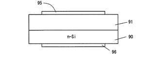
図7に示すように、n伝導型シリコン基板90上に、実施例1と同様にn伝導型カーボンナノウォール91を形成した。次に、n伝導型カーボンナノウォール91の端面上に金をEB蒸着法により堆積し、第1電極95を形成した。また、n伝導型シリコン基板90の裏面に金をEB蒸着法により堆積し、第2電極96を形成した。このようにして、n伝導型カーボンナノウォール91と金から成る第1電極95との界面にショットキー障壁を形成した。このショットキー障壁により第1電極95を陽極、第2電極96を陰極とする光起電力素子を形成した。この光起電力素子の電圧−電流特性を測定した。その結果を図8の曲線Aに示す。
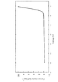
As shown in FIG. 7, an n-conducting
図8は、第1電極95の電位が第2電極96の電位よりも高くなる方向を電圧の正方向としている。第1電極95を正、第2電極96を負の電位とすると、電圧の増加に従って電流が指数関数的に増加することが観測された。一方、第2電極96を正、第1電極95を負の電位とすると、電圧を増加させても電流は、大きく増加しなかった。このように、本実施例の光起電力素子は、典型的な整流特性を示した。このことからショットキー障壁が存在することが理解され、これによりショットキー障壁を用いた光起電力素子が実現できる。
In FIG. 8, the direction in which the potential of the
なお、第1電極95を金に代えてアルミニウムにすると、電圧−電流特性は、図8の曲線Bに示すように、整流特性は見られなかった。すなわち、仕事関数の小さいアルミニウムの方が仕事関数の大きい金よりもオーミック性が良い。n型半導体に対しては、仕事関数が小さい金属の方がオーミック性が良いので、この図8の特性からもカーボンナノウォール91はn伝導型であることが分かる。
When the
〔比較例〕
実施例1において、窒素ラジカルを導入すくことなく、カーボンナノウォールをn型シリコン基板、p型シリコン基板に成長させた。この場合の電圧−電流特性を図9に示す。n型シリコン基板上にカーボンナノウォールを成長させた場合には、図9の曲線Aのような特性を示し、p型シリコン基板上にカーボンナノウォールを成長させた場合には、図9の曲線Bのような特性を示した。前者の抵抗率は、1.5×10⁴ Ω・cmであり、後者の抵抗率は4.1×10⁴ Ω・cmで、高抵抗率を示した。
[Comparative Example]
In Example 1, carbon nanowalls were grown on an n-type silicon substrate and a p-type silicon substrate without introducing nitrogen radicals. FIG. 9 shows the voltage-current characteristics in this case. When carbon nanowalls are grown on an n-type silicon substrate, the characteristics as shown by curve A in FIG. 9 are exhibited, and when carbon nanowalls are grown on a p-type silicon substrate, curves shown in FIG. B-like characteristics were exhibited. The former resistivity was 1.5 × 10 4 Ω · cm, and the latter resistivity was 4.1 × 10 4 Ω · cm, indicating a high resistivity.
光起電力素子は、図10の(a)に示すように、n−シリコン基板100の表面にアクセプタをドープしてp型領域102を形成し、そのp型領域102の上に、n導電型カーボンナノウォール105を形成して、光起電力素子を形成しても良い。この場合には、第1電極103がn導電型カーボンナノウォール105の上端面に形成され、第2電極104はp型領域102に形成される。
In the photovoltaic device, as shown in FIG. 10A, the surface of the n-
また、光起電力素子は、図10の(b)に示すように、n−シリコン基板100の上の酸化シリコン膜111の上に金属配線層112を形成し、その上に実施例2の構造のn導電型カーボンナノウォールと、その表面層に形成されたp伝導型カーボンナノウォールとの接合による光起電力素子115を形成しても良い。そして、p伝導型カーボンナノウォールの上に第1電極113を形成し、金属配線層112の上に第2電極114を形成しても良い。また、図10の(a)、(b)に示すように、シリコン基板110にトランジスタTrを形成して、本実施例の光起電力素子と共に集積回路を構成することができる。
Further, in the photovoltaic element, as shown in FIG. 10B, the
上記実施例では、カーボンナノウォールを用いた光起電力素子について説明したが、カーボンナノチューブを用いても同様に光起電力素子を構成できると考えられる。カーボンナノウォールなどのカーボンナノ構造体をn伝導型にするのにN原子を用いたが、他のP、As、Sb、BiなどのV族元素、O,S,SeなどのVI族元素を用いることができる。また、p伝導型とするには、Fを用いたが、他のハロゲン原子、B、Al、Ga、In、TlなどのIII 族元素、Be,Mg,Ca,Sr,BaなどのII族元素を用いることができる。製造には、これらの元素を含む有機金属ガスを用いたプラズマCVDが用いられる。 In the above embodiment, the photovoltaic device using the carbon nanowall has been described. However, it is considered that the photovoltaic device can be configured similarly even if the carbon nanotube is used. N atoms were used to make carbon nanostructures such as carbon nanowalls n-type, but other group V elements such as P, As, Sb and Bi, and group VI elements such as O, S and Se were used. Can be used. Also, F was used for the p-conductivity type, but other halogen atoms, group III elements such as B, Al, Ga, In, and Tl, group II elements such as Be, Mg, Ca, Sr, and Ba Can be used. For the production, plasma CVD using an organometallic gas containing these elements is used.
本発明は、新規な構造の光起電力素子である。太陽電池や電子回路に用いることができる。 The present invention is a photovoltaic device having a novel structure. It can be used for solar cells and electronic circuits.
2…カーボンナノウォール製造装置
70…p伝導型シリコン基板
80…n伝導型シリコン基板
73,81,91…n伝導型カーボンナノウォール
82…p伝導型カーボンナノウォール
10…反応室
14…ラジカル導入口
20…プラズマ放電手段
75,85,95…第1電極
76,86,96…第2電極
DESCRIPTION OF
Claims (8)
前記n伝導型カーボンナノウォールの上端面に接続する第1電極と、
前記p伝導型半導体に接続する第2電極と
を有することを特徴とする光起電力素子。 a p-conduction type semiconductor, and an n-conduction type carbon nanowall having a wall made of a single layer or multiple layers of a graphene sheet standing on the p-conduction type semiconductor,
A first electrode connected to an upper end surface of the n-conducting carbon nanowall;
And a second electrode connected to the p-conduction type semiconductor.
前記基板上に立設されたグラフェンシートの単層又は多重層から成る壁を有したn伝導型カーボンナノウォールと、
前記n伝導型カーボンナノウォールのグラフェンシートから成るそれぞれの壁面の表面に沿って壁面を覆うように形成された、グラフェンシートの単層又は多重層から成る壁を有したp伝導型カーボンナノウォールと
を有する光起電力素子。 A substrate,
An n-conducting carbon nanowall having a wall composed of a single layer or multiple layers of a graphene sheet erected on the substrate;
A p-conduction type carbon nanowall having a wall made of a single layer or multiple layers of a graphene sheet formed so as to cover the wall surface along the surface of each wall surface made of the graphene sheet of the n-conduction type carbon nanowall; A photovoltaic device having:
前記n伝導型カーボンナノウォールに接続する第2電極と
を有することを特徴とする請求項2に記載の光起電力素子。 A first electrode connected to an upper end surface of the p-conduction type carbon nanowall;
The photovoltaic device according to claim 2, further comprising: a second electrode connected to the n-conducting carbon nanowall.
前記導電性領域上に立設されたグラフェンシートの単層又は多重層から成る壁を有したn伝導型カーボンナノウォールと、
前記n伝導型カーボンナノウォールの上端面に形成された第1電極と、
前記導電性領域に接続する第2電極と
を有する光起電力素子。 A conductive region;
An n-conducting carbon nanowall having a wall composed of a single layer or multiple layers of a graphene sheet erected on the conductive region;
A first electrode formed on an upper end surface of the n-conducting carbon nanowall;
A photovoltaic device comprising: a second electrode connected to the conductive region.
Priority Applications (3)
| Application Number | Priority Date | Filing Date | Title |
|---|---|---|---|
| JP2005285668A JP5242009B2 (en) | 2005-09-29 | 2005-09-29 | Photovoltaic device using carbon nanowall |
| US11/992,751 US20100212728A1 (en) | 2005-09-29 | 2006-09-28 | Diode and Photovoltaic Device Using Carbon Nanostructure |
| PCT/JP2006/319368 WO2007037343A1 (en) | 2005-09-29 | 2006-09-28 | Diode and photovoltaic element using carbon nanostructure |
Applications Claiming Priority (1)
| Application Number | Priority Date | Filing Date | Title |
|---|---|---|---|
| JP2005285668A JP5242009B2 (en) | 2005-09-29 | 2005-09-29 | Photovoltaic device using carbon nanowall |
Publications (2)
| Publication Number | Publication Date |
|---|---|
| JP2007096136A JP2007096136A (en) | 2007-04-12 |
| JP5242009B2 true JP5242009B2 (en) | 2013-07-24 |
Family
ID=37981450
Family Applications (1)
| Application Number | Title | Priority Date | Filing Date |
|---|---|---|---|
| JP2005285668A Active JP5242009B2 (en) | 2005-09-29 | 2005-09-29 | Photovoltaic device using carbon nanowall |
Country Status (1)
| Country | Link |
|---|---|
| JP (1) | JP5242009B2 (en) |
Families Citing this family (20)
| Publication number | Priority date | Publication date | Assignee | Title |
|---|---|---|---|---|
| US7858876B2 (en) * | 2007-03-13 | 2010-12-28 | Wisconsin Alumni Research Foundation | Graphite-based photovoltaic cells |
| KR101368808B1 (en) * | 2007-07-05 | 2014-03-03 | 주성엔지니어링(주) | Crystalline silicon solar cell comprising CNT layer and manufacturing method thereof |
| CN101552295A (en) | 2008-04-03 | 2009-10-07 | 清华大学 | Solar cell |
| CN101527327B (en) | 2008-03-07 | 2012-09-19 | 清华大学 | Solar cell |
| JP2011129541A (en) * | 2008-03-07 | 2011-06-30 | Tohoku Univ | Solar cell |
| CN101552296B (en) * | 2008-04-03 | 2011-06-08 | 清华大学 | Solar cell |
| US20110000533A1 (en) * | 2008-03-07 | 2011-01-06 | National University Corporation Tohoku University | Photoelectric conversion element structure and solar cell |
| CN101562204B (en) | 2008-04-18 | 2011-03-23 | 鸿富锦精密工业(深圳)有限公司 | Solar energy battery |
| KR100953448B1 (en) * | 2008-04-02 | 2010-04-20 | 한국기계연구원 | Photoelectric conversion device using semiconductor nano material and method for manufacturing thereof |
| KR20110102322A (en) | 2008-12-10 | 2011-09-16 | 가부시키가이샤 시나노 | Thin-film photoelectric transducer and method for manufacturing thin-film photoelectric transducer |
| CN102414840A (en) | 2009-04-30 | 2012-04-11 | 汉阳大学校产学协力团 | Silicon solar cell comprising a carbon nanotube layer |
| JP5582744B2 (en) * | 2009-08-20 | 2014-09-03 | 日立造船株式会社 | SOLAR CELL, ITS MANUFACTURING METHOD, AND SOLAR CELL DEVICE |
| JP5393345B2 (en) * | 2009-08-25 | 2014-01-22 | 日立造船株式会社 | Solar cell and solar cell device |
| JP5383443B2 (en) * | 2009-11-16 | 2014-01-08 | 日立造船株式会社 | SOLAR CELL, ITS MANUFACTURING METHOD, AND SOLAR CELL DEVICE |
| WO2011058544A2 (en) * | 2009-11-16 | 2011-05-19 | Nextpv Inc. | Graphene-based photovoltaic device |
| WO2011152459A1 (en) * | 2010-06-03 | 2011-12-08 | 株式会社Si-Nano | Optical electricity storage device |
| EP2523226A4 (en) * | 2010-06-10 | 2014-04-09 | Nusola Inc | Light power generation device |
| JP2013159521A (en) * | 2012-02-03 | 2013-08-19 | Chube Univ | Method for producing graphene film |
| JP6210445B2 (en) * | 2012-07-04 | 2017-10-11 | 国立大学法人名古屋大学 | Method for producing carbon nanotube |
| KR20150113164A (en) * | 2013-02-07 | 2015-10-07 | 가부시키가이샤 아이에이치아이 | Oxygen reduction catalyst, oxygen reduction electrode, and fuel cell |
Family Cites Families (7)
| Publication number | Priority date | Publication date | Assignee | Title |
|---|---|---|---|---|
| JPH05335614A (en) * | 1992-06-03 | 1993-12-17 | Idemitsu Kosan Co Ltd | Photoelectric conversion element |
| JP3249619B2 (en) * | 1993-02-15 | 2002-01-21 | 大阪瓦斯株式会社 | Solar cell |
| JP2546511B2 (en) * | 1993-08-26 | 1996-10-23 | 日本電気株式会社 | Method for synthesizing fullerene and carbon nanotube |
| JP2003016954A (en) * | 2001-04-25 | 2003-01-17 | Sony Corp | Electron emission device and its manufacturing method, cold cathode field electron emission element and its manufacturing method, and cold cathode field electron emission display device and its manufacturing method |
| JP2003209270A (en) * | 2002-01-15 | 2003-07-25 | Toyota Central Res & Dev Lab Inc | Carbon photoelectric element and its manufacturing method |
| JP4514402B2 (en) * | 2002-10-28 | 2010-07-28 | シャープ株式会社 | Semiconductor device and manufacturing method thereof |
| US20070184190A1 (en) * | 2003-08-27 | 2007-08-09 | Mineo Hiramatsu | Method for producing carbon nanowalls, carbon nanowall, and apparatus for producing carbon nanowalls |
-
2005
- 2005-09-29 JP JP2005285668A patent/JP5242009B2/en active Active
Also Published As
| Publication number | Publication date |
|---|---|
| JP2007096136A (en) | 2007-04-12 |
Similar Documents
| Publication | Publication Date | Title |
|---|---|---|
| JP5242009B2 (en) | Photovoltaic device using carbon nanowall | |
| US20100212728A1 (en) | Diode and Photovoltaic Device Using Carbon Nanostructure | |
| JP5054896B2 (en) | Carbon nanowall processing method, carbon nanowall, carbon nanowall device | |
| JP5116961B2 (en) | Diode using carbon nanowall | |
| KR101993382B1 (en) | Graphene on substrate and process for preparing the same | |
| KR101878734B1 (en) | Layered structure of graphene, process for preparing the same, and transparent electrode and transistor comprising the structure | |
| CN1957116B (en) | Nanocrystal diamond film, process for producing the same and apparatus using nanocrystal diamond film | |
| TW562868B (en) | Plasma deposition device for forming thin film | |
| JP5578548B2 (en) | Method for selective growth and formation of carbon nanowall | |
| US20090258255A1 (en) | Method for Producing Diamond Having Acicular Projection Array Structure on Surface thereof, Diamond Material, Electrode and Electronic Device | |
| US7589002B2 (en) | Method of forming an oxygen- or nitrogen-terminated silicon nanocrystalline structure and an oxygen- or nitrogen-terminated silicon nanocrystalline structure formed by the method | |
| JPWO2005021430A1 (en) | Carbon nanowall manufacturing method, carbon nanowall and manufacturing apparatus | |
| JP4766895B2 (en) | Carbon nanowall device | |
| JPH02239623A (en) | Stabilizing layer and its manufacture | |
| JPH09142821A (en) | Accumulation of amorphous silicon-based film | |
| Cui et al. | Study of direct tunneling and dielectric breakdown in molecular beam epitaxial hexagonal boron nitride monolayers using metal–insulator–metal devices | |
| JP4762945B2 (en) | Carbon nanowall structure | |
| RU2391738C2 (en) | Structure and method for manufacturing of field emission elements with carbon nanotubes used as cathodes | |
| JP4975289B2 (en) | Electronic devices using carbon nanowalls | |
| JP5053595B2 (en) | DLC film forming method and DLC film manufacturing apparatus | |
| JP5028593B2 (en) | Method for producing transparent conductive film | |
| Choi et al. | Field-emission characteristics of nitrogen-doped diamond-like carbon film deposited by filtered cathodic vacuum arc technique | |
| JP5888685B2 (en) | Electronic devices using carbon nanowalls | |
| JP2002352694A (en) | Electrode, electron emission element and device using it | |
| JP4312331B2 (en) | Electron emission device |
Legal Events
| Date | Code | Title | Description |
|---|---|---|---|
| A621 | Written request for application examination |
Free format text: JAPANESE INTERMEDIATE CODE: A621 Effective date: 20080812 |
|
| A131 | Notification of reasons for refusal |
Free format text: JAPANESE INTERMEDIATE CODE: A131 Effective date: 20120124 |
|
| A521 | Request for written amendment filed |
Free format text: JAPANESE INTERMEDIATE CODE: A523 Effective date: 20120323 |
|
| A131 | Notification of reasons for refusal |
Free format text: JAPANESE INTERMEDIATE CODE: A131 Effective date: 20121127 |
|
| A521 | Request for written amendment filed |
Free format text: JAPANESE INTERMEDIATE CODE: A523 Effective date: 20130128 |
|
| TRDD | Decision of grant or rejection written | ||
| A01 | Written decision to grant a patent or to grant a registration (utility model) |
Free format text: JAPANESE INTERMEDIATE CODE: A01 Effective date: 20130402 |
|
| A61 | First payment of annual fees (during grant procedure) |
Free format text: JAPANESE INTERMEDIATE CODE: A61 Effective date: 20130403 |
|
| FPAY | Renewal fee payment (event date is renewal date of database) |
Free format text: PAYMENT UNTIL: 20160412 Year of fee payment: 3 |
|
| R150 | Certificate of patent or registration of utility model |
Free format text: JAPANESE INTERMEDIATE CODE: R150 Ref document number: 5242009 Country of ref document: JP Free format text: JAPANESE INTERMEDIATE CODE: R150 |
|
| R250 | Receipt of annual fees |
Free format text: JAPANESE INTERMEDIATE CODE: R250 |
|
| R250 | Receipt of annual fees |
Free format text: JAPANESE INTERMEDIATE CODE: R250 |
|
| S111 | Request for change of ownership or part of ownership |
Free format text: JAPANESE INTERMEDIATE CODE: R313115 |
|
| S111 | Request for change of ownership or part of ownership |
Free format text: JAPANESE INTERMEDIATE CODE: R313117 |
|
| R350 | Written notification of registration of transfer |
Free format text: JAPANESE INTERMEDIATE CODE: R350 |
|
| R350 | Written notification of registration of transfer |
Free format text: JAPANESE INTERMEDIATE CODE: R350 |
|
| S533 | Written request for registration of change of name |
Free format text: JAPANESE INTERMEDIATE CODE: R313533 |
|
| R350 | Written notification of registration of transfer |
Free format text: JAPANESE INTERMEDIATE CODE: R350 |