JP4503809B2 - Semiconductor memory device - Google Patents
Semiconductor memory device Download PDFInfo
- Publication number
- JP4503809B2 JP4503809B2 JP2000333719A JP2000333719A JP4503809B2 JP 4503809 B2 JP4503809 B2 JP 4503809B2 JP 2000333719 A JP2000333719 A JP 2000333719A JP 2000333719 A JP2000333719 A JP 2000333719A JP 4503809 B2 JP4503809 B2 JP 4503809B2
- Authority
- JP
- Japan
- Prior art keywords
- word line
- voltage
- memory cell
- transfer
- transfer transistor
- Prior art date
- Legal status (The legal status is an assumption and is not a legal conclusion. Google has not performed a legal analysis and makes no representation as to the accuracy of the status listed.)
- Expired - Fee Related
Links
Images


Classifications
-
- G—PHYSICS
- G11—INFORMATION STORAGE
- G11C—STATIC STORES
- G11C8/00—Arrangements for selecting an address in a digital store
- G11C8/10—Decoders
-
- G—PHYSICS
- G11—INFORMATION STORAGE
- G11C—STATIC STORES
- G11C16/00—Erasable programmable read-only memories
- G11C16/02—Erasable programmable read-only memories electrically programmable
- G11C16/04—Erasable programmable read-only memories electrically programmable using variable threshold transistors, e.g. FAMOS
- G11C16/0483—Erasable programmable read-only memories electrically programmable using variable threshold transistors, e.g. FAMOS comprising cells having several storage transistors connected in series
-
- G—PHYSICS
- G11—INFORMATION STORAGE
- G11C—STATIC STORES
- G11C16/00—Erasable programmable read-only memories
- G11C16/02—Erasable programmable read-only memories electrically programmable
- G11C16/06—Auxiliary circuits, e.g. for writing into memory
- G11C16/08—Address circuits; Decoders; Word-line control circuits
-
- G—PHYSICS
- G11—INFORMATION STORAGE
- G11C—STATIC STORES
- G11C8/00—Arrangements for selecting an address in a digital store
- G11C8/08—Word line control circuits, e.g. drivers, boosters, pull-up circuits, pull-down circuits, precharging circuits, for word lines
Description
【0001】
【発明の属する技術分野】
この発明は、半導体記憶装置に関し、特にロウデコーダ内の転送トランジスタの配置に係り、NAND型フラッシュメモリ等の不揮発性メモリに使用されるものである。
【0002】
【従来の技術】
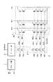
図7は、従来の半導体記憶装置について説明するためのもので、NAND型フラッシュメモリにおけるロウデコーダとメモリセルアレイの一部を抽出して示している。ロウアドレス、あるいはロウアドレスのプリデコード信号A0,A1,…,Amは、デコード部1に供給されてデコードされ、このデコード部1によりメモリセルアレイ中の1つのNANDセルブロック4が選択される。上記デコード部1から出力されるデコード信号は、ブースター部2に供給される。このブースター部2は、選択されたブロック4内にのみ、ワード線のアドレスに対応したワード線駆動信号CG0〜CGi及び選択ゲート駆動信号SG1,SG2を供給するために、転送トランジスタ3のゲート5を制御している。ブロック4が選択状態の時、ブースター部2はデコード部1から出力されるデコード信号により、転送トランジスタ3のゲート5に所定の電圧を印加してオン状態にし、ブロック4が非選択状態の時は、転送トランジスタ3のゲート5を接地レベルとしてオフ状態にする。
【0003】
NAND型メモリにおける1つのNANDセル4aは、ゲートが選択ゲート線SGS,SGDに接続された2つの選択トランジスタS1,S2と、これら選択トランジスタS1,S2間に電流通路が直列接続され、ゲートがそれぞれワード線WL0〜WLiに接続されたメモリセルMC0〜MCiとから構成されている。上記選択トランジスタS1の電流通路の一端は、ソース線CELSRCに接続され、上記選択トランジスタS2の電流通路の一端は、ビット線BL0〜BLjに接続される。
【0004】
そして、ロウアドレス、あるいはロウアドレスのプリデコード信号A0,A1,…,AmによりNANDセルブロック4が選択され、更にNANDセル4a内のワード線のアドレスが選択されると、個々のメモリセルMC0〜MCiにアクセスすることができる。
【0005】
図8は、上記NAND型フラッシュメモリの書き込み時における各信号の波形図を示している。また、図9(a),(b)はそれぞれ、上記NANDセル4aの断面構成と、書き込み時のNANDセル4a内のバイアス条件を示しており、(a)図は“0”の書き込み(Program)時、(b)図は“1”の書き込み時である。図9(a),(b)では、メモリセル12が選択セルとなっており、ワード線WL2が選択ワード線(WL)となる。その他のメモリセルは全て非選択セルとなるが、図8におけるワード線WL1とWL3は隣接非選択ワード線(WL)、その他が非選択ワード線(WL)となる。また、この図8に示す書き込み方式においては、書き込みを行う前は、NAND内セル4aは消去状態(メモリセルのしきい値電圧が負)となっている。
【0006】
メモリセルにデータ書き込む場合には、まず、ビット線BLに書き込みデータを転送する。NAND型フラッシュメモリでは、1本のワード線で選択されるメモリセルに対し、一括に書き込み動作を行うことにより、書き込み速度を高速化しており、同時に書き込む単位、例えば512バイト分のデータラッチを有している。これらのデータラッチから、“1”書き込みセルには、ビット線にVddが転送され、“0”書き込みのセルにはビット線に0Vが転送される。また、書き込みを行うワード線を有する選択ブロックにおいては、ロウデコーダ用駆動電圧VRDECが印加されると、転送トランジスタ3のゲート5にもこのロウデコーダ用駆動電圧VRDEC以上の電圧、例えば22Vが印加される。
【0007】
これにより、選択NANDセルにおいては、選択トランジスタ15のゲートにVddが印加され、NANDセル4a内のチャネルがビット線BLからプリチャージされる。
【0008】
次に、非選択ワード線に10V程度のVPASS電位を印加する。
【0009】
図9(a)に示すように、“0”書き込みでは、選択メモリセル12から選択トランジスタ15までのメモリセル13,14,…は、しきい値電圧が負であるため導通しており、チャネル電位は0Vに保持される。一方、図9(b)に示すように、“1”書き込みでは、選択トランジスタ15は、ビット線BLがVdd、ゲートがVdd、NANDセル側のソースが「Vdd−Vt」に充電されてカットオフしているため、NANDセル内のチャネル電位は、非選択ワード線の電位の上昇に伴い、容量カップリングにより昇圧される。従って、チャネル電位Vch1及びVch3は、非選択ワード線の電位VPASSに応じた電位に持ち上げられる。この際、チャネル電位Vch2は、ワード線WL1,WL2,WL3が0Vであるため、それらによる電位の変化はないが、チャネル電位Vch1とVch3の上昇に伴い、メモリセル11と13のしきい値落ち電圧程度に充電されている。
【0010】
次に、選択ワード線WL2に、20V程度の書き込み電圧VPGMを印加する。
【0011】
図9(a)の“0”書き込みセルにおいては、メモリセル12のチャネルとビット線BLが0Vで導通した状態を保持するため、ワード線WL2とチャネル間に20Vの電位差がつき、浮遊ゲートにチャネルから電子が注入されて、しきい値電圧が高くなり書き込みが行われる。図9(b)の“1”書き込みセルにおいては、メモリセル12のチャネル電位がメモリセル11と13の負のしきい値落ちの電位に充電されたフローティングの状態から、ワード線WL2の昇圧により、より高い電位のフローティング状態に変化する。ワード線WL2の電位変化に伴って、メモリセル12のチャネル電位も高くなるため、チャネルから浮遊ゲートへの電子の注入はほとんど行われず、書き込み前の状態を保持する。
【0012】
このようにして、“0”書き込みと“1”書き込み(非書き込み)が行われる。よって、ロウデコーダは、これらのワード線電圧を選択的に転送する必要がある。
【0013】
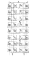
ここで、従来のロウデコーダにおける転送トランジスタ3部のレイアウトイメージを図10に示す。図面及び説明を簡略化するため、ここでは、転送トランジスタ3が8個の場合について示している。
【0014】
Yt,Yd間の距離は、NANDセル4aのサイズによって決まるサイズであり、図10では転送トランジスタ3を2段積みにして配置している。各転送トランジスタ3は、p型基板上に形成されたNMOSトランジスタとなっており、ソース・ドレイン領域は書き込み電圧及び消去電圧の印加に対して充分な耐圧を持つ構造になっている。
【0015】
上記図10に示したような転送トランジスタ3の配置において、前述の書き込み方式でのバイアス状態を図11に示す。図11においては、ワード線WL3が選択ワード線となっている。隣接非選択ワード線は、ワード線WL2とWL4である。
【0016】
この時、ワード線駆動信号CG2とCG3が供給される転送トランジスタ間との距離X1は、ソース・ドレイン領域間に20V、ゲートに20V以上の電圧が印加されたフィールドトランジスタにおいて、所定のリーク電流以下の条件を満たす大きさとしなければならない。また、ワード線駆動信号CG3とCG4が供給される転送トランジスタ間の距離Y1は、p型基板上の素子分離領域を挟んだ、n型拡散層領域間に20Vが印加されたときに、所定のリーク電流以下の条件を満たす大きさとしなければならない。上記距離X1については、転送トランジスタ3のゲート5がp型素子分離領域上でフィールドトランジスタのゲートとなっているが、ゲート5を各転送トランジスタ3間で分離して描いても良く、その場合は、Y1の条件に近づく。
【0017】
この場合、距離YBが大きく、距離Y1を充分離した上で図11のような配置ができる場合は良いが、距離X1が大きい場合には、ロウデコーダの横幅が大きくなる。また、メモリセルの微細化により、距離YBが著しく小さくなると、図11のような2段積では描けなくなり、転送トランジスタ3を横並びにする数が増えて、ロウデコーダの横幅が顕著に大きくなる可能性がある。
【0018】
【発明が解決しようとする課題】
上記のように従来の半導体記憶装置では、メモリセルの制御ゲートに書き込み電圧や消去電圧を印加するロウデコーダ内の転送トランジスタには、書き込み、消去電圧に対して充分な耐圧を有するサイズの大きなものが必要となる。また、大きな素子分離領域も必要になり、この結果ロウデコーダのパターン占有面積が大きくなるという問題があった。
【0019】
この発明は上記のような事情に鑑みてなされたもので、その目的とするところは、転送トランジスタを適切な配置にすることによって、転送トランジスタ間の距離を無駄に広げる必要がなくなり、ロウデコーダのパターン占有面積を小さくできる半導体記憶装置を提供することにある。
【0020】
【課題を解決するための手段】
この発明の一態様に係る半導体記憶装置は、電気的に書き換え可能な不揮発性メモリセルが配列されたメモリセルアレイと、前記メモリセルアレイにおける複数のワード線を有するブロックを選択する選択手段と、前記ブロック内の複数のワード線への印加電圧が入力される複数のワード線駆動信号線と、前記ワード線駆動信号線とメモリセル内ワード線との間に接続され、前記選択手段の出力により制御される複数の転送トランジスタが行及び列に配置され、前記メモリセルアレイから少なくとも1つのメモリセルの行を選択するように構成されたワード線選択回路とを具備し、書き込み動作において、第1の電圧と、第1の電圧より高い第2の電圧と、第2の電圧より高い第3の電圧が、選択されたブロック内の複数のワード線に対して同時に印加される状態を有し、前記ワード線選択回路は、前記第1の電圧が印加される第1の転送トランジスタと、前記第2の電圧が印加される第2の転送トランジスタと、前記第3の電圧が印加される第3の転送トランジスタを有し、前記第3の転送トランジスタと前記第1の転送トランジスタが隣接することがないように、特定の転送トランジスタに接続されたワード線と、それと隣接する転送トランジスタに接続されたワード線のアドレスが連続しないように前記第1乃至第3の転送トランジスタが上下左右に配置されており、前記ブロック内の複数の転送トランジスタにおける、転送トランジスタのワード線側端子が向き合って配置される側の第1の素子分離領域幅は、転送トランジスタのワード線駆動信号線側端子と他の転送トランジスタのワード線側端子が向き合って配置される側の第2の素子分離領域幅よりも小さい。
【0021】
上記半導体記憶装置において、隣接して配置される転送トランジスタに接続されるワード線のアドレスが2以上離れている。
【0023】
上記半導体記憶装置において、前記第1の電圧は隣接非選択ワード線に印加する電圧であり、前記第3の電圧は選択ワード線に印加する書き込み電圧であり、前記第2の電圧は非選択ワード線に印加する中間電圧である。
【0024】
上記半導体記憶装置において、前記ブロック内の複数の転送トランジスタのワード線側端子からそれぞれのワード線への引き出し配線は、メモリセルアレイ中のワード線と同じ並びとなるように引き出される。
【0025】
上記半導体記憶装置において、前記ブロック内の複数の転送トランジスタのワード線側端子からそれぞれのワード線への引き出し配線は、ワード線を形成する配線より1つ上層の金属配線である。
【0026】
上記半導体記憶装置において、前記メモリセルアレイのロウアドレス、あるいはロウアドレスのプリデコード信号をデコードするデコード部と、上記デコード部から出力されるデコード信号が供給されるブースター部とを更に具備し、前記転送トランジスタは上記ブースター部の出力信号でオン/オフ制御され、メモリセルアレイ中の選択されたブロックに選択信号を供給する。
【0027】
上記半導体記憶装置において、前記メモリセルアレイは、複数のブロックに分割され、前記ブロックの各々は、各々のゲートが前記転送トランジスタの電流通路の一端に接続された第1,第2の選択トランジスタと、前記第1,第2の選択トランジスタ間に電流通路が直列接続され、ゲートが前記転送トランジスタの電流通路の一端にそれぞれ接続されたメモリセルとを備える。
【0028】
上記のような構成によれば、ロウデコーダの同一ブロック内の転送トランジスタ間に印加される電位差を小さくすることができ、素子分離領域を小さくすることができる。この結果、ロウデコーダのパターン占有面積を小さくできる。
【0029】
同一ブロック内の転送トランジスタ間に印加される電位差を小さくするには、隣接して配置される2つの転送トランジスタのワード線のアドレスが2個以上離れていれば良い。
【0030】
転送トランジスタ間に印加される電位差が小さいところは素子分離領域を小さくし、電位差が大きいところは素子分離領域を大きくすることにより、無駄に素子分離領域を大きくすることなく、最適なロウデコーダのサイズにすることができる。
【0031】
また、上記のような構成によれば、ロウデコーダの同一ブロック内の転送トランジスタが3段積み以上の配置となった場合に、転送トランジスタ間に印加される電位差が小さいところは素子分離領域を小さくし、電位差が大きいところは素子分離領域を大きくすることにより、無駄に素子分離領域を大きくすることなく、最適なロウデコーダのサイズにすることができる。しかも、転送トランジスタのワード線側端子とワード線駆動信号端子が向き合う素子分離領域において大きな電位差が生ずる場合があり、この素子分離領域を大きくすることは避けられないが、それ以外の部分においては、転送トランジスタの素子分離領域に印加される電位差を小さくするようにアドレスを割り付けることによって、最適なロウデコーダのサイズにできる。
【0032】
引き出し配線の並びと、メモリセルアレイ中のワード線の並びを同じにすることにより、ルールが最も厳しいワード線と引き出し配線の接続を容易にすることができる。
【0033】
引き出し配線を、ワード線を形成する配線より1つ上層の金属配線のみでレイアウトすることにより、金属配線のつなぎ替えをなくし、ワード線への不要なプロセスダメージを軽減することができる。
【0034】
上記のような構成によれば、転送トランジスタのワード線側端子から、ワード線に至るまでの引き出し配線を、ワード線を形成する配線より1つ上層の金属配線のみでレイアウトするので、金属配線のつなぎ替えをなくすことができ、ワード線、すなわち不揮発性メモリの制御ゲートへの不要なプロセスダメージを軽減することができる。
【0035】
メモリセルアレイとしては、第1,第2の選択トランジスタと、前記第1,第2の選択トランジスタ間に電流通路が直列接続され、ゲートが前記転送トランジスタの電流通路の一端にそれぞれ接続されたメモリセルとを備える構造が適用できる。
【0036】
【発明の実施の形態】
以下、この発明の実施の形態について図面を参照して説明する。
[第1の実施の形態]
図1は、この発明の第1の実施の形態に係る半導体記憶装置について説明するためのもので、本実施の形態における転送トランジスタの配置を示すパターン平面図である。図1では、図10に示した従来の配置例に対して、転送トランジスタ3のワード線のアドレスに対する割付を変更しており、上下左右の転送トランジスタ3におけるワード線のアドレスを連続しない割付にすることによって、図2に示すように20Vの大きな電位差がかかる場所をなくしている。
【0037】
すなわち、図2の転送トランジスタの下段の並びを、CG1(WL1),CG3(WL3),CG0(WL0),CG2(WL2)とすることで、X方向の転送トランジスタ間で、どのワード線が選択された場合にも、10Vの電位差で済むようにしている。また、上段の並びをCG5(WL5),CG7(WL7),CG4(WL4),CG6(WL6)とすることにより、同様にそれらのX方向の転送トランジスタ間の電位差が10Vに抑えられるとともに、Y方向のトランジスタ間においても、Y2,Y3部位に示すように10Vの電位差で抑えるようにしている。
【0038】
従って、図8及び図9(a),(b)に示したような書き込み方式を行う場合において、ロウデコーダにおける転送トランジスタ周りのサイズ、例えば素子分離領域の幅を10V以上の耐圧を持つように設計すれば良く、従来に比して狭くすることができる。
【0039】
なお、転送トランジスタ3のワード線のアドレスの割付は、図1及び図2は一例であり、上下、左右の転送トランジスタ3のアドレスが連続しなければ、異なる割り付け方でも構わない。
【0040】
特に、実際のレイアウトにおいては、各転送トランジスタ3のワード線側端子からワード線に引き出す配線のルールにより、図1のような割り付けができない場合があるので、配線の通し方を考えてアドレス割り付けを適宜最適化することになる。
【0041】
図1は、転送トランジスタ3の各ワード線側端子から、タングステン配線により、メモリセル側へ配線が引き出されるパターンをイメージしたものである。図1に示すように、ワード線のアドレスと同一の並びになるようにタングステン配線で引き出された先でメモリセルアレイ中のワード線を形成するポリシリコン配線あるいはポリサイド配線に接続される。メモリセルアレイ中のワード線ピッチは、最もルールが微細化されているため、転送ゲートからの引き出し配線とワード線の配線との接続を容易にするためには、並びを一致させる必要がある。また、この引き出し配線は、メモリセルの制御ゲートであるワード線配線層(この場合、ポリシリコン配線あるいはポリサイド配線)にできるだけ近い金属配線層のみでワード線に引き出すことが望ましい。なぜなら、他の金属配線へのつなぎ替えが増えると、不揮発性メモリの制御ゲートであるワード線がフローティングのまま、ヴィアコンタクトプロセスを経過することになり、メモリセルへ不要なプロセスダメージを与える可能性があるからである。よって、複数の転送トランジスタからワード線への引き出し配線が交差することなく、例えば図1に示すような引き出し方法で、前述のアドレス割り付けを実現するのが望ましい。
【0042】
上述したように、転送トランジスタを適切な配置にすることによって、転送トランジスタ間の距離を無駄に広げる必要がなくなり、ロウデコーダのパターン占有面積を小さくできる。
【0043】
[第2の実施の形態]
図3は、この発明の第2の実施の形態に係る半導体記憶装置について説明するためのもので、16個のメモリセルが直列接続されたNANDセルに対する転送トランジスタの配置例を示している。図3の配置から明らかなように、図1及び図2と同様にアドレスの割り付けが上下左右で連続していない。しかも、この第2の実施の形態では、上下、左右だけでなく、上下の斜め方向も含めてワード線のアドレスが連続しないアドレスの割り付けとなっている。
【0044】
従って、本第2の実施の形態によれば、16個のメモリセルが直列接続されたNANDセルであっても転送トランジスタを適切な配置にでき、転送トランジスタ間の距離を無駄に広げる必要がなくなり、ロウデコーダのパターン占有面積を小さくできる。
【0045】
[第3の実施の形態]
図4は、この発明の第3の実施の形態に係る半導体記憶装置について説明するためのもので、1つのNANDセルに対応する転送トランジスタが3段に積まれる場合の配置例を示している。NAND型メモリセルは、前述のように直列に接続されるメモリセルと2つの選択トランジスタにより構成されており、2つの選択トランジスタが1つのメモリセルに対するオーバーヘッドとなっている。よって、セルアレイを小さくするには、選択トランジスタが含まれる割合をメモリセル8個に1個、メモリセル16個に1個と減らすことが1つの有効な手段となる。
【0046】
しかし、メモリセルの直列接続数が増えた場合には、距離YBも大きくなるので、Y方向に積む転送トランジスタの数を増やして、ロウデコーダのX方向の幅を小さくすることが必要となる。この場合、図1乃至図3と異なり、転送トランジスタのCG0,CG1,CGi端子と、他の転送トランジスタのワード線側端子が向き合う部位ができる。
【0047】
図1乃至図3では、上段と下段で転送トランジスタのワード線側端子が向き合い、YtとYdでは折り返しパターンとなっていた。
【0048】
この場合、図5に示す非選択ブロックの消去状態において、中段のCG0,CG1〜CGi端子は0V、上段のワード線側端子は20Vというバイアス状態が存在する。
【0049】
なぜなら、消去時には、選択ブロックのワード線を0Vにするため、CG0,CG1〜CGiには、全て0Vが印加される。非選択ブロックにおいては、転送トランジスタ3のゲート5が接地されているため、ワード線側ノードはフローティングになる。消去時のバイアス状態は、セルpウェルに20Vが印加され、選択ブロックにおいては、全ワード線が0Vになり、メモリセルの制御ゲートとセルpウェル間に20Vが印加されることにより、浮遊ゲートから電子が放出される(図6(a)参照)。
【0050】
なお、図6(a)は消去時、図6(b)は書き込み時の動作を模式的に示す断面図であり、510は制御ゲート(ワード線)、511は浮遊ゲート、512はソース・ドレイン領域、513はセルpウェルである。また、図6(c)は書き込み前と書き込み後のメモリセルのしきい値分布を示している。
【0051】
一方、非選択ブロックにおいては、ワード線がフローティングになるため、セルpウェルに20Vが印加されると、容量カップリングによりフローティングのワード線電位が同時に持ち上がるため、メモリセルの制御ゲートとセルpウェル間に消去に充分な電位差がつかず、消去されない。
【0052】
従って、図5の非選択ブロックにおいては、中段と上段との間で、転送トランジスタ間に20V近い電位差が生ずる。このような場合には、この距離Y4は大きくする必要があるので、下段と中段の間の素子分離領域の距離Y2またはY3よりY4を大きくする。逆に距離Y4とY2またはY3の素子分離領域を個別に最適化したサイズにすることによって、転送トランジスタ領域のサイズを小さくすることができる。
【0053】
以上第1乃至第3の実施の形態を用いてこの発明の説明を行ったが、この発明は上記各実施の形態に限定されるものではなく、実施段階ではその要旨を逸脱しない範囲で種々に変形することが可能である。また、上記各実施の形態には種々の段階の発明が含まれており、開示される複数の構成要件の適宜な組み合わせにより種々の発明が抽出され得る。例えば各実施の形態に示される全構成要件からいくつかの構成要件が削除されても、発明が解決しようとする課題の欄で述べた課題の少なくとも1つが解決でき、発明の効果の欄で述べられている効果の少なくとも1つが得られる場合には、この構成要件が削除された構成が発明として抽出され得る。
【0054】
【発明の効果】
以上説明したように、この発明によれば、転送トランジスタを適切な配置にすることによって、転送トランジスタ間の距離を無駄に広げる必要がなくなり、ロウデコーダのパターン占有面積を小さくできる半導体記憶装置が得られる。
【図面の簡単な説明】
【図1】この発明の第1の実施の形態に係る半導体記憶装置について説明するためのもので、本実施の形態における転送トランジスタの配置を示すパターン平面図。
【図2】図1に示した転送トランジスタの配置における転送トランジスタ間の電位差について説明するためのパターン平面図。
【図3】この発明の第2の実施の形態に係る半導体記憶装置について説明するためのもので、16個のメモリセルが直列接続されたNANDセルに対する転送トランジスタの配置例を示すパターン平面図。
【図4】この発明の第3の実施の形態に係る半導体記憶装置について説明するためのもので、1つのNANDセルに対応する転送トランジスタが3段に積まれる場合の例を示すパターン平面図。
【図5】図4に示した転送トランジスタの配置における非選択ブロックの消去動作時の状態において、転送トランジスタ間の電位差について説明するためのパターン平面図。
【図6】消去時と書き込み時の動作を模式的に示すための図。
【図7】従来の半導体記憶装置について説明するためのもので、NAND型フラッシュメモリにおけるロウデコーダとメモリセルアレイの一部を抽出して示す回路図。
【図8】NAND型フラッシュメモリの書き込み時における各信号の波形図。
【図9】NANDセルの断面構成と、書き込み時のNANDセル内のバイアス条件を示す図。
【図10】転送トランジスタを2段積みにして配置した場合のパターン平面図。
【図11】図10に示した書き込み方式でのバイアス状態を示すパターン平面図。
【符号の説明】
1…デコード部、
2…ブースター部、
3…転送トランジスタ、
4…NANDセルブロック、
4a…NANDセル、
5…転送トランジスタのゲート、
A0,A1,…,Am…ロウアドレス、あるいはロウアドレスのプリデコード信号、
S1,S2,16,15…選択トランジスタ、
SGS,SGD…選択ゲート線、
SG1,SG2…選択ゲート駆動信号、
CG0〜CGi…ワード線駆動信号、
WL0〜WLi…ワード線、
BL0〜BLj…ビット線、
CELSRC…ソース線、
MC0〜MCi,10〜15…メモリセル、
VRDEC…ロウデコーダ用駆動電圧。[0001]
BACKGROUND OF THE INVENTION
The present invention relates to a semiconductor memory device, and more particularly to an arrangement of transfer transistors in a row decoder, and is used for a nonvolatile memory such as a NAND flash memory.
[0002]
[Prior art]
FIG. 7 is a diagram for explaining a conventional semiconductor memory device, and shows a part of a row decoder and a memory cell array in a NAND flash memory. The row address or row address predecode signals A0, A1,..., Am are supplied to the
[0003]
One
[0004]
When the
[0005]
FIG. 8 shows a waveform diagram of each signal at the time of writing in the NAND flash memory. FIGS. 9A and 9B show the cross-sectional configuration of the
[0006]
When data is written to the memory cell, first, write data is transferred to the bit line BL. In the NAND flash memory, the write speed is increased by performing a batch write operation on the memory cells selected by one word line, and there is a data latch for 512 bytes at the same time, for example. is doing. From these data latches, Vdd is transferred to the bit line to the “1” write cell, and 0 V is transferred to the bit line to the “0” write cell. In a selected block having a word line for writing, when the row decoder drive voltage VRDEC is applied, a voltage equal to or higher than the row decoder drive voltage VRDEC, for example, 22 V, is also applied to the
[0007]
Thereby, in the selected NAND cell, Vdd is applied to the gate of the
[0008]
Next, a VPASS potential of about 10 V is applied to the unselected word line.
[0009]
As shown in FIG. 9A, in “0” writing, the
[0010]
Next, a write voltage VPGM of about 20 V is applied to the selected word line WL2.
[0011]
In the “0” write cell of FIG. 9A, since the channel of the memory cell 12 and the bit line BL are kept conductive at 0V, a potential difference of 20V is generated between the word line WL2 and the channel, and the floating gate Electrons are injected from the channel, the threshold voltage increases, and writing is performed. In the “1” write cell of FIG. 9B, the channel potential of the memory cell 12 is charged to the negative threshold drop potential of the memory cells 11 and 13, and then the word line WL2 is boosted. , Change to a higher potential floating state. As the potential of the word line WL2 changes, the channel potential of the memory cell 12 also increases, so that electrons are hardly injected from the channel to the floating gate, and the state before writing is maintained.
[0012]
In this way, “0” writing and “1” writing (non-writing) are performed. Therefore, the row decoder needs to selectively transfer these word line voltages.
[0013]
Here, FIG. 10 shows a layout image of the
[0014]
The distance between Yt and Yd is a size determined by the size of the
[0015]
In the arrangement of the
[0016]
At this time, the distance X1 between the transfer transistors to which the word line drive signals CG2 and CG3 are supplied is equal to or less than a predetermined leakage current in a field transistor in which a voltage of 20 V or more is applied between the source and drain regions and a voltage of 20 V or more is applied to the gate. The size must satisfy the condition of The distance Y1 between the transfer transistors to which the word line drive signals CG3 and CG4 are supplied is a predetermined distance when 20V is applied between the n-type diffusion layer regions sandwiching the element isolation region on the p-type substrate. The size must satisfy the conditions below the leakage current. Regarding the distance X1, the
[0017]
In this case, it is preferable that the distance YB is large and the arrangement shown in FIG. 11 can be made after the distance Y1 is fully charged / separated, but when the distance X1 is large, the horizontal width of the row decoder becomes large. Further, if the distance YB becomes remarkably small due to the miniaturization of the memory cell, it is impossible to draw with the two-stage product as shown in FIG. There is sex.
[0018]
[Problems to be solved by the invention]
As described above, in the conventional semiconductor memory device, the transfer transistor in the row decoder that applies the write voltage and the erase voltage to the control gate of the memory cell has a large size that has a sufficient withstand voltage against the write and erase voltages. Is required. In addition, a large element isolation region is required, resulting in a problem that the pattern occupying area of the row decoder is increased.
[0019]
The present invention has been made in view of the circumstances as described above. The purpose of the present invention is to eliminate the need to unnecessarily widen the distance between the transfer transistors by appropriately arranging the transfer transistors. An object of the present invention is to provide a semiconductor memory device capable of reducing a pattern occupation area.
[0020]
[Means for Solving the Problems]
A semiconductor memory device according to an aspect of the present invention includes a memory cell array in which electrically rewritable nonvolatile memory cells are arranged, a selection unit that selects a block having a plurality of word lines in the memory cell array, and the block A plurality of word line driving signal lines to which applied voltages to a plurality of word lines are input, and are connected between the word line driving signal line and the word line in the memory cell, and controlled by the output of the selection means. A plurality of transfer transistors arranged in rows and columns, and a word line selection circuit configured to select a row of at least one memory cell from the memory cell array, and in a write operation, a first voltage and The second voltage higher than the first voltage and the third voltage higher than the second voltage are applied to the plurality of word lines in the selected block. The word line selection circuit includes: a first transfer transistor to which the first voltage is applied; a second transfer transistor to which the second voltage is applied; A third transfer transistor to which a voltage of 3 is applied, and a word line connected to a specific transfer transistor so that the third transfer transistor and the first transfer transistor are not adjacent to each other; The first to third transfer transistors are arranged vertically and horizontally so that the addresses of the word lines connected to adjacent transfer transistors are not continuous.In the plurality of transfer transistors in the block, the width of the first element isolation region on the side where the word line side terminals of the transfer transistors face each other is different from the word line drive signal line side terminals of the transfer transistors and other transfer transistors. It is smaller than the width of the second element isolation region on the side where the word line side terminals of the transistors are arranged facing each other.
[0021]
the aboveIn a semiconductor memory device, the address of a word line connected to adjacent transfer transistors is 2 or moreis seperated.
[0023]
In the semiconductor memory device, the first voltage is a voltage applied to an adjacent unselected word line, the third voltage is a write voltage applied to a selected word line, and the second voltage is an unselected word. The intermediate voltage applied to the line.
[0024]
the aboveIn the semiconductor memory device, the lead-out wiring from the word line side terminals of the plurality of transfer transistors in the block to the respective word lines is aligned with the word lines in the memory cell array.Pulled out.
[0025]
the aboveIn the semiconductor memory device, the lead-out wiring from the word line side terminals of the plurality of transfer transistors in the block to each word line is a metal wiring one layer above the wiring forming the word lineIt is.
[0026]
In the semiconductor memory device,SaidA decode unit for decoding a row address of a memory cell array or a predecode signal of a row address, and a booster unit to which a decode signal output from the decode unit is suppliedAnd the transfer transistor comprises:On / off control is performed by the output signal of the booster unit, and a selection signal is sent to a selected block in the memory cell array.Supply.
[0027]
the aboveIn the semiconductor memory device, the memory cell array is divided into a plurality of blocks, and each of the blocks includes first and second selection transistors each having a gate connected to one end of a current path of the transfer transistor; A memory cell in which a current path is connected in series between the first and second select transistors and a gate is connected to one end of the current path of the transfer transistor;Prepare.
[0028]
aboveAccording to such a configuration, the potential difference applied between the transfer transistors in the same block of the row decoder can be reduced, and the element isolation region can be reduced. As a result, the pattern occupation area of the row decoder can be reduced.
[0029]
SameIn order to reduce the potential difference applied between the transfer transistors in the block, the word line addresses of two adjacent transfer transistors need only be two or more apart.
[0030]
transferWhen the potential difference applied between the transistors is small, the element isolation region is reduced.When the potential difference is large, the element isolation region is increased, so that the size of the row decoder can be optimized without wastefully increasing the element isolation region. can do.
[0031]
Also,the aboveAccording to such a configuration, when the transfer transistors in the same block of the row decoder are arranged in three or more stages, the element isolation region is reduced when the potential difference applied between the transfer transistors is small. Where the element isolation region is large, by increasing the element isolation region, the optimum row decoder size can be achieved without increasing the element isolation region unnecessarily. In addition, a large potential difference may occur in the element isolation region where the word line side terminal and the word line drive signal terminal of the transfer transistor face each other, and it is inevitable to enlarge this element isolation region, but in other parts, By assigning addresses so as to reduce the potential difference applied to the element isolation region of the transfer transistor, the optimum row decoder size can be achieved.
[0032]
drawerBy making the arrangement of the wirings the same as the arrangement of the word lines in the memory cell array, it is possible to facilitate the connection between the word line and the extraction wiring having the strictest rule.
[0033]
drawerBy laying out the wiring with only the metal wiring one layer higher than the wiring for forming the word line, it is possible to eliminate the reconnection of the metal wiring and reduce unnecessary process damage to the word line.
[0034]
As aboveAccording to the configuration, the lead-out wiring from the word line side terminal of the transfer transistor to the word line is laid out with only one metal layer one layer above the wiring forming the word line, so that the rewiring of the metal wiring is eliminated. Therefore, unnecessary process damage to the word line, that is, the control gate of the nonvolatile memory can be reduced.
[0035]
Memory cell arrayA memory cell in which a current path is connected in series between the first and second selection transistors and a gate is connected to one end of the current path of the transfer transistor. The structure provided can be applied.
[0036]
DETAILED DESCRIPTION OF THE INVENTION
Embodiments of the present invention will be described below with reference to the drawings.
[First Embodiment]
FIG. 1 is a pattern plan view showing the arrangement of transfer transistors in the present embodiment, for explaining the semiconductor memory device according to the first embodiment of the present invention. In FIG. 1, the assignment of the word line addresses of the
[0037]
That is, by selecting the lower row of the transfer transistors in FIG. 2 as CG1 (WL1), CG3 (WL3), CG0 (WL0), and CG2 (WL2), which word line is selected between the transfer transistors in the X direction. In this case, a potential difference of 10V is sufficient. Further, by arranging the upper row as CG5 (WL5), CG7 (WL7), CG4 (WL4), and CG6 (WL6), the potential difference between the transfer transistors in the X direction can be similarly suppressed to 10 V, and Y Also between the transistors in the direction, as shown in the Y2 and Y3 portions, the potential difference of 10 V is suppressed.
[0038]
Therefore, when performing the write method as shown in FIGS. 8 and 9A and 9B, the size around the transfer transistor in the row decoder, for example, the width of the element isolation region is set to have a withstand voltage of 10 V or more. What is necessary is just to design and it can be made narrower than before.
[0039]
Note that the word line addresses of the
[0040]
In particular, in the actual layout, the assignment as shown in FIG. 1 may not be possible due to the rule of the wiring drawn from the word line side terminal of each
[0041]
FIG. 1 is an image of a pattern in which wiring is drawn out from each word line side terminal of the
[0042]
As described above, by appropriately arranging the transfer transistors, it is not necessary to wastefully increase the distance between the transfer transistors, and the pattern occupation area of the row decoder can be reduced.
[0043]
[Second Embodiment]
FIG. 3 is a diagram for explaining a semiconductor memory device according to the second embodiment of the present invention, and shows an example of arrangement of transfer transistors for NAND cells in which 16 memory cells are connected in series. As is clear from the arrangement of FIG. 3, the address assignment is not continuous vertically and horizontally as in FIGS. In addition, in the second embodiment, not only the upper and lower sides and the left and right sides but also the upper and lower diagonal directions are assigned addresses in which the address of the word line is not continuous.
[0044]
Therefore, according to the second embodiment, transfer transistors can be arranged appropriately even in the case of a NAND cell in which 16 memory cells are connected in series, and there is no need to wastefully increase the distance between the transfer transistors. The pattern occupying area of the row decoder can be reduced.
[0045]
[Third Embodiment]
FIG. 4 is for explaining a semiconductor memory device according to the third embodiment of the present invention, and shows an arrangement example in which transfer transistors corresponding to one NAND cell are stacked in three stages. The NAND type memory cell is composed of the memory cells connected in series and two selection transistors as described above, and the two selection transistors serve as an overhead for one memory cell. Therefore, in order to reduce the cell array, one effective means is to reduce the ratio of selection transistors to 1 in 8 memory cells and 1 in 16 memory cells.
[0046]
However, when the number of memory cells connected in series increases, the distance YB also increases. Therefore, it is necessary to increase the number of transfer transistors stacked in the Y direction and reduce the width of the row decoder in the X direction. In this case, unlike FIGS. 1 to 3, there are portions where the CG0, CG1, and CGi terminals of the transfer transistor face each other and the word line side terminals of the other transfer transistors.
[0047]
In FIG. 1 to FIG. 3, the word line side terminals of the transfer transistors face each other in the upper and lower stages, and a folded pattern is formed in Yt and Yd.
[0048]
In this case, in the erased state of the non-selected block shown in FIG. 5, there is a bias state in which the middle CG0, CG1 to CGi terminals are 0V and the upper word line side terminal is 20V.
[0049]
This is because, at the time of erasing, in order to set the word line of the selected block to 0V, 0V is applied to all of CG0 and CG1 to CGi. In the non-selected block, since the
[0050]
6A is a cross-sectional view schematically showing an operation at the time of erasing, FIG. 6B is a cross-sectional view schematically showing an operation at the time of writing, 510 is a control gate (word line), 511 is a floating gate, and 512 is a source / drain.
[0051]
On the other hand, in the non-selected block, since the word line is in a floating state, when 20V is applied to the cell p well, the floating word line potential is simultaneously raised by capacitive coupling, so the control gate of the memory cell and the cell p well In the meantime, a potential difference sufficient for erasing cannot be established, and erasing is not performed.
[0052]
Therefore, in the non-selected block of FIG. 5, a potential difference close to 20 V is generated between the transfer transistors between the middle stage and the upper stage. In such a case, since this distance Y4 needs to be increased, Y4 is made larger than the distance Y2 or Y3 of the element isolation region between the lower stage and the middle stage. Conversely, the size of the transfer transistor region can be reduced by individually optimizing the element isolation regions of the distances Y4 and Y2 or Y3.
[0053]
The present invention has been described using the first to third embodiments. However, the present invention is not limited to the above-described embodiments, and various modifications can be made without departing from the scope of the invention at the stage of implementation. It is possible to deform. Each of the above embodiments includes inventions at various stages, and various inventions can be extracted by appropriately combining a plurality of disclosed constituent elements. For example, even if some constituent elements are deleted from all the constituent elements shown in each embodiment, at least one of the problems described in the column of the problem to be solved by the invention can be solved, and is described in the column of the effect of the invention. In a case where at least one of the obtained effects can be obtained, a configuration in which this configuration requirement is deleted can be extracted as an invention.
[0054]
【The invention's effect】
As described above, according to the present invention, it is not necessary to wastefully increase the distance between the transfer transistors by appropriately arranging the transfer transistors, and a semiconductor memory device that can reduce the pattern occupation area of the row decoder is obtained. It is done.
[Brief description of the drawings]
FIG. 1 is a pattern plan view for illustrating a semiconductor memory device according to a first embodiment of the present invention, showing an arrangement of transfer transistors in the present embodiment;
2 is a pattern plan view for explaining a potential difference between transfer transistors in the arrangement of transfer transistors shown in FIG. 1; FIG.
FIG. 3 is a pattern plan view showing an example of arrangement of transfer transistors for a NAND cell in which 16 memory cells are connected in series, for explaining a semiconductor memory device according to a second embodiment of the present invention;
FIG. 4 is a pattern plan view illustrating an example in which transfer transistors corresponding to one NAND cell are stacked in three stages for explaining a semiconductor memory device according to a third embodiment of the present invention;
FIG. 5 is a pattern plan view for explaining a potential difference between transfer transistors in a state at the time of erasing operation of a non-selected block in the arrangement of transfer transistors shown in FIG. 4;
FIG. 6 is a diagram schematically showing operations at the time of erasing and writing.
FIG. 7 is a circuit diagram for extracting a part of a row decoder and a memory cell array in a NAND flash memory for explaining a conventional semiconductor memory device;
FIG. 8 is a waveform diagram of signals at the time of writing in a NAND flash memory.
FIG. 9 is a diagram showing a cross-sectional configuration of a NAND cell and a bias condition in the NAND cell at the time of writing.
FIG. 10 is a plan view of a pattern when transfer transistors are arranged in two stages.
11 is a pattern plan view showing a bias state in the writing method shown in FIG.
[Explanation of symbols]
1 ... decoding part,
2 ... Booster section
3 ... Transfer transistor,
4 ... NAND cell block,
4a ... NAND cell,
5 ... Transfer transistor gate,
A0, A1,..., Am ... row address, or row address predecode signal,
S1, S2, 16, 15 ... selection transistor,
SGS, SGD... Selection gate line,
SG1, SG2 ... selection gate drive signal,
CG0 to CGi: Word line drive signal,
WL0 to WLi: word lines,
BL0 to BLj ... bit lines,
CELSRC ... source line,
MC0 to MCi, 10 to 15 ... memory cells,
VRDEC: Row decoder drive voltage.
Claims (9)
前記メモリセルアレイにおける複数のワード線を有するブロックを選択する選択手段と、
前記ブロック内の複数のワード線への印加電圧が入力される複数のワード線駆動信号線と、
前記ワード線駆動信号線とメモリセル内ワード線との間に接続され、前記選択手段の出力により制御される複数の転送トランジスタが行及び列に配置され、前記メモリセルアレイから少なくとも1つのメモリセルの行を選択するように構成されたワード線選択回路とを具備し、
書き込み動作において、第1の電圧と、第1の電圧より高い第2の電圧と、第2の電圧より高い第3の電圧が、選択されたブロック内の複数のワード線に対して同時に印加される状態を有し、
前記ワード線選択回路は、前記第1の電圧が印加される第1の転送トランジスタと、前記第2の電圧が印加される第2の転送トランジスタと、前記第3の電圧が印加される第3の転送トランジスタを有し、
前記第3の転送トランジスタと前記第1の転送トランジスタが隣接することがないように、特定の転送トランジスタに接続されたワード線と、それと隣接する転送トランジスタに接続されたワード線のアドレスが連続しないように前記第1乃至第3の転送トランジスタが上下左右に配置されており、
前記ブロック内の複数の転送トランジスタにおける、転送トランジスタのワード線側端子が向き合って配置される側の第1の素子分離領域幅は、転送トランジスタのワード線駆動信号線側端子と他の転送トランジスタのワード線側端子が向き合って配置される側の第2の素子分離領域幅よりも小さいことを特徴とする半導体記憶装置。A memory cell array in which electrically rewritable nonvolatile memory cells are arranged;
Selecting means for selecting a block having a plurality of word lines in the memory cell array;
A plurality of word line drive signal lines to which applied voltages to a plurality of word lines in the block are input;
A plurality of transfer transistors connected between the word line drive signal line and the word line in the memory cell and controlled by the output of the selection means are arranged in rows and columns, and at least one memory cell of the memory cell array A word line selection circuit configured to select a row;
In the write operation, the first voltage, the second voltage higher than the first voltage, and the third voltage higher than the second voltage are simultaneously applied to the plurality of word lines in the selected block. Have a state
The word line selection circuit includes a first transfer transistor to which the first voltage is applied, a second transfer transistor to which the second voltage is applied, and a third voltage to which the third voltage is applied. Transfer transistors,
The address of the word line connected to the specific transfer transistor and the word line connected to the adjacent transfer transistor are not consecutive so that the third transfer transistor and the first transfer transistor are not adjacent to each other. As described above, the first to third transfer transistors are arranged vertically and horizontally ,
Of the plurality of transfer transistors in the block, the width of the first element isolation region on the side where the word line side terminals of the transfer transistors are opposed to each other is the same as that of the word line drive signal line side terminals of the transfer transistors and other transfer transistors. A semiconductor memory device, characterized in that it is smaller than the width of the second element isolation region on the side where the word line side terminals face each other .
前記メモリセルアレイにおける複数のワード線を有するブロックを選択する選択手段と、
前記ブロック内の複数のワード線への印加電圧が入力される複数のワード線駆動信号線と、
前記ワード線駆動信号線とメモリセル内ワード線との間に接続され、前記選択手段の出力により制御される複数の転送トランジスタが行及び列に配置され、前記転送トランジスタのワード線側端子が向き合って配置される側の第1の素子分離領域幅が、前記転送トランジスタのワード線駆動信号線側端子と他の転送トランジスタのワード線側端子とが向き合って配置される側の第2の素子分離領域幅よりも小さく、前記メモリセルアレイから少なくとも1つのメモリセルの行を選択するように構成されたワード線選択回路とを具備し、
書き込み動作において、第1の電圧と、第1の電圧より高い第2の電圧と、第2の電圧より高い第3の電圧が、選択されたブロック内の複数のワード線に対して同時に印加される状態を有し、
前記ワード線選択回路は、前記第1の電圧が印加される第1の転送トランジスタと、前記第2の電圧が印加される第2の転送トランジスタと、前記第3の電圧が印加される第3の転送トランジスタを有し、
前記第3の転送トランジスタと前記第1の転送トランジスタが隣接することがないように、特定の転送トランジスタに接続されたワード線と、それと隣接する転送トランジスタに接続されたワード線のアドレスが連続しないように前記第1乃至第3の転送トランジスタが上下左右に配置されており、
前記第1乃至第3の転送トランジスタから、メモリセルに接続された第1乃至第3のワード線に引き出される第1乃至第3の配線にはそれぞれ、前記第1乃至第3のワード線より1つ上層の金属配線のみが使用される
ことを特徴とする半導体記憶装置。A memory cell array in which electrically rewritable nonvolatile memory cells are arranged;
Selecting means for selecting a block having a plurality of word lines in the memory cell array;
A plurality of word line drive signal lines to which applied voltages to a plurality of word lines in the block are input;
A plurality of transfer transistors connected between the word line drive signal line and the word line in the memory cell and controlled by the output of the selection means are arranged in rows and columns, and the word line side terminals of the transfer transistors face each other. The width of the first element isolation region on the side disposed is the second element isolation on the side where the word line drive signal line side terminal of the transfer transistor and the word line side terminal of another transfer transistor face each other. A word line selection circuit smaller than the region width and configured to select a row of at least one memory cell from the memory cell array,
In the write operation, the first voltage, the second voltage higher than the first voltage, and the third voltage higher than the second voltage are simultaneously applied to the plurality of word lines in the selected block. Have a state
The word line selection circuit includes a first transfer transistor to which the first voltage is applied, a second transfer transistor to which the second voltage is applied, and a third voltage to which the third voltage is applied. Transfer transistors,
The address of the word line connected to the specific transfer transistor and the word line connected to the adjacent transfer transistor are not continuous so that the third transfer transistor and the first transfer transistor are not adjacent to each other. As described above, the first to third transfer transistors are arranged vertically and horizontally,
Each of the first to third wirings drawn from the first to third transfer transistors to the first to third word lines connected to the memory cell is 1 from the first to third word lines, respectively. A semiconductor memory device characterized in that only upper-layer metal wiring is used.
Priority Applications (6)
| Application Number | Priority Date | Filing Date | Title |
|---|---|---|---|
| JP2000333719A JP4503809B2 (en) | 2000-10-31 | 2000-10-31 | Semiconductor memory device |
| US09/984,960 US6507508B2 (en) | 2000-10-31 | 2001-10-31 | Pattern layout of transfer transistors employed in row decoder |
| KR10-2001-0067460A KR100453673B1 (en) | 2000-10-31 | 2001-10-31 | Semiconductor memory device |
| US10/303,946 US6690596B2 (en) | 2000-10-31 | 2002-11-26 | Pattern layout of transfer transistors employed in a row decoder |
| US10/706,909 US6798683B2 (en) | 2000-10-31 | 2003-11-14 | Pattern layout of transfer transistors employed in row decoder |
| US10/922,950 US6972996B2 (en) | 2000-10-31 | 2004-08-23 | Pattern layout of transfer transistors employed in row decoder |
Applications Claiming Priority (1)
| Application Number | Priority Date | Filing Date | Title |
|---|---|---|---|
| JP2000333719A JP4503809B2 (en) | 2000-10-31 | 2000-10-31 | Semiconductor memory device |
Publications (3)
| Publication Number | Publication Date |
|---|---|
| JP2002141477A JP2002141477A (en) | 2002-05-17 |
| JP2002141477A5 JP2002141477A5 (en) | 2005-07-21 |
| JP4503809B2 true JP4503809B2 (en) | 2010-07-14 |
Family
ID=18809751
Family Applications (1)
| Application Number | Title | Priority Date | Filing Date |
|---|---|---|---|
| JP2000333719A Expired - Fee Related JP4503809B2 (en) | 2000-10-31 | 2000-10-31 | Semiconductor memory device |
Country Status (3)
| Country | Link |
|---|---|
| US (4) | US6507508B2 (en) |
| JP (1) | JP4503809B2 (en) |
| KR (1) | KR100453673B1 (en) |
Families Citing this family (32)
| Publication number | Priority date | Publication date | Assignee | Title |
|---|---|---|---|---|
| JP4503809B2 (en) * | 2000-10-31 | 2010-07-14 | 株式会社東芝 | Semiconductor memory device |
| KR100481857B1 (en) | 2002-08-14 | 2005-04-11 | 삼성전자주식회사 | Flash memory device having decoder to reduce chip area and to implement independent operation of each bank |
| JP3857640B2 (en) * | 2002-11-29 | 2006-12-13 | 株式会社東芝 | Semiconductor memory device |
| JP4531340B2 (en) | 2003-02-27 | 2010-08-25 | ルネサスエレクトロニクス株式会社 | Multiplexer cell layout structure |
| JP2005039016A (en) | 2003-07-18 | 2005-02-10 | Toshiba Corp | Nonvolatile semiconductor memory device, electronic card, and electronic apparatus |
| JP2005191413A (en) | 2003-12-26 | 2005-07-14 | Toshiba Corp | Nonvolatile semiconductor memory |
| KR100632942B1 (en) * | 2004-05-17 | 2006-10-12 | 삼성전자주식회사 | Program method of non-volatile memory device |
| JP4817615B2 (en) * | 2004-05-31 | 2011-11-16 | 株式会社東芝 | Nonvolatile semiconductor memory device |
| JP2006059978A (en) * | 2004-08-19 | 2006-03-02 | Toshiba Corp | Semiconductor device |
| JP4504138B2 (en) | 2004-09-03 | 2010-07-14 | 株式会社東芝 | Storage system and data copy method thereof |
| JP4690713B2 (en) * | 2004-12-08 | 2011-06-01 | 株式会社東芝 | Nonvolatile semiconductor memory device and driving method thereof |
| US7289363B2 (en) * | 2005-05-19 | 2007-10-30 | Micron Technology, Inc. | Memory cell repair using fuse programming method in a flash memory device |
| JP2006331501A (en) * | 2005-05-24 | 2006-12-07 | Toshiba Corp | Semiconductor memory apparatus |
| JP4928752B2 (en) * | 2005-07-14 | 2012-05-09 | 株式会社東芝 | Semiconductor memory device |
| JP2007207380A (en) * | 2006-02-03 | 2007-08-16 | Renesas Technology Corp | Nonvolatile semiconductor memory device |
| KR100763093B1 (en) * | 2006-09-29 | 2007-10-04 | 주식회사 하이닉스반도체 | Program method of a flash memory device |
| JP2008103643A (en) * | 2006-10-20 | 2008-05-01 | Toshiba Corp | Nonvolatile semiconductor memory |
| JP2009266946A (en) * | 2008-04-23 | 2009-11-12 | Toshiba Corp | Three-dimensional stacked nonvolatile semiconductor memory |
| JP2009272000A (en) * | 2008-05-07 | 2009-11-19 | Toshiba Microelectronics Corp | Nonvolatile semiconductor memory and its test method |
| KR101250984B1 (en) * | 2008-07-11 | 2013-04-03 | 삼성전자주식회사 | Semiconductor device including driving transistors |
| JP5091788B2 (en) | 2008-07-15 | 2012-12-05 | 株式会社東芝 | NAND flash memory |
| JP5491741B2 (en) | 2009-01-30 | 2014-05-14 | 株式会社東芝 | Semiconductor memory device |
| JP2011044222A (en) * | 2009-07-22 | 2011-03-03 | Toshiba Corp | Nand type flash memory |
| JP2012199292A (en) * | 2011-03-18 | 2012-10-18 | Toshiba Corp | Semiconductor storage device |
| US8804430B2 (en) | 2012-03-26 | 2014-08-12 | Sandisk Technologies Inc. | Selected word line dependent select gate diffusion region voltage during programming |
| US8638608B2 (en) * | 2012-03-26 | 2014-01-28 | Sandisk Technologies Inc. | Selected word line dependent select gate voltage during program |
| KR102189684B1 (en) | 2013-12-05 | 2020-12-11 | 삼성전자주식회사 | Method of operating semiconductor memory devices |
| JP2015177002A (en) * | 2014-03-14 | 2015-10-05 | 株式会社東芝 | Semiconductor storage device |
| KR102242037B1 (en) | 2014-04-07 | 2021-04-21 | 삼성전자주식회사 | Nonvolatile memory device |
| CN108962901B (en) * | 2017-05-26 | 2020-08-28 | 中芯国际集成电路制造(上海)有限公司 | Semiconductor memory device, method of manufacturing the same, and mask plate |
| CN108053857B (en) * | 2017-12-21 | 2020-12-08 | 北京兆易创新科技股份有限公司 | NAND FLASH CG grouping method and CG grouping device |
| US11296463B2 (en) | 2018-01-26 | 2022-04-05 | Commscope Technologies Llc | Connectors for a single twisted pair of conductors |
Citations (1)
| Publication number | Priority date | Publication date | Assignee | Title |
|---|---|---|---|---|
| JP2000243094A (en) * | 1999-02-19 | 2000-09-08 | Sony Corp | Non-volatile semiconductor memory and programming method therefor |
Family Cites Families (22)
| Publication number | Priority date | Publication date | Assignee | Title |
|---|---|---|---|---|
| JPS6059677B2 (en) * | 1981-08-19 | 1985-12-26 | 富士通株式会社 | semiconductor storage device |
| US5402386A (en) * | 1992-10-14 | 1995-03-28 | Sun Microsystems, Inc. | Word line decoder/driver circuit and method |
| JPH06251590A (en) * | 1993-02-24 | 1994-09-09 | Hitachi Ltd | Semiconductor integrated circuit device |
| JPH07111084A (en) * | 1993-10-13 | 1995-04-25 | Oki Micro Design Miyazaki:Kk | Semiconductor integrated circuit device |
| JPH07235193A (en) * | 1993-12-28 | 1995-09-05 | Toshiba Corp | Semiconductor memory |
| KR0137320B1 (en) * | 1994-12-15 | 1998-04-29 | 김광호 | Word-line decoding circuit of semiconductor memory device |
| KR0145475B1 (en) * | 1995-03-31 | 1998-08-17 | 김광호 | Programming of nand structure nonvolatile semiconductor memory |
| US5604711A (en) * | 1995-05-19 | 1997-02-18 | Cypress Semiconductor, Corporation | Low power high voltage switch with gate bias circuit to minimize power consumption |
| JP3350308B2 (en) * | 1995-09-12 | 2002-11-25 | 株式会社東芝 | Nonvolatile semiconductor memory device |
| US5715194A (en) * | 1996-07-24 | 1998-02-03 | Advanced Micro Devices, Inc. | Bias scheme of program inhibit for random programming in a nand flash memory |
| US5875149A (en) * | 1997-02-06 | 1999-02-23 | Hyndai Electronics America | Word line driver for semiconductor memories |
| JPH10320988A (en) * | 1997-05-23 | 1998-12-04 | Sony Corp | Semiconductor non-volatile memory device, its data programming method and its manufacture |
| US5953250A (en) * | 1997-06-05 | 1999-09-14 | Aplus Integrated Circuits, Inc. | Flash memory array and decoding architecture |
| US5896340A (en) * | 1997-07-07 | 1999-04-20 | Invox Technology | Multiple array architecture for analog or multi-bit-cell memory |
| JPH11203858A (en) * | 1998-01-05 | 1999-07-30 | Mitsubishi Electric Corp | Word line drive circuit and semiconductor storage device |
| JP3853981B2 (en) | 1998-07-02 | 2006-12-06 | 株式会社東芝 | Manufacturing method of semiconductor memory device |
| JP2000076880A (en) | 1998-08-27 | 2000-03-14 | Toshiba Corp | Semiconductor storage device |
| JP3344331B2 (en) * | 1998-09-30 | 2002-11-11 | 日本電気株式会社 | Nonvolatile semiconductor memory device |
| US6504757B1 (en) * | 2000-08-11 | 2003-01-07 | Advanced Micro Devices, Inc. | Double boosting scheme for NAND to improve program inhibit characteristics |
| JP4503809B2 (en) * | 2000-10-31 | 2010-07-14 | 株式会社東芝 | Semiconductor memory device |
| KR100385229B1 (en) * | 2000-12-14 | 2003-05-27 | 삼성전자주식회사 | Nonvolatile semiconductor memory device capable of preventing program disturb due to a noise voltage induced at a string select line and program method thereof |
| US6621745B1 (en) * | 2002-06-18 | 2003-09-16 | Atmel Corporation | Row decoder circuit for use in programming a memory device |
-
2000
- 2000-10-31 JP JP2000333719A patent/JP4503809B2/en not_active Expired - Fee Related
-
2001
- 2001-10-31 US US09/984,960 patent/US6507508B2/en not_active Expired - Fee Related
- 2001-10-31 KR KR10-2001-0067460A patent/KR100453673B1/en not_active IP Right Cessation
-
2002
- 2002-11-26 US US10/303,946 patent/US6690596B2/en not_active Expired - Fee Related
-
2003
- 2003-11-14 US US10/706,909 patent/US6798683B2/en not_active Expired - Fee Related
-
2004
- 2004-08-23 US US10/922,950 patent/US6972996B2/en not_active Expired - Fee Related
Patent Citations (1)
| Publication number | Priority date | Publication date | Assignee | Title |
|---|---|---|---|---|
| JP2000243094A (en) * | 1999-02-19 | 2000-09-08 | Sony Corp | Non-volatile semiconductor memory and programming method therefor |
Also Published As
| Publication number | Publication date |
|---|---|
| US6507508B2 (en) | 2003-01-14 |
| US6798683B2 (en) | 2004-09-28 |
| KR100453673B1 (en) | 2004-10-22 |
| US20030072173A1 (en) | 2003-04-17 |
| US6972996B2 (en) | 2005-12-06 |
| US20050018462A1 (en) | 2005-01-27 |
| JP2002141477A (en) | 2002-05-17 |
| US6690596B2 (en) | 2004-02-10 |
| US20040095817A1 (en) | 2004-05-20 |
| US20020051402A1 (en) | 2002-05-02 |
| KR20020042752A (en) | 2002-06-07 |
Similar Documents
| Publication | Publication Date | Title |
|---|---|---|
| JP4503809B2 (en) | Semiconductor memory device | |
| KR100897603B1 (en) | Semiconductor memory device | |
| US7177173B2 (en) | Pattern layout of word line transfer transistors in NAND flash memory which executes subblock erase | |
| JP3890647B2 (en) | Nonvolatile semiconductor memory device | |
| JP2862584B2 (en) | Nonvolatile semiconductor memory device | |
| CN105938726B (en) | Semiconductor memory device with a plurality of memory cells | |
| KR100661953B1 (en) | Nonvolatile semiconductor memory device and driving method thereof | |
| US10937500B2 (en) | Semiconductor memory device | |
| JP5626812B2 (en) | Semiconductor memory device | |
| KR20160019848A (en) | Sub-block erase | |
| KR19980017439A (en) | Flash memory device and driving method thereof | |
| JP2000076880A (en) | Semiconductor storage device | |
| JP2006196700A (en) | Non-volatile semiconductor memory device | |
| JP3615046B2 (en) | Nonvolatile semiconductor memory device | |
| JP2005190665A (en) | Nonvolatile semiconductor memory | |
| JP5792878B2 (en) | Semiconductor memory device | |
| JP7297977B1 (en) | flash memory | |
| JP2008085249A (en) | Nonvolatile semiconductor storage device | |
| JPH0697455A (en) | Nonvolatile semiconductor storage device |
Legal Events
| Date | Code | Title | Description |
|---|---|---|---|
| A521 | Request for written amendment filed |
Free format text: JAPANESE INTERMEDIATE CODE: A523 Effective date: 20041208 |
|
| A621 | Written request for application examination |
Free format text: JAPANESE INTERMEDIATE CODE: A621 Effective date: 20041208 |
|
| A977 | Report on retrieval |
Free format text: JAPANESE INTERMEDIATE CODE: A971007 Effective date: 20060224 |
|
| A131 | Notification of reasons for refusal |
Free format text: JAPANESE INTERMEDIATE CODE: A131 Effective date: 20080422 |
|
| A521 | Request for written amendment filed |
Free format text: JAPANESE INTERMEDIATE CODE: A523 Effective date: 20080623 |
|
| A131 | Notification of reasons for refusal |
Free format text: JAPANESE INTERMEDIATE CODE: A131 Effective date: 20081111 |
|
| A521 | Request for written amendment filed |
Free format text: JAPANESE INTERMEDIATE CODE: A523 Effective date: 20090113 |
|
| A131 | Notification of reasons for refusal |
Free format text: JAPANESE INTERMEDIATE CODE: A131 Effective date: 20090818 |
|
| A521 | Request for written amendment filed |
Free format text: JAPANESE INTERMEDIATE CODE: A523 Effective date: 20091015 |
|
| TRDD | Decision of grant or rejection written | ||
| A01 | Written decision to grant a patent or to grant a registration (utility model) |
Free format text: JAPANESE INTERMEDIATE CODE: A01 Effective date: 20100330 |
|
| A01 | Written decision to grant a patent or to grant a registration (utility model) |
Free format text: JAPANESE INTERMEDIATE CODE: A01 |
|
| A61 | First payment of annual fees (during grant procedure) |
Free format text: JAPANESE INTERMEDIATE CODE: A61 Effective date: 20100422 |
|
| FPAY | Renewal fee payment (event date is renewal date of database) |
Free format text: PAYMENT UNTIL: 20130430 Year of fee payment: 3 |
|
| LAPS | Cancellation because of no payment of annual fees |