JP4499289B2 - Method for plasma etching a dielectric material - Google Patents
Method for plasma etching a dielectric material Download PDFInfo
- Publication number
- JP4499289B2 JP4499289B2 JP2000572915A JP2000572915A JP4499289B2 JP 4499289 B2 JP4499289 B2 JP 4499289B2 JP 2000572915 A JP2000572915 A JP 2000572915A JP 2000572915 A JP2000572915 A JP 2000572915A JP 4499289 B2 JP4499289 B2 JP 4499289B2
- Authority
- JP
- Japan
- Prior art keywords
- etching
- layer
- sccm
- reactor
- plasma
- Prior art date
- Legal status (The legal status is an assumption and is not a legal conclusion. Google has not performed a legal analysis and makes no representation as to the accuracy of the status listed.)
- Expired - Fee Related
Links
Images


Classifications
-
- H—ELECTRICITY
- H01—ELECTRIC ELEMENTS
- H01L—SEMICONDUCTOR DEVICES NOT COVERED BY CLASS H10
- H01L21/00—Processes or apparatus adapted for the manufacture or treatment of semiconductor or solid state devices or of parts thereof
- H01L21/02—Manufacture or treatment of semiconductor devices or of parts thereof
- H01L21/04—Manufacture or treatment of semiconductor devices or of parts thereof the devices having at least one potential-jump barrier or surface barrier, e.g. PN junction, depletion layer or carrier concentration layer
- H01L21/18—Manufacture or treatment of semiconductor devices or of parts thereof the devices having at least one potential-jump barrier or surface barrier, e.g. PN junction, depletion layer or carrier concentration layer the devices having semiconductor bodies comprising elements of Group IV of the Periodic System or AIIIBV compounds with or without impurities, e.g. doping materials
- H01L21/30—Treatment of semiconductor bodies using processes or apparatus not provided for in groups H01L21/20 - H01L21/26
- H01L21/31—Treatment of semiconductor bodies using processes or apparatus not provided for in groups H01L21/20 - H01L21/26 to form insulating layers thereon, e.g. for masking or by using photolithographic techniques; After treatment of these layers; Selection of materials for these layers
- H01L21/3105—After-treatment
- H01L21/311—Etching the insulating layers by chemical or physical means
- H01L21/31105—Etching inorganic layers
- H01L21/31111—Etching inorganic layers by chemical means
- H01L21/31116—Etching inorganic layers by chemical means by dry-etching
-
- H—ELECTRICITY
- H01—ELECTRIC ELEMENTS
- H01L—SEMICONDUCTOR DEVICES NOT COVERED BY CLASS H10
- H01L21/00—Processes or apparatus adapted for the manufacture or treatment of semiconductor or solid state devices or of parts thereof
- H01L21/02—Manufacture or treatment of semiconductor devices or of parts thereof
- H01L21/04—Manufacture or treatment of semiconductor devices or of parts thereof the devices having at least one potential-jump barrier or surface barrier, e.g. PN junction, depletion layer or carrier concentration layer
- H01L21/18—Manufacture or treatment of semiconductor devices or of parts thereof the devices having at least one potential-jump barrier or surface barrier, e.g. PN junction, depletion layer or carrier concentration layer the devices having semiconductor bodies comprising elements of Group IV of the Periodic System or AIIIBV compounds with or without impurities, e.g. doping materials
- H01L21/30—Treatment of semiconductor bodies using processes or apparatus not provided for in groups H01L21/20 - H01L21/26
- H01L21/31—Treatment of semiconductor bodies using processes or apparatus not provided for in groups H01L21/20 - H01L21/26 to form insulating layers thereon, e.g. for masking or by using photolithographic techniques; After treatment of these layers; Selection of materials for these layers
- H01L21/3105—After-treatment
- H01L21/311—Etching the insulating layers by chemical or physical means
- H01L21/31144—Etching the insulating layers by chemical or physical means using masks
Description
【0001】
(発明の分野)
本発明は、集積回路の製造において酸化シリコンなどの誘電材料をプラズマ・エッチングするための改良された方法に関する。
【0002】
(発明の背景)
集積回路製造における共通した要求は、コンタクト、ヴィアなどの開口を誘電材料中にエッチングすることである。誘電材料には、フッ素化酸化シリコン(FSG)などのドープされた酸化シリコン(ドープ酸化シリコン)、二酸化シリコンなどの無ドープの酸化シリコン(無ドープ酸化シリコン)、リン酸ケイ酸ホウ素ガラス(BPSG)、リン酸ケイ酸塩ガラス(PSG)などのケイ酸塩ガラス、熱成長させたドープまたは無ドープ酸化シリコン、ドープまたは無ドープTEOSが堆積された酸化シリコンなどが含まれる。誘電体ドーパントはホウ素、リンおよび/またはヒ素を含む。誘電体は、多結晶シリコン、アルミニウム、銅、チタン、タングステン、モリブデンなどの金属、これらの合金、窒化チタンなどの窒化物、ケイ化チタン、ケイ化コバルト、ケイ化タングステン、ケイ化モリブデンなどの金属ケイ化物といった導電層または半導電層の上に置かれることがある。
【0003】
酸化シリコン中に開口をエッチングするさまざまなプラズマ・エッチング技法が、米国特許第5013398号、第5013400号、第5021121号、第5022958号、第5269879号、第5529657号、第5595627号、第5611888号、および第5780338号に開示されている。プラズマ・エッチングは、前記5013398号特許に記載の平行平板型プラズマ・リアクタ・チャンバ、前記5013400号特許に記載のトライオード型リアクタなどの中密度リアクタ、または前記5529657号特許に記載の誘導結合リアクタなどの高密度リアクタ中で実施することができる。エッチング・ガス・ケミストリには、前記5021121号および5022958号特許に記載の無酸素Ar/CHF3/CF4(任意選択)ガス混合物、前記5269879号特許に記載の無酸素含フッ素窒素ガス混合物、前記5595627号特許に記載のC4F8/COガス混合物、前記5013400号特許に記載の酸素/CF4ガス混合物、前記5529657号特許に記載の酸素/CF4/CH4ガス混合物、前記5611888号特許に記載のフレオン/ネオン・ガス混合物などがある。
【0004】
米国特許第5736457号には、シングルおよびデュアル「ダマシン」メタライゼーション・プロセスが記載されている。「シングル・ダマシン」法では、ヴィアと導体が別々の段階で形成される。これらのそれぞれの段階で、導体またはヴィア用のメタライゼーション・パターンを誘電層中にエッチングし、エッチングした誘電層中の溝またはヴィア・ホールの中に金属層を充てんし、過剰の金属を、化学機械平坦化(CMP)またはエッチ・バック・プロセスによって除去する。「デュアル・ダマシン」法では、ヴィアおよび導体用のメタライゼーション・パターンを誘電層中にエッチングし、エッチングした溝およびヴィア開口に、単一の金属充てん/過剰金属除去プロセスで金属を充てんする。
【0005】
中密度プラズマ・リアクタは、高密度プラズマ・リアクタよりも高いチャンバ圧で動作し、エッチング・ガス・ケミストリの解離の程度が高密度プラズマ・リアクタよりも低い。例えば、中密度プラズマ・リアクタ内では、C4F8などのエッチング・ガスが、C4F8→C2F8→CF2→CF+Fというように段階的に解離する。このような段階的解離のため、誘電層のエッチング速度を高くし、フォトレジストなどのその上の層またはエッチング・ストップ層などのその下の層のエッチング速度を低くすることができる。このようなエッチング速度の比は、「エッチング選択比」と呼ばれ、中密度プラズマ・リアクタで得られる高い選択比は、コンタクト、ヴィアおよび導体パターンの完全なエッチングを促進する。対照的に、高密度リアクタでは、エッチング・ガスが瞬間的に解離することにより、マスキング層およびエッチング・ストップ層のエッチング速度がより高くなるため、選択比が低くなる。例えば、高密度プラズマ・リアクタ内では、C4F8が直接的に遊離Fに解離し、この高い遊離F含量によって、マスキング層および/またはエッチング・ストップ層のエッチングが急速に進み、そのため、エッチング選択比が許容できないほど低くなる。
【0006】
デバイスの幾何形状がますます小さくなるにつれ、酸化シリコンなどの誘電層中に深く幅の狭い開口をプラズマ・エッチングするための高エッチング選択比の必要性はよりいっそう高まっている。そのため、高いエッチング選択比を提供し、かつ/または深く幅の狭い開口を達成する高密度プラズマ・エッチング技法が当技術分野で求められている。さらに、このような開口幾何形状を、開口の側壁のボーイング(bowing)を生じることなく達成できれば非常に望ましいと言えよう。
【0007】
(発明の概要)
本発明は、誘電層をプラズマ・エッチングする方法を提供する。この方法は、マスキング層および誘電層の下に導電層または半導電層を含む半導体基板を、高密度プラズマ・エッチング・リアクタ中に導入する段階を含む。誘電層を単一の段階でエッチングして、導電層または半導電層を露出させ、誘電層を貫通して導電層または半導電層まで延びる開口を形成することができる。エッチングは、高密度プラズマ・エッチング・リアクタ中で、フルオロカーボン反応物、一酸化炭素および任意選択の不活性キャリヤ・ガスを含むイオン化した状態のエッチング・ガスに誘電層を暴露することによって実施される。この方法では、高密度プラズマによってフルオロカーボンが遊離のFと遊離のCに瞬間的に解離し、一酸化炭素が、マスキング層のエッチング速度に対する誘電層のエッチング速度の選択性を増大させる効果を有する量だけ存在する。
【0008】
本発明の一態様によれば、誘電層が、ドープまたは無ドープ二酸化シリコン、BPSG、PSG、TEOS、熱酸化シリコンなどの酸化シリコンを含み、開口が、導体パターン、ヴィア開口またはコンタクト開口に対応する溝を含む。本発明の他の態様によれば、アスペクト比が少なくとも3:1となるように開口をエッチングすることができる。エッチング・ガスは、CxFyHzによって表される含水素および/または無水素フルオロカーボン反応物を含むことができる。上式で、xは少なくとも1、yは少なくとも1、zは0かまたは0よりも大きい。例えば、フルオロカーボン反応物は、CF4、C4F8、C2F6、C3F6、C3F8、C5F8、CH3F、C2HF5、および/またはCH2F2から成るグループから選択することができる。導電層または半導電層は、Al、Al合金、Cu、Cu合金、Ti、Ti合金、ドープまたは無ドープ多結晶または単結晶シリコン、TiN、TiW、および/またはTi、W、Co、Moのケイ化物などから成るグループから選択された含金属層を含むことができる。
【0009】
本発明のプロセスは、少なくとも1.8μmの深さを有する0.30μm、特に0.25μm以下のサイズの開口を、xが1から5、yが1から8、zが0から3のCxFyHzを含むフルオロカーボン反応物を使用してエッチングすることができる。一例として、フルオロカーボン反応物は、C2HF5、CH2F2、C2F6、C3F6、C4F8およびこれらの混合物から選択された1種または数種のガスを含むことができる。任意選択のキャリヤ・ガスは、Ar、He、Ne、Kr、Xeおよびこれらの混合物から成るグループから選択することができる。COは、25から250sccmの流量でプラズマ・リアクタに供給することができ、フルオロカーボンは、5から100sccmの流量でプラズマ・リアクタに供給することができ、任意選択のキャリヤ・ガスは、10から300sccmの流量でプラズマ・リアクタに供給することができる。一例として、CO、フルオロカーボンおよびArをそれぞれ、50から200sccm、40から70sccm、50から150sccmの流量でプラズマ・リアクタに供給することができる。エッチング段階の間、高密度プラズマ・リアクタは、10mTorr未満の真空圧力に維持されることが好ましい。エッチング段階後に、開口に金属を充てんすることができる。本発明の方法はさらに、誘電層上にフォトレジスト層を形成する段階、およびフォトレジスト層をパターニングして複数の開口を形成する段階を含むことができ、エッチング段階が、導線、ヴィア開口またはコンタクト開口のメタライゼーション・パターンを誘電層中に形成する。この方法を用いて、少なくとも5:1のアスペクト比を有する開口を形成することができる。この方法では、フルオロカーボンの解離によって自由になった遊離のFが一酸化炭素と反応して、マスキング層を攻撃する遊離Fの効果が低減する。
【0010】
したがって、本発明の方法は、ドープおよび無ドープ酸化シリコンなどの誘電材料中に深く幅の狭い1/4ミクロン以下の開口をプラズマ・エッチングすることができる半導体製造プロセスを提供する。プラズマ・ガス・ケミストリは、協力して誘電材料をエッチングし、一方で、マスキング層およびストップ層に関する所望の選択性を提供するフルオロカーボンおよびCOを含む。
【0011】
(発明の詳細な説明)
本発明は、集積回路製造において酸化層などの誘電材料中にコンタクト、ヴィア、導線などのフィーチャを高密度プラズマ・エッチングするプロセスを提供する。本発明は、誘電体のエッチング速度とマスキング層およびストップ層のエッチング速度との間の選択性が、商業的に応用するには低すぎるという、従来のエッチング技法の問題を克服する。本発明では、このような選択性の問題が、マスキング層および/またはストップ層のエッチング速度を低下させるエッチング・ガス・ケミストリを利用することによって解決される。
【0012】
本発明の一態様によれば、5:1を超える酸化物:フォトレジスト・エッチング選択性で、ドープおよび無ドープ酸化膜(BPSG、PSG、TEOS)を0.25μm以下の幾何形状で少なくとも1.8μmのエッチング深さにエッチングすることができる、シングルまたはデュアル・ダマシン・エッチング・プロセスが提供される。このプロセスは、RIEラグを低下または逆転させ、これによって、マルチレベル誘電体エッチング応用およびデュアル・ダマシン・デバイスの製造を可能にする。
【0013】
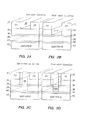
図1a〜dに、ヴィア・ファースト・デュアル・ダマシン構造をエッチングする本発明に基づく方法の概略図を示す。図1aは、酸化シリコンなどの第1の誘電層14、窒化シリコンなどの第1のストップ層16、酸化シリコンなどの第2の誘電層18、窒化シリコンなどの第2のストップ層20およびシリコン・ウェーハなどの基板22の積層の上のフォトレジスト・マスキング層12に、ヴィアに対応する開口10が形成された、エッチング前の状態を示す。図1bは、開口10が誘電層14、18および第1のストップ層16を貫通して第2のストップ層20まで延びた、エッチング後の構造を示す。図1cは、トレンチ24用のマスキング層を再パターニングした後の構造を示す。図1dは、第1の誘電層14が第1のストップ層16までエッチングされたエッチング後の構造を示す。
【0014】
図2a〜dに、トレンチ・ファースト・デュアル・ダマシン構造をエッチングする本発明に基づく方法の概略図を示す。図2aは、酸化シリコンなどの第1の誘電層34、窒化シリコンなどの第1のストップ層36、酸化シリコンなどの第2の誘電層38、窒化シリコンなどの第2のストップ層40およびシリコン・ウェーハなどの基板42の積層の上のフォトレジスト・マスキング層32に、トレンチに対応する開口30が形成された、エッチング前の状態を示す。図2bは、開口30が誘電層34を貫通して第1のストップ層36まで延びた、エッチング後の構造を示す。図2cは、ヴィア44用のマスキング層を再パターニングした後の構造を示す。図2dは、第2の誘電層38が第2のストップ層40までエッチングされたエッチング後の構造を示す。
【0015】
図3a〜bに、単一の段階でデュアル・ダマシン構造をエッチングする本発明に基づく方法の概略図を示す。図3aは、酸化シリコンなどの第1の誘電層54、窒化シリコンなどの第1のストップ層56、酸化シリコンなどの第2の誘電層58、窒化シリコンなどの第2のストップ層60およびシリコン・ウェーハなどの基板62の積層の上のフォトレジスト・マスキング層52に、トレンチに対応する開口50が形成された、エッチング前の状態を示す。単一のエッチング段階で第1のストップ層56を貫通するヴィアをエッチングするため、第1のストップ層56は開口64を含む。図2bは、開口50が誘電層54を貫通して第1のストップ層56まで延び、開口64が第2の誘電体58を貫通して第2のストップ層60まで延びた、エッチング後の構造を示す。このようなアレンジメントを、「自己整合デュアル・ダマシン」構造と呼ぶことができる。
【0016】
本発明のプロセスは、フッ素化酸化シリコン(FSG)などのドープ酸化シリコン、二酸化シリコンなどの無ドープ酸化シリコン、スピン・オン・ガラス(SOG)、リン酸ケイ酸ホウ素ガラス(BPSG)、リン酸ケイ酸塩ガラス(PSG)などのケイ酸塩ガラス、熱成長させたドープまたは無ドープ酸化シリコン、ドープまたは無ドープのTEOSが堆積された酸化シリコンなど、様々な誘電層のエッチングに適用可能である。誘電体ドーパントは、ホウ素、リンおよび/またはヒ素を含む。誘電体は、多結晶シリコン、アルミニウム、銅、チタン、タングステン、モリブデンなどの金属、これらの合金、窒化チタンなどの窒化物、ケイ化チタン、ケイ化コバルト、ケイ化タングステン、ケイ化モリブデンなどの金属ケイ化物などの導電層または半導電層の上に置くことができる。
【0017】
高密度プラズマは、様々なタイプのプラズマ・リアクタで作り出すことができる。このようなプラズマ・リアクタは、一般に、RFエネルギー、マイクロ波エネルギー、磁場などを使用して高密度プラズマを作り出す高エネルギー源を有する。例えば、高密度プラズマは、誘導結合プラズマ・リアクタとも呼ばれるトランスフォーマ・カップルド・プラズマ(TCPTM)、電子サイクロトロン共鳴(ECR)プラズマ・リアクタ、ヘリコン・プラズマ・リアクタなどで発生させることができる。高密度プラズマを作り出すことができる高フロー・プラズマ・リアクタの一例が、本出願と同一人が所有する米国特許出願第08/658261号に開示されている。その開示は、参照によって本明細書に組み込まれる。
【0018】
本発明のプロセスは、図4に示すリアクタ100などの誘導結合プラズマ・リアクタ中で実施することができる。リアクタ100は、リアクタの下壁の出口104に接続された真空ポンプによって所望の真空圧力に維持された内部102を含む。エッチング・ガスは、ガス供給源106から誘電体窓110の下面の周囲に延びるプレナム108にガスを供給するシャワーヘッド・アレンジメントに供給することができる。リアクタの上の誘電体窓110の外側の1回または数回のターンを有する平面らせんコイルなどの外部RFアンテナ114に、RF源112からRFエネルギーを供給することによって、リアクタ内に高密度プラズマを発生させることができる。このプラズマ発生源を、リアクタの上端に真空気密式かつ取外し可能に取り付けられたモジュール式取付けアレンジメントの一部とすることができる。
【0019】
リアクタ内部の基板支持体118の上、例えばリアクタの側壁からモジュール式取付けアレンジメントによって取外し可能に支持された片持ばりチャック・アレンジメントなどの上に、ウェーハなどの半導体基板116が支持される。基板支持体118は、片持ばり式に取り付けられた支持アームの一端にあり、リアクタの側壁の開口を通すことによって、基板支持体/支持アーム・アセンブリ全体をリアクタから取り外すことができる。基板支持体118は、静電チャック120などのチャッキング器具を含むことができ、基板の周囲を、誘電体フォーカス・リング122で取り囲むことができる。チャックは、エッチング・プロセス中に基板にRFバイアスを印加するためのRFバイアシング電極を含むことができる。ガス供給源106によって供給されたエッチング・ガスは、窓110とその下のガス分配プレート124との間のチャネルを流れ、プレート124のガス吐出口を通って内部102に入ることができる。リアクタはさらに、プレート124から円錐形に延びる被加熱ライナ126を含むことができる。
【0020】
一実施形態では、本発明が、自己整合コンタクト(SAC)を含むコンタクト、導線、ヴィアなどの0.3μm以下の高アスペクト比フィーチャを半導体基板の誘電層中にプラズマ・エッチングするプロセスを提供する。このプロセスでは、高密度プラズマ・リアクタ内で、フルオロカーボン、一酸化炭素および任意選択のガス、例えばキャリヤ・ガス(例えばアルゴン)を含むガス混合物にエネルギーを与えて、フルオロカーボンが遊離Fと遊離Cに瞬間的に解離するようなプラズマ状態とする。このエッチング・プロセス中に、一酸化炭素は、高密度プラズマによって遊離Cと遊離酸素とに瞬間的に解離し、この遊離Cが遊離Fの一部と反応して、マスキング層および/またはエッチング・ストップ層のエッチング速度を低下させる。結果的に、COは、エッチング中の誘電材料のエッチング速度と窒化シリコンなどの下層および/またはフォトレジストなどの上層のエッチング速度との間の選択性を所望のレベルにし、同時に、ポリマーのビルドアップの釣り合いをとって、エッチングされたフィーチャの側壁を保護し、一方で過度のポリマー・ビルドアップによるピンチオフおよびエッチ・ストップの問題を回避する効果を有する。エッチ・ストップは特に、大量のポリマーを形成するガス・ケミストリを使用して酸化シリコンなどの誘電材料中に深く幅の狭い開口をプラズマ・エッチングする際に問題となる。すなわち、開口内でのポリマー・ビルドアップが、酸化シリコンのさらなるエッチングを妨げる。本発明のプロセスでは、エッチング・ガス混合物中の一酸化炭素でポリマーを分解する相乗効果によって、ポリマー・ビルドアップを低減させることができる。さらに、エッチングされたフィーチャの微小寸法(CD)を維持するため、COは、エッチングされた開口の側壁から十分な量のポリマー・ビルドアップを除去して、エッチングされた開口の「ピンチオフ」の原因となり、開口を所望の深さまで完全にエッチングするのを妨げる、側壁の過度のポリマー・ビルドアップを回避する。
【0021】
本発明によれば、エッチング・ガス・ケミストリのエッチング速度選択比を制御するのに有効な量の一酸化炭素が加えられる。すなわち、COおよび1種または数種のフルオロカーボン・ガスを含むエッチング・ガスを使用するときには、COが、フルオロカーボンから解離した高密度プラズマ中の遊離Fを捕捉する効果を有する。このような遊離Fは、マスキング層、エッチング・ストップ層などの層を攻撃し、その結果、エッチング速度選択性が低下する。しかし、適当なレベルのCOを供給することによって、選択比を増大させるのに十分な量の遊離Fを捕捉することが可能である。プラズマ・エッチング・リアクタに供給するCOの量は、遊離Fを捕捉し、エッチングされた開口の底のポリマーと反応することによってエッチ・ストップを防ぐのに有効な量とすることが好ましい。平面コイル・アンテナを使用してRFエネルギーをリアクタに誘導結合する高密度プラズマ・リアクタでは、流量50から250sccmのCOをリアクタに供給することによって、本発明の有利な効果が達成される。
【0022】
エッチング・ガス混合物は任意選択で、窒素および/または不活性キャリヤ・ガスなどのその他のガスを含むことができる。アルゴンは、フッ素が酸化シリコンなどの誘電材料を攻撃するのを助ける特に有用な不活性キャリヤ・ガスである。しかし、He、Ne、Krおよび/またはXeなどのその他の不活性ガスを不活性キャリヤ・ガスとして使用することもできる。プラズマ・エッチング・リアクタの圧力を低く維持するため、リアクタに導入するキャリヤ・ガスの流量を小さくすることができる。例えば、高密度プラズマ・リアクタでは、リアクタに供給するアルゴンの量を25から300sccmとすることができる。このキャリヤ・ガスは、誘電体のエッチング速度、例えば酸化物のエッチング速度の増大を、酸化物をスパッタリングすることによって助ける。
【0023】
フルオロカーボンが、xが少なくとも1、yが少なくとも1、zが0かまたは0よりも大きいCxFyHz、例えば、CF4、C3F6、C3F8、C5F8、C4F8、C2F6、CH2F5、C2HF5、CH3F、CH2F2を含むことが好ましい。水素を含むフルオロカーボンはかなり重合性であるが、エッチ・ストップ現象を回避するため、無水素フルオロカーボン・ガスを、相乗効果的なCO追加と組み合わせて使用して、深く幅の狭い開口が達成されるよう重合度を制御することができる。プラズマ・リアクタに供給するフルオロカーボン・ガスの量は、所望の重合度を十分に達成するものでなければならない。一例として、リアクタにRFエネルギーを誘導結合する高密度プラズマ・リアクタでは、流量50から250sccmのCOを供給することができ、総量25から150sccm、好ましくは40から100sccm、より好ましくは60から70sccmのフルオロカーボン・ガスを供給することができる。一例として、直径0.25μmのコンタクト開口に対しては、40〜70sccmのCxFyHzZを供給するときにCO流量を50から200sccmとすることができ、アルゴンを供給する場合には、これを50から150sccmとすることができる。当業者には明白なことだが、これらの各種ガスの流量は、プラズマ・リアクタのタイプ、電力設定、リアクタ中の真空圧力、プラズマ源の解離速度などの因子によって決まる。
【0024】
本発明のプロセスは、少なくとも5:1という極めて高いアスペクト比を得る目的に有用であり、特に、0.3μm未満、好ましくは0.18μm以下の開口について最大10:1のアスペクト比を達成するのに有用である。例えば、2.1μmを超える深さの直径0.25μmの開口に対して、実質的にまっすぐな壁を得ることができる。異方性エッチングを提供するため、基板支持体によって半導体基板にRFバイアスを供給すると有利である。例えば、6、8または12インチ・ウェーハを十分にRFバイアスするためには、基板支持体中のRFバイアシング電極に500から3000ワット程度の電力を供給すればよい。
【0025】
リアクタの圧力は可能な限り低く維持することが好ましい。一般に、リアクタの圧力が低すぎるとプラズマの消滅につながり、リアクタの圧力が高すぎるとエッチ・ストップの問題が生じる可能性がある。高密度プラズマ・リアクタでは、リアクタの圧力が30mTorr未満であることが好ましく、10mTorr未満であるとさらに好ましい。エッチングを受けている半導体基板のところにプラズマが閉じ込められるため、基板表面の真空圧力がリアクタの真空圧力設定よりも高くなる可能性がある。
【0026】
エッチングを受けている半導体基板を支持している基板支持体が、基板上のフォトレジストの焼損を防ぐ(例えば、基板を140℃未満に維持する)ために基板を十分に冷却することが好ましい。高密度プラズマ・リアクタでは、基板支持体を20から40℃に冷却すれば十分である。基板支持体は、ESCなどの下部電極を含むことができ、その上に、シリコン・ウェーハなどの基板を静電的にクランプし、ウェーハとESCの上面との間に所望の圧力のヘリウムを供給することによって基板を冷却する。ウェーハを所望の温度、例えば0から100℃に維持するためには、ウェーハとチャックの間の空間のHeの圧力を10から30Torrに維持すればよい。
【0027】
図4に示したような誘導結合プラズマ・リアクタを用いて本発明を実施するときには、平面コイル・アンテナに、周波数13.46MHz、電力レベル1000から4000ワットのRFエネルギーを供給することができる。この電力は、フルオロカーボンを遊離Fおよび遊離Cに瞬間的に解離させるのに十分なものでなければならない。以前に説明したとおり、このような強いプラズマは、ドープまたは無ドープ酸化シリコン、例えば、無ドープ・ケイ酸塩ガラス(USG)、ケイ酸ホウ素リン・ガラス(BPSG)、ケイ酸リン・ガラス(PSG)、スピン・オン・ガラス(SOG)、ドープまたは無ドープTEOS、フッ素化酸化シリコン(SiOF)、熱酸化物などの誘電材料のエッチング中に選択性の問題を引き起こす。
【0028】
本発明のプロセスは、酸化シリコンを貫通してその下の導電層または半導電層に達する深く幅の狭い開口をエッチングするのに特によく適している。この層は、Al、Ti、Cu、Moなどの金属、これらの合金、窒化チタンなどの金属窒化物、ドープまたは無ドープ多結晶または単結晶シリコン、ケイ化チタン、ケイ化タングステン、ケイ化コバルト、ケイ化モリブデンなどの金属ケイ化物などである。エッチング・ガス混合物に酸素を追加する場合には、この下層導電材料が、酸素によって攻撃される窒化シリコンなどの材料を含まないことが好ましい。
【0029】
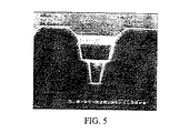
本発明に基づく高密度エッチング・プロセスの一例を以下に示す。LAM Research Corporationから販売されている9100PTXTMなどの誘導結合高密度プラズマ・エッチング・リアクタを使用するときには、真空圧力を5mTorr、リアクタの外側の平面コイル・アンテナへの電力を1300ワット、静電チャック中のRFバイアシング電極への電力を1700ワット、ウェーハとチャックの間に供給するヘリウムを20Torrにそれぞれ設定することができる。図5は、エッチング・ガス混合物:CO 200sccm、CH2F2 35sccm、C4F8 25sccmを用いてエッチングした構造のSEM顕微鏡写真である。
【0030】
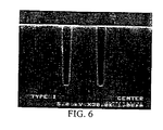
図6〜9は、エッチングしたコンタクトのSEM顕微鏡写真である。フォトレジスト層は取り除かれている。図6および7はそれぞれ、Siストップ層の上のTEOS誘電層中の約50%オーバーエッチングされた直径0.25μm、深さ1.8μmのコンタクト開口の中央および縁部における断面を示す。図8および9はそれぞれ、Si3N4ストップ層の上のPSG誘電層中の約50%オーバーエッチングされた直径0.25μm、深さ1.8μmのコンタクト開口の中央および縁部における断面を示す。
【0031】
下の表1に、さまざまなリアクタ圧力およびCH2F2、C4F8、COガス流量を使用した、デュアル・ダマシン構造のエッチング結果を示す。
【0032】
【表1】

下の表2に、さまざまなサイズの開口についてのエッチング速度およびフォトレジスト・マスキング層のエッチング速度を含む、上の表1のラン番号1〜10に対する試験結果を示す。
【0034】
【表2】
上記試験を実施した結果によれば、本発明のプロセスに基づく誘電体エッチングの最適レジメは次のとおりである。高CO流量でのエッチ・ストップを防ぐためには、チャンバの圧力を10mTorr以下に設定すると有利である。下層の高いエッチング速度選択性を得るためにも、チャンバの圧力を10mTorr以下に維持することが望ましい。しかし、フォトレジスト選択性は、これよりも高いチャンバ圧力設定で高くなるように見える。最適CO流量は、50から200sccmであるようだ。CO流量が250sccm以上のときには、チャンバの圧力設定に関係なくエッチ・ストップが起こる。断面および選択性の目的から最適なエッチング・ガス混合物は、比1:1から1.5:1のCH2F2/C4F8である。さらに、RIEラグの逆転は、低い圧力設定の方が起こりそうである。
【0036】
本発明に基づくプロセスは、以下の構造を有するウェーハに対して実施した以下の測定の結果として開発されたものである。上から順に11600A Iライン・フォトレジスト、20000A TEOS、Si基板を有するウェーハに対するTEOSエッチング速度およびRIEラグの測定、上から順に10000A Iライン・フォトレジスト、3000A Si3N4、1000A熱酸化物、Si基板を有するウェーハに対するSi3N4エッチング速度および選択性の測定、上から順に8250A DUVレジスト、17000A PSG、1000A Si3N4、シリコン基板を有するウェーハに対する0.25μmおよび0.35μmPSGエッチング速度および選択性の測定、上から順に10000A DUVレジスト、18000A TEOS、シリコン基板を有するウェーハ、および6000A DUVレジスト、7000A TEOSトレンチ(CD0.3μmから1.0μm)、1500A Si3N4、10000A TEOSバイア(CD0.35μmから0.60μm)、1500A Si3N4、シリコン基板を有する酸化物デュアル・ダマシン構造ウェーハに対する0.25μmおよび0.35μmTEOSエッチング速度および選択性の測定。深さ1.2μmの0.4μmコンタクトのRIEラグをSEM顕微鏡写真から次式を使用して計算した:RIEラグ=100×(オープン領域のエッチング速度−0.4μmコンタクトのエッチング速度)/オープン領域のエッチング速度。酸化物エッチング速度の均一性の値をSEMから次式を使用して決定した:均一性(%)=(中央フィーチャ・サイズ−縁部フィーチャ・サイズ)×100/(中央フィーチャ・サイズ+縁部フィーチャ・サイズ)。
【0037】
実施した実験の結果、LAM9100PTXTMリアクタを使用した好ましい中央点誘電体エッチング・プロセスは次のとおりである。チャンバ圧力10mTorr、上部電極(TCPコイル)電力1300ワット、下部電極(ESC)電力1500ワット、CH2F2 35sccm、C4F8 25sccm、CO 200sccm。一般に、チャンバ圧力は5から15mTorr、下部電極温度は約+20℃、ウェーハとESCの間に供給するヘリウムは約20Torr、CH2F2流量は30から40sccm、C4F8流量は20から30sccm、CO流量は150から250sccmとすることができる。以上のリアクタ設定によって、高密度プラズマ・リアクタ内でのダマシン構造のエッチングでこれまで得られなかったエッチング速度選択性が達成されたが、最適なリアクタ設定が、リアクタおよびガス・ケミストリの選択によって変化することは当業者には明白であろう。
【0038】
比較実験として、下表3に示すエッチング・ガス・ケミストリを評価した。
【0039】
【表3】
さまざまなパラメータに対する異なるCO流量の影響を下表4に示す。リアクタは、圧力4mTorr、上部電極電力1300ワット、下部電極電力1600ワット、CH2F2 36sccm、C4F8 24sccm、Ar 100sccm、ウェーハ裏面冷却用He 20Torrで動作させた。
【0041】
【表4】
本発明に基づくプロセスによって達成された追加の結果を図10〜13に示す。図10は、CO流量に対するTEOSエッチング速度のグラフである。◆はオープン領域のエッチング速度を指示し、■は0.4μm開口のエッチング速度を指示する。このグラフに示すとおり、開口のエッチング速度は意外にも、50sccmまではCO流量の増大とともに急速に増大し、CO流量50〜200sccmではまずまず一定である。一方、オープン領域のエッチング速度はCOを追加しないときに最大であり、CO流量が200sccmまで増大するにつれ0近くまで低下する。
【0043】
図11は、CO流量に対するTEOSエッチング深度のグラフである。◆は0.4μm開口のエッチング深度を指示する。このグラフに示すとおり、開口のエッチング深度は、CO流量200sccmまで徐々に増大する。
【0044】
図12は、CO流量に対する選択性のグラフである。◆はTEOS:Si3N4選択性を指示し、■はTEOS:フォトレジスト(PR)選択性を指示する。このグラフに示すとおり、エッチング・ガスがCOを含まないときのTEOS:PR選択性は3未満であり、CO流量が50sccmまで増大するにつれ5に近づく。一方、TEOS:Si3N4選択性は、COを追加しないと10未満であり、CO流量が200sccmまで増大すると15に増大する。
【0045】
図13は、CO流量に対するRIEラグのグラフである。◆は、COを0から200sccmまで増大させたときのオープン領域と比較した0.4μm開口のエッチング速度比を指示する。このグラフに示すとおり、50sccm以上のCOではRIEラグが負となり、オープン領域がコンタクト開口よりもゆっくりとエッチングされることを指示している。
【0046】
本発明の原理、好ましい実施形態および動作モードを以上に説明した。しかし、本発明を、以上に論じた特定の実施形態に限定されると解釈してはならない。以上に記載した実施形態は例示的なものと考えるべきであって、限定的なものと考えるべきではなく、請求項によって定義される本発明の範囲から逸脱することなく、これらの実施形態に当業者が変更を加えることができることを理解されたい。
【図面の簡単な説明】
【図1a〜d】 本発明のプロセスに基づいてエッチングすることができるバイア・ファースト・デュアル・ダマシン構造の概略図である。図1aはエッチング前の状態、図1bは、バイアが既にエッチングされたエッチング後の状態、図1cは、トレンチ・エッチング用に再パターニングされた構造、図1dは、トレンチが既にエッチングされたエッチング後の状態をそれぞれ示す。
【図2a〜d】 本発明のプロセスに基づいてエッチングすることができるトレンチ・ファースト・デュアル・ダマシン構造の概略図である。図2aはエッチング前の状態、図2bは、トレンチが既にエッチングされたエッチング後の状態、図2cは、バイア・エッチング用に再パターニングされた構造、図2dは、バイアが既にエッチングされたエッチング後の状態をそれぞれ示す。
【図3a〜b】 本発明のプロセスに基づいてエッチングすることができる自己整合デュアル・ダマシン構造の概略図である。図3aはエッチング前の状態、図3bは、トレンチおよびバイアが既にエッチングされたエッチング後の状態をそれぞれ示す。
【図4】 本発明のプロセスを実施する目的に使用することができる誘導結合高密度プラズマ・リアクタの概略図である。
【図5】 本発明に基づいてエッチングされたデュアル・ダマシン構造のSEM顕微鏡写真である。
【図6】 本発明に基づいてエッチングされたウェーハの中央のTEOS/Si構造のSEM顕微鏡写真である。
【図7】 本発明に基づいてエッチングされたウェーハの縁部のTEOS/Si構造のSEM顕微鏡写真である。
【図8】 本発明に基づいてエッチングされたウェーハの中央のPSG/Si3N4構造のSEM顕微鏡写真である。
【図9】 本発明に基づいてエッチングされたウェーハの縁部のPSG/Si3N4構造のSEM顕微鏡写真である。
【図10】 TEOSのエッチング速度に対するCO流量の影響を示すグラフである。エッチング速度は50sccmCOまで着実に増大した。
【図11】 TEOSのエッチング深度に対するCO流量の影響を示すグラフである。エッチング速度は200sccmCOまで着実に増大した。
【図12】 CO流量に対する選択性のグラフである。
【図13】 CO流量に対するRIEラグのグラフである。50sccmを超えるCO流量に対してはRIEラグが負数となった。[0001]
(Field of Invention)
The present invention relates to an improved method for plasma etching dielectric materials such as silicon oxide in the manufacture of integrated circuits.
[0002]
(Background of the Invention)
A common requirement in integrated circuit manufacturing is the etching of contacts, vias, etc. openings in the dielectric material. Dielectric materials include doped silicon oxide such as fluorinated silicon oxide (FSG) (doped silicon oxide), undoped silicon oxide such as silicon dioxide (undoped silicon oxide), and boron phosphate silicate glass (BPSG). Silicate glasses such as phosphate silicate glass (PSG), thermally grown doped or undoped silicon oxide, silicon oxide with doped or undoped TEOS deposited, and the like. The dielectric dopant includes boron, phosphorus and / or arsenic. Dielectrics include metals such as polycrystalline silicon, aluminum, copper, titanium, tungsten, molybdenum, alloys thereof, nitrides such as titanium nitride, metals such as titanium silicide, cobalt silicide, tungsten silicide, molybdenum silicide, etc. It may be placed on a conductive or semiconductive layer such as a silicide.
[0003]
Various plasma etching techniques for etching openings in silicon oxide are described in U.S. Pat. Nos. 5,013,398, 5,031,400, 5,021,211, 5,022,958, 5,269,879, 5,529,657, 5,595,627, 5,611,888, And in US Pat. No. 5,780,338. Plasma etching may be performed using a parallel plate type plasma reactor chamber described in the above-mentioned 5013398 patent, a medium density reactor such as the triode type reactor described in the above-mentioned 5013400 patent, or an inductively coupled reactor described in the above-mentioned patent 5529657. It can be carried out in a high density reactor. The etching gas chemistry includes oxygen-free Ar / CHF described in the above-mentioned 5021121 and 5022958 patents. 3 / CF 4 (Optional) Gas mixture, oxygen-free fluorine-containing nitrogen gas mixture described in the above-mentioned 5269879 patent, C described in the above-mentioned 5595627 patent 4 F 8 / CO gas mixture, oxygen / CF as described in the aforementioned 5013400 patent 4 Gas mixture, oxygen / CF as described in the aforementioned 5529657 patent 4 / CH 4 Gas mixtures, and the Freon / neon gas mixtures described in the aforementioned US Pat. No. 5,611,888.
[0004]
US Pat. No. 5,736,457 describes single and dual “damascene” metallization processes. In the “single damascene” method, vias and conductors are formed in separate stages. At each of these stages, the metallization pattern for the conductor or via is etched into the dielectric layer, the trench or via hole in the etched dielectric layer is filled with a metal layer, and excess metal is chemically Remove by mechanical planarization (CMP) or etch back process. In the “dual damascene” method, via and conductor metallization patterns are etched into the dielectric layer, and the etched trenches and via openings are filled with a single metal fill / excess metal removal process.
[0005]
The medium density plasma reactor operates at a higher chamber pressure than the high density plasma reactor, and the degree of dissociation of the etching gas chemistry is lower than that of the high density plasma reactor. For example, in a medium density plasma reactor, C 4 F 8 Etching gas such as C 4 F 8 → C 2 F 8 → CF 2 → Dissociate stepwise as CF + F. Such stepwise dissociation can increase the etch rate of the dielectric layer and decrease the etch rate of the layer above it, such as a photoresist, or the layer below it, such as an etch stop layer. Such a ratio of etch rates is referred to as an “etch selectivity” and the high selectivity obtained in a medium density plasma reactor facilitates complete etching of contacts, vias and conductor patterns. In contrast, in a high-density reactor, the etch gas instantaneously dissociates, resulting in higher etch rates for the masking layer and the etch stop layer, resulting in a lower selectivity. For example, in a high density plasma reactor, C 4 F 8 Directly dissociates into free F, and this high free F content leads to rapid etching of the masking layer and / or the etch stop layer, which results in an unacceptably low etch selectivity.
[0006]
As device geometries get smaller and smaller, the need for high etch selectivity to plasma etch deep and narrow openings in dielectric layers such as silicon oxide is growing. Therefore, there is a need in the art for high density plasma etching techniques that provide high etch selectivity and / or achieve deep and narrow apertures. Furthermore, it would be highly desirable if such an aperture geometry could be achieved without causing bowing of the aperture sidewalls.
[0007]
(Summary of Invention)
The present invention provides a method for plasma etching a dielectric layer. The method includes introducing a semiconductor substrate including a conductive or semiconductive layer under a masking layer and a dielectric layer into a high density plasma etch reactor. The dielectric layer can be etched in a single step to expose the conductive layer or semiconductive layer and form an opening extending through the dielectric layer to the conductive layer or semiconductive layer. Etching is performed in a high density plasma etch reactor by exposing the dielectric layer to an ionized etch gas comprising a fluorocarbon reactant, carbon monoxide, and an optional inert carrier gas. In this method, the fluorocarbon is instantaneously dissociated into free F and free C by the high-density plasma, and carbon monoxide has an effect of increasing the selectivity of the etching rate of the dielectric layer with respect to the etching rate of the masking layer. Only exist.
[0008]
According to one aspect of the invention, the dielectric layer comprises silicon oxide such as doped or undoped silicon dioxide, BPSG, PSG, TEOS, thermally oxidized silicon, and the openings correspond to conductor patterns, via openings or contact openings. Including grooves. According to another aspect of the invention, the openings can be etched so that the aspect ratio is at least 3: 1. Etching gas is C x F y H z The hydrogen-containing and / or hydrogen-free fluorocarbon reactant represented by can be included. Where x is at least 1, y is at least 1, and z is 0 or greater than 0. For example, the fluorocarbon reactant is CF 4 , C 4 F 8 , C 2 F 6 , C 3 F 6 , C 3 F 8 , C 5 F 8 , CH 3 F, C 2 HF 5 And / or CH 2 F 2 Can be selected from the group consisting of The conductive layer or semiconductive layer may be Al, Al alloy, Cu, Cu alloy, Ti, Ti alloy, doped or undoped polycrystalline or single crystal silicon, TiN, TiW, and / or Ti, W, Co, Mo A metal-containing layer selected from the group consisting of compounds and the like can be included.
[0009]
The process of the present invention provides an aperture of 0.30 μm in depth with a depth of at least 1.8 μm, in particular 0.25 μm or less, with a C of 1 to 5, y of 1 to 8, and z of 0 to 3. x F y H z Etching can be performed using a fluorocarbon reactant containing. As an example, the fluorocarbon reactant is C 2 HF 5 , CH 2 F 2 , C 2 F 6 , C 3 F 6 , C 4 F 8 And one or several gases selected from these and mixtures thereof. The optional carrier gas can be selected from the group consisting of Ar, He, Ne, Kr, Xe and mixtures thereof. CO can be supplied to the plasma reactor at a flow rate of 25 to 250 sccm, fluorocarbon can be supplied to the plasma reactor at a flow rate of 5 to 100 sccm, and the optional carrier gas can be 10 to 300 sccm. The plasma reactor can be supplied at a flow rate. As an example, CO, fluorocarbon, and Ar can be supplied to the plasma reactor at flow rates of 50 to 200 sccm, 40 to 70 sccm, and 50 to 150 sccm, respectively. During the etching phase, the high density plasma reactor is preferably maintained at a vacuum pressure of less than 10 mTorr. After the etching step, the opening can be filled with metal. The method of the present invention can further include the steps of forming a photoresist layer on the dielectric layer and patterning the photoresist layer to form a plurality of openings, wherein the etching step comprises conducting wires, via openings or contacts. An opening metallization pattern is formed in the dielectric layer. Using this method, an opening having an aspect ratio of at least 5: 1 can be formed. In this method, free F liberated by the dissociation of the fluorocarbon reacts with carbon monoxide, and the effect of free F attacking the masking layer is reduced.
[0010]
Thus, the method of the present invention provides a semiconductor manufacturing process that can plasma etch deep, narrow, sub-¼ micron openings in dielectric materials such as doped and undoped silicon oxide. The plasma gas chemistry includes fluorocarbons and CO that cooperate to etch the dielectric material while providing the desired selectivity with respect to the masking and stop layers.
[0011]
(Detailed description of the invention)
The present invention provides a process for high density plasma etching of features such as contacts, vias, conductors, etc. in dielectric materials such as oxide layers in integrated circuit manufacturing. The present invention overcomes the problems of conventional etching techniques where the selectivity between the dielectric etch rate and the masking layer and stop layer etch rates is too low for commercial application. In the present invention, such selectivity problems are solved by utilizing an etching gas chemistry that reduces the etching rate of the masking layer and / or the stop layer.
[0012]
According to one aspect of the present invention, the oxide: photoresist etch selectivity greater than 5: 1 and the doped and undoped oxide films (BPSG, PSG, TEOS) at least 1. A single or dual damascene etch process is provided that can be etched to an etch depth of 8 μm. This process reduces or reverses the RIE lag, thereby enabling multi-level dielectric etch applications and dual damascene device fabrication.
[0013]
1a-d show a schematic diagram of a method according to the invention for etching via first dual damascene structures. FIG. 1a shows a
[0014]
2a-d show a schematic diagram of a method according to the invention for etching a trench first dual damascene structure. FIG. 2a shows a
[0015]
Figures 3a-b show a schematic diagram of a method according to the invention for etching a dual damascene structure in a single stage. FIG. 3a shows a
[0016]
The process of the present invention includes doped silicon oxide such as fluorinated silicon oxide (FSG), undoped silicon oxide such as silicon dioxide, spin-on-glass (SOG), boron silicate glass (BPSG), and silicon phosphate. It is applicable to the etching of various dielectric layers such as silicate glass such as silicate glass (PSG), thermally grown doped or undoped silicon oxide, silicon oxide deposited with doped or undoped TEOS. The dielectric dopant includes boron, phosphorus and / or arsenic. Dielectrics include metals such as polycrystalline silicon, aluminum, copper, titanium, tungsten, molybdenum, alloys thereof, nitrides such as titanium nitride, metals such as titanium silicide, cobalt silicide, tungsten silicide, molybdenum silicide, etc. It can be placed on a conductive or semiconductive layer such as a silicide.
[0017]
High density plasmas can be produced in various types of plasma reactors. Such plasma reactors typically have a high energy source that uses RF energy, microwave energy, magnetic fields, etc. to create a high density plasma. For example, high-density plasma is known as transformer coupled plasma (TCP), also called inductively coupled plasma reactor. TM ), Electron cyclotron resonance (ECR) plasma reactor, helicon plasma reactor, and the like. An example of a high flow plasma reactor capable of producing a high density plasma is disclosed in US patent application Ser. No. 08 / 658,261, owned by the same applicant as the present application. The disclosure of which is incorporated herein by reference.
[0018]
The process of the present invention can be performed in an inductively coupled plasma reactor, such as
[0019]
A
[0020]
In one embodiment, the present invention provides a process for plasma etching a high aspect ratio feature of 0.3 μm or less, such as contacts, conductors, vias, including self-aligned contacts (SAC), into a dielectric layer of a semiconductor substrate. This process energizes a gas mixture containing fluorocarbon, carbon monoxide and an optional gas, such as a carrier gas (eg, argon), in a high-density plasma reactor so that the fluorocarbon instantaneously becomes free F and free C. In a plasma state that dissociates automatically. During this etching process, the carbon monoxide is instantaneously dissociated into free C and free oxygen by the high density plasma, and this free C reacts with a part of the free F to form the masking layer and / or the etching layer. Reduce the etch rate of the stop layer. As a result, CO provides the desired level of selectivity between the etch rate of the dielectric material being etched and the etch rate of the lower layer such as silicon nitride and / or the upper layer such as photoresist, while at the same time building up the polymer This has the effect of protecting the etched feature sidewalls while avoiding pinch-off and etch stop problems due to excessive polymer build-up. Etch stops are particularly problematic when plasma etching deep and narrow openings in dielectric materials such as silicon oxide using gas chemistry that forms large amounts of polymer. That is, polymer buildup within the opening prevents further etching of the silicon oxide. The process of the present invention can reduce polymer build-up due to the synergistic effect of decomposing the polymer with carbon monoxide in the etching gas mixture. In addition, to maintain the minute dimension (CD) of the etched features, the CO removes a sufficient amount of polymer buildup from the etched opening sidewalls to cause "pinch-off" of the etched opening. And avoiding excessive polymer build-up of the sidewalls that prevent the opening from being completely etched to the desired depth.
[0021]
In accordance with the present invention, an amount of carbon monoxide is added that is effective to control the etch rate selectivity of the etching gas chemistry. That is, when using an etching gas containing CO and one or several fluorocarbon gases, CO has the effect of capturing free F in the high-density plasma dissociated from the fluorocarbon. Such free F attacks layers such as the masking layer and the etching stop layer, and as a result, the etching rate selectivity decreases. However, by supplying the appropriate level of CO, it is possible to capture a sufficient amount of free F to increase the selectivity. The amount of CO supplied to the plasma etch reactor is preferably an amount effective to trap free F and react with the polymer at the bottom of the etched opening to prevent etch stop. In a high density plasma reactor that inductively couples RF energy to the reactor using a planar coil antenna, the advantageous effects of the present invention are achieved by supplying the reactor with a flow rate of 50 to 250 sccm of CO.
[0022]
The etching gas mixture can optionally include other gases such as nitrogen and / or inert carrier gas. Argon is a particularly useful inert carrier gas that helps fluorine attack dielectric materials such as silicon oxide. However, other inert gases such as He, Ne, Kr and / or Xe can also be used as the inert carrier gas. In order to keep the pressure of the plasma etching reactor low, the flow rate of the carrier gas introduced into the reactor can be reduced. For example, in a high density plasma reactor, the amount of argon supplied to the reactor can be between 25 and 300 sccm. This carrier gas helps to increase the dielectric etch rate, such as the oxide etch rate, by sputtering the oxide.
[0023]
A fluorocarbon in which x is at least 1, y is at least 1 and z is 0 or greater than C x F y H z For example, CF 4 , C 3 F 6 , C 3 F 8 , C 5 F 8 , C 4 F 8 , C 2 F 6 , CH 2 F 5 , C 2 HF 5 , CH 3 F, CH 2 F 2 It is preferable to contain. Fluorocarbons containing hydrogen are quite polymerizable, but to avoid the etch stop phenomenon, a hydrogenless fluorocarbon gas is used in combination with synergistic CO addition to achieve deep and narrow openings. The degree of polymerization can be controlled. The amount of fluorocarbon gas supplied to the plasma reactor must be sufficient to achieve the desired degree of polymerization. As an example, in a high density plasma reactor that inductively couples RF energy to the reactor, a flow rate of 50 to 250 sccm of CO can be supplied, for a total amount of 25 to 150 sccm, preferably 40 to 100 sccm, more preferably 60 to 70 sccm. -Gas can be supplied. As an example, for a contact opening with a diameter of 0.25 μm, a C of 40-70 sccm x F y H z When supplying Z, the CO flow rate can be 50 to 200 sccm, and when supplying argon, this can be 50 to 150 sccm. As will be apparent to those skilled in the art, the flow rates of these various gases depend on factors such as the type of plasma reactor, power settings, vacuum pressure in the reactor, and dissociation rate of the plasma source.
[0024]
The process of the present invention is useful for the purpose of obtaining very high aspect ratios of at least 5: 1, in particular to achieve an aspect ratio of up to 10: 1 for apertures of less than 0.3 μm, preferably 0.18 μm or less. Useful for. For example, a substantially straight wall can be obtained for an opening with a diameter of 0.25 μm that is deeper than 2.1 μm. In order to provide anisotropic etching, it is advantageous to provide an RF bias to the semiconductor substrate by the substrate support. For example, in order to sufficiently RF bias a 6, 8 or 12 inch wafer, power of about 500 to 3000 watts may be supplied to the RF biasing electrode in the substrate support.
[0025]
The reactor pressure is preferably kept as low as possible. In general, reactor pressures that are too low can lead to plasma extinction, while reactors that are too high can cause etch stop problems. In a high density plasma reactor, the reactor pressure is preferably less than 30 mTorr, and more preferably less than 10 mTorr. Since the plasma is confined to the semiconductor substrate being etched, the vacuum pressure on the substrate surface can be higher than the vacuum pressure setting of the reactor.
[0026]
It is preferred that the substrate support that supports the semiconductor substrate undergoing etching sufficiently cool the substrate to prevent photoresist burnout on the substrate (eg, maintain the substrate below 140 ° C.). In a high density plasma reactor, it is sufficient to cool the substrate support to 20 to 40 ° C. The substrate support can include a bottom electrode, such as an ESC, on which a substrate, such as a silicon wafer, is electrostatically clamped to provide the desired pressure of helium between the wafer and the top surface of the ESC. To cool the substrate. In order to maintain the wafer at a desired temperature, for example, 0 to 100 ° C., the He pressure in the space between the wafer and the chuck may be maintained at 10 to 30 Torr.
[0027]
When implementing the present invention using an inductively coupled plasma reactor as shown in FIG. 4, a planar coil antenna can be supplied with RF energy at a frequency of 13.46 MHz and a power level of 1000 to 4000 watts. This power must be sufficient to instantaneously dissociate the fluorocarbon into free F and free C. As previously described, such intense plasmas can be doped or undoped silicon oxide such as undoped silicate glass (USG), boron silicate phosphorous glass (BPSG), phosphorous silicate glass (PSG). ), Causing selectivity problems during etching of dielectric materials such as spin-on-glass (SOG), doped or undoped TEOS, fluorinated silicon oxide (SiOF), thermal oxide.
[0028]
The process of the present invention is particularly well suited for etching deep, narrow openings that penetrate silicon oxide and reach the underlying conductive or semiconductive layer. This layer is made of metals such as Al, Ti, Cu, Mo, alloys thereof, metal nitrides such as titanium nitride, doped or undoped polycrystalline or single crystal silicon, titanium silicide, tungsten silicide, cobalt silicide, Metal silicides such as molybdenum silicide. When oxygen is added to the etching gas mixture, it is preferred that the underlying conductive material does not include materials such as silicon nitride that are attacked by oxygen.
[0029]
An example of a high density etching process according to the present invention is shown below. 9100PTX sold by LAM Research Corporation TM When using an inductively coupled high density plasma etch reactor, such as 5 mTorr vacuum pressure, 1300 watts to the planar coil antenna outside the reactor, 1700 watts to the RF biasing electrode in the electrostatic chuck The helium supplied between the wafer and the chuck can be set to 20 Torr. FIG. 5 shows an etching gas mixture:
[0030]
6-9 are SEM micrographs of the etched contacts. The photoresist layer has been removed. FIGS. 6 and 7 show cross sections at the center and edge of a contact opening of about 0.25 μm diameter and 1.8 μm depth, respectively, about 50% over-etched in the TEOS dielectric layer above the Si stop layer. 8 and 9 are respectively Si 3 N 4 FIG. 6 shows a cross-section at the center and edge of a contact opening with a diameter of 0.25 μm and a depth of 1.8 μm, approximately 50% over-etched in the PSG dielectric layer above the stop layer.
[0031]
Table 1 below shows the various reactor pressures and CH 2 F 2 , C 4 F 8 , Shows the etching results of a dual damascene structure using a CO gas flow rate.
[0032]
[Table 1]
Table 2 below shows the test results for run numbers 1-10 in Table 1 above, including etch rates for various sized openings and photoresist mask layer etch rates.
[0034]
[Table 2]
According to the results of the above tests, the optimum regime for dielectric etching based on the process of the present invention is as follows. In order to prevent etch stop at high CO flow rates, it is advantageous to set the chamber pressure to 10 mTorr or less. In order to obtain a high etching rate selectivity of the lower layer, it is desirable to maintain the chamber pressure at 10 mTorr or lower. However, the photoresist selectivity appears to be higher at higher chamber pressure settings. The optimal CO flow rate appears to be 50 to 200 sccm. When the CO flow rate is 250 sccm or more, an etch stop occurs regardless of the chamber pressure setting. An optimum etch gas mixture for cross-section and selectivity purposes is a CH ratio of 1: 1 to 1.5: 1. 2 F 2 / C 4 F 8 It is. Furthermore, RIE lag inversion is more likely to occur at lower pressure settings.
[0036]
The process according to the present invention was developed as a result of the following measurements performed on a wafer having the following structure. 11600A I line photoresist, 20,000A TEOS, TEOS etch rate and RIE lag measurements on wafer with Si substrate, 10000A I line photoresist, 3000A Si from top to bottom 3 N 4 Si for wafers with 1000A thermal oxide, Si substrate 3 N 4 Measurement of etching rate and selectivity, 8250A DUV resist, 17000A PSG, 1000A Si in order from the top 3 N 4 , 0.25 μm and 0.35 μm PSG etch rate and selectivity measurements for wafers with silicon substrate, 10000A DUV resist, 18000A TEOS, wafer with silicon substrate, and 6000A DUV resist, 7000A TEOS trench (CD 0.3 μm from top to bottom) To 1.0 μm), 1500 A Si 3 N 4 10,000 A TEOS via (CD 0.35 μm to 0.60 μm), 1500 A Si 3 N 4 , 0.25 μm and 0.35 μm TEOS etch rate and selectivity measurements for oxide dual damascene wafers with silicon substrates. The RIE lag of a 0.4 μm contact with a depth of 1.2 μm was calculated from the SEM micrograph using the following formula: RIE lag = 100 × (open region etch rate−0.4 μm contact etch rate) / open region Etching rate. Oxide etch rate uniformity values were determined from the SEM using the following equation: Uniformity (%) = (center feature size−edge feature size) × 100 / (center feature size + edge) Feature size).
[0037]
As a result of the experiment conducted, LAM9100PTX TM A preferred center point dielectric etch process using a reactor is as follows.
[0038]
As a comparative experiment, etching gas chemistry shown in Table 3 below was evaluated.
[0039]
[Table 3]
The effect of different CO flow rates on various parameters is shown in Table 4 below. The reactor has a pressure of 4 mTorr, an upper electrode power of 1300 watts, a lower electrode power of 1600 watts, CH 2 F 2 36 sccm, C 4 F 8 The operation was performed at 24 sccm,
[0041]
[Table 4]
Additional results achieved by the process according to the present invention are shown in FIGS. FIG. 10 is a graph of TEOS etch rate versus CO flow rate. ◆ indicates the etching rate of the open region, and ■ indicates the etching rate of the 0.4 μm opening. As shown in this graph, the etching rate of the opening is surprisingly increased as the CO flow rate is increased up to 50 sccm, and is constant at a CO flow rate of 50 to 200 sccm. On the other hand, the etching rate in the open region is maximum when no CO is added, and decreases to near zero as the CO flow rate increases to 200 sccm.
[0043]
FIG. 11 is a graph of TEOS etch depth versus CO flow rate. ◆ indicates the etching depth of the 0.4 μm opening. As shown in this graph, the etching depth of the opening gradually increases to a CO flow rate of 200 sccm.
[0044]
FIG. 12 is a graph of selectivity versus CO flow rate. ◆ TEOS: Si 3 N 4 Selectivity is indicated, and ▪ indicates TEOS: photoresist (PR) selectivity. As shown in this graph, the TEOS: PR selectivity is less than 3 when the etching gas does not contain CO and approaches 5 as the CO flow rate increases to 50 sccm. On the other hand, TEOS: Si 3 N 4 Selectivity is less than 10 without adding CO and increases to 15 when the CO flow rate is increased to 200 sccm.
[0045]
FIG. 13 is a graph of RIE lag versus CO flow rate. The ♦ indicates the etching rate ratio of the 0.4 μm opening compared to the open region when CO is increased from 0 to 200 sccm. As shown in this graph, the RIE lag is negative for CO of 50 sccm or more, indicating that the open region is etched more slowly than the contact opening.
[0046]
The principles, preferred embodiments and modes of operation of the present invention have been described above. However, this invention should not be construed as limited to the particular embodiments discussed above. The embodiments described above are to be regarded as illustrative and not restrictive, and are intended to cover these embodiments without departing from the scope of the invention as defined by the claims. It should be understood that the merchant can make changes.
[Brief description of the drawings]
1a-d are schematic views of via-first dual damascene structures that can be etched according to the process of the present invention. FIG. 1a is the state before etching, FIG. 1b is the state after etching with the via already etched, FIG. 1c is the re-patterned structure for trench etching, and FIG. 1d is after the etching with the trench already etched. Each state is shown.
Figures 2a-d are schematic illustrations of a trench first dual damascene structure that can be etched according to the process of the present invention. 2a is the state before etching, FIG. 2b is the state after etching with the trench already etched, FIG. 2c is the re-patterned structure for via etching, and FIG. 2d is after the etching with the via already etched. Each state is shown.
Figures 3a-b are schematics of a self-aligned dual damascene structure that can be etched according to the process of the present invention. FIG. 3a shows the state before etching, and FIG. 3b shows the state after etching in which the trenches and vias have already been etched.
FIG. 4 is a schematic diagram of an inductively coupled high density plasma reactor that can be used to implement the process of the present invention.
FIG. 5 is a SEM micrograph of a dual damascene structure etched according to the present invention.
FIG. 6 is a SEM micrograph of the TEOS / Si structure in the center of a wafer etched according to the present invention.
FIG. 7 is a SEM micrograph of a TEOS / Si structure at the edge of a wafer etched in accordance with the present invention.
FIG. 8: PSG / Si in the center of a wafer etched according to the present invention 3 N 4 It is a SEM micrograph of a structure.
FIG. 9 shows PSG / Si at the edge of a wafer etched according to the invention. 3 N 4 It is a SEM micrograph of a structure.
FIG. 10 is a graph showing the effect of CO flow rate on the etching rate of TEOS. The etching rate steadily increased to 50 sccm CO.
FIG. 11 is a graph showing the effect of CO flow rate on the etching depth of TEOS. The etching rate steadily increased to 200 sccmCO.
FIG. 12 is a graph of selectivity versus CO flow rate.
FIG. 13 is a graph of RIE lag versus CO flow rate. The RIE lag was negative for CO flow rates over 50 sccm.
Claims (22)
誘電層の上にマスキング層を有し、前記誘電層の下に導電層または半導電層を有する半導体基板を、高密度プラズマ・エッチング・リアクタの中に導入する段階と、
フルオロカーボン反応物C4F8およびCH2F2ならびに一酸化炭素から成るエッチング・ガスを前記プラズマ・エッチング・リアクタに供給し、前記エッチング・ガスにエネルギーを与えて高密度プラズマ状態にする段階と、
前記マスキング層および前記誘電層の露出部分を前記高密度プラズマに暴露して、前記高密度プラズマで前記誘電層中に開口がエッチングされるようにする段階と、
を含み、
前記マスキング層のエッチング速度に対する前記誘電層のエッチング速度の比が少なくとも5であり、
前記プラズマ・エッチング・リアクタに供給されるフルオロカーボン反応物に対する一酸化炭素の体積流量比は2.15:1から5:1の範囲であり、
前記フルオロカーボン反応物および一酸化炭素の流量は、それぞれ25から150sccmおよび50から250sccmであり、
前記誘電層は、ドープまたは無ドープ酸化シリコン膜を含み、
前記高密度プラズマは、RFエネルギーを前記プラズマ・エッチング・リアクタに誘導結合することによって形成される、
方法。A method of etching a dielectric layer comprising:
Introducing a semiconductor substrate having a masking layer over a dielectric layer and having a conductive layer or semiconductive layer under the dielectric layer into a high density plasma etch reactor;
The fluorocarbon reactant C 4 F 8 and CH 2 F 2 and formed Ru etchant gas from the carbon monoxide fed to the plasma etching reactor, phase and that high density plasma state by applying energy to the etching gas ,
Exposing exposed portions of the masking layer and the dielectric layer to the high density plasma such that openings are etched in the dielectric layer with the high density plasma;
Including
The ratio of the etching rate of the dielectric layer to the etching rate of the masking layer is at least 5 ;
The volume flow ratio of carbon monoxide to fluorocarbon reactant fed to the plasma etch reactor ranges from 2.15: 1 to 5: 1 ;
The flow rates of the fluorocarbon reactant and carbon monoxide are 25 to 150 sccm and 50 to 250 sccm, respectively.
The dielectric layer includes a doped or undoped silicon oxide film,
The high-density plasma, Ru is formed by inductively coupling RF energy to the plasma etching reactor,
Method.
Applications Claiming Priority (3)
| Application Number | Priority Date | Filing Date | Title |
|---|---|---|---|
| US09/163,301 | 1998-09-30 | ||
| US09/163,301 US6297163B1 (en) | 1998-09-30 | 1998-09-30 | Method of plasma etching dielectric materials |
| PCT/US1999/020888 WO2000019506A1 (en) | 1998-09-30 | 1999-09-24 | Method of plasma etching dielectric materials |
Publications (3)
| Publication Number | Publication Date |
|---|---|
| JP2002526919A JP2002526919A (en) | 2002-08-20 |
| JP2002526919A5 JP2002526919A5 (en) | 2006-11-09 |
| JP4499289B2 true JP4499289B2 (en) | 2010-07-07 |
Family
ID=22589392
Family Applications (1)
| Application Number | Title | Priority Date | Filing Date |
|---|---|---|---|
| JP2000572915A Expired - Fee Related JP4499289B2 (en) | 1998-09-30 | 1999-09-24 | Method for plasma etching a dielectric material |
Country Status (7)
| Country | Link |
|---|---|
| US (1) | US6297163B1 (en) |
| EP (1) | EP1121714A1 (en) |
| JP (1) | JP4499289B2 (en) |
| KR (1) | KR20010082216A (en) |
| AU (1) | AU6246399A (en) |
| TW (1) | TW584672B (en) |
| WO (1) | WO2000019506A1 (en) |
Families Citing this family (26)
| Publication number | Priority date | Publication date | Assignee | Title |
|---|---|---|---|---|
| US6518591B1 (en) * | 1998-12-02 | 2003-02-11 | Cypress Semiconductor Corporation | Contact monitor, method of forming same and method of analizing contact-, via- and/or trench-forming processes in an integrated circuit |
| TW434816B (en) * | 1998-12-28 | 2001-05-16 | Asahi Chemical Micro Syst | Method for forming contact hole |
| US6797189B2 (en) | 1999-03-25 | 2004-09-28 | Hoiman (Raymond) Hung | Enhancement of silicon oxide etch rate and nitride selectivity using hexafluorobutadiene or other heavy perfluorocarbon |
| US6251770B1 (en) * | 1999-06-30 | 2001-06-26 | Lam Research Corp. | Dual-damascene dielectric structures and methods for making the same |
| US6749763B1 (en) * | 1999-08-02 | 2004-06-15 | Matsushita Electric Industrial Co., Ltd. | Plasma processing method |
| US20050158666A1 (en) * | 1999-10-15 | 2005-07-21 | Taiwan Semiconductor Manufacturing Company, Ltd. | Lateral etch inhibited multiple etch method for etching material etchable with oxygen containing plasma |
| JP3586605B2 (en) * | 1999-12-21 | 2004-11-10 | Necエレクトロニクス株式会社 | Method for etching silicon nitride film and method for manufacturing semiconductor device |
| US6432318B1 (en) * | 2000-02-17 | 2002-08-13 | Applied Materials, Inc. | Dielectric etch process reducing striations and maintaining critical dimensions |
| KR100727834B1 (en) * | 2000-09-07 | 2007-06-14 | 다이킨 고교 가부시키가이샤 | Dry etching gas and method for dry etching |
| KR100379976B1 (en) * | 2000-11-27 | 2003-04-16 | 삼성전자주식회사 | Etching gas composition of silicone oxides and method of etching silicone oxides using the same |
| KR100782632B1 (en) * | 2000-12-21 | 2007-12-06 | 동경 엘렉트론 주식회사 | Etching method for insulating film |
| KR100434312B1 (en) * | 2000-12-21 | 2004-06-05 | 주식회사 하이닉스반도체 | Method for making contact hole in semiconductor device |
| US6740593B2 (en) * | 2002-01-25 | 2004-05-25 | Micron Technology, Inc. | Semiconductor processing methods utilizing low concentrations of reactive etching components |
| US6593232B1 (en) | 2002-07-05 | 2003-07-15 | Taiwan Semiconductor Manufacturing Co., Ltd | Plasma etch method with enhanced endpoint detection |
| US6838012B2 (en) | 2002-10-31 | 2005-01-04 | Lam Research Corporation | Methods for etching dielectric materials |
| US7083903B2 (en) * | 2003-06-17 | 2006-08-01 | Lam Research Corporation | Methods of etching photoresist on substrates |
| US6949469B1 (en) | 2003-12-16 | 2005-09-27 | Lam Research Corporation | Methods and apparatus for the optimization of photo resist etching in a plasma processing system |
| US7504340B1 (en) * | 2004-06-14 | 2009-03-17 | National Semiconductor Corporation | System and method for providing contact etch selectivity using RIE lag dependence on contact aspect ratio |
| US20070287301A1 (en) | 2006-03-31 | 2007-12-13 | Huiwen Xu | Method to minimize wet etch undercuts and provide pore sealing of extreme low k (k<2.5) dielectrics |
| TW201415551A (en) * | 2006-03-31 | 2014-04-16 | Applied Materials Inc | Method to improve the step coverage and pattern loading for dielectric films |
| JP5382937B2 (en) * | 2007-01-05 | 2014-01-08 | エプコス アクチエンゲゼルシャフト | Etching method with improved control of feature critical dimension at the bottom of thick film |
| US7985681B2 (en) * | 2007-06-22 | 2011-07-26 | Micron Technology, Inc. | Method for selectively forming symmetrical or asymmetrical features using a symmetrical photomask during fabrication of a semiconductor device and electronic systems including the semiconductor device |
| US8603363B1 (en) * | 2012-06-20 | 2013-12-10 | Praxair Technology, Inc. | Compositions for extending ion source life and improving ion source performance during carbon implantation |
| JP2014007270A (en) * | 2012-06-25 | 2014-01-16 | Tokyo Electron Ltd | Etching method and etching apparatus |
| CN103824767B (en) * | 2012-11-16 | 2017-05-17 | 中微半导体设备(上海)有限公司 | Method for etching deep through-silicon-via |
| JP6557642B2 (en) * | 2016-09-05 | 2019-08-07 | 株式会社日立ハイテクノロジーズ | Plasma processing apparatus and plasma processing method |
Family Cites Families (26)
| Publication number | Priority date | Publication date | Assignee | Title |
|---|---|---|---|---|
| US5013400A (en) | 1990-01-30 | 1991-05-07 | General Signal Corporation | Dry etch process for forming champagne profiles, and dry etch apparatus |
| US5021121A (en) | 1990-02-16 | 1991-06-04 | Applied Materials, Inc. | Process for RIE etching silicon dioxide |
| US5013398A (en) | 1990-05-29 | 1991-05-07 | Micron Technology, Inc. | Anisotropic etch method for a sandwich structure |
| US5022958A (en) | 1990-06-27 | 1991-06-11 | At&T Bell Laboratories | Method of etching for integrated circuits with planarized dielectric |
| US6238588B1 (en) * | 1991-06-27 | 2001-05-29 | Applied Materials, Inc. | High pressure high non-reactive diluent gas content high plasma ion density plasma oxide etch process |
| US6171974B1 (en) * | 1991-06-27 | 2001-01-09 | Applied Materials, Inc. | High selectivity oxide etch process for integrated circuit structures |
| US5269879A (en) | 1991-10-16 | 1993-12-14 | Lam Research Corporation | Method of etching vias without sputtering of underlying electrically conductive layer |
| JPH06188229A (en) * | 1992-12-16 | 1994-07-08 | Tokyo Electron Yamanashi Kk | Posttreatment of etching |
| JP3271359B2 (en) * | 1993-02-25 | 2002-04-02 | ソニー株式会社 | Dry etching method |
| JP3252518B2 (en) * | 1993-03-19 | 2002-02-04 | ソニー株式会社 | Dry etching method |
| US5770098A (en) | 1993-03-19 | 1998-06-23 | Tokyo Electron Kabushiki Kaisha | Etching process |
| KR100264445B1 (en) | 1993-10-04 | 2000-11-01 | 히가시 데쓰로 | Plasma treatment equipment |
| JPH07161702A (en) | 1993-10-29 | 1995-06-23 | Applied Materials Inc | Plasma etching of oxide |
| US5736457A (en) | 1994-12-09 | 1998-04-07 | Sematech | Method of making a damascene metallization |
| JP3778299B2 (en) | 1995-02-07 | 2006-05-24 | 東京エレクトロン株式会社 | Plasma etching method |
| US5626716A (en) | 1995-09-29 | 1997-05-06 | Lam Research Corporation | Plasma etching of semiconductors |
| US5843847A (en) * | 1996-04-29 | 1998-12-01 | Applied Materials, Inc. | Method for etching dielectric layers with high selectivity and low microloading |
| JP3319285B2 (en) * | 1996-06-05 | 2002-08-26 | 株式会社日立製作所 | Plasma processing apparatus and plasma processing method |
| JP3862035B2 (en) * | 1996-07-17 | 2006-12-27 | ソニー株式会社 | Semiconductor device and manufacturing method thereof |
| JP3997494B2 (en) * | 1996-09-17 | 2007-10-24 | ソニー株式会社 | Semiconductor device |
| DE69733962T2 (en) * | 1996-10-11 | 2006-05-24 | Tokyo Electron Ltd. | PLASMA-etching method |
| JP3713869B2 (en) * | 1997-02-17 | 2005-11-09 | ソニー株式会社 | Manufacturing method of semiconductor device |
| US5972235A (en) * | 1997-02-28 | 1999-10-26 | Candescent Technologies Corporation | Plasma etching using polycarbonate mask and low pressure-high density plasma |
| US5780338A (en) | 1997-04-11 | 1998-07-14 | Vanguard International Semiconductor Corporation | Method for manufacturing crown-shaped capacitors for dynamic random access memory integrated circuits |
| GB9712019D0 (en) * | 1997-06-09 | 1997-08-06 | Northern Telecom Ltd | Eye measurement of optical sampling |
| US6051504A (en) | 1997-08-15 | 2000-04-18 | International Business Machines Corporation | Anisotropic and selective nitride etch process for high aspect ratio features in high density plasma |
-
1998
- 1998-09-30 US US09/163,301 patent/US6297163B1/en not_active Expired - Lifetime
-
1999
- 1999-09-24 WO PCT/US1999/020888 patent/WO2000019506A1/en not_active Application Discontinuation
- 1999-09-24 KR KR1020017004035A patent/KR20010082216A/en active Application Filing
- 1999-09-24 JP JP2000572915A patent/JP4499289B2/en not_active Expired - Fee Related
- 1999-09-24 AU AU62463/99A patent/AU6246399A/en not_active Abandoned
- 1999-09-24 EP EP99949628A patent/EP1121714A1/en not_active Withdrawn
-
2000
- 2000-01-13 TW TW088116761A patent/TW584672B/en not_active IP Right Cessation
Also Published As
| Publication number | Publication date |
|---|---|
| EP1121714A1 (en) | 2001-08-08 |
| WO2000019506A9 (en) | 2000-08-31 |
| KR20010082216A (en) | 2001-08-29 |
| WO2000019506A1 (en) | 2000-04-06 |
| AU6246399A (en) | 2000-04-17 |
| TW584672B (en) | 2004-04-21 |
| US6297163B1 (en) | 2001-10-02 |
| JP2002526919A (en) | 2002-08-20 |
Similar Documents
| Publication | Publication Date | Title |
|---|---|---|
| JP4499289B2 (en) | Method for plasma etching a dielectric material | |
| US6617257B2 (en) | Method of plasma etching organic antireflective coating | |
| US6670278B2 (en) | Method of plasma etching of silicon carbide | |
| US6962879B2 (en) | Method of plasma etching silicon nitride | |
| WO2002080230A2 (en) | Method of plasma etching low-k organosilicate materials | |
| US6630407B2 (en) | Plasma etching of organic antireflective coating | |
| KR100628932B1 (en) | Method for etching silicon dioxide using fluorocarbon gas chemistry | |
| US7547635B2 (en) | Process for etching dielectric films with improved resist and/or etch profile characteristics | |
| US7166535B2 (en) | Plasma etching of silicon carbide | |
| US6746961B2 (en) | Plasma etching of dielectric layer with etch profile control | |
| US20020142610A1 (en) | Plasma etching of dielectric layer with selectivity to stop layer | |
| JP2002525840A (en) | In situ integrated oxide etching process especially useful for copper dual damascene | |
| US6136722A (en) | Plasma etching method for forming hole in masked silicon dioxide | |
| EP1147549A1 (en) | Method of etching silicon dioxide using hydrogen-containing additive gases in fluorocarbon gas chemistry | |
| US6969685B1 (en) | Etching a dielectric layer in an integrated circuit structure having a metal hard mask layer | |
| US5908320A (en) | High selectivity BPSG:TiSi2 contact etch process | |
| KR20070020325A (en) | Method of plasma etching dielectric materials | |
| JP2003163205A (en) | Oxidation film etching method |
Legal Events
| Date | Code | Title | Description |
|---|---|---|---|
| A521 | Request for written amendment filed |
Free format text: JAPANESE INTERMEDIATE CODE: A523 Effective date: 20060920 |
|
| A621 | Written request for application examination |
Free format text: JAPANESE INTERMEDIATE CODE: A621 Effective date: 20060920 |
|
| A977 | Report on retrieval |
Free format text: JAPANESE INTERMEDIATE CODE: A971007 Effective date: 20090907 |
|
| A131 | Notification of reasons for refusal |
Free format text: JAPANESE INTERMEDIATE CODE: A131 Effective date: 20090911 |
|
| A521 | Request for written amendment filed |
Free format text: JAPANESE INTERMEDIATE CODE: A523 Effective date: 20091106 |
|
| A131 | Notification of reasons for refusal |
Free format text: JAPANESE INTERMEDIATE CODE: A131 Effective date: 20091207 |
|
| A521 | Request for written amendment filed |
Free format text: JAPANESE INTERMEDIATE CODE: A523 Effective date: 20100226 |
|
| TRDD | Decision of grant or rejection written | ||
| A01 | Written decision to grant a patent or to grant a registration (utility model) |
Free format text: JAPANESE INTERMEDIATE CODE: A01 Effective date: 20100326 |
|
| A01 | Written decision to grant a patent or to grant a registration (utility model) |
Free format text: JAPANESE INTERMEDIATE CODE: A01 |
|
| A61 | First payment of annual fees (during grant procedure) |
Free format text: JAPANESE INTERMEDIATE CODE: A61 Effective date: 20100415 |
|
| FPAY | Renewal fee payment (event date is renewal date of database) |
Free format text: PAYMENT UNTIL: 20130423 Year of fee payment: 3 |
|
| R150 | Certificate of patent or registration of utility model |
Free format text: JAPANESE INTERMEDIATE CODE: R150 |
|
| LAPS | Cancellation because of no payment of annual fees |