JP4498528B2 - Thermo-optic effect type optical deflection element and thermo-optic effect type optical deflection element module using the same - Google Patents
Thermo-optic effect type optical deflection element and thermo-optic effect type optical deflection element module using the same Download PDFInfo
- Publication number
- JP4498528B2 JP4498528B2 JP2000092354A JP2000092354A JP4498528B2 JP 4498528 B2 JP4498528 B2 JP 4498528B2 JP 2000092354 A JP2000092354 A JP 2000092354A JP 2000092354 A JP2000092354 A JP 2000092354A JP 4498528 B2 JP4498528 B2 JP 4498528B2
- Authority
- JP
- Japan
- Prior art keywords
- waveguide layer
- thermo
- effect type
- optic effect
- type optical
- Prior art date
- Legal status (The legal status is an assumption and is not a legal conclusion. Google has not performed a legal analysis and makes no representation as to the accuracy of the status listed.)
- Expired - Fee Related
Links
Images


Landscapes
- Optical Modulation, Optical Deflection, Nonlinear Optics, Optical Demodulation, Optical Logic Elements (AREA)
Description
【0001】
【発明の属する技術分野】
本発明は熱光学効果型光偏光素子に関し、特に最大偏向角が大きいものである。
【0002】
【従来の技術】
従来の光偏向素子としては、半導体の導波路に回折格子が形成されてなり、電圧印加による量子閉じ込めシュタルク効果(QCSE)を利用したものがある。
図14は従来の光偏向素子の一例を示したもので、素子の光軸に平行な断面および光軸に垂直な断面の双方を示した図である。この図に示す光偏向素子1は、n−InP基板2の上にn−InPバッファ層3、井戸層とバリア層が交互に積層された多重量子井戸(Multi Quantum Well)層4が順次積層され、その上に導波路層5がストライプ状に形成され、フォトリソグラフィー・エッチング技術により導波路層5の上に回折格子6が形成されたものである。そして、導波路層5の上にはp−InPクラッド層7が形成されるとともに、その側方にはポリイミド層8が形成されている。また、この積層構造の下面には下部電極層9が、光の入射面と反対側の端面に近い側の上面には上部電極層10が形成されている。また、これらの電極層9、10は、例えばCrとAuとの積層構造などからなる金属膜で構成されている。なお、寸法の一例としては、素子1の光軸方向の長さが3〜4mm程度、上部電極層9の一辺が100μm程度である。
【0003】
このような構成の光偏向素子1に光S0を入射すると、回折格子6の作用によりブラッグの式に従う回折角をもって光は上方に回折するが、この際、上部、下部電極層9、10間に電圧(逆バイアス)を印加すると、量子閉じ込めシュタルク効果により電圧の大きさに見合う量だけ導波路層5の屈折率が変化するため、屈折率変化に伴って光S1が回折する角度が変化する。したがって、電圧の大きさを調節することにより、回折光S1を所望の角度(偏向角)だけ偏向させて、導波路層5の光信号の進行方向側(プラス側)に傾いた回折光S2あるいはその反対側(マイナス側)に傾いた回折光S3を得ることができる。
なお、偏向していない回折光S1の位置を中心として導波路層5の進行方向側(S3側)と反対方向側(S2側)とに偏向させることができる角度の合計(Ψ)を最大偏向角いう。また、単に偏向角という場合は回折光S1 の位置をゼロとし、導波路層5の光信号の進行方向側に偏向したときの角度をプラス、反対側に偏向したときの角度をマイナスで表したものとする。
この回折光の偏向機能を利用することによって、光コンピュータにおける光スイッチングや並列光情報伝送システムなどの光インターコネクションに、この光偏向素子1を送信側素子として適用することができる。
【0004】
【発明が解決しようとする課題】
しかしながら、量子閉じ込めシュタルク効果による屈折率変化は光の吸収量の増大を伴う。すなわち、導波路層5における屈折率変化を大きくすると信号光の損失が大きくなるため、実用上、屈折率変化量は約0.3%程度が限界であり、最大偏向角は10度程度が限界であった。
本発明は前記事情に鑑みてなされたもので、最大偏向角を大きくすることができる光偏向素子を提供することを課題とする。
【0005】
【課題を解決するための手段】
前記課題を解決するため、本発明の熱光学効果型光偏向素子は、回折格子が形成されたプラスチック製の導波路層と、この導波路層の外周に形成され、かつこの導波路層よりも低屈折率のプラスチック製のクラッド層を備え、前記導波路層の一端から入射された光を回折格子の作用により回折光として導波路層の上方の外部空間に出射する光偏向素子であって、前記導波路層の回折格子は、導波路層の上部に周期的な鋸歯状の凹凸を形成して構成され、前記クラッド層のうち、導波路層の上側に位置して回折光が通過する部分が外方に向けて凸状となっており、前記導波路層から出射される回折光の光路を避ける位置にヒータが配置されており、このヒータによって、前記導波路層の温度を変化させて回折光の偏向角を変化させるようにしたことを特徴とする。
また、この熱光学効果型光偏向素子を筐体に収めて光学効果型光偏向素子モジュールを構成することができる。
【0006】
【発明の実施の形態】
図1は本発明の熱光学効果型光偏向素子の一例を示したもので、素子の光軸に平行な断面および光軸に垂直な断面の双方を示した図である。この熱光学効果型光偏向素子21は、長方形板状の基板22の上にクラッド層23が形成され、その内部に断面略正方形の柱状の導波路層24が形成されている。導波路層24は光を導波するため前記クラッド層23よりも高屈折率である。なお、導波路層24の上面には回折格子24aが形成されており、クラッド層23の上面には導波路層24をはさんでヒータ25、26が対称に設けられている。ヒータ25は、導波路層24の長さ方向に平行な直線状のヒータ部25aと、その両端部に設けられた外部電極を装着するための電極パット部25b、25bとから構成されている。ヒータ26も同様に直線状の26aとその両端部の電極パット部26b、26bとから構成されている。
【0007】
基板22としては表面を酸化処理したシリコン基板などが用いられる。
導波路層24は、熱光学効果が大きいたため、プラスチックから形成され、例えばシリコーン樹脂、フッ化ポリイミド樹脂などのポリイミド系樹脂、フッ化メタクリレートなどのメタクリル系樹脂などが用いられるが、ポリイミド系樹脂が好ましい。クラッド層23は好ましくは導波路層24の材料として例示したものと同様のプラスチックなどから形成される。
具体的なクラッド層23および導波路層24の材料としては、特開平9−21920号公報に開示されている、複屈折の大きさが同程度の2種類のポリイミドの共重合体などを用いることができる。この2種類のポリイミドの例としては、例えば2,2−ビス(3,4−ジカルボキシフェニル)ヘキサフルオロプロパン二無水物(6FDB)と2,2’−ビス(トリフルオロメチル)−4,4’−ジアミノビフェニル(TFDB)から合成されるポリイミド(6FDA/TFDB)と、6FDAと4,4’−オキシジアニリン(4,4’−ODA)から合成されるポリイミド(6FDA/4,4’−ODA)などを挙げることができる。そして、これらのポリイミドの共重合比を変更することによって、導波路層24とクラッド層23との屈折率差を変化させることができる。
ヒータ25、26は金属製の薄膜からなり、特に限定するものではないが、例えば金(Au)、チタン(Ti)、白金(Pt)、クロム(Cr)、ニクロム(NiCr合金)、タングステン(W)などが用いられる。
【0008】
この熱光学効果型光偏向素子21は、例えば以下のようにして製造することができる。
基板22の上に、スピンコート法などにより、導波路層24の下のクラッド層23の厚さに相当する下部クラッド層を形成し、その上面全体に導波路層24の厚さに相当する導波路形成層を形成する。そして、この導波路形成層を導波路層24のパターンに沿ってイオンエッチング法などによって加工して導波路層24を形成するとともに、導波路層24の周囲に下部クラッド層を露出させる。そして、さらにスピンコート法などにより、これら下部クラッド層と導波路層24の上に上部クラッド層を形成し、下部クラッド層と上部クラッド層とが一体化したクラッド層23を完成させる。
ついで、このクラッド層23上に、蒸着法などによって上述のヒータ25、26の材料として例示した金属などからなる導電体薄膜を形成し、この導電体薄膜を加工してパターンを形成し、ヒータ25、26を完成させる。この加工方法としては、フォトリソグラフィーなどを適用することができる。
【0009】
このような構成の熱光学効果型光偏向素子に、図2に示したように光S0を入射すると、回折格子24aの作用によりブラッグの式に従う回折角をもって光は上方に回折する。
この際、図3に示したようにヒータ25、26を作動させると導波路層24の温度が変化し、熱光学効果によって導波路層24の屈折率が変化する。そして、この屈折率変化に伴って光S1が偏向する。したがって、ヒータ25、26によって導波路層24の温度を調節することにより、回折光S1を偏向させて、素子のクラッド層23の上面から所定の角度で偏向した回折光S2またはS3を外部空間に出射することができる。
熱光学効果型光偏向素子において、偏向角θは以下の式で表される。
【0010】
【数1】

【0011】
寸法の一例としては、熱光学効果型光偏向素子21の厚さが約1mm、導波路層24の長さ方向に平行な長さが20mm、これに直交する幅方向の長さが5mmであり、基板22の厚さが1mm、クラッド層23の厚さが30μm、回折格子24aの断面寸法が略7μm×7μm、ヒータ25、26のヒータ部25a、26aの長さが16mmである。
なお、回折格子24aの周期Λは、光の波長λ0、導波路層の実効屈折率、所望の最大偏向角などによって適宜選択されるが、例えば700〜1400μmの範囲とされる。
【0012】
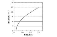
図4は、この寸法例にしたがって回折格子24aの周期Λを1027nmとして製造した熱光学効果型光偏向素子21において、導波路層24の温度と偏向角との関係を示したものであって、波長1.55μmの信号光を入射した状態でヒータ25、26に印加する電圧を変化させることによって偏向角を変化させたときの値である。
なお、この熱光学効果型光偏向素子は、周期Λを調節することにより、137.5℃で偏向角がゼロ(図2におけるS1の位置)になるように設定されており、温度が25〜300℃の範囲で変化する間に、回折光の出射方向(偏向角)はプラス側(図2におけるS3側)、すなわち光信号の進行方向側から、徐々に垂直(0度)になり、さらに反対側のマイナス側(図2におけるS2側)に変化する。その結果、最大偏向角は25度程度となる。
図5は 横軸に示した各最高温度において、最高温度と室温(25℃)との中間の温度のときに1次回折光の偏向角が0度になるように周期Λを設定した熱光学効果型光偏向素子を用意し、各熱光学効果型光偏向素子において、波長1.55μmの光信号を入射した状態で、室温(25℃)から最高温度まで温度を変化させたときの最大偏向角を示したシミュレーション結果である。すなわち、Λは最高温度毎に異なる。最高温度を大きく設定する程、最大偏向角が大きくなることがわかる。
【0013】
図6は本発明の熱光学効果型光偏向素子の他の例を示したもので、図1に示したものと異なるのは、導波路層24の基板22との対向面に回折格子24aが形成され、ヒータ25、26が基板22とクラッド層23との間に設けられている点である。
ヒータ25の両端部の電極パット部25b、25bの上には、それぞれクラッド層23を貫通するスルーホール25c、25cが設けられ、クラッド層23の上面のこれらスルーホール25c、25の周囲には、外部電極を装着する電極パッド部25d、25dが設けられている。電極パッド部25d、25dは電極パット部25b、25bと同様の導電性材料からなり、スルーホール25c、25cの内面にも同様の導電性材料からなる薄膜層が形成されている。その結果、電極パッド部25d、25dに外部電極から電力を印加すると、スルーホール25c、25の内面と電極パット部25bを介してヒータ部25a、25aの温度が上昇し、導波路層24が加熱される。
ヒータ26にも同様にスルーホール26cと、クラッド層23の上面に形成された電極パッド部26dが設けられている。
【0014】
また、図7に示したように導波路層24の直下にひとつのヒータ27を設けた構成とすることもできる。
このヒータ27は、導波路層24の長さ方向に平行な直線状のヒータ部27aと、その両端部に設けられた外部電極を装着するための電極パット部27b、27bを有し、一方の電極パッド27dの上にはクラッド層23の側面と上面に開口するスルーホール27dが設けられ、クラッド層23の上面のスルーホール27dの周囲には、外部電極を装着する電極パッド部27cが設けられている。
他方の電極パット部27bの上には、クラッド層23を貫通するスルーホール27eが設けられ、クラッド層23の上面のスルーホール27eの周囲には、外部電極を装着する電極パッド部27fが設けられている。
本発明においては、導波路層24の温度を変化させることができればヒータの数、位置などは特に限定せず、図6、図7に示した熱光学効果型光偏向素子においても図1に示したものと同様の効果が得られる。
【0015】
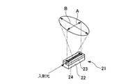
なお、従来の石英系材料からクラッド層23を形成した場合は、図8に示したようにクラッド層23の上面は平坦になる。その結果、図9に示したように、回折光を構成する光の成分のうち、導波路層24と平行な方向の成分Aは広がりにくいが、導波路層24に直交する方向の成分Bは広がりやすく、集光させにくくなる。
一方、本発明の熱光学効果型光偏向素子はクラッド層23がプラスチックからなるため、熱光学効果型光偏向素子の製造工程において、図10に示したようにクラッド層23が硬化する際に導波路層24の上のクラッド層23の上面が収縮し、凸状となる。そしてこの凸状の部分がレンズの役割を果たし、図11に示したように成分Bが広がりにくくなるという利点がある。そのため、回折光を容易に集光させることができる。
【0016】
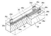
図12は本発明の熱光学効果型光偏向素子を用いた熱光学効果型光偏向素子モジュール31の構成の一例を示したものである。符号33は中空直方体状の筐体であって、この筐体33は本体31と板状の蓋32とからなり、蓋には回折光を取り出す窓32aが設けられている。熱光学効果型光偏向素子21はこの筐体33内に収められ、外部の光ファイバ35がこの熱光学効果型光偏向素子21にコネクタ34を介して接続されている。筐体33は通常アルミニウム、コバール(FeNiCo合金)などから形成したものが用いられる。
本発明の熱光学効果型光偏向素子モジュールの構成は、このように回折光を取り出すことのできる構成を備えた筐体内に熱光学効果型光偏向素子が収められ、かつ熱光学効果型光偏向素子が、この熱光学効果型光偏向素子に光を入射する手段と接続されていればその構成について特に制限はなく、用途に応じて種々の形態を選択することができる。
【0017】
図13はこの熱光学効果型光偏向素子モジュール30を用いた光スイッチングモジュールの構成例を示したもので、板状のベース36の上に熱光学効果型光偏向素子モジュール30が配置されている。光ファイバ35を介して光信号を熱光学効果型光偏向素子モジュール30に入射し、得られた回折光は窓32aからマイクロレンズアレイ37、導波素子38を介して出力ポート39から出射されるようになっている。
【0018】
【発明の効果】
以上説明したように本発明の熱光学効果型光偏向素子は、回折格子が形成されたプラスチック製の導波路層と、この導波路層の外周上に形成され、かつこの導波路層よりも低屈折率のプラスチック製のクラッド層と、該導波路層を加熱するヒータが設けられた熱光学効果型光偏向素子であって、当該ヒータによる前記導波路層の温度を変化させることにより、回折光の偏向角を変化させるものであるため、最大偏向角を従来よりも格段に大きくすることができる。
【図面の簡単な説明】
【図1】 本発明の熱光学効果型光偏向素子の一例を示したもので、素子の光軸に平行な断面および光軸に垂直な断面の双方を示した図である。
【図2】 図1に示した熱光学効果型光偏向素子の回折光の偏向の様子を示した説明図である。
【図3】 図2に示した熱光学効果型光偏向素子のヒータによる導波路層の加熱の様子を示した説明図である。
【図4】 本発明の熱光学効果型光偏向素子の導波路層の温度と偏向角の関係を示したグラフである。
【図5】 本発明の熱光学効果型光偏向素子の導波路層の温度と最大偏向角の関係を示したグラフである。
【図6】 本発明の熱光学効果型光偏向素子の他の例を示したもので、素子の光軸に平行な断面および光軸に垂直な断面の双方を示した図である。
【図7】 本発明の熱光学効果型光偏向素子の他の例を示したもので、素子の光軸に平行な断面および光軸に垂直な断面の双方を示した図である。
【図8】 石英系材料を用いた熱光学効果型光偏向素子の回折光の状態を説明した断面図である。
【図9】 石英系材料を用いた熱光学効果型光偏向素子の回折光の状態を説明した斜視図である。
【図10】 本発明の熱光学効果型光偏向素子の回折光の状態を説明した断面図である。
【図11】 本発明の熱光学効果型光偏向素子の回折光の状態を説明した斜視図である。
【図12】 本発明の熱光学効果型光偏向素子を用いた熱光学効果型光偏向素子モジュールの構成の一例を示した斜視図である。
【図13】 図12に示した熱光学効果型光偏向素子モジュールを用いた光スイッチングモジュールの構成例を示した概略構成図である。
【図14】 従来の光偏向素子の一例を示したもので、素子の光軸に平行な断面および光軸に垂直な断面の双方を示した図である。
【符号の説明】
21…熱光学効果型光偏向素子、23…クラッド層、24…導波路層、
24a…回折格子、25、26…ヒータ、25a、26a…ヒータ部、
30…熱光学効果型光偏向素子モジュール、33…筐体。[0001]
BACKGROUND OF THE INVENTION
The present invention relates to a thermo-optic effect type optical polarizing element, and particularly has a large maximum deflection angle.
[0002]
[Prior art]
As a conventional optical deflecting element, there is an optical deflecting element in which a diffraction grating is formed in a semiconductor waveguide and uses a quantum confined Stark effect (QCSE) by voltage application.
FIG. 14 shows an example of a conventional optical deflection element, and shows both a cross section parallel to the optical axis of the element and a cross section perpendicular to the optical axis. In the optical deflection element 1 shown in this figure, an n-InP buffer layer 3 and a multi quantum well layer 4 in which well layers and barrier layers are alternately stacked are sequentially stacked on an n-InP substrate 2. The
[0003]
When the light S 0 is incident on the optical deflecting element 1 having such a configuration, the light is diffracted upward with a diffraction angle according to the Bragg equation by the action of the diffraction grating 6. When a voltage (reverse bias) is applied to, the refractive index of the
Note that the total angle (Ψ) that can be deflected in the traveling direction side (S 3 side) and the opposite direction side (S 2 side) of the
By utilizing this diffracted light deflection function, the optical deflection element 1 can be applied as a transmission side element to optical interconnections such as optical switching and parallel optical information transmission system in an optical computer.
[0004]
[Problems to be solved by the invention]
However, the refractive index change due to the quantum confined Stark effect is accompanied by an increase in the amount of light absorption. That is, if the refractive index change in the
The present invention has been made in view of the above circumstances, and an object of the present invention is to provide an optical deflection element capable of increasing the maximum deflection angle.
[0005]
[Means for Solving the Problems]
In order to solve the above-described problems, a thermo-optic effect type optical deflection element of the present invention is formed of a plastic waveguide layer on which a diffraction grating is formed, an outer periphery of the waveguide layer, and more than the waveguide layer. A light deflection element comprising a plastic clad layer having a low refractive index, and emitting light incident from one end of the waveguide layer as diffracted light to an external space above the waveguide layer by the action of a diffraction grating, The diffraction grating of the waveguide layer is formed by forming periodic sawtooth irregularities on the upper portion of the waveguide layer, and a portion of the cladding layer that is located above the waveguide layer and through which diffracted light passes Is convex toward the outside, and a heater is disposed at a position that avoids the optical path of the diffracted light emitted from the waveguide layer. The heater changes the temperature of the waveguide layer. It was to change the deflection angle of the diffracted light And wherein the door.
Further, the optical effect type optical deflection element module can be configured by housing the thermo-optical effect type optical deflection element in a casing.
[0006]
DETAILED DESCRIPTION OF THE INVENTION
FIG. 1 shows an example of a thermo-optic effect type optical deflection element of the present invention, and is a diagram showing both a cross section parallel to the optical axis of the element and a cross section perpendicular to the optical axis. In the thermo-optic effect type
[0007]
As the
Since the
As specific materials for the
The
[0008]
The thermo-optic effect type
A lower clad layer corresponding to the thickness of the
Next, a conductor thin film made of the metal exemplified as the material of the above-described
[0009]
When the light S 0 is incident on the thermo-optic effect type optical deflection element having such a configuration as shown in FIG. 2, the light is diffracted upward with a diffraction angle according to the Bragg equation by the action of the
At this time, when the
In the thermo-optic effect type optical deflection element, the deflection angle θ is expressed by the following equation.
[0010]
[Expression 1]
[0011]
As an example of the dimensions, the thickness of the thermo-optic effect type
The period Λ of the
[0012]
FIG. 4 shows the relationship between the temperature of the
This thermo-optic effect type optical deflection element is set so that the deflection angle becomes zero (position of S 1 in FIG. 2) at 137.5 ° C. by adjusting the period Λ, and the temperature is 25. While changing in the range of ˜300 ° C., the diffracted light emission direction (deflection angle) gradually becomes vertical (0 degree) from the plus side (S 3 side in FIG. 2), that is, the optical signal traveling direction side. Further, it changes to the opposite minus side (S 2 side in FIG. 2). As a result, the maximum deflection angle is about 25 degrees.
Fig. 5 shows the thermo-optic effect in which the period Λ is set so that the deflection angle of the first-order diffracted light becomes 0 degrees at the maximum temperature shown on the horizontal axis and at an intermediate temperature between the maximum temperature and room temperature (25 ° C). Maximum deflection angle when the temperature is changed from room temperature (25 ° C.) to the maximum temperature in a state where an optical signal with a wavelength of 1.55 μm is incident on each thermo-optic effect type optical deflection element. It is the simulation result which showed. That is, Λ differs for each maximum temperature. It can be seen that the maximum deflection angle increases as the maximum temperature is set higher.
[0013]
FIG. 6 shows another example of the thermo-optic effect type optical deflecting element of the present invention. The difference from the one shown in FIG. 1 is that a
On the
Similarly, the
[0014]
In addition, as shown in FIG. 7, a configuration in which one
The
A through hole 27e penetrating the
In the present invention, the number and position of the heaters are not particularly limited as long as the temperature of the
[0015]
When the clad
On the other hand, in the thermo-optic effect type optical deflection element of the present invention, since the
[0016]
FIG. 12 shows an example of the configuration of a thermo-optic effect type optical
The configuration of the thermo-optic effect type optical deflection element module of the present invention is such that the thermo-optic effect type optical deflection element is housed in a housing having a configuration capable of taking out diffracted light in this way, and the thermo-optic effect type optical deflection is provided. As long as the element is connected to means for entering light into the thermo-optic effect type optical deflection element, there is no particular limitation on its configuration, and various forms can be selected according to the application.
[0017]
FIG. 13 shows an example of the configuration of an optical switching module using the thermo-optic effect type optical
[0018]
【The invention's effect】
As described above, the thermo-optic effect type optical deflection element of the present invention is formed of a plastic waveguide layer on which a diffraction grating is formed and an outer periphery of the waveguide layer, and is lower than the waveguide layer. A thermo-optic effect type optical deflecting element provided with a plastic clad layer having a refractive index and a heater for heating the waveguide layer, and diffracting light by changing the temperature of the waveguide layer by the heater. Therefore, the maximum deflection angle can be remarkably increased as compared with the prior art.
[Brief description of the drawings]
FIG. 1 shows an example of a thermo-optic effect optical deflection element of the present invention, and is a diagram showing both a cross section parallel to the optical axis of the element and a cross section perpendicular to the optical axis.
FIG. 2 is an explanatory view showing a state of deflection of diffracted light by the thermo-optic effect type optical deflection element shown in FIG. 1;
3 is an explanatory view showing a state of heating a waveguide layer by a heater of the thermo-optic effect type optical deflection element shown in FIG. 2; FIG.
FIG. 4 is a graph showing the relationship between the temperature of the waveguide layer and the deflection angle of the thermo-optic effect type optical deflection element of the present invention.
FIG. 5 is a graph showing the relationship between the temperature of the waveguide layer and the maximum deflection angle of the thermo-optic effect type optical deflection element of the present invention.
FIG. 6 shows another example of the thermo-optic effect type optical deflection element of the present invention, and is a diagram showing both a cross section parallel to the optical axis of the element and a cross section perpendicular to the optical axis.
FIG. 7 shows another example of the thermo-optic effect type optical deflection element of the present invention, and is a diagram showing both a cross section parallel to the optical axis of the element and a cross section perpendicular to the optical axis.
FIG. 8 is a cross-sectional view illustrating a state of diffracted light of a thermo-optic effect type optical deflection element using a quartz-based material.
FIG. 9 is a perspective view illustrating a state of diffracted light of a thermo-optic effect type optical deflection element using a quartz-based material.
FIG. 10 is a cross-sectional view illustrating the state of diffracted light of the thermo-optic effect type optical deflection element of the present invention.
FIG. 11 is a perspective view explaining the state of diffracted light of the thermo-optic effect type optical deflection element of the present invention.
FIG. 12 is a perspective view showing an example of the configuration of a thermo-optic effect type optical deflection element module using the thermo-optic effect type optical deflection element of the present invention.
13 is a schematic configuration diagram showing a configuration example of an optical switching module using the thermo-optic effect type optical deflection element module shown in FIG.
FIG. 14 shows an example of a conventional optical deflection element, and shows both a cross section parallel to the optical axis of the element and a cross section perpendicular to the optical axis.
[Explanation of symbols]
21 ... Thermo-optic effect type optical deflection element, 23 ... Cladding layer, 24 ... Waveguide layer,
24a: diffraction grating, 25, 26: heater, 25a, 26a: heater section,
30 ... Thermo-optic effect type optical deflection element module, 33 ... Housing.
Claims (2)
前記導波路層の回折格子は、導波路層の上部に周期的な鋸歯状の凹凸を形成して構成され、前記クラッド層のうち、導波路層の上側に位置して回折光が通過する部分が外方に向けて凸状となっており、前記導波路層から出射される回折光の光路を避ける位置にヒータが配置されており、
このヒータによって、前記導波路層の温度を変化させて回折光の偏向角を変化させるようにしたことを特徴とする熱光学効果型光偏向素子。A plastic waveguide layer on which a diffraction grating is formed, and a plastic clad layer formed on the outer periphery of the waveguide layer and having a refractive index lower than that of the waveguide layer, from one end of the waveguide layer An optical deflecting element that emits incident light to the external space above the waveguide layer as diffracted light by the action of a diffraction grating,
The diffraction grating of the waveguide layer is formed by forming periodic sawtooth irregularities on the upper portion of the waveguide layer, and a portion of the cladding layer that is located above the waveguide layer and through which diffracted light passes Is convex toward the outside, and a heater is disposed at a position that avoids the optical path of the diffracted light emitted from the waveguide layer ,
A thermo-optic effect type optical deflection element characterized in that the deflection angle of diffracted light is changed by changing the temperature of the waveguide layer by the heater.
Priority Applications (1)
| Application Number | Priority Date | Filing Date | Title |
|---|---|---|---|
| JP2000092354A JP4498528B2 (en) | 2000-03-29 | 2000-03-29 | Thermo-optic effect type optical deflection element and thermo-optic effect type optical deflection element module using the same |
Applications Claiming Priority (1)
| Application Number | Priority Date | Filing Date | Title |
|---|---|---|---|
| JP2000092354A JP4498528B2 (en) | 2000-03-29 | 2000-03-29 | Thermo-optic effect type optical deflection element and thermo-optic effect type optical deflection element module using the same |
Publications (2)
| Publication Number | Publication Date |
|---|---|
| JP2001281713A JP2001281713A (en) | 2001-10-10 |
| JP4498528B2 true JP4498528B2 (en) | 2010-07-07 |
Family
ID=18607702
Family Applications (1)
| Application Number | Title | Priority Date | Filing Date |
|---|---|---|---|
| JP2000092354A Expired - Fee Related JP4498528B2 (en) | 2000-03-29 | 2000-03-29 | Thermo-optic effect type optical deflection element and thermo-optic effect type optical deflection element module using the same |
Country Status (1)
| Country | Link |
|---|---|
| JP (1) | JP4498528B2 (en) |
Families Citing this family (1)
| Publication number | Priority date | Publication date | Assignee | Title |
|---|---|---|---|---|
| US10209509B1 (en) * | 2017-07-28 | 2019-02-19 | Panasonic Intellectual Property Management Co., Ltd. | Optical scanning device that includes mirrors and optical waveguide region |
Family Cites Families (5)
| Publication number | Priority date | Publication date | Assignee | Title |
|---|---|---|---|---|
| JPH04112231U (en) * | 1991-03-15 | 1992-09-30 | オムロン株式会社 | Waveguide optical deflector |
| JPH08129195A (en) * | 1994-11-01 | 1996-05-21 | Fujikura Ltd | Optical switch module |
| JPH08129196A (en) * | 1994-11-01 | 1996-05-21 | Fujikura Ltd | Optical switch module |
| JPH08184861A (en) * | 1994-12-28 | 1996-07-16 | Fujikura Ltd | Spatial light deflector |
| JPH11223735A (en) * | 1998-02-05 | 1999-08-17 | Nippon Telegr & Teleph Corp <Ntt> | Tunable polymer waveguide diffraction grating and method of manufacturing the same |
-
2000
- 2000-03-29 JP JP2000092354A patent/JP4498528B2/en not_active Expired - Fee Related
Also Published As
| Publication number | Publication date |
|---|---|
| JP2001281713A (en) | 2001-10-10 |
Similar Documents
| Publication | Publication Date | Title |
|---|---|---|
| US9217831B1 (en) | Optical system having dynamic waveguide alignment | |
| US6424755B1 (en) | Slotted monolithic optical waveguides | |
| EP0394219A1 (en) | Optical modulation and measurement process. | |
| US12504651B2 (en) | Composite optical phase controller for operatively coupled thermal-based and stress-based phase tuning of a surface waveguide | |
| US4767170A (en) | Optical deflector device | |
| Ma et al. | A hybrid wedge-to-wedge plasmonic waveguide with low loss propagation and ultra-deep-nanoscale mode confinement | |
| US20110217018A1 (en) | Compact thermal actuated variable optical attenuator | |
| US7245808B2 (en) | Optical element | |
| JP4498528B2 (en) | Thermo-optic effect type optical deflection element and thermo-optic effect type optical deflection element module using the same | |
| JP5367820B2 (en) | Surface plasmon light modulator | |
| JP2000035555A (en) | Light intensity modulator and method of manufacturing the same | |
| US12510797B2 (en) | Light modulator and light modulator array | |
| JP4498530B2 (en) | Waveguide variable grating | |
| JP2005275089A (en) | Tunable wavelength selection filter | |
| JPH10206620A (en) | Periodically modulated diffraction grating | |
| JP3664933B2 (en) | Optical waveguide type optical switch | |
| US9256065B1 (en) | System and method for compensating thermal dependent loss in variable optical attenuators | |
| WO2009051148A1 (en) | Optical phase shifter | |
| JP4345490B2 (en) | Optical branching element | |
| JP3471314B2 (en) | Light switch | |
| JP4233731B2 (en) | Substrate type optical device | |
| EP1971886B1 (en) | Package and assembly for optical components such as optical fibres | |
| JP3078395B2 (en) | Optical element | |
| JPH04223408A (en) | Optical device of optical-waveguide and voltage sensor | |
| JPH04204523A (en) | Optical waveguide device |
Legal Events
| Date | Code | Title | Description |
|---|---|---|---|
| A621 | Written request for application examination |
Free format text: JAPANESE INTERMEDIATE CODE: A621 Effective date: 20061128 |
|
| A977 | Report on retrieval |
Free format text: JAPANESE INTERMEDIATE CODE: A971007 Effective date: 20090116 |
|
| A131 | Notification of reasons for refusal |
Free format text: JAPANESE INTERMEDIATE CODE: A131 Effective date: 20090203 |
|
| A521 | Request for written amendment filed |
Free format text: JAPANESE INTERMEDIATE CODE: A523 Effective date: 20090403 |
|
| A02 | Decision of refusal |
Free format text: JAPANESE INTERMEDIATE CODE: A02 Effective date: 20091208 |
|
| A521 | Request for written amendment filed |
Free format text: JAPANESE INTERMEDIATE CODE: A523 Effective date: 20100224 |
|
| A911 | Transfer to examiner for re-examination before appeal (zenchi) |
Free format text: JAPANESE INTERMEDIATE CODE: A911 Effective date: 20100315 |
|
| TRDD | Decision of grant or rejection written | ||
| A01 | Written decision to grant a patent or to grant a registration (utility model) |
Free format text: JAPANESE INTERMEDIATE CODE: A01 Effective date: 20100406 |
|
| A01 | Written decision to grant a patent or to grant a registration (utility model) |
Free format text: JAPANESE INTERMEDIATE CODE: A01 |
|
| A61 | First payment of annual fees (during grant procedure) |
Free format text: JAPANESE INTERMEDIATE CODE: A61 Effective date: 20100414 |
|
| FPAY | Renewal fee payment (event date is renewal date of database) |
Free format text: PAYMENT UNTIL: 20130423 Year of fee payment: 3 |
|
| LAPS | Cancellation because of no payment of annual fees |